Top Things to Know about PCB Board Thickness Tolerance

1.0mm PCB thickness

In the starting pages of the Institute for printed circuits (IPC) standard for PCB, a reference table (1-2) is provided, which is referred to as Default Requirements. While reading these guidelines, one may consider them questionable. There isn’t sufficient information from a manufacturing point of view, but enough information is there to quote.

Probably there would have been some set standard for manufacturing guidelines to build these circuit boards with all the available information to meet the process. 

But Is that sufficient? Let’s dive into this article to get some awareness about important points that you should know. 

Understanding PCB Board Thickness Tolerance

The definite Tg rating (transition of glass) for PCB laminate materials is usually rated as FR4, 170Tg, and 180Tg, respectively. When brands list the material as basic Tg and do not provide specific information, they allow the production of stock in common material. An In-depth review is needed when a stack-up of specific dielectrics is provided. Stating the exact PCB thickness is crucial in the production and selection of the material that is being used. 

If the tolerance of the required product is less than 10%, it will push the quote to engineering review and delay the process. Take an example of a 6-layer PCB that will require 0.014″ cores to be used and meet the thickness of 0.062″. This can be achieved, but the remaining building material will be left in assumptions and falls within the thickness of +/-0.0062″ in total. Thickness of the completed parts will be 0.056″ – 0.068″, and there can also be a variation between these values. It’s not possible to meet the exact value, and tolerance is always required.ย 

Standard PCB Board Thickness Tolerance

The standard base thickness of MCL is 0.062″ or 1/16″, which has a 10% tolerance. This thickness of PCB is very common and considered to be the industry standard because 1/16″ was the size of Bakelite sheets that were manufactured back in the days of PCB fabrication. Although this thickness is considered very common, many other thicknesses are also seen in PCB manufacturing. Other than 0.062″ boards, there are also 0.031″ and 0.093″ boards that are used commonly, and they meet the needs of more firm and multi-layer boards. These thicknesses of boards are considered to be the most common, although they can have other thicknesses as well, which can be within or outside of this range. 

Factors That Impact PCB Board Thickness Tolerance

On the one hand, it is very crucial to know the industry standard thicknesses, but on the other hand, there are many other factors that are important to consider for a custom board. There are two main groups of factors that can impact the thickness of PCB; Manufacturing factors and Design factors. Depending on these manufacturing factors and designs, your board may need to have a non-standard thickness. Letโ€™s further explore these factors in detail and guide you on how to choose a suitable PCB thickness for your next project. 

Design Factors That Impact PCB Board Thickness Tolerance

Design factors are taken into consideration when the PCB is in the designing phase. Instead of practical considerations, these factors rely on the purpose and functionality of the board, although manufacturing factors are equally important. The most crucial design factors which impact the thickness of PCB are as follows:

1. Size, Weight, & Flexibility

Thinner boards are comparatively much lighter and a bit more flexible than thicker ones, but they are brittle and can break more easily. Flex PCBs should be thin to gain their flexibility, but other applications that don’t require to be flexible can benefit from thicker boards for their structural integrity. Although thicker boards are rugged, they are heavier and consume more space in a device. These features are problematic for devices that have limited space capacity and lightweight apps. These factors are identified when PCB is in the final application, and these factors should be checked and defined before designing PCB. 

2. Copper Thickness

The thickness of the copper layer plays an important role in overall PCB thickness because it determines the amount of current that passes through the PCB. The standard thickness of copper is usually around 1.4-2.8 mils (1-2 oz), but this thickness can be adjusted accordingly for the specific requirements of each board. If copper is thicker, the boardโ€™s thickness will also increase, and so will the price because of the material that is needed and processing challenges.
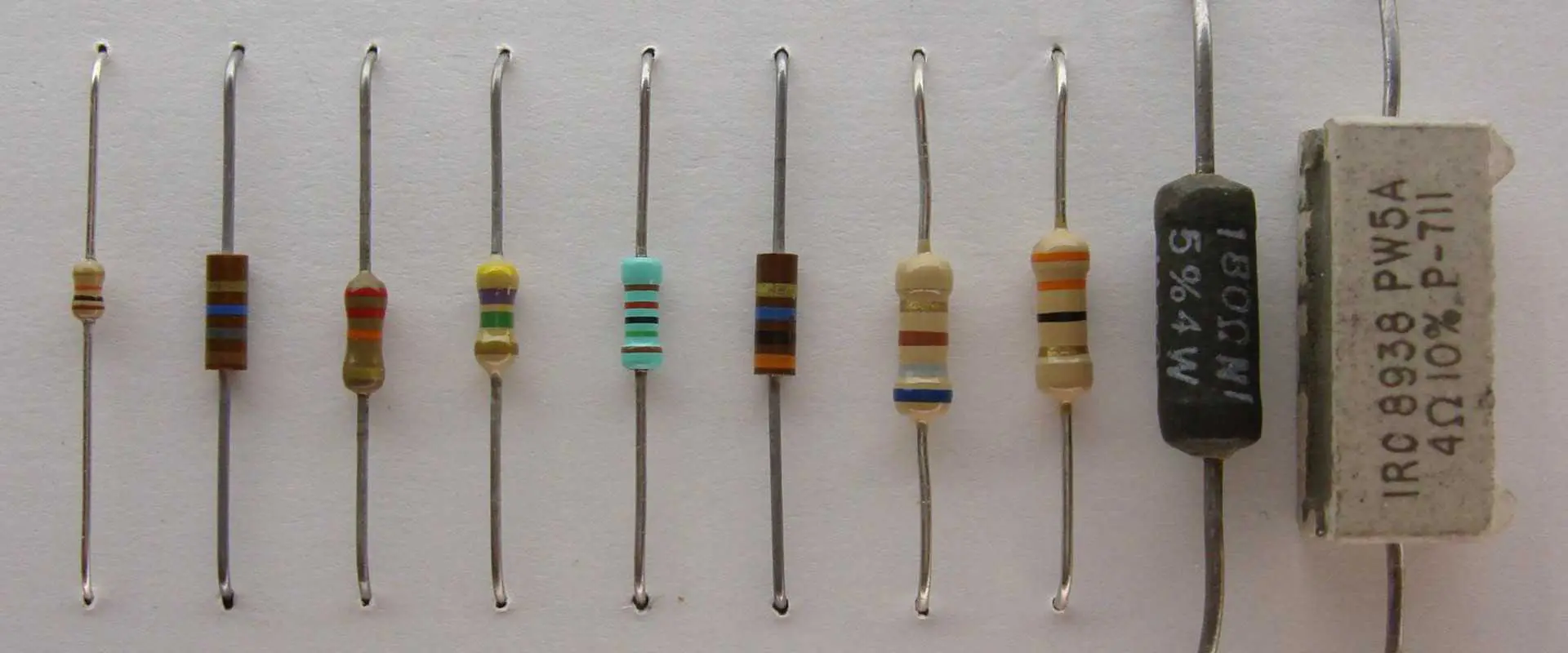
3. Board Materials

The choice of materials used for the production of PCB can affect its lifetime and operations. It can also have an impact on the thickness of the board. A simple board fabrication consists of the laminate, substrate, silkscreen, and solder mask.

The most important ones are the laminate and the substrate because they have a great impact on the overall thickness and structure of the board. Laminates consist of thermoset resin and either cloth layers or paper. On the other hand, the substrate consists of epoxy resin and paper, ceramic or glass weave depending upon the required dielectric constant.ย 

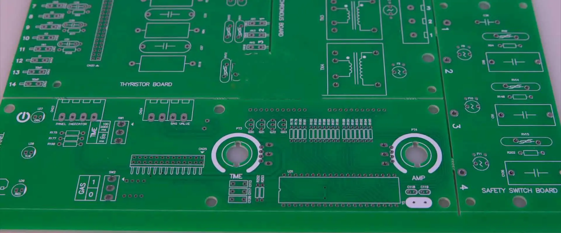
4. The Number of PCB Layers

FULL PCB MANUFACTURING Quote

Undoubtedly, the thickness of the board is influenced by the number of layers of PCB. The standard threshold of PCBs thickness falls between 2-6 layers but not more than eight layers. Manufacturers may use thinner layers of PCB to meet the standard thickness, but it is totally impractical as the layers increase in number.

If the design needs extra layers, then allow the increase in thickness of the PCB. If your design doesnโ€™t need those multiple layers and requires to meet certain parameters of thickness, then reduce the number of layers. 

5. Signal Types

There is a vast range of signal types that PCBs carry, which helps in identifying the materials that are required for the board and can also affect the thickness of the board. For example, if there is a board carrying high-power signals, it will require wider traces and thicker copper, which significantly makes it thicker than the boards that are operating with low-power signals. However, high-density boards having complex signals use thin traces, lasers, and thin high-performance materials, which makes them thinner than other types of boards.

Conclusion

Concluding this article on a note that using the right size, base material, number of layers, types of signals, and thickness tolerances for the plated and non-plated features plays a crucial role in determining the impact on PCB thickness. There’s always a need for PCB tolerances to make sure that the products are being properly used and processed. 

A guide to the Use of PCB Assembly Cost Calculator in Electronics

through-hole assembly process

Finding out how much a PCB assembly will cost is among the most difficult and time-consuming jobs for beginners. In addition to being a substantial contribution to an electrical gadget, PCB assemblies have advanced to the point where they need to be assembled by skilled hands.

In light of this, manufacturers absolutely cannot neglect the PCB assembly cost as another important factor. In addition to allowing manufacturers to estimate their overall costs, this cost also persuades them to constantly have all available tools at their disposal in order to minimize costs as far as possible. Even so, the overall cost or expenditure of PCB assembly would aid manufacturers in determining the optimal pricing for the finished product.

There are various factors that determine the overall cost of PCB. This article gives you a detailed insight into those factors.

PCB Assembly Cost Calculator | RayPCB Engineering Tools

PCB Assembly Cost Calculator

RayPCB Engineering Tools
Basic Info
Components
Services
BOM Upload
Board Specifications
mm
ร—
mm
Assembly Type
Lead Time
SMT Components
Through-Hole Components

Turnkey: We procure components based on your BOM. Consigned: You ship components to us.

Special Packages
Testing & Inspection
Additional Services
Quality Standards
Upload Bill of Materials
Click to upload or drag and drop
CSV, XLS, XLSX (Max 10MB)

Required BOM columns: Designator, Quantity, Manufacturer Part Number, Description, Package/Footprint

Gerber Files
Upload Gerber/PCB Files
ZIP, RAR (Max 50MB)
Additional Notes

Cost Estimate

10
Boards
235
Components
100
cmยฒ
Quote Completeness 65%
SMT Assembly $85.00
THT Assembly $25.00
Component Cost $120.00
Testing & Services $35.00
Stencil & Setup $50.00
ESTIMATED TOTAL
$360.00
Unit Price: $36.00/board
Estimated Lead Time 7-10 days

Cost Saving Tips

  • Increase quantity for better unit price
  • Use standard packages when possible
  • Consolidate unique part numbers
  • Choose economy lead time
  • Panel multiple designs together

PCB Assembly Cost Calculator for Transferring Data 

small-batch-pcb-assembly

Do you worry about how much PCB assembly will cost? Do you want to be informed of any unanticipated costs? You must first locate a reputable PCB assembly company if you want to learn everything there is to know about this pricing procedure.

Don’t let the abundance of choices you have overwhelmed you. Instead, the list makes your selection extremely difficult because it would be challenging to determine which company is a reputable one and why you should hire them. The general guideline is to contact a few short-listed PCB specialists and seek a price for printed circuit board manufacture based on the information supplied, taking into account the SMT technique utilized and the availability of money.

Make sure you make a list of all things that need to be analyzed by the selected manufacturer. Some of those are

  1. Centroid Data
  2. Assembly files
  3. Amount of layers of circuits
  4. BOM
  5. Gerber Files
  6. Uniqueness

PCB Assembly Cost Calculator

The PCB cost calculator starts working the moment the manufacturer begins information analysis. The professionals will enter the necessary data and wait for the calculator to provide a response. The amount so acquired is dependent on a number of important factors that may need to be changed if the actual cost turns out to be higher than anticipated.

To make modifications simple, once the calculator offers a number, it is essential to understand the price before assembly, particularly the cost of the material.

ยท Material Cost Before Assembly

The manufacturing business begins by obtaining bids for the electronic components and PCB bare boards, along with estimates for designing and PCB assembly charges to be added to the purchase amount. Because of capacitance disk loading, Surface-Mounted Technique chip, and resistance, the resulting must replace around 5% of the destroyed material. But the prices are offered with modifying SMT line, stencil, and processing file for lesser PCBA quantities.

ยท Solder Joint Cost

As every solder junction on a circuit board is unique and requires a separate processing procedure, SMT and DIP after welding are other important factors to take into account when estimating the cost of PCB assembly. A single solder pad is typically considered as one point, whereas the length of an IC solder junction is measured in feet. After 1206 SMD accuracy, with the exception of CD54 inductance, which is recorded to 12 points rather than the other solder pads’ 24 points, each solder pad is given two points.

The price ranges between 0.03 CNY and 0.008 CNY depending on the kind and other variables after accounting for every solder joint. The test time of the PCBA board, which covers packing logistics, the price of three proofing paint, and special packaging materials, is the next assessing factor. Moreover, the term FOB which is related to transactions, is also required to be added to the cost calculator of PCB assembly.

PCB Assembly Cost Calculator to Determine The Order Quantity

FULL PCB MANUFACTURING Quote

Order volume has a major impact on a commodity’s price, which is among the main fundamental principles of economics. A bigger order quantity typically results in lower product pricing.

The assembly of printed circuit boards is also subject to this guideline. For instance, paying $3.025 per unit for ten pieces of a standard 50mm ร— 50mm 2 layers order will cost you $30.25. You will pay $30.15 if you alter your order to 30 units at a price of $1.005 per item. You’ll save a ton of money on manufacturing as a result. For businesses searching for affordable SMT, it’s the ideal solution. As a result, a pick-and-place robot will be able to put the electronic components on the Assembly of PCB with ease.

PCB Assembly Cost Calculator for Single-Sided Or Double-Sided

The total cost of a PCB assembly is significantly influenced by the number of panels in the assembly. Every time there is a layer count rise, the price of a PCB typically goes up. In simple words, the price of the PCB increases each time a layer is added to the circuit board.

A double-sided PCB of 50 by 50 mm from several manufacturers costs about $16. It requires online information on purchasing customized PCBs.  

Conclusion

Engineers base their estimate of the cost of PCB assembly on a variety of factors. This occurs because the cost of producing electrical equipment is a very important consideration. The good thing is that you may make effective preparations for a PCB assembly job by making an accurate guess as to how much it will cost. All you have to do is carefully analyze a number of important variables that have an impact on PCB assembly costs.

Your company’s profitability can increase if you can reduce the cost of PCB assembly. Working with the proper PCB manufacturer is a clever method to keep prices low.

Choose the Top-Notch Quality Flight Controller PCB

drone PCB

Manufacturing a drone from scratch all by you is quite rewarding to work. However, choosing a flight controller can be challenging when you don’t even know the materials. Apart from other components that are used to create a flight controller for the drone, PCBs are an essential part.

Without a PCB, a flight controller of the drone is useless as it wouldnโ€™t operate as it needs to. A drone flight controller without the best PCB in it only reduces the overall functionality of the drone. 

This article gives you a detailed insight into why PCB is important in the flight controllers of a drone and what factors you should consider when looking for the right printed circuit for the flight controller of the drone.

1. Production Budget of Flight Controller PCB

Drone flight regulators or controllers are not cheap as one can imagine easily. If you do a little market research, then you might know that the flight controller of drones is quite expensive. But the price of the flight controllers is very high when selecting the best one. However, when you look for a flight controller of a drone in the market, see whether the materials used in it are cheaper and affordable or not, especially the PCB. 

If you have a specific budget, then make sure that the flight controller you choose for the drone must fit into that budget. You, yourself, don’t want to overstep your budget. To ensure the affordability of drones, it is essential to know whether the PCB used in them is affordable or not. And the PCB is actually the heart of the drone flight controller.

Choose flight controllers of drones that contain an affordable PCB. Well, it is also a notable thing that PCB does not come cheaper. They also come in expensive sizes, forms, and shapes. But affordability matters a lot in choosing the right flight controller for the drone, especially PCBs that need to function the drone properly.ย 

2. Trends of Flight Controller PCB

Popularity matters a lot to many people. If we look around, everyone is trying hard to be popular. This is the same scenario that goes for choosing the flight controller for the drone. However, this is not as easy. The best flight controller of a drone depends upon the popularity of the material used in it, especially the quality and material used in PCB. 

People literally see popularity as a good thing. They like to associate popularity with bigger things. Therefore, when choosing the right flight controller for the drone, it is an ideal choice to work with the popular PCB. Popular PCBs mean that the flight controller you choose works perfectly well as you desire.

Popularity also depicts the quality of products. If the product has the best quality, then this increases its certainty and makes it popular among people. However, it is essential to look at whether the flight controller of the drone is made with popular products or not. Choose people who have more interest. 

3. Specific Frame Size Of Flight Controller PCB

The flight controllers of the drone must have adequate size. This literally depicts that the PCB that powers the flight controller should have an ideal size. It’s quite hard and challenging to operate a drone that is too big in size.

The flight controller of a drone consists of various components. A PCB is among those several components. However, when you choose a flight controller, make sure that the PCB is ideal. Do not choose a flight controller that consists of a large PCB. Having a large PCB in the flight controller of a drone literally means it would be hard to operate the controller.

Again, make sure that the PCB used in the flight controller shouldn’t too small. Tiny or mini-size PCB means that it might reduce the overall functionality of the flight controller. Other than being small, there are a few things that might not operate well with a small PCB

Therefore, do not go for either too large or too small PCB in the flight controller of the drone. Choose the one with an adequate size that will not affect the functionality and performance of the drone flight controller.

4. Easy to Maintain Flight Controller PCB

When choosing a flight controller, reparability is one of the important factors that matter the most as you donโ€™t want to have a flight controller for the drone that would be hard to repair when damaged. In more simple words, do not select a flight controller whose PCB is hard to repair.

As you know, PCB is the heart of electronic devices. Same flight controllers also depend upon the PCBs used on them. Without it, or in case of damage, the flight controller can not function adequately. Therefore, make sure that the PCB must be repairable before choosing the drone flight controller.

The flight controller of drones is more at risk of damage. All the components used in it are prone to damage, but PCB is one of them. Therefore, while choosing the right flight controller, ensure that the PCB can be repaired easily. Moreover, one important thing to note is that not all PCBs can be fixed. That is why it is crucial to choose a flight controller whose PCB is safe and can be repaired in case of damage.

5. Materials for Flight Controller PCB

FULL PCB MANUFACTURING Quote

It is essential to look at which type of material is used in the PCB of the flight controller you choose, as PCB is the core of the drone flight regulators. When you are on your research tour to find the best flight regulator, make sure of the quality and usage of materials used in the PCB.

If you donโ€™t pay attention to the material of the PCB in the flight controller, it will end up in the non-functionality of the drone controller. Therefore, to be safe, ensure the high quality of PCB material while selecting the flight controller of the drone. The high quality and adequate choice of material ensure the functionality of the PCB, which ensures the high performance of the drone controller properly. 

6. Experience of Manufacturers 

Experience also matters a lot in the manufacturing of components used in the drone controller. Make sure that the PCB used in the drone controller comes from an experienced manufacturer. An experienced manufacturer ensures the quality and functionality of the product and reduces the risk of damage.

It is important to know that the PCBs used in drone flight regulators all come from well-experienced and skilled manufacturers. Experienced and skilled manufacturers have been working in the field of PCB for years, and they know the market trends well. Therefore, it is important to choose a flight controller with a PCB that comes from an experienced supplier. 

Experienced manufacturers see the market values, trends, and usage; there, they go beyond their limits to provide unified and consistent customer service with quality products.

7. Weight of Flight Controller PCB

Flying a bulky drone can be quite frustrating and hard. The weight of the drone matters the most as the PCB is one of the essential components of the drone controller, among other electronic components. 

Therefore ensure that the PCB used in the drone controller must have an ideal weight. As the weight of the PCB directly affects the weight of the overall drone controller. And you might not like to fly a drone that is too bulky and hard to carry. 

PCBs come in a variety of sizes, shapes, and forms. Some PCBs come with lightweight, while some come with heavyweight. However, if you want an inconvenience-free drone flight without concern about the weight, then make sure the PCB must be lightweight. This ensures that it is easy to carry anywhere. 

Conclusion

There are several versions of flight controllers for drones available in the market. Unfortunately, they are not all the best options. Some are not the best in proper functioning. The biggest reason for that is the PCB in them.

Without an adequate PCB in the flight controller of the drone, it wouldnโ€™t work. If you are looking for the best flight controller for your drone and donโ€™t know which factors to look for. Then ensure that the quality, material, size, and weight of the PCB are ideal. If it goes well, you will automatically find an ideal flight controller for your drone. 

FR4 Thickness Guide: Standard PCB, Core, Prepreg & Copper Thickness Explained

Isola FR406N PCB

Understanding the intricacies of FR4 thickness is crucial for designers, engineers, and manufacturers alike. This comprehensive guide delves into the various aspects of FR4 thickness, exploring standard PCB thicknesses, core and prepreg materials, and copper thickness. By the end of this article, you’ll have a solid grasp of these concepts and their importance in PCB design and manufacturing.

What is FR4 and Why is Thickness Important?

Understanding FR4 Material

FR4, short for Flame Retardant 4, is a composite material widely used in the production of PCBs. It consists of woven fiberglass cloth impregnated with an epoxy resin binder. The “4” in FR4 indicates that it meets the UL94V-0 standard for flame retardancy, making it an excellent choice for various electronic applications.

The Significance of FR4 Thickness

FR4 thickness plays a crucial role in determining the overall performance, durability, and functionality of a PCB. It affects several key aspects:

  1. Electrical properties
  2. Mechanical strength
  3. Thermal management
  4. Signal integrity
  5. Impedance control

Understanding and selecting the appropriate FR4 thickness is essential for ensuring optimal PCB performance across different applications.

Standard PCB Thicknesses

fr4-3mm-PCB

Common FR4 PCB Thicknesses

PCBs come in a variety of standard thicknesses to suit different applications. The most common FR4 PCB thicknesses include:

  1. 0.4 mm (15.7 mils)
  2. 0.8 mm (31.5 mils)
  3. 1.0 mm (39.4 mils)
  4. 1.2 mm (47.2 mils)
  5. 1.6 mm (63 mils)
  6. 2.0 mm (78.7 mils)
  7. 2.4 mm (94.5 mils)

Factors Influencing PCB Thickness Selection

When choosing the appropriate PCB thickness, several factors come into play:

  1. Application requirements
  2. Component height and weight
  3. Mechanical stress tolerance
  4. Thermal considerations
  5. Cost constraints
  6. Manufacturing capabilities

It’s essential to balance these factors to select the optimal FR4 thickness for your specific PCB design.

Read more about:

Core Thickness in FR4 PCBs

What is PCB Core?

The core is the central layer of an FR4 PCB, providing structural stability and insulation between conductive layers. It consists of a solid piece of FR4 material with copper foil bonded to both sides.

Standard Core Thicknesses

Common core thicknesses in FR4 PCBs include:

  1. 0.2 mm (7.9 mils)
  2. 0.25 mm (9.8 mils)
  3. 0.3 mm (11.8 mils)
  4. 0.4 mm (15.7 mils)
  5. 0.5 mm (19.7 mils)
  6. 0.6 mm (23.6 mils)
  7. 0.8 mm (31.5 mils)

Impact of Core Thickness on PCB Performance

The thickness of the core affects several aspects of PCB performance:

  1. Mechanical strength and rigidity
  2. Electrical insulation properties
  3. Thermal management capabilities
  4. Overall PCB thickness and stackup design

Selecting the appropriate core thickness is crucial for achieving the desired balance between these factors in your PCB design.

Prepreg Thickness in FR4 PCBs

Understanding Prepreg Material

Prepreg, short for pre-impregnated, is a type of FR4 material used to bond multiple layers of a PCB together. It consists of partially cured epoxy resin and fiberglass cloth, which becomes fully cured during the PCB manufacturing process.

Common Prepreg Thicknesses

Standard prepreg thicknesses in FR4 PCBs include:

  1. 0.064 mm (2.5 mils)
  2. 0.076 mm (3.0 mils)
  3. 0.1 mm (3.9 mils)
  4. 0.15 mm (5.9 mils)
  5. 0.2 mm (7.9 mils)

Role of Prepreg in PCB Stackup Design

Prepreg layers serve several important functions in PCB design:

  1. Bonding multiple layers together
  2. Providing insulation between conductive layers
  3. Controlling overall PCB thickness
  4. Influencing impedance characteristics
  5. Enhancing mechanical strength

Careful selection and arrangement of prepreg layers are essential for achieving the desired PCB stackup and performance characteristics.

Copper Thickness in FR4 PCBs

Understanding Copper Weight and Thickness

Copper thickness in PCBs is often expressed in terms of weight, measured in ounces per square foot. Common copper weights and their corresponding thicknesses include:

  1. 0.5 oz (17.5 ฮผm)
  2. 1 oz (35 ฮผm)
  3. 2 oz (70 ฮผm)
  4. 3 oz (105 ฮผm)
  5. 4 oz (140 ฮผm)

Importance of Copper Thickness

The thickness of copper layers in an FR4 PCB affects several critical aspects:

  1. Current-carrying capacity
  2. Heat dissipation
  3. Signal integrity
  4. Impedance control
  5. Manufacturing complexity and cost

Selecting the appropriate copper thickness is crucial for achieving the desired electrical performance and reliability in your PCB design.

Calculating Total FR4 PCB Thickness

Components of PCB Thickness

The total thickness of an FR4 PCB is determined by the combination of:

  1. Core thickness
  2. Prepreg thickness
  3. Copper thickness
  4. Number of layers

Step-by-Step Calculation Process

To calculate the total thickness of an FR4 PCB:

  1. Determine the number and thickness of core layers
  2. Add the thickness of all prepreg layers
  3. Include the thickness of copper layers on both external and internal layers
  4. Sum up all components to get the total PCB thickness

Understanding this calculation process is essential for accurate PCB stackup design and ensuring compatibility with mechanical constraints.

FR4 Thickness Considerations for Different PCB Types

Fr4 Laminate
Fr4 Laminate

Single-Layer PCBs

Single-layer PCBs typically use thinner FR4 substrates, ranging from 0.4 mm to 1.6 mm. Key considerations include:

  1. Mechanical strength requirements
  2. Component height and weight
  3. Cost-effectiveness for simple designs

Double-Sided PCBs

Double-sided PCBs often use FR4 thicknesses between 0.8 mm and 1.6 mm. Important factors to consider are:

  1. Plated through-hole requirements
  2. Balancing copper thickness on both sides
  3. Impedance control for high-speed designs

Multilayer PCBs

Multilayer PCBs can have varying total thicknesses depending on the number of layers and design requirements. Considerations include:

  1. Core and prepreg layer arrangement
  2. Impedance matching between layers
  3. Overall PCB thickness constraints
  4. Thermal management in high-density designs

Impact of FR4 Thickness on PCB Manufacturing

Manufacturing Processes Affected by FR4 Thickness

FR4 thickness influences several aspects of PCB manufacturing:

  1. Drilling and via formation
  2. Etching and plating processes
  3. Lamination and pressing
  4. Cutting and routing

Challenges with Extreme Thicknesses

Working with very thin or very thick FR4 PCBs presents unique challenges:

  1. Thin PCBs (< 0.4 mm):
    • Increased risk of warping and damage during handling
    • Difficulties in maintaining consistent thickness
    • Challenges in drilling small vias
  2. Thick PCBs (> 2.4 mm):
    • Increased drilling time and tool wear
    • Difficulties in achieving uniform plating in high aspect ratio vias
    • Challenges in maintaining consistent impedance control

Understanding these challenges is crucial for designing PCBs that are both manufacturable and cost-effective.

FR4 Thickness and Signal Integrity

How FR4 Thickness Affects Signal Integrity

The thickness of FR4 material in a PCB influences signal integrity in several ways:

  1. Dielectric constant variations
  2. Signal propagation delays
  3. Crosstalk between adjacent traces
  4. Impedance control

Optimizing FR4 Thickness for High-Speed Designs

For high-speed PCB designs, consider the following strategies:

  1. Use thinner dielectric layers to reduce signal propagation delays
  2. Implement controlled impedance traces
  3. Utilize proper stackup design to minimize crosstalk
  4. Consider alternative materials for critical high-speed sections

Balancing FR4 thickness with other design parameters is essential for achieving optimal signal integrity in high-speed PCBs.

FR4 Thickness and Thermal Management

Relationship Between FR4 Thickness and Heat Dissipation

FR4 thickness plays a role in PCB thermal management:

  1. Thicker FR4 layers provide better insulation but can impede heat dissipation
  2. Thinner FR4 layers may allow for better heat transfer but offer less electrical insulation

Strategies for Thermal Management in FR4 PCBs

To optimize thermal performance in FR4 PCBs:

  1. Use thicker copper layers for improved heat spreading
  2. Implement thermal vias to enhance heat transfer between layers
  3. Consider embedded heat sinks or metal core PCBs for high-power applications
  4. Optimize component placement and PCB layout for efficient heat dissipation

Balancing FR4 thickness with thermal management strategies is crucial for ensuring reliable PCB performance in high-power applications.

Conclusion

Understanding FR4 thickness and its impact on PCB design and performance is essential for creating high-quality, reliable electronic products. By considering factors such as standard PCB thicknesses, core and prepreg materials, copper thickness, and their interplay with signal integrity and thermal management, designers can make informed decisions to optimize their PCB designs.

As technology continues to advance, the demands on PCB performance will only increase. Staying informed about FR4 thickness considerations and best practices will help you navigate the complexities of modern PCB design and manufacturing, ensuring that your products meet the highest standards of quality and reliability.

The Differences Between Hot Swappable PCB and Solder PCB

hot swappable PCB

A PCB (Printed Circuit Board) that supports hot swapping enables quick removal and replacement of electronic components without shutting down or turning off the machine. As a result, users can quickly replace broken or obsolete parts without affecting the system’s functionality. Hot-swappable PCBs are frequently ideal in fields that need high availability and uptime, like data centers, servers, and industrial control systems. They offer a practical and effective method for maintenance and upgrades without generating downtime, increasing productivity, and lowering costs.

Hot swap Vs. solder PCB

Modern electronics come from printed circuit boards (PCBs), the framework for mounting and connecting electrical components. PCBs come in various forms, with hot-swap and soldered PCBs being two of the most popular. We shall examine the ten primary distinctions between hot-swappable and soldered PCB.

Replacement of Components:

The main distinction between hot-swap and soldered PCBs is the ease with which electrical components can be removed and replaced with hot-swap PCBs without the requirement for desoldering. On the other hand, with soldered PCBs, the components must first be desoldered to be removed and replaced.

Flexibility:

Comparatively speaking, soldered PCBs are less flexible than hot-swappable PCBs. Soldered PCBs need the system to be powered down and cooled before replacing components. However, hot-swap PCBs allow users to change or upgrade components immediately without disrupting the system’s operation.

Cost:

Because they are more flexible and complicated, hot-swap PCBs are typically more expensive than soldered PCBs. In addition, connectors and the hot-swap mechanism require extra parts, which might raise the PCB’s overall cost.

Power Consumption:

hot swappable keyboard

Hot-swap PCBs can consume more energy than soldered PCBs since they need more power to run the connectors and hot-swap mechanism.

Complexity:

Hot-swap PCBs are more complicated than soldered PCBs because they need extra parts for connectors and the hot-swap mechanism. As a result, Hot-swap PCBs may be more challenging to design and produce due to their complexity.

Size:

Due to the additional components needed for the connectors and hot-swap mechanism, hot-swap PCBs are often bigger than soldered PCBs.

Maintenance:

Compared to PCBs that are soldered, hot-swap PCBs require less maintenance. Users can quickly swap out components with hot-swap PCBs without affecting the system’s functionality, reducing maintenance downtime. Contrarily, desoldering components from soldered Boards necessitates additional maintenance and can be time-consuming.

Durability:

Due to the extra parts needed for the connectors and hot-swap mechanism, soldered PCBs are often more durable than hot-swap PCBs. Moreover, soldered PCBs provide a more reliable connection between the components and the PCB, which can lessen the risk of damage and increase the system’s overall toughness.

Customization:

Due to the additional parts needed for the hot-swap mechanism and connectors, hot-swap PCBs can be customized more than soldered PCBs. More customization possibilities may be possible with this added flexibility, which may benefit particular systems or applications.

Application:

Hot-swap PCBs are frequently helpful in sectors including data centers, servers, and industrial control systems that demand high availability and uptime. In addition, electronics that are more geared at consumers, such as laptops and cell phones, frequently use soldered PCBs.

How do I know if my PCB is hot-swappable?

FULL PCB MANUFACTURING Quote

There are a few things to check to know if a PCB is hot-swappable. Indicators that a PCB is hot-swappable include the following:

Connectors:

On the PCB, look for connectors that are necessary for hot-swapping. These connectors can simplify component removal and replacementโ€”desoldering is not usually necessary.

Labels:

Certain PCBs may contain a label indicating they are hot-swappable or a symbol indicating it is on the PCB. Check for signs that the PCB is ideal for hot-swapping, such as labels or symbols.

User Guide:

See the user guide or product specifications to determine whether the PCB is intended for hot-swapping. Instructions on swapping components without shutting down the system might be in the manual.

System Design:

The PCB is likewise ideal for hot-swapping if the system is hot-swappable. Again, verify whether the system is essential for hot-swapping by consulting the system documentation or contacting the manufacturer.

Industry Standard:

The PCB is more likely to be hot-swappable for usage in sectors that need high availability and uptime, such as data centers, servers, and industrial control systems. Verify if the PCB complies with industry standards, such as the ATCA (Advanced Telecom Computing Architecture) or PICMG (PCI Industrial Computer Manufacturers Group), frequently supporting hot-swapping.

Examples of hot-swappable devices

hot swappable pcb

Devices that can be swapped or removed from a system without shutting it down or interfering with service are known as hot-swappable. These devices are crucial for high-availability systems and applications where downtime is not an option. Hot-swappable gadget examples include the following:

Hard Drives:

Servers and storage systems frequently use hot-swappable hard drives. We can change these drives instantly, making upgrades and maintenance simple without affecting the system’s functionality.

Power Sources

Hot-swappable power supplies are utilized in data centers and other crucial equipment to ensure high availability and redundancy. Both power supplies can seamlessly take over if one fails.

Cooling Fans:

Servers and other high-performance systems employ hot-swappable cooling fans to regulate the temperature and avoid overheating. Without turning the system off, we can change these fans changed immediately.

Network Interface Cards (NICs):

Hot-swappable NICs are necessary for servers and network appliances to offer redundancy and guarantee ongoing network connectivity. If a NIC malfunctions, we can change it without affecting service.

Memory Modules:

Servers and other systems employ hot-swappable memory modules to simplify upgrades and maintenance. In addition, these modules are interchangeable on-the-fly, making it simple to scale the memory capacity.

Input/Output (I/O) Modules:

Network switches and routers use hot-swappable I/O modules to simplify upgrades and maintenance. The network traffic can continue to run while these modules are changed.

Controllers for RAID:

Storage systems use hot-swappable RAID controllers to add redundancy and guarantee high availability. In addition, we can switch these controllers out instantly without affecting how the system works.

Fan systems:

Servers and other high-performance systems employ hot-swappable system fans to regulate the temperature and avoid overheating. Without turning the system off, we can change these fans changed immediately.

Power Distribution Units (PDUs):

Data centers and critical systems employ hot-swappable PDUs to ensure high availability and redundancy. If one PDU malfunctions, the other can take over immediately.

Blade Servers:

Data centers and other high-performance systems use hot-swappable blade servers to simplify upgrades and maintenance. In addition, we can easily replace these servers without affecting the system’s functionality.

Summary

In conclusion, hot swappable PCBs provide more flexibility, but at a cost and with more energy use. They also take up more room and are more complicated, but they are easier to maintain and have more customizing choices. PCBs with solders are less flexible and have fewer customization choices, but they are more cost-effective, robust, and power-efficient. The application and system requirements will determine whether hot-swap or soldered PCBs are best.

Hot-swappable devices are crucial for high-availability systems and applications where downtime is not an option. These tools simplify upgrading and maintaining systems without affecting how they work, assuring continued availability and dependability. Numerous hot-swappable device types are available to satisfy the requirements of various systems and applications, ranging from hard drives to blade servers.

You should speak with the manufacturer or a licensed engineer if you are still unsure whether your PCB can be hot-swapped. They can offer additional instruction and support to help identify whether the PCB is hot-swappable and how to properly change components without harming the system.

Smart Gas Meters, are they worth your Money?

Smart Gas Meters

Smart gas meters are the modern standard meter versions efficiently designed to accurately measure gas. Moreover, these tools let you monitor meter readings which you can then submit to your gas supplier. Using these tools, you can be able to achieve accurate reading without having to consult experts.

Typically, smart gas meters have DCCs or private national communication networks. These networks help users submit their gas tracking information to their suppliers without going to the supplier’s physical location. Moreover, the new advanced smart gas meters also have home displays. These displays let you track and read gas consumption data plus how much the consumption rate will cost you.

These smart gas meters are truly revolutionary and are termed the next big thing in the gas industry. However, for a device to gain this much hype, it has to entail more than what meets the eye. Therefore, what exactly does a smart gas meter do? What features does this component entail? And should you invest in a smart gas meter?

What are Smart Gas Meters?

smart gas meter board

Typically, smart gas meters are intelligent gadgets that help users determine the amount of gas that they have utilized within a given timeframe. Moreover, what makes these gadgets distinct when compared with conventional versions is the fact that they can directly and wirelessly send the reading from your gas to your gas supplier within seconds. Doing so helps save you money and time you could have spent traveling to the supplier’s locations to show them your readings and make payments.

Moreover, users don’t have to hire experts to read and track their gas meters after installing smear gas meters. Instead, they can perform these actions in the comfort of their home.

How do Smart Gas Meters Operate?

Smart gas meters, unlike smart gas meters, check how much gas you have utilized over a span of 30 minutes. They then submit this reading to the gas supplier via smart electricity meters. Smart electricity meters, on the other hand, have to be installed in a center. After installation, these gadgets automatically monitor your power consumption and generate a report.

Like when you are utilizing a PC in a network, you should connect the smart gas meters to a network to transmit their reading to the gas supplier. To cater to this need, you should connect to an intelligent, secure network known as a DCC. This network is called DCC because it is usually operated by a Data Communication Company that ensures the integrity of the data shared in the network. Moreover, the DCC handles the submission of your gas reading.

Moreover, intelligent gas meters also come bearing in-home displays that you can utilize to monitor your gas consumption. Using this display, you can quickly establish how much gas you have consumed.

Benefits of Smart Gas Meters

FULL PCB MANUFACTURING Quote

Intelligent gas meters are, without a doubt, more efficient when compared to traditional gas meters. However, if you are still doubting this, then here are some pros to convince you:

Hassle-Free

Smart gas meters come bearing a display that you can easily integrate into your house. Using this display, you can effectively monitor your gas consumption rate with little to no hassle. Moreover, using this same display, you can quickly determine whether you have been utilizing more gas than usual and then apply the necessary measure to bring this consumption rate down. Altering your gas usage according to the reading that you get from this display can help you save a lot of cash.

Complete Control

One of the main reasons why intelligent gas meters were created is to help gas users monitor and alter their gas consumption habits to impact them positively. Moreover, people who utilize smart gas meters can efficiently process their gas readings via computer software programs and then generate an overview of their gas consumption rate.

Due to this, consumers and utility providers can effectively share gas consumption info to help them make the right decisions.

Accurate Gas Consumption Readings

A smart gas meter will send accurate readings of your gas consumption rate to your utility provider on a monthly, daily, or hourly basis, according to your configuration. Due to their level of accuracy, these gadgets eliminate the issue of bill estimation, which primarily affects the consumer negatively. Therefore, by installing these gadgets, you get to pay for the exact amount of gas that you utilize, not more and not less.

With traditional meters, which were not intelligent, if you failed to submit your gas reading, the gas supplier would have to estimate the amount of gas you spent using past bills. However, these estimations are almost always inaccurate. However, using a smart gas meter, you can avoid this issue and ensure that you don’t get shocked by large gas bills at the end of the month.

Easy Understanding

Smart gas meters display information in a format that is user-friendly. Moreover, the units are well converted to ensure that the user doesn’t struggle when reading. All these help eliminate the need for experts to carry out gas consumption readings.

Cheaper Tariffs

Smart gas meters have not been in the market for long. Therefore most people don’t know about them and their benefits. To curb this issue, gas suppliers are providing cheaper tariffs and exclusive discounts for businesses and homes with smart gas meters. Therefore, if you search for the right supplier, you can get cheaper tariffs, which will help you save more money.

Easier to Change Suppliers

By utilizing intelligent gas meters, you will not have to take final readings when you want to change your supplier. Therefore, if you’re going to shift from one gas supplier to another, you will not have a hard time compared to when you are utilizing a traditional gas meter.

Disadvantages of Smart Gas Meters

Millimeter wave PCB

Smart gas meters, without a doubt, have multiple benefits, especially concerning monitoring gas consumption. However, installing these gadgets doesn’t mean you will gain lower gas bills automatically. There are several issues that users should know before they purchase intelligent gas meters, these include:

Utilization of Mobile Signal

First Gen smart gas meters utilize signals from mobile networks to send information. And while smart gas meters don’t use traditional internet connections or Wi-Fi, if you reside in remote areas with patchy mobile signals, this will also significantly impact your gas’s smart meter.

However, the DDC (Data Communications Company) is setting up a dedicated wireless smart meter net which will be able to solve this issue once and for all. According to statistics from the data communications company, the communication coverage of smart gas meters is available to more than 99% of the United Kingdomโ€™s households.

Smart Gas Meters do not Guarantee that Users will Save Money

Smart gas meters do not help you save money in an autonomous manner. On the contrary, smart gas meters will only allow users to save cash if they take the monitoring of gas consumption seriously. Using the display that comes with the smart gas monitor, user can easily monitor their gas consumption and then alter their behavior to reduce the amount of gas they use. However, if users don’t do this, then they will save little to no cash in terms of gas bills.

Excessive Monitoring

The display that comes with smart gas meters is advantageous, without a doubt. However, it also comes with one downside. The downside comes in when users check on their gas consumption via the display every now and then in an obsessive manner. Doing so could quite easily lead to friction among family members. It is impossible for users to cut out gas consumption entirely, and trying hard to achieve lower bills could lead to family members getting angry whenever someone uses the gas, even in the proper manner.

Smart Gas Meter Printed Circuit Boards

Printed circuit boards or PCBs are traditional names used to refer to bare boards which manufacturers utilize to effectively mount various electrical components that are integrated to form an electrical device. Moreover, PCBs are utilized to electrically connect and mechanically support various electronic components using conductive paths or tracks, which are etched from laminated sheets of copper.

When the circuit board only bears copper features and tracks and doesn’t have any circuit elements, for example, active devices, resistors, or capacitors, you should call it a PWB or a Printed Wiring Board.

Today, printed circuit boards are utilized in virtually every electronic product you come across, from simple, mass-produced products, to more complex devices. Moreover, these components help manufacturers gain full automation throughout their production process, which boosts their profits and efficiency.

Relation of PCBs with Smart Gas Meters

Smart gas meters utilize high-quality printed circuit boards to achieve their level of efficiency in terms of information computations and transmission. Actually, most, if not all, smart gas meters have a printed circuit board bearing the following specifications:

  • Minimum size โ€“ 0201
  • Min BGA pitch โ€“ 0.3 millimeters
  • Printed circuit board size โ€“ 130 by 128
  • Welding spot โ€“ 1124

Moreover, in the assembly of these printed circuit boards, manufacturers mostly face the following challenges:

  • Applying ENIG surface finishes
  • Gold Finger
  • Assembly of various components under intense heat

Conclusion

Smart gas meters have become increasingly popular due to their ability to effectively send gas readings to various gas suppliers automatically and wirelessly. Therefore, using this gadget, you do not have to travel long distances to deliver your gas reading to your gas provider. And even though these components have some downsides, they do not outweigh their advantages. Therefore, if you are looking to purchase a smart gas meter, we recommend that you try it out.

How to Solder Electronics

electronic assembly soldering

Mastering soldering techniques to solder electronics is one of the essential skills that every manufacturer must learn. This article gives you a detailed insight into the soldering types, soldering irons, soldering stations, desoldering methods, and some safer measures to follow.

What Is Soldering in Electronics?

If you ever look closely at an electronic device with a printed circuit board, there you see that all the components of the circuit board are integrated through soldering methods. Soldering is a method of integrating the components and another electronic part on the surface of the circuit board by placing a melting solder mask around the components. A solder is generally a metal base that gives a strong and firm electronic connection between the components when it cools down.

Soldering Electronics Tools

SMT-Through-Hole-Soldering

One of the best things about learning soldering skills is that it is not complex and doesn’t require much from you. There are various soldering tools that help in the soldering process. Some of the most used soldering tools are described below.

ยท Soldering Iron:

Soldering Iron is a manual tool operated by plugging into the power supply of 120V AC. When the current passes through the iron, it heats up and melts the solder. A soldering iron is one of the important and widely used soldering tools. It is available in distinct forms, like a gun or pen, depending upon its usage. For starters, pen form soldering iron is mostly recommended between the range of 15W to 30W. Moreover, some soldering comes with variant tips that can be interchangeable and used for different purposes. A standard soldering iron can warm up to 896 Fahrenheit; therefore, use it carefully while using it. 

ยท Soldering Station:

The soldering station is considered the latest version of the traditional soldering pen. It is a great choice if there are a lot of components to solder. Moreover, its flexible features and controlling features make it an ideal choice. One of the biggest benefits of using a soldering station is that it allows for adjustment of the heat of the iron according to device requirements. Moreover, these soldering stations come with temperature sensors, password settings, and alert settings and give a quite safe space for work.  

ยท Soldering Iron Tips:

The end part of the soldering pen or iron is known as the soldering Tip. Most of the soldering irons come with an interchangeable soldering tip. These tips come in a variety of sizes and shapes depending on their usage. Each Tip is specially designed to offer specific benefits and purposes. The Chisel tip and the Conical Tip are both commonly used tips in almost all electronic projects.

  1. Chisel Tip consists of a broad flat pin which is ideal for soldering larger components or wires. 
  2. Conical Tip consists of a fin tip which is especially used for attaining precision in the soldering process since it has a very pointed tip that ensures the transfer of heat even to smaller spaces without causing any disruption in the surroundings. 

ยท Brass or Conventional Sponge:

Conventional or brass sponge is also one of the most important soldering tools. It helps in cleaning the iron tip of the soldering iron. It ensures the removal of the leftover oxides on the iron tip. Due to oxidation on the iron tip, it gets black and does not accept more solder than it did before. A wet sponge can also be used though it might affect the lifespan of the iron due to contraction and expansion. Moreover, it also drops out the temperature of the soldering iron tip when it is used. Therefore, brass sponges are always a good option. 

ยท Soldering Iron Stand:

A soldering Iron stand is one of the basic tools, and it also gives a handful of benefits. It keeps the hot soldering iron away from the other flammable materials that might get caught fire accidentally when it comes into contact with it. This could also lead to hand injuries. Most of the soldering irons come with a built-in stand and cleaning brass sponge. 

ยท Solder

FULL PCB MANUFACTURING Quote

The soldier is a mixture of metals that is used to bond electrical components together by melting them. There are both lead-free and lead variations of solder. They also come with different diameters like 0.062โ€ and 0.32โ€. Under the core of the solder, there is a flux named material that supports improving mechanical strength and electrical connection between the components. 

Rosin lead-free core solder is one of the common types of soldering for electronic devices. This solder is basically a mixture of Copper or Tin. It also comes with lead, of which 60% is tin and 40% is lead. But this soldier is losing their fame as it affects health. However, always wash your hands, and do proper ventilation before using lead solder.

Always choose a non-acid core solder because the acid core might damage the components and circuits. Solder with the acid core is commonly sold at house maintenance stores and is widely used for metalworking and plumbing.

Since solder comes in various forms and diameters, the diameter of 0.062โ€ of solder is ideal for soldering bigger joints faster. However, it might not work well with smaller joints. Therefore, make sure to have both soldiers with distinct diameters. 

ยท Helping Hand

The Helping hand is a type of device with two or sometimes more alligator clips. It also contains a magnifying lens in some variations. It helps you in holding the components that you need for soldering while you manage the soldering iron. This is one of the most helpful tools that you should have in your working space.

ยท Soldering Safety

As you already know, what types of soldering tools and devices are used in the soldering process of electronic devices? Here are some practical safety tips that ensure your safety during soldering.

The soldering iron has a temperature limit of over 800โ€™ Fahrenheit which is quite a lot of high. Therefore, it is recommended to use an iron stand that protects from unwanted events of fire and burning.

Always ensure to work in an open space or ventilated space. During the heating process of solder, the alloy releases toxic fumes, which can be dangerous for the lungs and eyes. That is why it is recommended to install a fume extractor. It is a type of fan that contains a charcoal filter that ensures that no harmful toxins are left in the room.

Moreover, always use glasses while working with solder as the hot solder might get a splash on your eyes. 

Last but most importantly, always wash your hands after the soldering process so that there wonโ€™t be a toxin left on your hands.

ยท Tinning The Tip

Before starting the soldering process, the first step is tinning the Tip of the soldering iron with the solder. This supports the transfer of heat faster from the soldering iron to the soldering components. Tinning also ensures the reduction of wear and protects the iron tip. 

  1. First, ensure that the Tip is firmly attached and screwed well in place.
  2. Turn on the power of the soldering iron. Leave it for a few minutes to heat up. If you are using a soldering station, then you can adjust the temperature to 400โ€™C 
  3. Take a cleaning sponge and clean the Tip of the iron with a wet sponge. Left the iron on the stand to warm up again.
  4. Then hold the solder in one hand and the soldering iron in another. Touch the iron tip with the solder and ensure that the solder flows swiftly around the iron tip.

You can also repeat this process after the soldering session too. It enhances the life span of soldering.

How To Solder Electronics? 

1. Mount The Components:

First of all, start with the wires of LEDs. Put them in the drill holes of the printed circuit board. Flip the circuit board and bend the wires on the outer side at an angle of 45โ€™. This helps in creating a better connection of the components with the copper board and protecting it from dropping during the soldering.

2. Heat The Joint:

Turn on the power of the soldering iron and let it heat up. If it has adjustable temperature control, then set the temperature to 400โ€™C. Then touch the iron tip to the resistor lead and the copper pad simultaneously. Put the soldering iron at the exact point for almost 3 to 4 seconds to heat the lead and pad up.

3. Apply Solder To Joint:

Keep holding the soldering iron in the same position as touching copper and lead, and then touch the solder with the joint. An important thing to note here is that you never touch the iron tip directly with the solder. You have to be sure that the joint is heated enough to melt the solder right away. If the joint is cold, then it will create bad connections.

4. Snip The Leads:

Remove the iron from the joint and let it cool down the solder naturally. Donโ€™t blow over the solder to cool it down, as it makes bad connections. Once the solder is cool down, snip the exaggerated wires from the leads. 

A perfect joint is shiny and smooth and gives a cone and volcano shape look. Just put enough solder so that the joint will be covered. Too much solder makes a solder ball which can be spilled over other joints or leads.

Desoldering

One of the good facts about soldering is that it can easily be removed through a process called desoldering. This helps in removing the component as well as making corrections in the soldering process. For the desoldering process, you just need a solder wick, also referred to as a desoldering braid.

  1. Place a small piece of solder wick or desoldering braid over the solder tip you want to remove.

Heat up the soldering iron. Touch the iron tip to braid. This heats up the solder, which will be absorbed by the braid. Remove the desoldering braid and check whether the solder was removed properly or not. Touch the braid carefully, as it still might be hot.

Powering the Industries with IoT Factory and Manufacturing

Smart Manufacturing IoT

Industry 4.0 surely possesses various incredible benefits to offer and developed immensely in the past few years. However, Industry 4.0 still needs to go a long way to overcome some hurdles. For instance, cybersecurity is one of the major concerns which was brought forward by the 4th Industrial revolution era.

This article gives a detailed insight into the benefits and disadvantages of Industry 4.0 and tells factors to keep in mind while making digitization initiatives in the factory.

ยท IoT Factory for Improved Productivity & Less Machine Downtime

Industry 4.0 helps in producing mass production by keeping track of resources and using them in a very efficient and cost-effective manner. It simply means that technologies of Industry 4.0 help you produce more with fewer resources.

Production lines and machines also face less downtime due to integrated sensors, AIs, and IoT devices which keep track of integration, enhance the monitoring system and automate the decision-making process. OEE means the overall effectiveness of the equipment also improves as all the systems are connected with each other due to Industry 4.0 and make a smart factory.

ยท IoT Factory for Improved Efficiency

Due to the integrated technology of Industry 4.0, production lines have also become efficient. Some already mentioned efficiencies include less downtime of machines and greater production with fewer resources.

Other significant efficiencies brought by Industry 4.0 technologies include the automatic process of tracing and tracking quick batch changeover and automatic reporting. This also improves the efficiency of NPIs and their decision-making ability.

ยท Optimised Supply Chain Management 

The technologies, systems, and processes of Industry 4.0 give complete and better visibility of the supply chain. The supply chain also gets connected and goes through real-time monitoring and management with improved collaboration and communication.

For instance, it helps in analyzing the bottlenecks and other problems related to the supply chain faster before impacting the overall production line. This advanced knowledge of problems helps in taking better correction steps.

The supply chain also becomes agile and more resilient, enhancing abilities to respond faster and accurately to the demands of customers and market values.

ยท Optimized Product & Factory Life Cycles With Digital Twins

The technology of digital twins collects them from the real world, makes a digital copy of the data, and updates the systems immediately. This twin digital data can be the twin of finished products, production lines, or data of the entire factory.

This technology of digital twin allows for analysis of efficiency and performance and gives a shot to different scenarios to see how it works without affecting the real output. This also helps in improving innovation.

ยท Empowered People:

With the technology of Industry 4.0, workers could get a hand with better and improved data, which helps them to get insight into things well and enables them to make better decisions.

Moreover, it also reduces the need for workers to work on the same tasks. Automated and advanced technology workflow handles the repetitive tasks and gives you a space to use the human resources at some other valuable place.

ยท Increased Knowledge Sharing 

Silos are the sole operating systems in traditional manufacturing factories. Silos basically facilitate individuals and the individual machines they use. This could lead to less knowledge sharing or collaboration.

Industry 4.0 integrated technologies allow business processes, production lines, and floors to collaborate and communicate without concern about time, location, platform, zone, and other factors. For instance, the data gained from one sensor integrated into a machine will be shared throughout the factory.

Moreover, it doesn’t need human intervention to operate; all the data can be saved automatically from one system to any other system. In simple words, data gathered through one sensor is automatically transferred to all other systems around the factory and production lines all over the world. 

ยท Flexibility & Agility:

Industry 4.0 also enhances agility and flexibility. For instance, this makes it easy to mount production either up or down in smart factories. Moreover, it also allows introducing the new product in production while creating opportunities for high mix and on-off manufacturing.ย 

4 Levels Of IoT Factory 

FULL PCB MANUFACTURING Quote

There are four stages that help in accessing the journey of improvement to becoming a smart industry.

1. Basic Data Availability:

This is the beginning step where the factory is in the traditional state. There is a set of collected data in the system, but it is not analyzed and accessible. The analysis of data can take quite a long time, which can affect the efficiency of the production process.

2. Proactive Data Analysis:

This level ensures access and analysis of data in an organized form. The data is available and is organized through display assisting and visualization in the process. This allows analysis of proactive data, yet there are still improvements needed.

3. Active Data:

This level enables the analyzing process of data through artificial intelligence and machine learning without getting any help or supervision from humans. At this stage, the system is more automated than level two and helps in predicting the anomalies and key issues of potential failures.

4. Action-Oriented Data:

The fourth stage follows level three to work on the solution to the problems detected in level three. In most cases finding solutions and implementing them mostly don’t need human intervention. In simple words, at this stage, all the data is gathered and analyzed well, problems are predicted, and solutions are also generated, which can be implemented with little or no human input when needed.ย 

Technologies Used In A IoT Factory 

The smart factory contains a variety of distinct and advanced technologies brought up by Industry 4.0 to optimize and improve the manufacturing process. Some of these advanced technologies are described below/

ยท Sensors:

Sensors are integrated into machines and devices to collect data for monitoring at certain stages of the process of manufacturing. For instance, sensors can sense variables in temperature and other such factors and have the ability to correct them or warn the staff right away. These sensors are linked to a connected monitoring system which provides a network among all machines.

ยท Cloud Computing:

After collecting data from sensors, cloud computing is used to process and store those data. It is a much more efficient, cheaper, and flexible way that allows users to upload, access, and store an excess amount of data and also to give feedback for making decisions in real time. 

ยท Big Data Analytics:

The data collected also helps to use this data to get an insight into the performance of the production line. However, Big data allows us to spot error patterns in the data and provides an assurance of quality with an immense degree of precision. This data allows you to share it with factories and enterprises to fight and solve common issues together and optimize the process.

ยท Virtual & Augmented Reality:

Augmented reality is a type of digital technology consisting of digital information collected through reality and can be accessed through smart devices. Virtual reality is more like a virtual world that needs special types of spectacles to see that world. Both these superb technologies help smart factories to optimize the production process, organize the products, and repair and maintenance of machines.

ยท Digital Twins:

A digital twin is used to mimic or create a digital replica of real-world objects and update its performance in reality. This not only improves efficiency but also helps in operating and controlling the planning.

Why BlackBerry IoT is the most preferred platform for hacking

BlackBerry IoT

BlackBerry IoT (Internet of Things) is a platform that gives businesses access to and control over IoT devices in a secure manner. With capabilities like device administration, data analytics, and real-time connectivity, the platform provides end-to-end security and scalability for IoT installations.

The company’s decades of expertise in mobile security and enterprise applications form the foundation of the BlackBerry IoT platform. In addition, it addresses the particular security issues that IoT devices face because they frequently have constrained computational power and are open to assaults.

The platform offers capabilities like remote device administration, over-the-air updates, and secure data exchange to create an adaptable and safe environment for managing IoT devices. Additionally, it contains comprehensive analytics and visualization tools for processing and analyzing IoT data. As a result, it allows businesses to obtain knowledge and make wise decisions.

Automotive, healthcare, and industrial automation are just a few industries that employ BlackBerry IoT. In addition, organizations can build and manage IoT solutions with ease and confidence thanks to the platform’s ability to operate with various IoT devices, sensors, and gateways.

What are the three main components of IoT?

A network of linked devices that gather and exchange data online is known as the Internet of Things (IoT). IoT devices are widely essential in various sectors, including healthcare, transportation, and agriculture. Additionally, they are critical to developing more effective and efficient systems. IoT consists of three integral parts:

Devices:

The physical items that gather and send data are devices in an IoT system. These gadgets may include sensors, cameras, and other observational tools that collect information about the surroundings and the present things. Additionally, IoT gadgets can range in complexity from a basic temperature sensor to a sophisticated autonomous car. Wi-Fi, Bluetooth, cellular, and satellite are just a few communication protocols that can link these devices to the internet.

Networks:

The infrastructure of an IoT system that links the devices to the internet and one another is the networks. IoT networks might be private or public, wired or wireless. Wi-Fi, Bluetooth, Zigbee, and cellular networks are the most widely used wireless IoT networks. Edge computing devices are small gadgets that can process data and carry out other operations at the network’s edge, near the devices, in IoT networks. For lowering latency and preserving bandwidth, edge computing is essential.

Cloud services:

The third element of IoT is cloud services. It offers a means of processing, storing, and analyzing the data produced by IoT devices. Cloud services such as storage, analytics, and machine learning are available to make sense of the data. Additionally, it provides insights that we can use. Therefore, we can examine the data immediately or later for analysis. The management tools that enable enterprises to manage and monitor their IoT devices remotely are also part of cloud services.

These three elements combine to form an IoT system that can gather, analyze, and take immediate action on data. For instance, a smart home system might have sensors that track temperature, motion, and light levels and transmit that information to a central hub over a wireless network. Furthermore, the hub can use cloud services to program smart lighting, thermostats, and other devices. Additionally, a smartphone app can operate and monitor the system remotely.

Why BlackBerry IoT

FULL PCB MANUFACTURING Quote

Because BlackBerry IoT offers a target-rich environment with great potential for monetary gain or disruption, hackers use it. Unfortunately, BlackBerry IoT is not immune to the threat of hacking as IoT devices spread across various businesses. The following are some causes for which hackers might target BlackBerry IoT:

Financial Gain:

Financial gain is one of the main reasons why hackers attack BlackBerry IoT. So, the IoT platform is a tempting target for attackers attempting to steal and monetize this data since it may contain valuable data. Examples include customer information, payment details, or sensitive business data. Additionally, hackers may exploit this data to commit identity theft, launch ransomware attacks, or make money by selling it on the dark web.

Exploiting Vulnerabilities:

The BlackBerry IoT platform might have flaws that hackers could exploit to get unauthorized access, just like any program or system. As a result, hackers can use these flaws to infect the platform with malware or ransomware or to access confidential data.

Botnets:

A hacker or group of hackers can operate networks of infected devices known as botnets. IoT devices frequently have fewer security protections than conventional computing equipment. As a result, this makes them particularly susceptible to botnet assaults. To build a botnet from which to launch distributed denial of service (DDoS) assaults or other forms of cyberattacks, hackers can employ BlackBerry IoT devices.

Weak Passwords:

Many IoT devices’ default or weak passwords, including those running the BlackBerry IoT platform, are frequently guessable or hackable. As a result, hackers can use these vulnerable credentials to obtain unauthorized access to the platform.

Supply Chain Attacks:

In a supply chain assault, hackers may potentially target BlackBerry IoT devices. In this scenario, an attacker breaches the network of a manufacturer or supplier to obtain a product before making it available to end customers. Additionally, hackers can access the BlackBerry IoT platform and linked devices by compromising it during the development or distribution phases and installing malware or backdoors.

Espionage:

In rare instances, hackers might use BlackBerry IoT devices as a target for espionage. This can entail stealing intellectual property or secret business information from a targeted company.

How to protect

BlackBerry IoT device

Use security best practices to defend BlackBerry IoT and the connected devices it connects against these threats. Here are a few pieces of advice:

Keep Devices and Software Up to Date: Ensure that the most recent software and firmware are available on every device connected to the BlackBerry IoT platform. As a result, it makes it easier to make sure that vulnerabilities are patched and secured.

Use Strong Passwords: For all devices and accounts on the BlackBerry IoT platform, use secure and distinctive passwords. Additionally, one should not share passwords between users and should change them frequently.

Implement Two-Factor Authentication: Two-factor authentication offers an additional layer of protection by requiring a second form of identity in addition to a password, such as a text message or mobile app.

Use Encryption: In the BlackBerry IoT platform, we should encrypt every data transfer between devices to avoid interception or eavesdropping by unwanted parties.

Limit Access: Only give those who require access to the BlackBerry IoT platform. Make sure users only have access to the exact information and features they require to do their jobs by using role-based access controls.

Regularly Monitor and Audit the Platform: Watch the BlackBerry IoT platform frequently for unusual behavior or suspicious activity. This entails running vulnerability scans, auditing user activities, and reviewing logs.

Educate Users:ย Inform all BlackBerry IoT platform users about security best practices, such as using strong passwords and recognizing phishing emails.

Programming languages used for BlackBerry IoT

Using the BlackBerry IoT platform, we can securely manage Internet of Things (IoT) devices. Like most software platforms, we create BlackBerry IoT utilizing a range of programming languages to accommodate the many parts that make up the platform. Some of the programming languages employed in the creation of BlackBerry IoT are listed below:

Java:

The BlackBerry IoT platform was mostly a Java product. Java is a popular programming language for creating enterprise applications. However, the platform may run on various operating systems and devices thanks to the language’s cross-platform interoperability.

C/C++:

Low-level programming languages like C and C++ are frequently essential in embedded systems and IoT gadgets. In addition, these languages are renowned for their speed and memory management, which are necessary for IoT devices with limited resources.

Python:

Python is a high-level programming language used for data analysis and scripting. It is frequently combined with other programming languages to create sophisticated Internet of Things (IoT) applications.

JavaScript:

In creating IoT user interfaces, JavaScript, a popular programming language for web development, is frequently employed. Additionally, JavaScript is beneficial for creating responsive and interactive user interfaces for Internet of Things applications.

Go:

Go is a more recent programming language created by Google intended to create scalable and effective software applications. It is beneficial for creating distributed systems and microservices frequently utilized in IoT applications.

Rust:

Using Rust’s programming language, we can develop system-level applications with great performance and memory safety. In addition, building IoT devices that need low-level control and real-time processing makes use of it exceptionally well.

Swift:

Apple created the programming language Swift to create apps for iOS and macOS. The creation of BlackBerry IoT’s mobile apps. As a result, it lets users manage IoT devices from their smartphones, and make use of it.

SQL:

While maintaining and querying data kept in databases, Structured Query Language (SQL) is the best database language. Therefore, we can frequently store and retrieve data from IoT sensors and devices using SQL to create IoT solutions.

Bash:

Bash is a popular scripting language for Unix shells used in creating IoT solutions. As a result, its scripts can automate processes, including the deployment and configuration of IoT devices.

Lua:

In embedded systems and IoT devices, a lightweight scripting language called Lua is frequently ideal. Building compact and effective IoT solutions is where Lua shines.

Summary

Devices, networks, and cloud services make up IoT systems. Together, these elements build a network of physical devices capable of data collection and exchange. IoT has the power to change a variety of sectors and build better, more effective systems. Organizations may improve their operations and make better decisions by utilizing the data produced by IoT devices.

For several motives, including monetary gain, vulnerability exploration, the development of botnets, and espionage, hackers target BlackBerry IoT.

Different programming languages are helpful depending on the exact BlackBerry IoT component desired. The platform primarily uses Java but also other programming languages to support its numerous components, including C/C++, Python, JavaScript, Go, Rust, Swift, SQL, Bash, and Lua. By considering the performance, memory utilization, and other requirements of an IoT solution, developers can select the optimal programming language for their particular use case.

Everything You Need to Know About 3.3K Resistor

Resistor color

A 3.3K ohm resistor is a type of electronic component. It is helpfulย to limit the flow of electric current in a circuit. The term “kohm” is short for kilo-ohm, which means that the resistor has a resistance of 3.3 thousand ohms. This resistor has a variety of applications, such as voltage dividers, LED circuits, and other electronic circuits.

A 3.3K ohm resistor is an electronic component that has a resistance value of 3,300 ohms. It will limit the amount of current that can flow through it, according to Ohm’s Law.

What Is the Color Code of 3.3K Resistors?

The color code for a 3.3K ohm resistor is orange, orange, red, and Gold. Each color on the resistor corresponds to a specific digit or multiplier value, as follows: Orange has 3 digit values spectrally for both orange bands. The red band is the multiplier, while the Gold band is the tolerance band. Every color band shows different values in the resistor. These color bands make every resistor unique. You can notice that the color code is different for every resistor. If you buy two resistor forms, different vendors both have the same color code. It means that both have the same resistance. If their color code is different, then it means that both have different resistance. That’s why color codes are important for resistors. For example, the color code of the 2.2 k resistor is Red-Red-Red-Gold.

Advantages of 3.3K Resistor

6 Strip Resistor

A 3.3K ohm resistor has following advantages:

1. Wide Availability

3.3K ohm resistors are widely available in the market, making them easily accessible for various electronic applications. So you donโ€™t need to worry.

2. Compatibility And Precision

The 3.3K ohm resistor is compatible with many electronic circuits, and it can be used in various applications such as voltage dividers, current limiters, and signal conditioning circuits. These resistors are available with high precision, making them suitable for use in precise circuits where accurate resistance values are required.

3. Highly Stable

3.3K ohm resistors are very stable over time and temperature. This makes them ideal for use in circuits where stable and reliable performance is essential.

ยท Inexpensive

 3.3K ohm resistor is an inexpensive resistor. These resistors are relatively inexpensive compared to other electronic components, making them a cost-effective choice for electronic circuit design.

4. Low Power Dissipation

 3.3K ohm resistors have low power dissipation, which means they do not generate much heat when in use, making them suitable for use in circuits where heat dissipation is a concern. You know that heat dissipation is one of the problems in circuits.

What Is the Difference Between 3.3k Ohm Resistor And A 3.2 K Ohm Resistor?

FULL PCB MANUFACTURING Quote

The main difference between a 3.3K ohm (kilo-ohm) resistor and a 3.2 K ohm resistor is its resistance value. A resistor with a value of 3.3K ohm has a resistance of thirty-three hundred ohms, while a resistor with a value of 3.2 K ohm has a resistance of thirty-two hundred ohms. This means that the 3.3K ohm resistor will allow more current to flow through it compared to a 3.2 K ohm resistor when connected to the same voltage source, assuming all other factors are equal.

It’s also worth noting that the tolerance, or the amount by which the resistor’s actual resistance may deviate from its stated value, could be different for these two resistors. Typically, resistors have a tolerance of 5 percent or 10 percent, which means their actual resistance could vary by that amount from the stated value.

A 3.3K resistor is not inherently different from other resistors in terms of its basic function – that is, to resist the flow of electrical current. However, it may have specific characteristics or properties that make it suitable for certain applications.

The main difference between a 3.3K resistor and other resistors is simply its resistance value. The “k” in 3.3K stands for kilo-ohms, which means the resistor has a resistance of 3,300 ohms. Other resistors may have different resistance values, such as 1 ohm, 10 ohms, 1000 ohms, or even several mega-ohms. Specific resistance of resistor makes it suitable for different circuits. Their resistance decides their placement in circuit. Thatโ€™s why it important to know the resistance of resistor.

Some Frequently Asked Questions.

THT Resistor
THT Resistor

ยท From Where Can I Buy Top Quality 3.3K Resistors?

 There are several vendors on many online platforms. They are selling electronic components, including 3.3K resistors, in bulk. Read the reviews regarding your selected vendors and then go for purchase. If reviews and ratings are good, then you must go for them. If you find some negative reviews, then consider it a red flag. A reliable vendor will provide you best quality electronic components.

ยท Which Resistor Is Best Between 3.3K And 3.9 K Resistors?

The choice of which resistor to use in a circuit depends on the specific requirements of the circuit, such as the desired current flow and voltage drop.

If the circuit requires a higher resistance, then the 3.9 K resistors would be the better choice. On the other hand, if the circuit requires a lower resistance, then the 3.3K resist would be the better choice.

It is important to note power rating of the resistor also affects the choice of the resistor. Tolerance and the temperature coefficient are also important. Therefore, when selecting a resistor, it is important to consider all of these factors. As a result, you can choose the resistor that best meets your needs.

Conclusion

 3.3K resistor has its unique importance in the electronics world. It has multiple uses, so it is necessary to know how to use it in the circuit. Overall, the 3.3K ohm resistor is a versatile and reliable component. Its availability, compatibility, precision low cost, and low power dissipation make it an excellent choice for many applications. So whenever you are going to design circuit then must consider it.