There are two different types of electric circuits based on the components arrangement in the circuit. These are series circuit and parallel circuit. A series circuit is a type of circuit whose components are connected in a chain, while a parallel circuit has all the circuit components linked between two common points. Parallel and series circuits function as current divider circuits and voltage divider circuits, respectively. You can learn more about the current divider circuits here as that will be our main focus.
What is Electric Current?
Electric current refers to the movement of electrons in a conductor. It could also be defined as the movement of electric charge in an electric field. Electric current is usually measured in amperes (A). When the Amperes is greater, this indicates more flow of electricity. You can understand electricity better if you imagine it as the flow of water in the river.
Current and voltage are two different elements. While current is the movement of electrons, voltage is the amount of force used to push the electrons. An electric current will flow more when the voltage is higher and vice versa.
Resistance can affect the flow of current. Resistance is simply the width via which flow of electrons occurs. The width will be narrower when the resistance is greater. In contrast, a low resistance enhances the width via which the electrons will flow. Therefore, this enables the flow of more current at once.
What are Current Dividers?

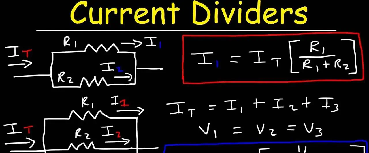
Current dividers refer to parallel circuit whose current supply divides into several parallel paths. The terminals of the components in a parallel circuit are linked together. These terminals share similar two end nodes. Therefore, there are different branches and paths for flow of current. However, these current can feature various values via each component.
The parallel circuits are current dividers since it can dive or share total current into several parts. A current divider is a linear circuit whose output current is a part of its input current. You can achieve this by connecting two or more current elements linked in parallel.
The current divider formula is applicable in situations where there is a parallel network of various elements. Also, the current divider rule formula can help you determine the current in every branch of a circuit. The main use of the current divider is to help generate a proportion of the available total current in the circuit.
But, the component integrated in transmitting the current has a restricted amount of current that flows via the component in some cases. Overcurrent can result in heat dissipation and also shorten the life span of the components. Therefore, a current divider allows the reduction of the flow of current via a component and as such, smaller component size can be integrated.
For instance, in a situation where you need a greater resistor wattage, heat dissipation can be decreased when multiple resistors in parallel are included.
Current Divider Rule Formula
Current divider rule formula helps in minimizing complexity while determining current in any circuit. The current divider divides the current in small parts. Current divider prevents circuits against overheating. As the divider divides the aggregate current in small parts, there is generation of small current components and prevention of high current flow. Therefore, this reduces heat dissipation and as well prevents circuits from any damage.
The formula for a current divider is Ix=IT {RT/RX}
Where,
IX = Current through any resistor in the parallel circuit = V/RX
IT = Aggregate current of the circuit = V}/RT
RT= Equivalent resistance of the parallel circuit
V = Voltage across the parallel circuit = IT RT = I X R X (this is because the voltage is similar across the parallel circuit’s components).
The current divider rule formula states that the current of every branch of a parallel circuit is a proportion of the aggregate current input to the circuit.
What is the Difference Between Current Divider Formula and Voltage Divider Formula?

Most times, people confuse these two formulae. One important way to remember each of these formulae is to always remember that the two rations in the current divider and voltage divider equations should always be less than one.
Since we understand that the total resistance in a voltage divider circuit is more than any of the individual resistances, the fraction for the formula must remain as Rn over RTotal.
In terms of application
Voltage divider differs from current dividers in terms of application. Voltage divider is applicable in high voltage measurement devices. You can easily measure high voltages when direct measurement can destroy device. In a situation like this, an ideal option is to make use of the voltage divider. This helps to minimize the voltage to a safe region. For voltages that are extremely high, a great option is integrate capacitive instead of resistive ones.
The current divider formula is applicable in situations where there is a parallel network of various elements. Also, the current divider rule formula can help you determine the current in every branch of a circuit. The main use of the current divider is to help generate a proportion of the available total current in the circuit.
But, the component integrated in transmitting the current has a restricted amount of current that flows via the component in some cases. Overcurrent can result in heat dissipation and also shorten the life span of the components. Therefore, a current divider allows the reduction of the flow of current via a component and as such, smaller component size can be integrated.
Another application of voltage divider is when you need to determine an unknown resistance. Can you determine some unknown resistance if there is a voltage source and there is another resistor having known resistance?
It will be great if you are able to read its color code. However, color code might not be available. The best thing is to design a simple circuit that has both resistors properly arranged in series and determine the voltage over the resistor. After this, you can just input all these values in the voltage divider calculator.
When Can You Use Current Divider Rule Formula?
The current divider rule formula is applicable in the following circumstances:
- It is ideal for use in cases whereby two or more circuit elements are linked in parallel with the source of the current or the source of the voltage.
- Also, the Current divider rule can help in determining separate branch currents when the value of the equivalent resistance and the aggregate circuit current are known.
- When there is a connection between two resistors in a parallel circuit. In such a case, the current in any branches will only be a proportion of the total current (IT)). Also, if the values of two resistors are equal, the current will equally divide via the two branches.
- The current divider rule formula is applicable in a case where there are connections among three or more resistors in parallel. Here, the equivalent resistance will divide the aggregate current into proportional currents for every branch in the parallel circuit.
Frequently Asked Questions
What is Voltage divider with current source?
A voltage divider with a current source is used in dividing the voltage supply in the resistances. Also, the voltage drop across a resistor can be determined by multiplying the resistances with the current in the circuitry.
What are the benefits of current divider?
- Current divider rule formula helps in minimizing complexity while determining current in any circuit. The current divider divides the current in small parts.
- Current divider prevents circuits against overheating. As the divider divides the aggregate current in small parts, there is generation of small current components and prevention of high current flow. Therefore, this reduces heat dissipation and as well prevents circuits from any damage.
What is a high current voltage divider?
A high current voltage divider can offer a high amount of current. It is difficult to develop this type of voltage divider with a traditional resistor network. You can make use of a buck converter or switching regulator in this case. You can replace the voltage reference of the buck converter approach with a divider generated from the incoming supply.
What is the limit of a voltage divider current?
There is no particular limit for voltage divider current. According to some observations, some values suggest that currents more than 1 amp are high for voltage dividers.
Conclusion
Current and voltage are two different elements. While current is the movement of electrons, voltage is the amount of force used to push the electrons. An electric current will flow more when the voltage is higher and vice versa. The current divider formula is applicable in situations where there is a parallel network of various elements. Also, the current divider rule formula can help you determine the current in every branch of a circuit. The main use of the current divider is to help generate a proportion of the available total current in the circuit.