Major Differences Between Attiny85 programming Vs. atmega328p programming

Attiny85 programming Vs. atmega328p programming

Atmel, a prominent producer of microcontrollers that use various electronic appliances, features two highly sought-after microcontrollers: the Attiny85 and Atmega328P, both hailing from an AVR family. Despite sharing certain similarities, these microcontrollers exhibit notable differences in terms of their programming, which we will delve into in this piece.

It’s widely accepted that Arduino development circuit boards are a go-to option for novices in electronics, and with good reason. These boards facilitate effortless connectivity with other components and can be easily programmed via a user-friendly IDE and a simple USB cable. Additionally, they are in open-source form and boast a vast, dynamic association that is ever ready to offer assistance.

The boards themselves are also crafted in a manner that emphasizes sound design. Provided one essential basic prudence, it’s unlikely that they will cause permanent damage to the Arduino board. As a starting point for those interested in circuit design or programming, the Arduino circuit platform is an excellent way to gain initial exposure to these areas.

YouTube video

As projects become more complex or when creating products for consumer sale, the limitations of the Arduino platform become more evident.

In this article, we delve into the Attiny84, ATtiny85, and ATtiny2313 AVR microcontrollers, which are commonly used to move beyond Arduino-based prototypes to refined or optimized projects. We also compare these chips to an ATmega328 found in an Arduino Uno.

Disadvantages of Using an Arduino Programming

Attiny85 programming

Compared to a microcontroller IC, Arduino circuit boards are pretty bulky, making it challenging to integrate and embed into projects. Typically, shields incorporate Arduinos into larger projects by plugging into headers on the top of an Arduino. However, this approach often results in bulky assemblies that may not fit seamlessly into other aspects of a project.

The second drawback of Arduino boards is their relatively high cost compared to building custom boards with the microcontroller IC or associated passive elements. Relying on a model, Arduino circuit boards range from $20 – $30, while the microcontrollers applied in those circuit boards cost around or under two dollars. Additionally, the specifications of Arduino boards may be excessive For the activities they are commonly used for. Upon examining a selection of typical Arduino projects, it becomes apparent that many of the Arduino’s I/O pins remain unused, or the Programs executing on board Do not measure up to filling a Microcontroller’s flash storage.

ATtiny85 Microcontroller & Its Working

It is a viable substitute for the ATmega328P in small projects where only a few I/O pins are required. It is because using the ATmega328P’s limited I/O pins for small projects may not be efficient. In contrast, ATtiny85 microcontrollers can be utilized for small projects that require all available I/O pins. This article overviews the ATtiny85 microcontroller, including its pin diagram, advantages, specifications, disadvantages, and applications.

ATtiny85 is a high-performance, compact AVR microcontroller that utilizes the RISC CPU. It comes in two packages commonly used for interfacing and controlling various sensors or devices. The microcontroller also boasts Low-power usage through its MSSP and 10-bit ADC. The instruction code for this microcontroller is stored in RAM – 512 bytes and EEROM – 8kb. Alternatives to the ATtiny85 microcontroller include the ATtiny45, ATtiny25, ATtiny25V, ATtiny45V, and ATtiny85V.

Functions of ATtiny85 Microcontroller

The ATtiny85 microcontroller can perform multiple functions within a single IC. Specific pins on the microcontroller are useful for more than one function. Some of the primary functions of the microcontroller comprise timers, BOD, I2C communication, SPI communication, Interrupt, and ADC. The ATtiny85 microcontroller also features various memory types, such as FLASH, EEPROM, and SRAM.

Runing ATtiny85 Microcontroller Carefully

FULL PCB MANUFACTURING Quote

Microcontrollers are delicate components that require careful handling to achieve optimal performance and longevity in any software.

It is crucial to ensure that the electrical supply for the controller does not exceed 5.5V. Before connecting the controller to the digital multimeter, it is essential to confirm the accuracy of a voltage source output using the accurate digital multimeter. It is crucial to note that the DC output for each input/output pin must not exceed 40mA, while the DC output for GND pins and positive supply should not exceed 200mA.

To ensure a proper power supply, it’s essential to confirm the polarity of the microcontroller pins beforehand. To locate the microcontroller, an integrated circuit socket can be utilized on a circuit or breadboard. By doing so, the microcontroller is protected from the heat generated during soldering.

The Storage temperature limits for this controller span from -65ยฐC-+150ยฐC, while the operating temperature range is between -55ยฐC to-+125ยฐC.

Advantages of ATtiny85 Microcontroller

Here are some benefits of using an ATtiny85 microcontroller:

  • The power consumption is lower.
  • Easily Available
  • Less cost
  • Its small and compact size allows for easy arrangement within the tiny boards.
  • This microcontroller provides readily accessible reference data for convenient usage
  • Capable of integration via Arduino IDE.
  • Various power-saving modes enable this controller to function in battery-powered applications.
  • Despite having fewer pins, this provides numerous features.
  • This microcontroller possesses much program memory to meet the requirements of various applications.

Applications of ATtiny85 Microcontroller

The following are among the functions of the ATtiny85 Microcontroller.

  • Various engineering projects can be designed utilizing this microcontroller, depending on specific requirements.
  • The following are examples of commercial and educational applications that can be utilized.
  • Applications related to security and automobiles.
  • Industrial machinery control systems.
  • Systems involving weather sensors.

Programming an AVR ATmega328P with an Arduino

The Arduino Uno microcontroller board is powered by the ATmega328P microcontroller, which enables easy pin interfacing. The Arduino microcontroller board includes a USB serial interface and a 16 MHz clock, features not found on a standalone microcontroller. Arduino boards are ideal for prototyping, as they facilitate rapid iterations of designs. However, for finalized projects, they can be excessive depending on the features employed. Official Arduino Uno boards cost $20, while standalone ATmega328P microcontrollers cost about $2. Therefore, after completing the prototype phase with an Arduino, the project can be migrated to using the independent ATmega328P.

One potential challenge is the inability to link the ATmega328P to a computer for program uploads directly. To address this issue, a separate programmer is required. Fortunately, if an Arduino is available, it can be utilized as the programmer for an ATmega328P. So this guide outlines how to code the standalone ATmega328P by leveraging an Arduino or the Arduino development environment, using pure C code except for the built-in functionalities provided by the Arduino development environment.

Preparing and Connecting the Arduino

atmega328p programming

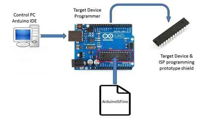
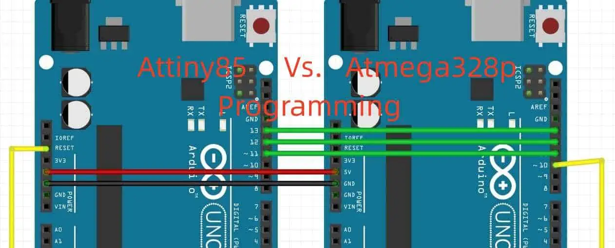
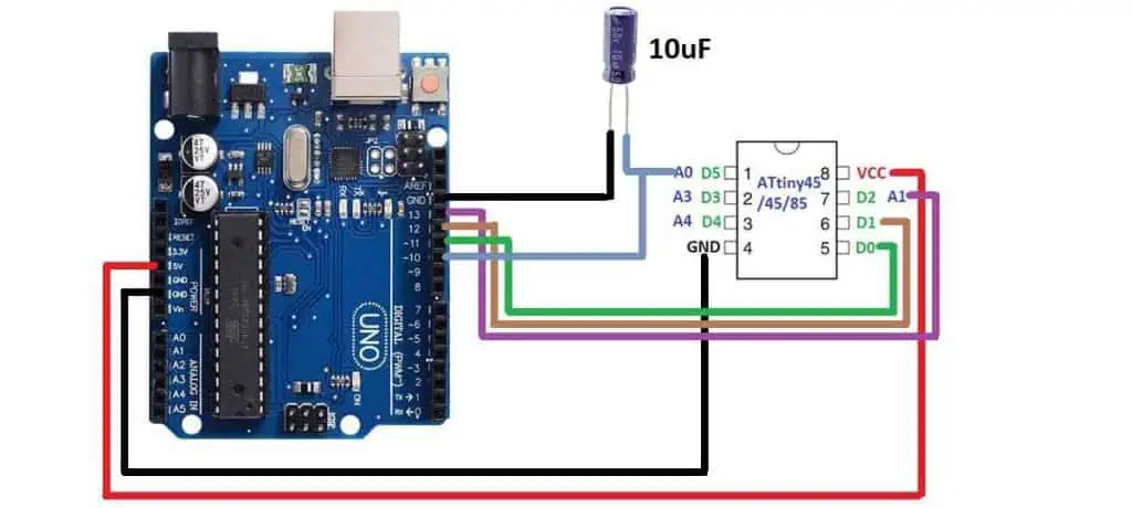
Before an Arduino Uno can function as an ISP, a specific sketch must be uploaded. Once uploaded, the Arduino Uno will be capable of programming the ATmega328P. To set up the Arduino Uno as an ISP, the following process must be taken:

To access the ArduinoISP software navigate to File -> Examples -> ArduinoISP -> “ArduinoISP.”

Upload an ArduinoISP sketch to the Arduino in the typical manner used for any additional sketch.

Having configured the Arduino as the ISP, it can now be utilized to code the ATmega328P. The SPI bus will link the Arduino to an ATmega328P by accurately linking the SPI connectors. However, this can be a complex task as the pin no. on an Arduino does not correspond directly with the pin no. on the ATmega328Peven, though the Arduino employs an ATmega328P chip itself. To ensure that the appropriate pins are connected, a comparison must be made between the PINs of the Arduino and those of ATmega328P. The image below displays the necessary pin connections for SPI, illustrating how these Arduino connectors correspond with those of the ATmega328P.

Differences Attiny85 programming Vs. atmega328p programming

1. Flash Memory:

The primary disparity between Atmega328P and Attiny85 is the quantity of flash storage accessible. Attiny85 possesses a mere 8 KB of flash memory, whereas Atmega328P contains 32 KB. Consequently, Attiny85 can accommodate a smaller number of commands than Atmega328P. Programmers must, therefore, produce more optimized code and maximize the limited memory capacity in Attiny85.

To surpass this constraint, programmers working with Attiny85 often employ optimization techniques like function performance optimization, data structure performance optimization, and loop unrolling. These methods assist in reducing the memory needed by the code, making it possible for Attiny85 to manage more complex applications.

Pins:

A significant distinction between Atmega328P and Attiny38 refers to their pin count. While Attiny85 has only 8 pins, Atmega328P has twenty-eight pins. It implies that Attiny85 has a limited number of input/output pins, which can restrict the number of elements linked to it.

Due to its limited number of pins, Attiny85 programmers must find innovative ways to connect components to the microcontroller. They may use multiplexers to enhance the I/O pins, shift to expand output pins, or analog signal multiplexers to share pins among multiple components.

2. Clock Speed:

The high speed of Attiny85 is 20 MHz, while Atmega328P is 16 MHz. Therefore, Attiny85 can execute instructions at a higher speed than Atmega328P. Although, the advantage of the higher clock speed is negated by the fact that Attiny85 has less flash memory available than Atmega328P.

Attiny85 programmers should be cautious in choosing the clock rate since it can affect the energy usage of microcontrollers. A faster clock rate may result in greater electrical consumption, which could be problematic for battery-operated applications.

3. Peripheral Support:

It has peripherals compared to Attiny85, including USART, API, and I2C interfaces, providing more comprehensive support for communication protocols and devices without requiring additional components. It is not the case for Attiny85, which has limited built-in peripherals, making it less versatile in device support.

Attiny85 microcontroller has smaller integrated peripherals than Atmega328P, including USART, SPI, and I2C interfaces. This makes it challenging for Attiny85 to support various devices and communication protocols without additional components. Therefore, Attiny85 operation may have to use external Serial Peripheral Interface (SPI) interfaces or software-based Inter-Integrated Circuit (I2C) protocols to interact with other equipment.

4. Programming Language:

Atmega328p with arduino bootloader

C is the programming language supported by both Attiny85 /Atmega328P, but there are differences in how a code is optimized and compiled for every microcontroller. Programmers using Attiny85 require a specialized compiler, like the AVR-GCC compiler. It is useful for AVR architecture.

It must know how to make its programs use less memory and run faster to work appropriately on the microcontroller. They also need to know what parts of a microcontroller they can use and how they can use them to make the program work well.

5. Programming Environment:

Attiny85 and Atmega328P use different programming environments. The Arduino integrated development environment is commonly useful by Attiny85 programmers as it provides an easy-to-use interface for compiling, writing, or updating code to a microcontroller. The Arduino integrated development environment (IDE)also has pre-built examples and libraries.

Conclusion

To summarize, Attiny85 or Atmega328P have commonly used microcontrollers with different functions. Attiny85 has less memory, less number of pins, or a faster clock speed. Therefore, Attiny85 programmers must optimize their code, use creative methods for connecting components, and consider power consumption when Choosing the clock speed.

Atmega328P has more built-in functions than Attiny85, which makes it better suited for appliances that need to work with more types of devices or communication methods. Both microcontrollers are programable using the same language, but the Attiny85 programmers require a specific compiler and know how to use optimization techniques effectively.

In summary, the decision to use Attiny85 or Atmega328P depends on the specific needs of the tool. If additional memory capacity and support for more peripherals are essential, Atmega328P can be better. However, if a smaller size is essential, Attiny85 can be a good option. Both microcontrollers provide developers with excellent capabilities or flexibility for various applications.

How to laser QR Code on PCB Board

Laser QR Code PCB

Advanced and latest marking technology includes laser coding devices. The text and patterns are etched on the product’s surface using focused laser etching technology. Laser marking, which is frequently employed in the Circuit sector, offers a number of advantages over the conventional inkjet printing approach. This includes good quality, great wear resistance, high consistency, efficiency, safety, cost savings, and dependability.

Smartphones, wearable gadgets, and such items are getting lighter and more compact. This is all because of the rapid expansion of the IT industry and increasing customer demand for more electronic goods. Refining production is also necessary. The inscription of symbols, one or two-dimensional bar code, and various data on the surface of the PCB are tracked back to achieve the highest quality assurance of the manufacturing process of the PCB. This has now become the industry’s development trend.

Due to weak wear resistance, lack of accuracy, environmental impact, and poor aesthetics, the conventional printing method is becoming more unable to meet the demands of the market for new technologies. Therefore, the PCB sector has started to use laser marking machines more frequently.

Engraving on the PCB’s surface can take the shape of a pattern drawing, corporate LOGO printing, QR code, contacts information, etc. Silk-screen printing was frequently used in the past for traditional printing. Conventional inkjet printing methods could have satisfied the market’s initial demands, yet since electronic products’ quality keeps rising, consumer expectations are also rising. This has led to an increase in the market’s demand for PCB boards with increasingly high labeling quality.ย 

Old-fashioned printing techniques cannot adjust to changing market demands, and their flaws are more evident, including:

  1. There has weak wear resistance. The level of wear resistance indicated here does not refer to the metal’s wear resistance. This indicates that the type of ink that covers the PCB’s surface is frequently worn away, resulting in discoloration and blurring.
  2. Requirements for aesthetics; because surface printing of metal has a comparatively low-end look. It is unsuitable for some items with stringent aesthetic standards, like medals, metallic business cards, elegant corporate nameplates, descriptions of handicrafts, etc. Meet their standards for looks.
  3. It is crucial to utilize chemical solvents, like heavy metal components and organic solvents. These solvents contain a specific level of toxicity and can harm the silk screen process of printing employees. Additionally, some volatile chemical components progressively volatilize as the ink of screen printing dries, polluting the atmosphere and harming the environment. A number of issues with conventional printing technology have been effectively resolved by the development of fiber-laser engraving technology. High accuracy, quick speed, and consistent performance define it. 

Additionally, it just requires computer control, is easy to use, and can produce a variety of intricate characters, patterns, two-dimensional bar codes, and such. This fully satisfies the demands of high-quality markings of the current PCB industry.

Attaching PCB QR Code With the Assembly

QR CODE PCB
QR CODE PCB

The complexity of a QR code increases with the number of characters in the URL it redirects to. In actuality, the size of the QR code is determinable by the length and the level of error correction. However, we advise users to build a short URL that points to the authentic and original address to solve this problem. The ideal and perfect URL must not contain over twenty characters.

Generating The PCB QR Code 

Numerous websites and software allow for the creation of QR codes. The producer of the QR code must utilize the same origin going forward to renew the code to guarantee the same picture for all items. However, not each tool employs a similar encoding process. Although some online software and tools include more possibilities, the following are the most important factors to take into account when creating.

  • Error correction makes it possible to identify mistakes and recreate the original and mistake-free data. M is recommended since it permits the recovery of 15% of code words.
  • Color: The majority of QR reader software is set up to scan dark or black QR codes over a white backdrop. Prior to being used on silkscreen, the QR bar code must be reversed if the backdrop is dark (for example, the color of the solder mask contains red, black, green, or blue). The QR needs not to be reversed if the color of the soldering mask is white.
  • Size: After import, the finished QR code must measure >0.5 in. Certain tools for converting images to DXF support resampling. If it does not, the right size of the pixel can be selected while the image is being generated.
  • Margin around QR code: Although Freescale has effectively utilized a 10% margin around QR codes, 20% is the appropriate margin.
  • UTF-8 recommends encoding.

Convert The PCB QR Code To DXF

It is necessary to convert the created QR code (.PNG, JPG, TIFF, etc.) to.DXF. To handle this procedure, a number of products are available in the market.

  1. The coding has to be the right color according to the color of the solder mask before the picture is converted.DXF.
  2. This technique helps in transferring images into shapes or vectors form.
  3. The picture must adjust to fit the imported QR bar code’s final dimensions.
  4. The recommended minimum size for a 5 Megapixel camera to read a QR code is about 450 mils plus a margin. The lengthier the QR bar code, the easier to scan.

Advantages & Disadvantages Of PCB QR Code 

FULL PCB MANUFACTURING Quote

The abbreviation QR means “quick response.” The term “QR code” itself is a 2-dimensional code that includes data in the two dimensions. It can hold 4296 characters of alphanumeric and 7089 characters of numeric code, respectively. However, with the exception of the no-zone sector, each black module in a QR code indicates one bit, and each white module has zero bits. Therefore, after scanning in the horizontal direction, the information in the QR code is determinable according to the white modules. In this post, let’s examine the benefits and drawbacks of a QR code.

Benefits Of PCB QR Code 

  1. Versatility is the key benefit of a QR code.
  2. QR codes help in accomplishing anything at any time.
  3. Mobile phones help to scan it at any time, any place.
  4. It uses less paper for advertisements. Additionally, it scans quickly from outside.
  5. The elimination of the requirement to fill down a lengthy URL might benefit visually challenged pupils.
  6. A simple scan can easily capture vital information, which eliminates the need for putting it down.
  7. Nearly free and affordable. Additionally, it is simple to use and can incorporate any kind of media.
  8. You don’t need to know how to write code to use it.
  9. It keeps a lot of data and employs these codes several times.
  10. A speedy reaction via QR codes is a significant additional benefit. Furthermore, there is no need for a license to develop or utilize.
  11. Developing free software is simple. Using free software, a smartphone’s camera may, nevertheless, be convertible into a barcode scanner.
  12. QR code proves as a quick and efficient technique to transmit information. 
  13. The biggest benefit of employing a QR code is that you no longer have to print the assignment sheet.
  14. Make rapid access to more information available.
  15. Makes it possible for marketers to more accurately gauge reaction and ROI.
  16. There are additional advantages for both consumers and companies.
  17. High-speed decoding of the bar code is possible in all directions.
  18. With the touch of one click, it may link readers of magazines or new papers to advertiser websites.
  19. Error detection aids in reading some QR codes quickly. Additionally, even after scanning, the scanner cannot read some parts correctly.
  20. The QR code possesses strong fault tolerance, just as certain 2D barcodes do. Additionally, information may still be extracted from the QR code even if a portion of it is destroyed.
  21. Unlike barcode scams, QR code does not involve the generation or reception of any light.
  22. QR codes store information like text, web address or a URL, phone numbers, geographical location with a geo-map, etc. As a result, it serves several purposes.

Drawbacks Of PCB QR Codeย 

QR CODE Circuit board
  1. People’s unfamiliarity with the QR code.
  2. It is expensive for the average user to purchase and demands a smartphone to have a camera.
  3. Uses a smartphone’s reliability codes. However, to scan the QR code image, users must have a camera phone and appropriate reader software. However, at the moment, just a smartphone can be theoretically able to accomplish this.
  4. Compared to more basic phones, smartphones intended to scan the QR bar codes are frequently pricy and pricey.
  5. A large number of people who own mobile phones but not smartphones and who own cameras are unable to obtain QR reading software on their smartphones.
  6. The user lacks extensive technological knowledge.
  7. To lessen skepticism, marketers must inform customers about new technologies.
  8. Aksi advertising must determine the most effective way to employ the technical approach with their customers.
  9. This approach uses a relatively fresh sort of barcode that requires some explanation for the user to completely grasp the idea.
  10. Unlike 1-dimensional barcodes, QR codes are not very aesthetically beautiful. They comprise random arrangements of square boxes, therefore, may not look well on objects.
  11. New technologies like near-field communication bring the potential for obsolescence.
  12. The largest barrier to acceptance has been poor implementation and customer experience.
  13. It is not always possible to follow a user’s path once they are on a site using the QR code.

Exploring Dupont Pyralux AP: A Comprehensive Guide

Dupont Pyralux AP Flex PCB

It is the flexible circuit board material created by DuPont, which is composed of a polyimide film that has been coated on both sides using a layer of copper. Additionally, one side of the material has an adhesive coating that facilitates its lamination to the other materials.

Pyralux AP is a material that can handle high heat and solid physical forces. It makes it a good choice for airplanes, cars, and electronic devices that people use daily. It’s beneficial for making flexible circuit boards that can bend and move around without breaking. It helps make sure the circuits fit into small or unusual spaces.

Pyralux AP(all polyimide) is tough against chemicals & has a solid ability to resist electric currents. Because of this, it is a common material for things that need to last a long time and work well in harsh conditions.

DuPontโ„ข Pyraluxยฎ All polyimide is a unique material with a layer of copper on both sides and is made from a type of plastic called polyimide. It’s the standard choice for industries that need materials with extraordinary abilities to handle high heat, chemicals, and physical forces. It’s perfect for making advanced flexible circuits that need to perform well, even under challenging conditions. The circuits made from Pyralux AP are very reliable and work well for things like high-speed electronics that need to be very precise.

Features of Dupont Pyralux AP

Dupont Pyralux PCB
Dupont Pyralux PCB
  • Over 30+ years, this product has consistently demonstrated exceptional reliability or performance in even the most challenging of applications.
  • This Multilayer flex-rigid boasts a low coefficient of thermal expansion (CTE).
  • This product delivers outstanding signal integrity and electrical performance, as evidenced by its impressive dielectric constant (Dk) of 3.4 and low dissipation factor (Df) of 0.002.
  • Besides, this product exhibits solid thermal resistance and can withstand high temperatures without degradation.
  • Moreover, this product has exceptional tear or peel strengths, making it highly durable and damage-resistant.
  • This product demonstrates excellent tolerance for dielectric thickness, ensuring consistent and reliable performance.
  • With low outgassing properties, this product has been tested and verified by NASA, with data readily available for reference.
  • Halogen-free

Dupont Pyralux AP Launches Flexible Circuit Materials

For more than 30 years, DuPont has been the market leader in flexible PCB materials thanks to its expertise in polymer chemistry, which has led to the development of its Pyralux line of laminates. Pyralux offers a diverse portfolio tailored to cater to customers’ demands in industries ranging from telecommunications and defense to automotive, medical, and aerospace. DuPont is now expanding this portfolio with the introduction of Pyralux AG. This fresh copper-coated substrate makes it easier for fabricators to move seamlessly from Prototyping to large-scale production.

Pyralux AG (anti-ghosting) is a type of material that DuPont makes for building things like sensors, speakers, cameras for smartphones, and batteries. It’s unique because it can be used for making prototypes and making many of the same things in a factory. It saves time & money because the same material can be used in different places. Pyralux AG is used in many different things and is especially good for some medical and car parts.

Pyralux AG (anti-ghosting) is a material with copper on both sides and has polyamide. It has been certified to meet specific standards, including safety and quality. Pyralux AG has specific values for certain properties, like how much energy it loses and its ability to conduct electricity. It is also very stable and won’t change shape much over time. This material can be used in the same way as other flexible circuit materials, which makes it easy to use with existing production processes. Pyralux AG is available with both rolled and electrodeposited copper, and it comes in various balanced constructions, with copper thickness ranging from 7ฮผm-35ฮผm. The Insulator thickness can range from 0.5 mils to 2 mils. The standard sheet size is 18 inches by 24 inches (TD x MD), and the standard roll size is 19.7 inches (500 mm) by 328 feet (100 m).

Contact a DuPont sales representative for more information on the product formats or technical details.

DuPont has many types of laminates, and Pyralux AG (anti-ghosting) is one of the newest.

  • Pyralux AP has been the go-to choice for 30 years due to its excellent electrical or mechanical performance, even under the most challenging conditions. It is now crucial in the development of 5G technology in telecommunications, as well as military or aerospace applications.
  • Pyralux LF (low flow) is a reliable product made of acrylic and offered in various forms such as Copper-clad material, bond ply, overlay, or sheet adhesive.
  • Pyralux FR is a Copper-clad material, overlay, sheet adhesive, and bond ply made with an acrylic-based material. It is also flame-retardant. It is beneficial for applications that require the UL rating.
  • Pyralux TK(thermal clad Kapton) is a laminate material that combines fluoropolymer and polyimide. It has copper on both sides and is known for having the minimum signal loss characteristics currently available.
  • Pyralux HT(high-temperature) is a type of bonding film that can withstand high temperatures and has the lowest loss characteristics when used together with Pyralux all polyimide in high-speed applications.

Apart from Pyralux AG (anti-ghosting), DuPont offers various essential products in consumer electronics.

A major OEM has recently qualified Pyralux TAH or TAHS as suitable for high-frequency antenna applications. These all-polyimide laminates have both double-sided and single-layer copper coating.

  • Pyralux HXC (high-temperature extreme copper) is a type of overlay that one can use in applications that require a consistent and non-reflective black appearance.
  • Pyralux AC is a type of laminate by DuPont with a thin and lightweight design. Besides, this makes it perfect for applications requiring high-packing density circuitry and COF attachment. It has a One-sided, AP copper-clad construction.

Benefits of Dupont Pyralux AP

FULL PCB MANUFACTURING Quote

Pyralux AP from DuPont is a specific material, and people are widely using it in the electronics industry due to its exceptional properties. It is recognized for its proficiency in withstanding high temperatures, strong mechanical properties, and excellent electrical functionality. In this document, we will explore the different characteristics of Pyralux AP and its uses.

ยท Thermal Stability

Pyralux AP has excellent thermal stability, which means it can withstand high temperatures of 260 degrees centigrade without breaking down. This makes it an excellent material for use in environments with high temperatures. It is instrumental in aerospace and automotive industries where materials need to withstand extreme heat, such as under-the-bonnet applications.

ยท Mechanical Properties

Pyralux AP has superior mechanical properties. Its solid tensile properties make it resilient to puncturing and tearing, which is crucial for appliances where the material will undergo bending or flexing. Additionally, Pyralux AP (all polyamide) has a resistance to bending, which means it is more rigid than other materials used in flexible circuits. This stiffness is necessary for Devices where a circuit must Keep its shape and firmness

ยท Electrical Performance

Pyralux AP exhibits Outstanding electrical performance due to its copper layers that offer excellent conductivity. It is crucial for the circuits that Transfer electrical signals. The PI film in Pyralux AP also has a Strong dielectric capacity, which gives it exceptional insulation properties. Managing its Electrical reliability is crucial for devices involving the circuit.

ยท Chemical Resistance

Another notable feature of Pyralux AP(all polyamide) is its chemical resistance. It can endure exposure to various chemicals, consisting of acids or solvents. 

Applications of Dupont Pyralux AP

The electronics manufacturing industry extensively uses DuPont Pyralux All polyamide in applications that require high performance, durability, and flexibility.

Pyralux AP finds application in various fields, some of which are:

ยท Flexible circuits:

Flexible circuits find widespread use in several applications, such as consumer electronics, automotive components, and medical devices, and Pyralux AP(all polyamide) is commonly useful in their production.

ยท Aerospace components:

You can use Pyralux AP(all polyamide) to manufacture aerospace elements that must endure severe environments and extreme temperatures. You can use it in electronicย sensors and devices for spacecraft and aircraft.

ยท Automotive components:

dupont pcb

Pyralux AP finds application in the automotive industry, particularly under the bonnet components. It is useful for manufacture electronic components or sensors and other equipment that require high thermal stability and resistance to harsh environments.

ยท Medical devices:

Pyralux AP finds extensive use in Healthcare equipment that require durability and flexibility. It is commonly useful to manufacture wearable devices, diagnostic tools, and sensors.

ยท Industrial applications:

Pyralux AP finds application in various industrial settings, such as sensors, control systems, and heaters.

ยท Military and defense:

Pyralux AP finds extensive use in military & defense applications due to its ability to withstand harsh and extreme conditions. It is useful in electronic devices & sensors or other critical components that require high performance and durability.

Pyralux AP’s exceptional characteristics make it a Flexible material. So you can use it in a broad spectrum of applications throughout different industries.

Conclusion

Pyralux AP, a composite material from DuPont, is extensively useful in the electronics industry due to its unique properties. These include excellent electrical performance, outstanding mechanical properties, excellent thermal stability, or chemical resistance, which makes it suitable for various applications. Pyralux AP is useful in flexible circuits, automotive components, aerospace, and many other applications due to its versatility. With the ongoing technological advancements, Pyralux AP maintains its significant position in the electronics industry.

The Impact of PCBs in Medical Electronics Manufacturing

Medical Electronics

Special considerations must be made when designing electronics to be used in the medical and healthcare industry. Due to the fact that we are talking about human life, the quality and sustainability of these pieces of equipment is important.

Medical electronics manufacturing has become a popular term used to highlight the processes that go into the making of these devices. In this article, we will help you understand what the manufacturing process looks like. You will also find out some of the devices that can be made with these processes.

What are Medical Electronics?

An apt description is that these are the devices or pieces of equipment exclusively used in the medical sector. From the implantable medical devices to the monitoring systems; there are lots of medical electronic devices you can find out there.

These are also the devices used for facilitating different medical treatment options. Hence, producing them the right way is a must. Most times, the medical electronics companies are hired for the job and allowed to control most parts of the process โ€“ including component sourcing.

Factors Fueling the Demand for Medical Devices Electronics

Medical Devices PCBA

Several factors are responsible for the massive demands for medical electronics manufacturing services, whether as a one-off project or an ongoing working relationship.

Improved Life Quality

These devices are used for one major goal โ€“ to improve the quality of life (of the patients). Thus, it is expected that the medical electronics will meet the requirements of excellent diagnose and bolstering of the treatment options.

High-Quality PCB Selection

A bulk of the medical equipmentโ€™s functionality lies with the quality of the circuit board used therein. Hence, the priority is on choosing an OEM medical electronics manufacturing company that uses high-quality and high-performance Printed Circuit Boards (PCBs).

An Emphasis on Quality Standards

There is an emphasis on the medical electronic devices that meet the desired standards. It is expedient to mention that these standards are in line with the laid-down guidelines by the Food and Drug Administration (FDA), as well as other concerned health-related agencies.

These emphases help the manufacturer to design and manufacture the pieces of medical equipment to meet the strict regulations and standards.

Medical Electronics Design and Manufacturing Processes

If there is one major concern as to how medical devices are to be manufactured, it is usually based on the processes. There are two major processes, which are the traditional method and the additive manufacturing process.

It is noteworthy that both of these processes are unique and offer some considerable advantages over the other.

With that being said, let us quickly look at some of the differences between the traditional and additive medical electronics manufacturing processes.

Traditional vs. Additive Medical Electronics Manufacturing Processes

Traditional manufacturing processes refer to the common methods or pathways used to manufacture medical electronic devices. The popular ones are Injection Molding and CNC Machining. The traditional process is also ideal if you are working on higher volumes of these devices, as it helps to scale the process, cut down on lead time for tooling and saves costs.

On the other hand, you can use the additive medical electronics manufacturing process to make medical devices that are limited. In this instance, you are working on a low volume. You will also find the additive manufacturing process suitable if you are making either the proof-of-concept designs or prototypes of those devices.

1. Types of Traditional Medical Electronics Manufacturing Processes

FULL PCB MANUFACTURING Quote

Let us look at some of the processes or methods that can be used to manufacture medical devices โ€“ the traditional way.

Injection Molding

This type of traditional medical electronics production process is ideally used for the higher-volume medical devices. We are looking at the likes of:

  • Beakers
  • Laboratory equipment housings/casings
  • Containers
  • Plastic surgical components
  • Test tubes and;
  • Syringes

For the best results, a wide range of materials are required to attain the reliability of these devices. Examples of the features of the materials required for the process include but are not limited to:

  • Flexibility: these materials are required to be highly-flexible. An example of such is silicon plastic.
  • Medical-Grade: this is required mostly for making the biomedical implants.
  • The materials are required to have a combination of higher durability and strength, especially for the plastics.
  • Sterilizable: this property or feature is required when manufacturing specific medical devices, such as dental and surgical tools.

The advantages of the Injection Molding medical electronics manufacturing process include:

  • It supports a wider range of thermoplastic polymer colors and materials.
  • It is not only suitable for complex geometries. It also offers higher dimensional accuracies.
  • Shorter Lead Time: it has a shorter production time, which takes anywhere between 15 and 60 seconds per component, after the initial start-up.
  • There is a higher level of consistency and repeatability of the componentโ€™s finishing process and the geometry.

Some of the reasons why you may not want to use the Injection Molding process include the limitation of the component materials to the thermoplastic polymers. You will also spend a lot of money to make custom medical pieces of equipment, as well as paying more to manufacture the mold.

CNC Machining

This traditional medical electronics manufacturing process is best if you are working with the higher-volume products, which also double as the final designs of the devices.

The best parts or attributes of the CNC Machining process are:

  • The CNC machines have applications that are suitable for most part materials and geometries.
  • The machines also cover a wide range of machining processes and cutting tools.

For the best results, be picky about the componentโ€™s material and geometry, as those two factors potentially influence how the devicesโ€™ performance will be like.

The benefits of the CNC Machining process for electronic devices include:

  • It offers a combination of automated process, which, in turn, encourages continuous operations.
  • Higher dimensional accuracy is attained in the process.
  • The CNC Machining process also supports a wide range of materials, as well as complex part geometries.

On the flip side, the process takes longer to complete and this is due to the individualized CNC programming of the parts. You will also spend a lot of money to make a CNC programming of each part and initial training.

Additive Manufacturing Process for Medical Electronic Devices

The additive manufacturing process is your go-to when making prototypes of the electronic devices, as well as producing a limited number of these devices.

The following are some of the processes that can be used:

Metal Printing

This additive manufacturing process has an extensive application or use case than some of the others we will discuss in this article. The extensive usage is mainly because of the printing capability for the complex geometrical shapes.

Other factors that bolster the extensive applications are:

  • The compatibility of the materials with biomedical implants.
  • Higher material properties
  • The sterilizability for the surgical tools.

Generally, the Metal Printing additive manufacturing process is ideal for complex medical electronic designs that require improved material strength.

Here are some of the best attributes:

  • It supports a wide range of materials, including the superalloys and metals.
  • It supports the production of complex and bespoke components with the geometries that the traditional manufacturing processes donโ€™t support.
  • Metal Printing enables the miniaturization of componentsโ€™ weight, as well as the topological optimization of the same.

On the downside, you wouldnโ€™t be able to make something out of the existing designs, especially if you are looking at making 3D prints. Also, the associated costs of making 3D metal prints are higher.

Fused Deposition Modeling

medical pcb assembly

Abbreviated to FDM, this is an additive medical electronics manufacturing process that is ideal for the simple geometries. You also want to use it if you are working within a constrained budget.

For the best results, consider using the Fused Deposition Modeling (FDM) process when making medical devices that donโ€™t require much medical strength.

Here are some of its benefits:

  • The availability of several plastic materials, especially those that are sterilizable for surgical devices and compatible with biomedical implants.
  • The varieties of available materials are usable for different purposes, such as non-commercial function applications and making prototypes of specific medical electronic devices.
  • The affordability makes it easier to produce custom thermoplastic parts and making prototypes of the same.

Selective Laser Sintering

Also called the SLS process, Selective Laser Sintering refers to the production pathway for specific medical electronic tools, such as dental and surgical tools.

You want to also consider using it for the following reasons:

  • It makes the small and medium batch productions of medical electronics easier.
  • The SLS parts have distinct attributes, such as excellent strength and a higher level of accuracy. The isotropic mechanical properties also make them ideal for the prototypes and the functional parts.
  • The streamlined design process is not complicated, hence, bolstering the speed at which the complex geometries can be produced.

Despite these upsides, there are a couple of negativities about the Selective Laser Sintering (SLS) process for additive manufacturing. These disadvantages include:

  • It is almost impossible to make the prints on the small holes and large, flat surfaces. This is because of the fact that such could expose the holes and surfaces to over-sintering and warping.
  • Owing to the popularity and availability, it takes a long (lead) time to have the 3D prints of the medical devices readied.

Stereolithography

With the short form as SLA, Stereolithography refers to the 3D printing technology used for attaining higher levels of aesthetics and details for medical devices.

The attributes include but are not limited to:

  • Specialized materials, such as flexible and castable resins are used for the design.
  • You can count on the Stereolithography process to support the production of medical electronics with intricate details and higher dimensional accuracies.
  • It is the ideal medical electronics manufacturing process for devices that donโ€™t require higher material strength and which lower-cost prototypes.
  • The Stereolithography (SLA) process is to be used for making visual prototypes of medical devices and this id due to the very smooth surface finish.

On the flip side, you need to have second thoughts about the process due to the following reasons:

  • Visual marks are usually left behind. This often requires post-processing to get rid of the visual marks left behind on the SLA component.
  • It is not always possible to use the SLS parts for the functional prototypes of medical devices and this is because these parts are brittle.

Categorization of the Medical Electronics Manufacturing Devices

Medical Devices pcb
Medical Devices pcb

There are three (3) major categories or classifications of the devices manufactured for the medical industry. These categories are based on the regulations set aside by the Food and Drug Administration (FDA) based on the risks of these medical devices.

Before we delve deeper, note that these categories are based on โ€œClassesโ€ and start from Class I to Class III. The next important point to note is that the medical devices that fall under Class I are considered low-risk, while those between Class II and Class III are considered medium-risk and high-risk, respectively.

1. Class I Medical Devices

Generally, these are the devices or pieces of equipment that donโ€™t find their ways into the theatres or surgical rooms. They are more of randomized devices used for other medical purposes, other than saving or sustaining lives.

Despite the limited usage for supporting life, the Class I medical devices are subjected to some checks to be sure of the accurate performance. They are evaluated along the lines of device registration, branding and possible exposure to adulteration.

2. Class II

These are the medium-risk medical devices. In addition to implementing general controls, the FDA also recommends a couple of other measures to standardize the use of the Class II medical devices. Some of these measures include:

  • Evaluating the deviceโ€™s performance.
  • Post-market surveillance and;
  • Special labeling requirements

3. Class II Medical Devices

These are the riskiest of the electronics for the medical industry โ€“ and should be well-regulated. They are primarily used for different life-saving medical procedures, including surgical operations.

Understanding the FDAโ€™s Regulations for the Medical Electronics Market

The Food and Drug Administration (FDA), has made a list of different regulatory policies in place to facilitate the regulation and confirmation of the performance of medical devices.

The following are some of the regulations in this regard:

1. Registration

This regulation requires any or all of the medical electronic companies, manufacturers and the initial distributors of the medical pieces of equipment and devices to get registered with the Food and Drug Administration (FDA).

This is mostly for the companies looking to offer these services in the United States.

2. Medical Device Listing

After the registration is completed and the manufacturers, and distributors have been registered, they now move to stage 2. Here, the manufacturers are required to list or register the medical electronics and devices they produce with the FDA.

3. Premarket Notification

The fact that a medical electronics manufacturer is registered with the FDA doesnโ€™t mean an expression permission to distribute the devices.

Depending on the risk level (Class/category) of the devices, these manufacturers might be required to hold-off the distribution until they send a premarket notification or approval from the FDA.

It is up to the FDA to determine if your medical devices are ideal for the market or not. If they are, you will get an acceptance letter, giving you the go-ahead to start the commercial distribution of the devices.

4. Premarket Approval

This has to do with the receipt of the acceptance letter by the FDA, permitting you to start commercial distribution of the medical devices. However, you must note that the clinical trial data and any other required documentations would be asked to help determine if the devices are fit for the market.

Besides the distribution of the devices, seeking premarket approval is also important before engaging in an active promotion and or marketing of these medical pieces of equipment.

5. Investigational Device Exemption

Based on the risk exposure (Class) of the medical devices, the FDA might want to subject these medical devices to clinical studies. This is done to gather relevant data that supports whether the devices are ideal for the market, which, in turn, facilitates the issuance of the letter of acceptance.

6. Quality System Regulation

This is the FDAโ€™s way of checking, confirming and overlooking the quality of the medical device contract manufacturerโ€™s internal processes for making those devices.

Some of the processes checked with the quality system include:

  • Design
  • Manufacturing process
  • Labeling
  • Packaging
  • Storage
  • Purchase
  • Installation and;
  • Servicing of the medical devices

For the best quality assessments, the FDA uses a framework, which aids in the evaluation of the different requirements and specifications that make the medical devices reliable.

7. Labeling

The labeling requirements specify the type of information to add in the labels of medical devices. It also has to do with the following:

  • The position for applying the labels, including a direct application on the device.
  • It specifies whether the information is to be added to the packaging.
  • Label requirements also specify the type of options, such as manuals or any other supported form of literature.

8. Medical Device Reporting

With the medical electronic devices readied, approved and pushed into the market, there is another task for the manufacturers. As per the 21 CFR Part 803 of the Title 1 US Code of Federal Regulations (CFR) Code 800, there is a provision for medical device reporting.

It specifies that the medical device manufacturers must report incidences arising from the use of those devices. These reports cut across malfunctioning devices and exposure to incidents that led to death or bodily injury to the users.

How to Get the Best Electronic Manufacturing Services for Medical Devices

Several factors are worth considering to help you make an informed decision on the best ways to get started with medical electronics manufacturing.

The following tips should point you in the right direction:

1. Choose the Best Medical Device Contract Manufacturer

With several medical device contract manufacturing companies, you can be sure to have a lot of options to choose from.

However, you should prioritize the most important factors, such as:

  • Make sure that the Contract Manufacturer (CM) is registered with the Food and Drug Administration (FDA). Also, find out whether the CM is permitted to manufacture the type of medical device you want.
  • What is the manufacturerโ€™s throughput? This is directly proportional to the types of equipment it uses, the manufacturing process and the number of employees on ground to facilitate the project.

2. Tailored Medical Device Manufacturing Solutions

Your medical device contract manufacturer should incorporate design considerations to bolster the production process. This also includes having an eye for details towards the implementation of the Design for Manufacturing (DFM) guidelines.

3. Risk Management

How effective is the CM in managing the risks arising from manufacturing medical devices? In addition to having the ISO 14971, the manufacturer should also exert the capabilities to trace and fix design errors as soon as possible.

4. Supply Chain Integrity

The reliability of the medical devices is further improved with the traceability of the supply chain. The supply chain includes where the components/parts are sourced. It is important to purchase medical device components from the FDA-registered suppliers.

5. Agile Manufacturing Process

Having an agile manufacturing process for medical devices aids the Contract Manufacturer (CM)โ€™s capability of identify potential risks and have them fixed in real-time. The responsiveness of the manufacturer in this regard is a boost to the production process, as it helps to minimize the prevalence of gaps in the production process.

6. Circuit Board Design Transfer

As the Printed Circuit Board (PCB) forms a baseline for most medical devices, it is expedient to ensure the smooth transfer. Irrespective of the design process/schematic to the board for onward production, it must be smooth and done in accordance to the prevailing documentary controls/procedures.

Final Words: The Medical Device Market at a Glance

Medical devices and pieces of related equipment will continue to be in high demand, as we need to have the right facilities in place to cater to the ailing population. RAYPCB Technology, in a 2022 report, projected a $13.4 billion market valuation for the global medical electronics manufacturing market.

In the coming years, we will see fundamentals and trends like medical 3D printing, the high demand for ventilators, sensors and wireless technologies, as well as an increased adoption of telemedicine influencing the growth of the market.

As these changes are bound to come, you want to secure your spot and manufacture the best medical devices that align with the new trends. Reach to a reliable Contract Manufacturer (CM) today for a quotation!

Guide to EMI Issues in PCB: Electromagnetic Issues

EMI Issue

PCB designers frequently confront electromagnetic challenges, necessitating system design engineers to monitor electromagnetic interference and compatibility continuously. Regrettably, minor design issues may lead to electromagnetic complications, which are more prevalent than ever as board designs shrink and customers request higher speeds.

There are two main concerns: 

Electromagnetic compatibility (EMC) and electromagnetic interference (EMI). EMC relates to the creation, transmission, and reception of electromagnetic energy, often caused by inadequate design. EMI, on the other hand, refers to the harmful and unwanted impacts of EMC and interference from external electromagnetic sources. Excessive EMI can cause defects or damage to the product. To mitigate the effects of EMI, PCB designers must adhere to EMC design guidelines.

EMI in circuit boards can be reduced through proper EMC design, which is fortunate.

YouTube video

Types ofย EMI Issues in PCB

EMI problem
EMI problem

You can categorize EMI into two types:

  • ยท Broad EMI
  • ยท Narrowband EMI

One can generate Narrowband EMI within a limited range of frequencies, sometimes even just one frequency. Radios, cell phones, and TV stations are familiar sources of this type of EMI, which can occur intermittently and continuously. While disruptive, narrowband EMI typically does not cause equipment damage, but broadband EMI does. Broadband EMI is more widespread and can cause harm to electronic devices. Various sources, such as a motor, Faulty fluorescent lamps, car ignition, Faulty electrical lines, and the jet engine, can cause it. Broadband EMI interferes with the intended signals of electronic devices.

EMI that occurs over a wide range of frequencies is often caused by radio frequencies, the most frequent source. Lightning, power lines, circuits, lamps, and other sources can emit energy that produces this type of interference.

When electronic devices fail to function correctly, it can indicate this type of EMI. In a household setting, it may only cause minor interference with electronics, but it can potentially cause hardware damage, data loss, and reduced productivity in industrial sectors.

Sources of EMI

Sources that can produce EMI include:

ยท Natural sources of EMI

Natural sources, like lightning strikes, static, cosmic noise, solar flares and dust, atmospheric electricity, and snowstorms, & the sun, can cause this kind of EMI.

If not adequately protected, this EMI suddenly impacts electrical devices, including military equipment and transportation systems. Weaker forms of EMI, like that created by snowstorms, can Interrupt phone signals.

ยท Residential EMI

Wireless devices and electronic appliances are also familiar sources of this EMI. Although this kind of EMI typically does not cause permanent loss, it can still disrupt and impair the functioning of other electronic devices.

Wi-Fi devices, laptops, cell phones, microwaves, Bluetooth devices, baby monitors, toaster ovens, and many other electronic devices can cause residential EMI. As we add Extra electronic Gadgets to our homes, we increase the number of potential EMI sources.

The electronic’s quality can also affect artificial EMI. Electronics with higher performance levels and operating frequencies may have a greater risk of producing EMI.

ยท Industrial

This form of EMI is generated on a larger scale or can result in significant interference. Sources of this kind of EMI are diverse. They can include electric motors and generators, telephone and cellular networks, satellite transmissions, radio and television, railroads, power grids, medical equipment, and many others.

The Significance of EMI Shielding in PCB Industry

It is crucial for safeguarding sensitive electronic layouts from interference and preventing More powerful signals from disrupting nearby electronics. A printed circuit board design checklist can assist in remembering which components require protection and how to do so effectively.

EMI can impact sensitive electronics across various sectors, ranging from personal to industrial electronics, as well as emergency systems and critical military. Therefore, it is vital to take every possible measure to shield electrical systems against EMI.

What are EMI Issues in PCB, Shielding and How Does it Work? 

FULL PCB MANUFACTURING Quote

EMI shielding involves covering circuits with shields that safeguard them from radiation & electromagnetic signals absorption that could cause EMI.

EMI shields attenuate the interference and generate a current flow in the shield’s metal. It is then directed toward the ground reference plane.

EMI Shielding in PCBs 

Shielding in Printed circuit boards is employed in various applications such as medical, military, and communication. It is frequently implemented in the steps most susceptible to EMI, including the output, input, and amplifier.

To prevent typical circuit board issues, it is essential to shield them with some metal shields, which can safeguard them from radiation and EMI absorption. The circuit and components are isolatable from other boards to achieve this.

EMI Issues In PCB: Design Principles 

To reduce EMI, PCB designers must adhere to electromagnetic compatibility layout principles. The primary reasons for EMC issues typically stem from design defects that lead to interference between traces, PCB coils, vias, circuits, and other components. Incorporating these crucial design fundamentals can aid in preventing and addressing electromagnetic issues in the PCB design.

1. Ground Plane

Creating a ground plane for a PCB is an essential and crucial step in minimizing electromagnetic interference (EMI). The ground plane is the primary protection against EMI because all circuits need a ground to function correctly. To reduce EMI, there are several recommended effective practices for designing the environment, such as:

  • Maximize ground area: To minimize emissions, noise, and cross-talk, it is recommended to maximize the ground space in the Printed circuit board by increasing it as much as possible. It allows signals to disperse more simply, resulting in better performance. If the ground plane is insufficient, one possible solution is to add an extra layer or generate a multi-layer Printed circuit board. It offers more flexibility in handling high-frequency traces.
  • Use solid planes: Solid ground planes are highly recommended, particularly for a multi-layer printed circuit board. The Copper-thieving or etched ground planes tend to have higher resistance levels, whereas unbroken ground planes offer lower impedance levels.
  • Connect each component: It is advisable to connect every element to the ground plane and point to ensure the ground reference plane is a buffering agent for a circuit board design. Floating components are unable to utilize the benefits of the ground plane fully.
  • Split planes: Complex PCB designs frequently require multiple regulated voltages, each requiring its ground plane. However, incorporating many ground reference planes can raise fabrication costs. To address this issue, split planes can be useful. It allows multiple ground parts to be creatable on a single layer. Designers should use partitioned planes judiciously, though, and only when necessary. When implementing split planes, it is crucial to connect them at a single point to avoid creating loops. It which can result in the antenna that emits EMI.
  • Connect bypass: When bypass and decoupling capacitors are part of the design, it is vital to join them to a ground plane. Doing so helps to reduce the loop size, lessening the ground current.
  • Signal length: Trace length is a critical factor as the time taken by a signal to travel to or from its source needs to be consistent. Otherwise, it causes EMI radiation. To minimize this, we recommended keeping trace(routing) lengths short and ensuring that they are roughly the same in size.

2. Trace Layout

PCB Design Guidelines For EMI EMC

Traces are crucial in board design as they propagate the current correctly. However, If the paths are not ordered following top EMC layout rules, numerous issues can arise.

Traces are conductive pathways that carry flowing electrons when the circuit is active. Consequently, a single mistake in their design can transform them into radiating antennas. Even something as simple as a bend or a cross in a trace can lead to Printed circuit board electromagnetic interference.

Here are some recommended rules for route layout in printed circuit board design:

  • Avoid right angles: It is advisable to avoid angles between 45 and 90 degrees for traces, vias, or additional parts in Printed circuit board design. Capacitance tends to increase as paths exceed 45-degree angles. It causes a change in characteristic impedance and subsequent reflection. Reflection can lead to EMI. To prevent this, traces that have to take a turn around a corner should be rounded or routed through 2 or more turns at an angle of 45 degrees or less.
  • Keep signals separate: To prevent interference, we recommend maintaining fast-moving signal paths away from slow-moving ones. Also, keep analog signals away from digital signals. The proximity between these signals can cause interference.
  • Shorten return paths: To minimize interference, it is crucial to keep the way of the current returning shortly and trace them along the traces of minimum resistance. We recommend that the return paths be roughly the same length as the transmit traces and even shorter.
  • Mind spacing: When Dual high-speed signals run parallel to each other, they can create electromagnetic interference (EMI) through a phenomenon known as cross-talk. So here, one of the traces is referred to as the “aggressor,” while the other is a “victim.” Additionally, the aggressor trace affects the victim trace by inducing and coupling capacitance and inductance, generating both backward and forward currents in the victim trace.

To reduce cross-talk, it is recommended to maintain a minimum distance between traces. Typically, the separation should be at least twice the width of the path. For instance, if the path is 5 mils wide, ensure The least distance of 10 mils or more among 2 parallel traces.

  • Use vias carefully: PCB designers use vias to take benefits of different layers in their boards when tracing. However, vias should be useful cautiously as they put in their capacitance and inductance effects. It can cause bouncing back of signals because of signal strength alterations. Vias make the trace longer, which must be balanced. Differential traces should not be routed through Vias if possible. If unavoidable, use vias in both conductive paths to regulate the delay.

3. Component Arrangement

Proper arrangement of electronic components is crucial to prevent EMI issues in an electronic circuit. While designing a Printed circuit board, it is vital to consider the EMI impact of each part. Some of the effective practices for element layout in Printed circuit board design are as follows:

  • Separate analog & digital parts: To prevent cross-talk and other issues, it is essential to keep digital and analog circuits or components separate in PCB design, similar to trace separation. Placing them in close adjacency can cause interference. To avoid this, designers can use multiple layers, shielding, and Individual grounds to keep digital and analog signals apart. We often recommend keeping them on utterly separate ground planes.
  • Separate analog & high-speed pieces:  Analog circuits typically carry high electric current. It can cause issues for high-frequency traces or switching signals. It’s essential to keep these circuits separate from each other and use ground signals to shield analog circuits. On Multi-layered PCBs, we recommend route analog traces to create a ground reference plane between an analog circuit board and the high-frequency signals.
  • High-speed components: The smaller and faster the electronic component, the higher the chance it will produce a considerable amount of EMI. To counteract this, we recommend implementing shielding or filtering techniques. Additionally, it’s essential to Divide these elements from other elements in the board design. Another strategy is to have as high-frequency signals & clocks as possible adjacent to a ground plane, which helps to minimize cross-talk, radiation levels, and noise, keeping them within acceptable limits. 

4. EMI Shielding

Regardless of the design rules you adhere to, specific components will inevitably generate electromagnetic interference (EMI), tiny and high-speed Units. However, the effects of this EMI are reducable by shielding and filtering. There are various shielding and filtering techniques available, some of which are:

  • Component and board shielding: Metallic packages known as physical protection one can use to enclose all or a portion of a circuit board. Their primary purpose is to prevent electromagnetic interference (EMI) from infiltrating The board’s electrical connections, and the methods used to achieve this goal differ depending on the source of the EMI. When EMI arises from the system, element/component shields can encapsulate a particular component that generates EMI.

This ground connection reduces the size of the antenna loop and absorbs the EMI. To safeguard against external EMI sources, other types of shields can cover the entire circuit board. A Faraday Cage is an example of a thick protective enclosure that obstructs RF waves. Typically it has metal and conductive foam, these shields are useful for this purpose.

  • Low-pass filtering: In some instances, a printed circuit board can incorporate high-cut filters to eradicate high-speed noise that emanates from elements. These filters stifle the noise from 3 parts, permitting the electric current to flow unobstructed On the way back.
  • Cable shielding: EMI issues are most prominent in cables that transport both analog & digital currents. These cables generate parasitic capacitance & inductance, particularly for high-speed signals. However, insulating these cables and grounding them at both ends can eliminate EMI interference.

Conclusion

Electronics can experience significant malfunctions due to EMI. Hence, when creating a printed circuit board, it is essential to carefully consider which shielding method is most suitable to guarantee the system’s optimal performance.

Everything You Need to Know About 1050C Ceramic Board

1050c ceramic board

A ceramic fiber circuit board is a firm item produced from various ceramic fiber aggregates, possessing remarkable chemical stability. It is created using wet method organic bonding & vacuum forming techniques, making it suitable for multiple industries.

A high-temperature thermal insulation element known as a 1050C ceramic board can endure temperatures as high as 1050ยฐC. Moreover, this ceramic board is usually crafted from compressed alumina-silica & refractory fibers joined together, implementing a binder element to produce the rigid board.

In high-temperature applications that necessitate thermal insulation and resistance to thermal shock, 1050C ceramic circuit boards are frequently employed. So these boards are typically utilized in kilns, industrial furnaces, and other equipment as they offer outstanding insulation and contribute to energy conservation. Additionally, they are impervious to chemical corrosion or can endure exposure to severe surroundings.

A broad assortment of grades, densities, or hardness levels is utilized in their manufacturing.

Characteristics of 1050C Ceramic Board

  • Exceptional pressure endurance and extended lifespan.
  • Minimal thermal storage capability and conductivity.
  • Material with high flexibility and toughness, not brittle.
  • Precision high dimensions & superior flatness.
  • Simple to cut and convenient for installation.
  • Exceptional resistance to corrosion caused by wind.
  • Uninterrupted production, uniformly dispersed fibers, and outstanding stability.

Applications of 1050C Ceramic Board:

  • A heat-insulating material for the furnace back lining utilized in the cement & building materials industries.
  • A heat-insulating material for the furnace back lining utilized in the petrochemical, ceramic, ceramic, and glass industries.
  • A heat-insulating material for the furnace back lining utilized in temperature treatment processes.
  • Besides, a heat-insulating material for the furnace back lining is utilized in the non-ferrous metal industries.
  • Moreover, a heat-insulating material for the furnace back lining is utilized in high-temperature response or heating equipment.

To cater to various applications, 1050C ceramic circuit boards are produced in a diverse range of sizes & thicknesses. Their lightness allows for hassle-free handling and installation, and their flexibility enables easy cutting and shaping to accommodate intricate geometries, rendering them appropriate for an extensive array of applications.

An essential advantage of 1050C circuit boards is their exceptional insulation capacity. Additionally, with their poor thermal conductivity, they can minimize heat loss or enhance energy efficiency. Furthermore, their extensive heat capacity enables them to slowly store or release heat, contributing to stabilizing the temperature within the equipment.

An added benefit of 1050C circuit boards is their ability to resist thermal shock. So they can endure abrupt temperature alterations without fracturing or shattering, thereby rendering them ideal for Applying in tools that undergo rapid temperature fluctuations. Furthermore, they are resistant to corrosion and can bear exposure to severe surroundings, making them a preferred option in fields like metallurgy, chemical processing, and glass production.

Major Uses of 1050C Ceramic Board

FULL PCB MANUFACTURING Quote

Below are several general applications of 1050C ceramic circuit boards in different industries, categorized by headings:

Industrial Furnaces and Kilns

1050C ceramic circuit boards find widespread use in industrial kilns and furnaces as insulation, where they lower heat loss and improve energy efficiency, resulting in cost savings over time. Their ability to endure high temperatures & and thermal shock renders them well-suited for these purposes.

Automotive Industry

The automotive sector employs 1050C ceramic circuit boards in exhaust systems for insulation purposes and to minimize heat transfer. So these boards can endure high temperatures or chemical corrosion, rendering them optimal for this use case.

Glass Manufacturing

The glass manufacturing industry utilizes 1050C ceramic circuit boards for insulation purposes and to protect their tools from thermal shock. These boards can withstand sudden changes in temperature and high temperatures, making them an appropriate choice for this industry.

Chemical Processing

1050C ceramic circuit boards are commonly utilized In chemical manufacturing to provide thermal insulation or protect tools from deterioration. Their ability to Withstand contact with harsh chemicals & high temperatures makes them well-suited for this application.

Aerospace Industry

1050C ceramic circuit boards find applications in the aerospace industry, where they are used in engine Elements to Supply insulation or Decrease heat transfer. Additionally, due to their ability to withstand high temperatures & thermal shock, they are an ideal choice For the industry.

1050C ceramic circuit boards have a wide range of applications in different industries, including but not limited to industrial furnaces or kilns, chemical processing, glass manufacturing, automotive industry, and aerospace industry. They are valued for their excellent insulation properties, thermal resistance or chemical corrosion, and ability to withstand high temperatures, making them versatile and dependable materials.

Benefits of 1050C Ceramic Board

Ceramic Package for LED

There are several advantages of using 1050C ceramic circuit boards, which make them the favored option in different industries. Below are some of the benefits of 1050C ceramic circuit boards, along with their headings:

a. Thermal Insulation

1050C ceramic circuit boards benefit from Excellent Thermal Insulation, as they help reduce heat loss or improve energy efficiency. With low conductivity (thermal) & high-temperature capacity, these boards can store and release heat slowly, Preserving a stable temperature Interior of the equipment.

b. Resistance to Thermal Shock

1050C ceramic circuit boards are resistant to thermal shock, which means they can withstand sudden Modifications in temperature Beyond breaking or cracking. So this property makes them excellent for use in tools subjected to rapid temperature changes. Additionally, they can withstand high temperatures for long periods, making them a reliable and durable material for various high-temperature applications.

c. Chemical Resistance

The resistance of 1050C ceramic circuit boards to corrosion makes them appropriate for use in Extreme environments. So they can endure exposure to corrosive chemicals, such as acids and alkalis.

d. Lightweight and Easy to Handle

The lightweight nature of 1050C ceramic circuit boards makes them Simple to handle and install. So, their flexibility allows them to be shaped and cut to suit complex geometries, creating them a suitable material for various applications.

e. Versatile

Due to their versatility, 1050C ceramic circuit boards find various uses in various industries, such as industrial furnaces or kilns, chemical processing, glass manufacturing, the automotive industry, the aerospace industry, and more.

f. Cost-Effective

The use of 1050C ceramic circuit boards can lead to energy savings, which can result in cost savings over time. Additionally, they are durable and have a long lifespan, reducing the frequency of replacements & repairs needed.

To summarize, 1050C ceramic circuit boards are an excellent option for high-heat insulation purposes that demand thermal insulation, thermal shock resistance, and chemical resistance. Their adaptability, user-friendliness, and energy-saving characteristics make them a favored choice in diverse industries.

What Do You Need To Know About 1800 Ceramic Fiberboard?

1800 ceramic fiber board

A ceramic fiber circuit board is a refractory material made from alumina-silica fibers that are lightweight and suitable for use at the heat of 1430C. It is designed for thermal applications that require high rigidity, and its abrasion resistance and thermal insulation properties have been enhanced by increasing its density.

Ceramic fiber circuit board is a product formed under vacuum, which can withstand Increased gas speeds than Ceramic insulation blankets. Due to low conductivity and heat storage, it is well-suited for use in furnaces, boiler ducts, and stack lining applications. Its properties allow for shorter Manufacturing cycles and easier maintenance access in industrial furnaces.

The 1800 Degree Temperature Ceramic Board is an insulation material that can endure temperatures as high as 1800ยฐC. It usually comprises alumina-silica fibers/zirconia-silica fibers, which are each other by a binder material, creating a sturdy board.

The high-temperature ceramic fiber board withstanding up to 1800 degrees Celsius, exhibits outstanding thermal insulation properties, making it a perfect fit for high-temperature appliances that require heat loss reduction. Its minimum thermal conductivity characterizes its ability to minimize heat transfer, thus enhancing energy efficiency.

The 1800ยฐ High-Temperature Fiber Circuit Board is a lightweight and easily manageable option ideal for applications where Quantity is a crucial factor. Its flexibility allows it to be shaped and cut to fit complex geometries, making it a versatile choice for various applications. Furthermore, it is resistant to chemical corrosion and thermal shock, making it a durable or Durable insulation material. The board can endure sudden temperature fluctuations breaking and without cracking. It can withstand exposure to Hazardous chemicals and corrosive materials.

A high-temperature fiber circuit board finds widespread usage in industrial kilns, furnaces, and high-temperature equipment. It is also commonly use in industries such as aerospace, glass manufacturing, and automotive. It is primarily due to its remarkable thermal insulation properties, ability to withstand chemical corrosion and thermal shock, and its versatile nature and lightweight. These features make it a highly favored material across various applications.

Features of 1800 ceramic fiberboard

0.635mm Alumina Ceramic PCB
  • Sleek Surface.
  • Medium thickness and density.
  • Exceptional mechanical or structural strength.
  • The thermal conductivity is low, and the shrinkage is minimal, making it extremely lightweight.

Characteristics of 1800 ceramic fiberboard

The insulation material of the 1800ยฐ High-Temperature Fiber Board possesses various characteristics that make it a perfect fit for high-temperature Implementations. Some of its prominent features are as follows:

1. High-Temperature Resistance

With the ability to endure temperatures as high as 1800ยฐ, this insulation material suits for utilization in high-temperature Implementations.

2. Excellent Thermal Insulation Properties

Featuring minimum thermal conductivity, the 1800ยฐ High-Temperature Fiber Board can decrease heat transfer, thus increasing energy efficiency. Additionally, it exhibits High thermal capacity, enabling it to retain and Discharge heat gradually. As a result, it aids in sustaining a consistent temperature within the equipment.

3. Resistance to Thermal Shock

Due to its ability to withstand sudden temperature fluctuations without developing cracks or fractures, this insulation material is suits application in tools that experience fast temperature changes.

4. Resistance to Chemical Corrosion

The 1800ยฐ High-Temperature Fiber Board possesses Opposition to chemical corrosion, rendering it an appropriate option for utilization in Severe environments. It can endure exposure to Toxic chemicals, such as alkalis, acids, and other corrosive agents.

5. Lightweight and Easy to Handle

The insulation substance is easily manageable and lightweight, facilitating effortless installation and handling. Its flexibility allows simple cutting and shaping to conform to intricate geometries, making it a versatile option for various applications.

6. Versatile

The 1800ยฐ High-Temperature Fiber Circuit Board is a versatile material that finds usage across a broad spectrum of applications. It is frequently useful in kilns and industrial furnaces, as well as in aerospace, automotive, glass manufacturing, chemical processing, and others.

In conclusion, the 1800ยฐ High-Temperature Fiber Board presents many features, such as high-temperature endurance and exceptional thermal insulation features. It also features resistance to shock & chemical corrosion, versatility, and a manageable structure. These attributes render it a dependable and widespread insulation material utilized across various industries and applications.

Applications of 1800 ceramic fiberboard

FULL PCB MANUFACTURING Quote

Below are some of the typical applications of the 1800ยฐ Temperature Fiber such as:

1. Industrial Furnaces and Kilns

Industrial kilns and furnaces often use the 1800ยฐ High-Temperature Fiber Board for insulation purposes, which helps to reduce heat loss. Thanks to its exceptional thermal insulation properties and low thermal conductivity, this insulation material is a perfect option for High-heat applications.

2. Aerospace Industry

The aerospace industry utilizes this insulation material to minimize heat transfer and provide insulation in engine equipment. Its widespread use is due to its lightweight nature, as well as its resistance to chemical corrosion and thermal shock.

3. Automotive Industry

The 1800ยฐ High-Temperature Fiber circuit Board is employed in silencer systems to Give insulation and minimize heat transfer. Its exceptional thermal insulation properties and ability to resist chemical corrosion make it an ideal material.

4. Glass Manufacturing

The glass manufacturing industry employs this insulation substance to give insulation and safeguard equipment against thermal shock. Its exceptional thermal insulation properties and capacity to resist sudden temperature changes and high temperatures render it an excellent material for Utilize in this sector.

5. Chemical Processing

In chemical processing, the 1800 Degree High-Temperature Ceramic Fiber Board supplies insulation. It also safeguards tools from Chemical erosion. Its ability to resist harsh chemicals, coupled with its exceptional Heat insulation properties, makes it a perfect material for this purpose.

Conclusion

The 1800ยฐ Temperature Fiber Board finds widespread use in different industries, such as kilns and industrial furnaces. You can also use it in chemical processing, glass manufacturing, automotive, and aerospace. Its reliability and popularity as an insulation material are due to its exceptional thermal insulation properties.

A Detailed Guide on 5050c ceramic board in PCB Industry

5050c ceramic board

A 5050C Ceramic Printed Circuit Board is a circuit board material made from ceramic, specifically designed for PCB fabrication. The ceramic material used in its production closely matches the Thermal expansion coefficient of copper, the commonly used material for printed circuit traces on the board.

Due to its outstanding thermal properties, the 5050C Ceramic PCB is an ideal material for high-temperature Tools. It can endure temperatures of 5050ยฐC and offers exceptional thermal conductivity, enabling efficient heat dissipation from delicate electronic components.

Additionally, the 5050C Ceramic printed circuit Board is resistant to chemical corrosion and thermal shock. It is making it a perfect Substance for use in severe environments that often involve exposure to high temperatures & corrosive chemicals.

Moreover, the 5050C Ceramic printed circuit board exhibits exceptional electrical insulation properties. Thereby, preventing electrical interference among various elements on the board. Furthermore, its high dielectric strength renders it a suitable material for high-voltage appliances.

The 5050C Ceramic printed circuit Board is a frequently used material in various electronic applications, such as high-temperature sensors, power electronics, and electronic control Components in the aerospace and automotive industries. Its popularity in these applications is due to its good thermal Characteristics, resistance to heat shock & chemical corrosion, as well as its outstanding electrical insulation Characteristics.

Features of 5050c ceramic board 

Ceramic PCB and Substrate

The 5050C Ceramic printed circuit Board possesses Various features that Create it a perfect element for electronic appliances requiring chemical resistance and high temperature. There are many noteworthy features such as: 

1. High-Temperature Resistance

The 5050C Ceramic Printed circuit Board can endure temperatures of 5050ยฐC, which makes it an excellent material for high-temperature appliances.

2. Excellent Thermal Conductivity

The 5050C Ceramic PCB Board provides exceptional thermal conductivity, enabling efficient heat dissipation from delicate electronic components.

3. Resistance to Thermal Shock

The 5050C Ceramic Printed circuit board exhibits high resistance to heat shock, rendering it a suitable material for use in severe environments where abrupt temperature variations occur frequently.

4. Chemical Resistance

The 5050C Ceramic PCB Board has excellent resistance to chemical corrosion. It is making it an ideal material for use in harsh environments where exposure to corrosive chemicals is common.

5. Electrical Insulation

The 5050C Ceramic Printed circuit Board possesses exceptional electrical insulation features that avoid electrical interference among the board’s various components. Additionally, it has great dielectric strength, which makes it an excellent choice for high-voltage appliances.

6. Lightweight and Durable

The 5050C Ceramic PCB is durable and lightweight, making it Simple to install and handle. Besides, it can Resist vibrations and physical stress, making it an ideal choice for electronic appliances that Demand durability.

The 5050C Ceramic Printed circuit Board boasts various beneficial features, including durability, High-temperature immunity, resistance to heat shock, good thermal conductivity & chemical corrosion, or electrical insulation. These components make it a top choice for electronic appliances that demand resistance to chemicals and high temperatures, such as electronic control modules, power electronics, and high-temperature Detectors in the aerospace and automotive industries.

Benefits & applications of 5050c ceramic board 

FULL PCB MANUFACTURING Quote

The 5050C Ceramic Printed circuit Board has several advantages and a diverse range of applications in different industries. There are many noteworthy applications and uses such as: 

Benefits:

ยท High-Temperature Resistance:

The 5050C Ceramic Printed circuit Board is highly resistant to high temperatures and does not degrade or break down, Building it a perfect fit for high-temperature appliances.

ยท Excellent Thermal Conductivity:

The 5050C Ceramic PCB Board exhibits outstanding thermal conductivity, facilitating efficient heat dissipation from delicate electronic parts.

ยท Chemical Resistance:

The 5050C Ceramic Printed circuit Board demonstrates exceptional corrosion resistance. Besides, this makes it an excellent option for deployment in severe environments where corrosive chemicals exposure is frequent.

ยท Electrical Insulation:

The 5050C Ceramic Printed circuit Board possesses exceptional electrical insulation properties that effectively Prohibit electrical interference among the various components mounted on the circuit board.

ยท Durable:

The 5050C Ceramic Printed circuit Board is durable and lightweight, enabling it to withstand physical stress & vibrations.

Applications:

There are many noteworthy applications such as: 

ยท Power Electronics:

The 5050C Ceramic Printed circuit Board finds utility in high-heat power electronics applications, including motor drives, inverter systems, or power supplies.

ยท High-Temperature Sensors:

The 5050C Ceramic PCB Board is employed in high-temperature detectors, such as thermocouples, that demand a substance with exceptional thermal conductivity and high-heat resistance.

ยท Aerospace Industry:

The aerospace industry deploys the 5050C Ceramic printed circuit Board in electronic control Components due to its exceptional durability and high-temperature resistance.

ยท Automotive Industry: 

The car industry leverages the 5050C Ceramic PCB Board in Electronic control units due to its impressive durability, high heat, and chemical resistance.

ยท Medical Devices:

The 5050C Ceramic Printed circuit Board finds use in medical Gadgets, including implantable devices and diagnostic equipment, that necessitate chemical and high-temperature resistance.

ยท Industrial Automation:

Ceramic Package for UV LED

 The 5050C Ceramic PCB Board is utilized in industrial applications, including control systems for fabrication processes, owing to its remarkable durability and high-heat resistance.

ยท LED Lighting:

The 5050C Ceramic Printed circuit Board is applied in LED(Light-emitting Diode) lighting appliances, such as high-power Light-emitting Diode drivers. It is because of its outstanding thermal conductivity and high-temperature resistance.

ยท Renewable Energy:

The 5050C Ceramic Printed circuit Board is implemented in Sustainable energy systems, including wind turbine generators and solar inverters, owing to its exceptional electrical insulation characteristics and high-heat resistance.

ยท Military and Defense:

The 5050C Ceramic Printed circuit Board is useful in military or defense applications, such as radar & missile systems. It is because of its remarkable durability and high-heat resistance.

ยท Semiconductor Manufacturing:

The 5050C Ceramic PCB Board is useful in semiconductor fabrication tools, including deposition and etching systems. It is because of its exceptional chemical and high heat resistance.

Conclusion

The 5050C Ceramic Printed circuit Board presents several advantages. It includes high-temperature resistance, remarkable thermal conductivity, electrical insulation, chemical resistance, and durability. Its extensive usage across diverse industries signifies its versatility and reliability as a material suited for high-heat electronic appliances that mandate resistance to chemical corrosion and thermal shock.

Everything You Need to Know About 3030C Ceramic Board

Ceramic PCB and Substrate

The 3030c printed circuit board is a ceramic substrate that finds application in electronic circuitry. Its ceramic composition boasts exceptional thermal conductivity & electrical insulation characteristics, rendering it a preferred material for high-performance heat dissipation in electronic devices.

The moniker “3030c” corresponds to its dimensions, typically measuring 30 millimeters on each side. Alumina, a high heat & corrosion-resistant chemical ceramic, is commonly used in production. These ceramic boards are prevalent in diverse electronic applications, including power electronics, Light Emitting Diode lighting & high-frequency equipment, owing to their ability to withstand elevated temperatures, exhibit exceptional thermal conductivity & offer superior insulation. In sum, ceramic circuit boards 3030c are integral components in numerous electronic equipment that demand optimal heat dissipation & top-notch performance.

The present article will examine various aspects of the ceramic printed circuit board 3030c and its characteristics, organized into distinct sections.

Features of 3030C Ceramic Board

Aluminum nitride ceramic circuit board

1. Material Composition

Constructed from alumina ceramic material, the ceramic circuit board 3030c showcases exceptional resistance to chemical corrosion and heat, owing to its high M.P. of roughly 2050ยฐC and excellent mechanical durability. Consequently, it represents an ideal substance for electronic appliances that demand efficient heat dissipation and high performance.

ยท Thermal Conductivity

With its excellent thermal conductivity, the ceramic circuit board 3030c can effectively dissipate heat from electronic equipment. Its thermal conductivity arises from the exceptional thermal conductivity of alumina material. Consequently, the ceramic circuit board 3030c is an optimal substance for electronic appliances that generate significant heat.

2. Electrical Insulation

Boasting exceptional electrical insulation, the ceramic circuit board 3030c can impede the current flow. Its electrical insulation characteristics stem from the high insulation resistance of alumina substances. As such, ceramic circuit board 3030c serves as an ideal substance for electronic appliances that demand elevated levels of insulation.

3. Size and Thickness

The ceramic circuit board 3030c comes in a standard size of 30mm square, making it suitable for various electronic applications. While its thickness may vary, it usually falls within the range of 0.5mm-1mm. Additionally, both the thickness & size of the ceramic circuit board 3030c can be tailored to meet the unique specifications of a particular electronic application.

4. Surface Finish

Although the texture of the ceramic circuit board 3030c may differ, it is usually smooth and level. It is a crucial factor as the surface finish can impact the operation of electronic equipment. An even and smooth surface finish guarantees the secure mounting of electronic devices onto the ceramic board and reliable contact between electronic equipment and the board.

Advantages of 3030C Ceramic Board

FULL PCB MANUFACTURING Quote

ยท High Thermal Conductivity

The ceramic circuit board 3030c is well-suited for applications where effective heat dissipation is essential, thanks to its superior thermal conductivity characteristics. Constructed primarily with alumina, a material known for its high heat transfer coefficient, this board facilitates heat transfer, enabling electronic devices to operate safely within temperature limits.

ยท Electrical Insulation

The outstanding electrical insulation properties of boards stem from the ceramic substance employed in the ceramic circuit board 3030c. This material is highly proficient at insulation, making it indispensable for high-voltage applications. By offering a dependable and secure solution for isolation, the board plays a critical role in numerous electronic appliances.

ยท High Strength and Durability

The strength & durability of ceramic substances is widely recognized. The ceramic circuit board 3030c, in particular, possesses a remarkable ability to withstand significant physical stress. This makes it a prime candidate for use in appliances where the circuit board is under mechanical pressure or vibration. Furthermore, this material is incredibly resistant to long-term wear, guaranteeing the board’s longevity.

ยท Corrosion Resistance

The chemical resistance of ceramic materials is well-established, and the ceramic circuit board 3030c is no different. It can endure exposure to a variety of chemicals & corrosive substances without sustaining any damage. As a result, the board is an excellent choice for use in challenging environments where exposure is a potential issue.

ยท Excellent Dimensional

The exceptional dimensional stability of ceramic materials is widely recognized, particularly in applications that require tight tolerances. The ceramic circuit board 3030c maintains its size and shape in high-temperature conditions. It ensures that electronic equipment functions in the specified parameters. This feature is critical in preserving the stability of the device and ensuring that it operates efficiently.

ยท High-Frequency Performance

The ceramic circuit board 3030c is exceptionally well-suited for high-speed electronic applications due to its outstanding high-frequency performance. The material’s(substance’s) high permittivity and low dissipation enable the circuit board to transmit high-speed signals without any loss or degradation. This feature is crucial for maintaining the integrity and quality of the signals, making the board an excellent choice for high-frequency applications.

ยท Low Cost

Ceramic materials are a cost-effective alternative to other substances like metal. With ceramic circuit board 3030c, electronic equipment manufacturers can create top-notch electronic devices at an affordable price without exceeding their budget.

Applications of 3030C Ceramic Board

ยท LED Lighting

LED lighting applications commonly utilize ceramic circuit boards 3030c due to their exceptional thermal conductivity characteristics. This feature allows for the effective dissipation of heat, which is critical for sustaining the performance and lifespan of LEDs. Moreover, the remarkable electrical insulation characteristics of the material ensure the safe function of the entire LED(Light Emitting Diode) lighting system.

ยท Power Electronics

To fulfill the demand for effective heat dissipation in power electronics appliances, ceramic circuit board 3030c stands out as a top choice due to its remarkable thermal conductivity characteristics. Furthermore, the board’s exceptional strength & durability render it perfect for deployment in high-stress power electronics appliances.

ยท High-Frequency Devices

Ceramic circuit board 3030c proves to be an excellent fit for high-speed electronic equipment, such as Radio Frequency amplifiers & microwave circuits, thanks to its remarkable high-frequency performance. Additionally, the substance’s low dielectric constant feature guarantees less signal degradation, resulting in high-resolution signal transmission.

ยท Automotive Electronics

The ceramic circuit board 3030c is well-suited for automotive electronics appliances due to its exceptional dimensional stability and high thermal conductivity. It can endure physical strain and high temperatures, rendering it a dependable solution for such applications.

ยท Aerospace and Defense

The demanding conditions and rigorous physical demands of aerospace & defense applications necessitate electronic components that can endure extreme environments. The ceramic circuit board 3030c, renowned for its exceptional strength, durability, resistance to corrosion, and outstanding electrical insulation qualities, is an optimal selection for such applications.

Conclusion

The ceramic circuit board 3030c finds extensive usage across various electronic appliances necessitating outstanding thermal dissipation, electrical insulation, durability, strength, and stability. Owing to its capability to withstand high-frequency signals and harsh environmental conditions, electronic equipment manufacturers consider it an optimal choice for their products.

To sum up, the ceramic circuit board 3030c presents many benefits that render it a perfect fit for electronic equipment manufacturers. Its superior thermal conductivity, outstanding electrical insulation, robust strength & durability, immunity to corrosion, exceptional dimensional stability, excellent high-frequency operation, and affordability combine to make it a favored option for various electronic applications.

The Essential Guide to Ground Loop PCB Techniques

PCB Ground Plane

Did you ever experience an annoying humming sound emanating from the sound system? Typically, the noise results from alternating current power(energy) lines entering the audio tool. When multiple pieces of equipment in a good design are linked to a common ground via different paths, a ground loop is formed. This loop makes a pathway for current to flow between various equipment grounds & back, ultimately resulting in humming caused by the current flow through an audio tool ground.

This article aims to examine the concept of the ground loop and provide insights into effective elimination methods.

YouTube video

The Need for Ground Loop PCB 

Circuits or Devices without grounding can lead to problems caused by significant static charges. In an ungrounded system, insulation leakage can cause the accumulation of substantial fixed amounts, posing a significant risk of electric shock when coming into contact with such circuits. If a conductor is at a lower potential, the likelihood of high static charges discharging and resulting in ampere currents flowing, which harms the system, is relatively high. Grounding can ensure the security of both the user & the tool.

Ideal Ground Loop PCB 

PCB Loop Antenna
PCB Loop Antenna

For electrical circuits to have current flow, a closed path must be present. This fast-path requires a return way for a current to move back to a source, facilitated by the common point referred to as “ground” in boards.

In an ideal scenario, ground connections have zero resistance & parasitic capacitance. The circuit elements are linked to the ground & presumed to possess identical potential. In such cases, the potential difference in absence in the environment avoids current flow. But it is not feasible in practical applications.

In reality, the notion of a common ground potential is often only applicable in theory or on paper. The presence of non-ideal factors, such as the parasitics and resistance of the wires, results in a variance in ground potential, leading to circulating current flow. These non-idealities are responsible for the potential ground difference.

What Is a Ground Loop PCB?

If there are conducting paths that link more than two points in the electrical system, typically at ground potential, a ground loop is established. Such grounds having various ground potentials can be problematic since it causes potential differences and currents to move between floors via a coil.

Ground Loop PCB Formation in Circuits

Ground loops can form in circuits through various means, including:

  1. If we take the example of the shielded cable where a drain wire is linked to the ground at both ends, a ground link is already established by the conductor. Since two wires are attached to the bottom of the shielded cable, two linked paths are formed, creating the ground loop. The circulating currents in a coil are dependent on the wire parameters.
  2. During the installation of electrical equipment, device grounding & structure grounding of or foundation where the equipment is installed are implemented. However, if two pieces of electrical equipment are grounded using the same cable, and the form is grounded directly, it leads to two paths that result in the ground loop.
  3. Conductors, power lines, or communication equipment are often linked to the ground. However, if the cables are connected to & the same endpoint, they shape the ground loop.

Effects of Ground Loop PCB 

FULL PCB MANUFACTURING Quote

Ground loops cause many problems, including:

  1. A ground loop works as the antenna, capturing electromagnetic energy & causing noise/interference that disrupts the signal quality.
  2. An antenna effect loop can generate surges that may potentially damage electronic components & circuits.
  3. Current leakage that flows between equipment sharing a common ground can lead to harmful effects on elements & measurement systems.
  4. The dynamic variety of digital signals may decrease due to ground voltage offsetting, which can increase the susceptibility of digital signals to interference, thereby negatively impacting digital communication.

ยท Ground:

The ground connection in a circuit serves as the primary return path for the current flow and as a reference point for measuring potential across different topics. Ground signals/traces occupy a significant portion of a printed circuit board. So, Improper grounding results in issues like coupling, ground loops, and electromagnetic noise interference, which can adversely affect the circuit 

ยท Ground Plane:

Using a ground plane is a popular and effective technique for establishing proper grounding in PCB boards. A ground plane refers to a large area of copper that serves as a return path for current from various points on the PCB. This provides a low-impedance way for current & acts as the heat sink. Additionally, it helps to reduce crosstalk from interference.

Designers typically place the ground plane on the bottom layer and other signals on the top coating when designing a two-layer PCB. While a few calls may be routed in the ground plane, we recommend keeping the number of signal tracks in the ground plane to a minimum.

For Four layer PCBs, we recommend dedicating a whole layer solely for grounding & avoid placing any signal collection in that layer. Adding signal traces in the ground layer can result in a problem known as a ground loop.

Occurs when current flows in a circular path due to the traces on the PCB. In an ideal printed circuit board. All points in the ground at equal potential. But in reality, the resistance tends to change across different topics even though they are all part of the ground plane.

When a ground loop is present, it causes the current to bounce back & forth within the circle, creating issues in the PCB design. To prevent ground loops, it is essential to understand the current movement in the circuit and avoid making loop-forming traces.

One way to eliminate the ground loop is by using vias to link with other coatings, especially if the ground plane is present. This approach helps to establish a continuous ground connection between layers and avoids the formation of circular paths for current flow.

ยท Ground Connectors:

PCB boards often have more ground pins than necessary to prevent impedance mismatch when connecting to other PCBs. The mismatch in impedance can cause current flow oscillations.

To prevent oscillation, it is advisable to allocate 30_40 % of the pins on your printed circuit board connector for ground connections. By including multiple pins, you can offset impedance mismatch & establish additional paths for current.

ยท Isolate Grounds 

When dealing with mixed signals (Analog & Digital), things can become challenging. Analog signals are highly susceptible to noise, while digital signals are inherently noisy. Therefore, it is crucial to maintain the integrity of the Analog signal by isolating the Analog ground way from the Digital signal bases in such situations.

Typically, Digital and Analog grounds are isolated by creating separate sections for each and then connecting their respective ground planes at a single ordinary point. However, there are various other methods for isolating Analog & Digital lines. It is advisable to choose the one that best suits your application & board space.

ยท Decoupling:

4 layer pcb ground plane

A typical approach in PCB design involves connecting a capacitor from the energy trace to a ground trace. This technique is primarily employed to ensure stable power delivery to the ICs on the board, thereby minimizing power supply noise.

In addition, this technique serves as an effective grounding method. By incorporating a decoupling capacitor, it mitigates noise that may occur between the power _ and ground paths and prevents EMI interference. We recommend adding the capacitor to each IC on the board, and positioning it as close as possible.

Utilize capacitors with the same high capacitance for all chips on the board.

To ensure optimal performance of the manufactured PCBs, there are several widely-used grounding techniques in PCB design. Speaking of printed circuit board fabrication, JLCPCB is a top-tier PCB manufacturer on a global scale. Their team of designers carefully verifies every design they receive to ensure the highest level of quality. It’s worth giving them a try.

Contact RayPCB Now!

We hope that these tips have proven useful to you. Please feel free to share your thoughts & suggestions in our comments section below. So If you are aware of other techniques, please do not hesitate to let us know. We would happily update the article with any new and relevant information.