In the ever-evolving world of electronics manufacturing, innovative packaging technologies continue to emerge to meet the demands of smaller, faster, and more powerful devices. One such innovation is the use of mid-chip solder balls, a technique that has gained significant attention in recent years. This article delves into the intricacies of mid-chip solder balls, exploring their purpose, benefits, challenges, and impact on the semiconductor industry.
Understanding Mid-Chip Solder Balls
Definition and Concept
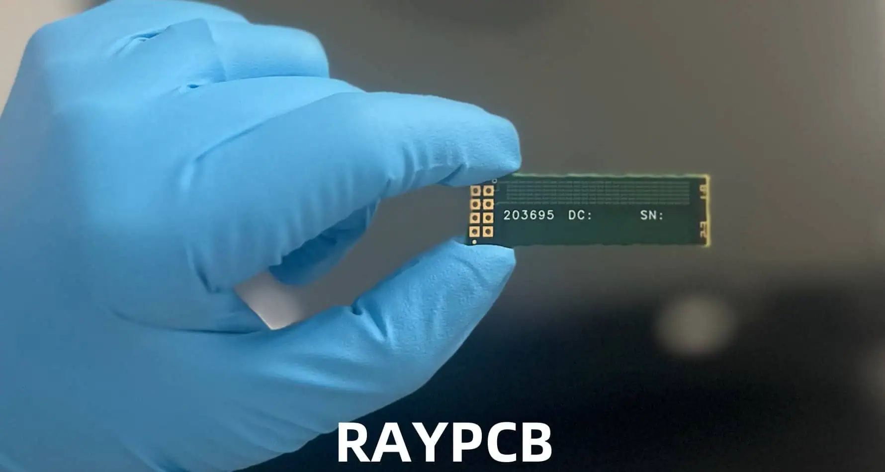
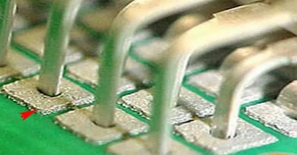
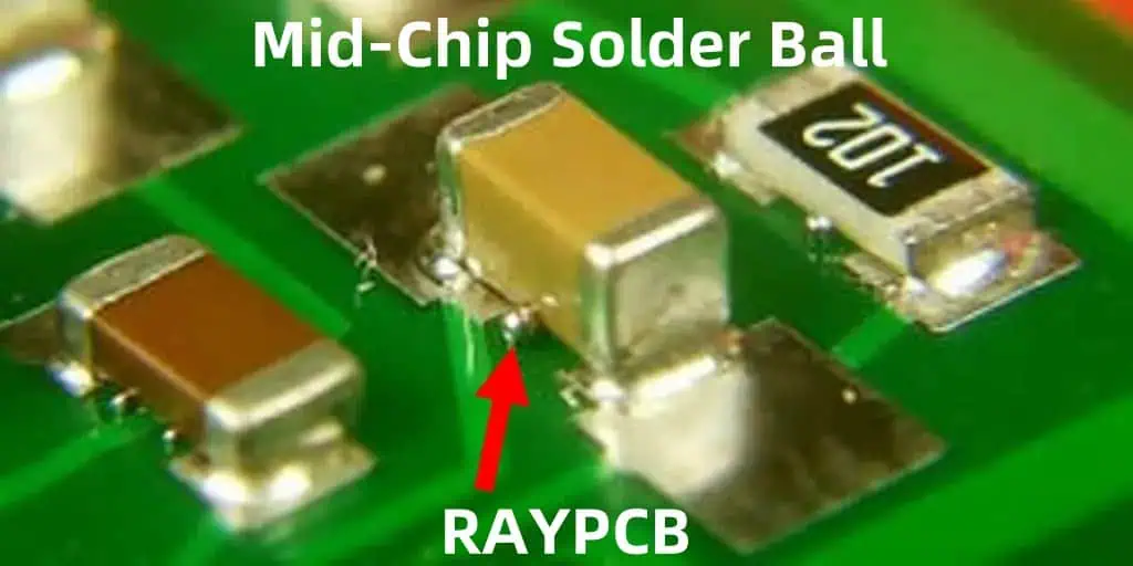
Mid-chip solder balls, also known as under-bump metallization (UBM) or redistribution layer (RDL) balls, are small spheres of solder placed on the active surface of a semiconductor chip. Unlike traditional peripheral solder balls used in ball grid array (BGA) packages, mid-chip solder balls are positioned across the entire surface of the chip, including its central area.
Purpose and Functionality
The primary purposes of mid-chip solder balls include:
- Increasing I/O density
- Improving electrical performance
- Enhancing thermal management
- Enabling advanced packaging techniques
The Evolution of Chip Packaging
Traditional Packaging Methods
To understand the significance of mid-chip solder balls, it’s essential to consider the evolution of chip packaging:
- Through-hole technology
- Surface-mount technology (SMT)
- Ball Grid Array (BGA)
- Flip Chip
The Need for Advanced Packaging
As chip complexity increases and device sizes decrease, traditional packaging methods face limitations:
- I/O density constraints
- Signal integrity issues
- Thermal management challenges
- Size and form factor limitations
Mid-Chip Solder Ball Technology
Composition and Structure
Mid-chip solder balls typically consist of:
| Component | Purpose |
| Solder Alloy | Provides electrical and mechanical connection |
| Under-Bump Metallization (UBM) | Enhances adhesion and prevents diffusion |
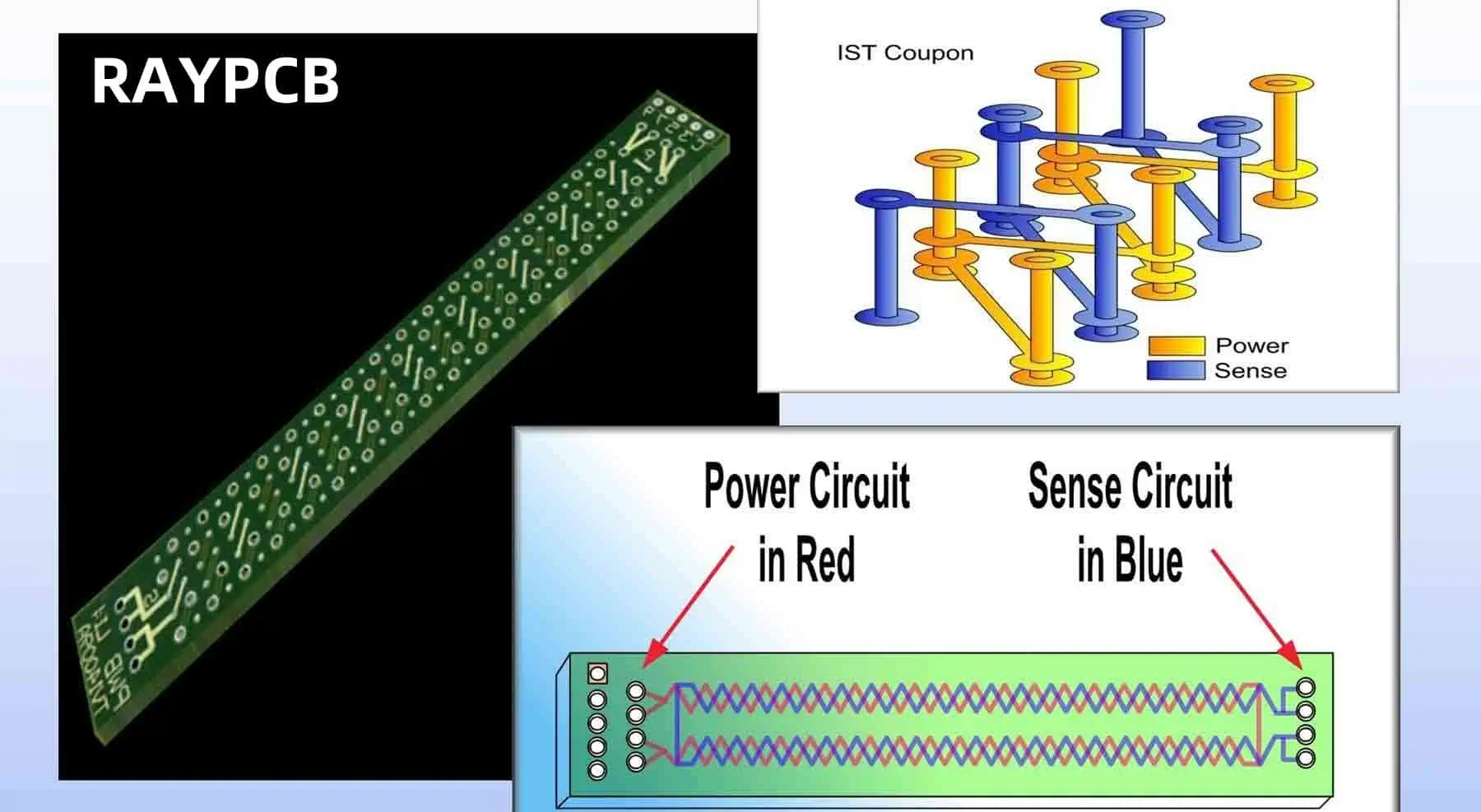
| Redistribution Layer (RDL) | Reroutes chip connections to desired locations |
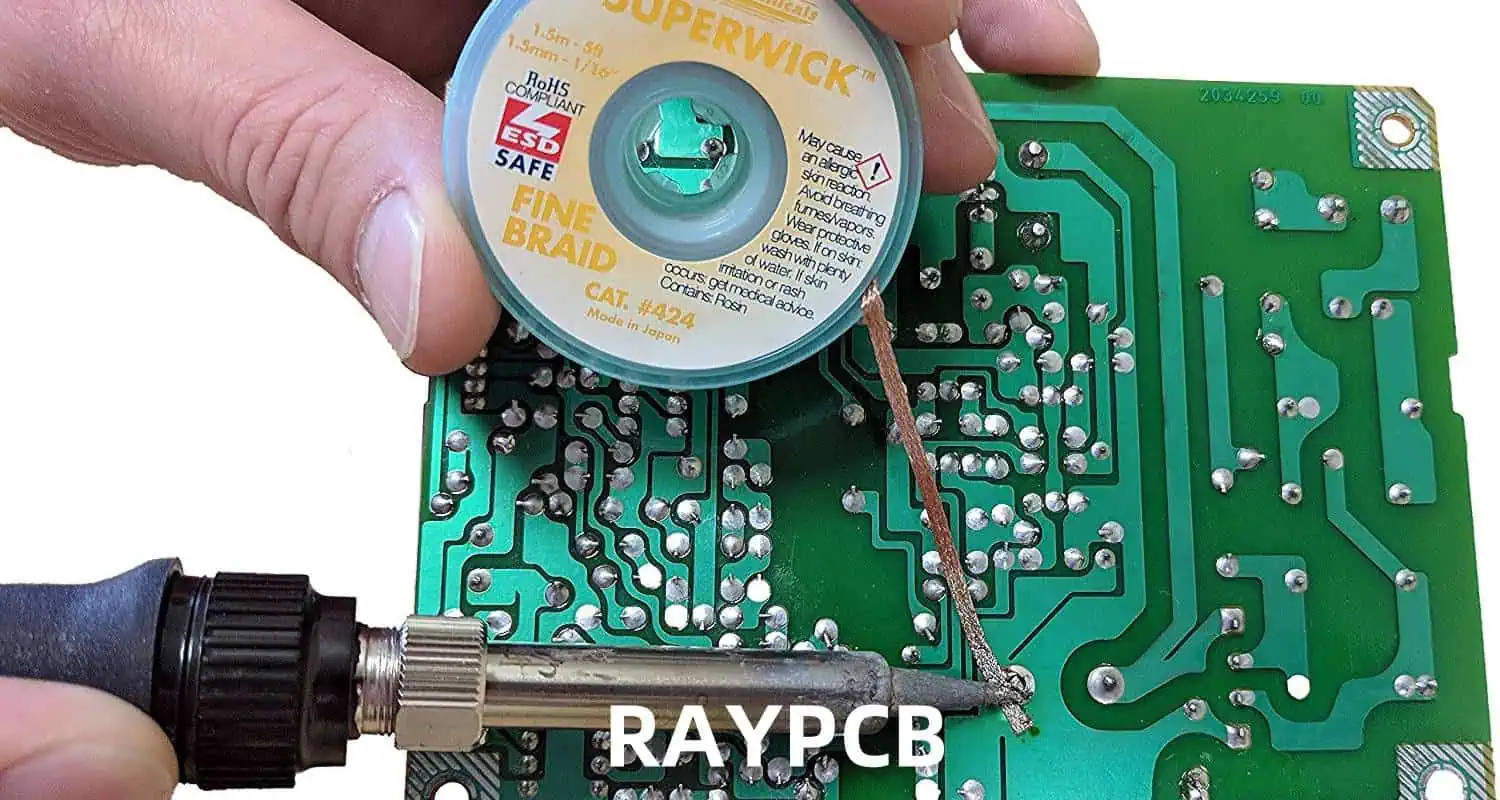
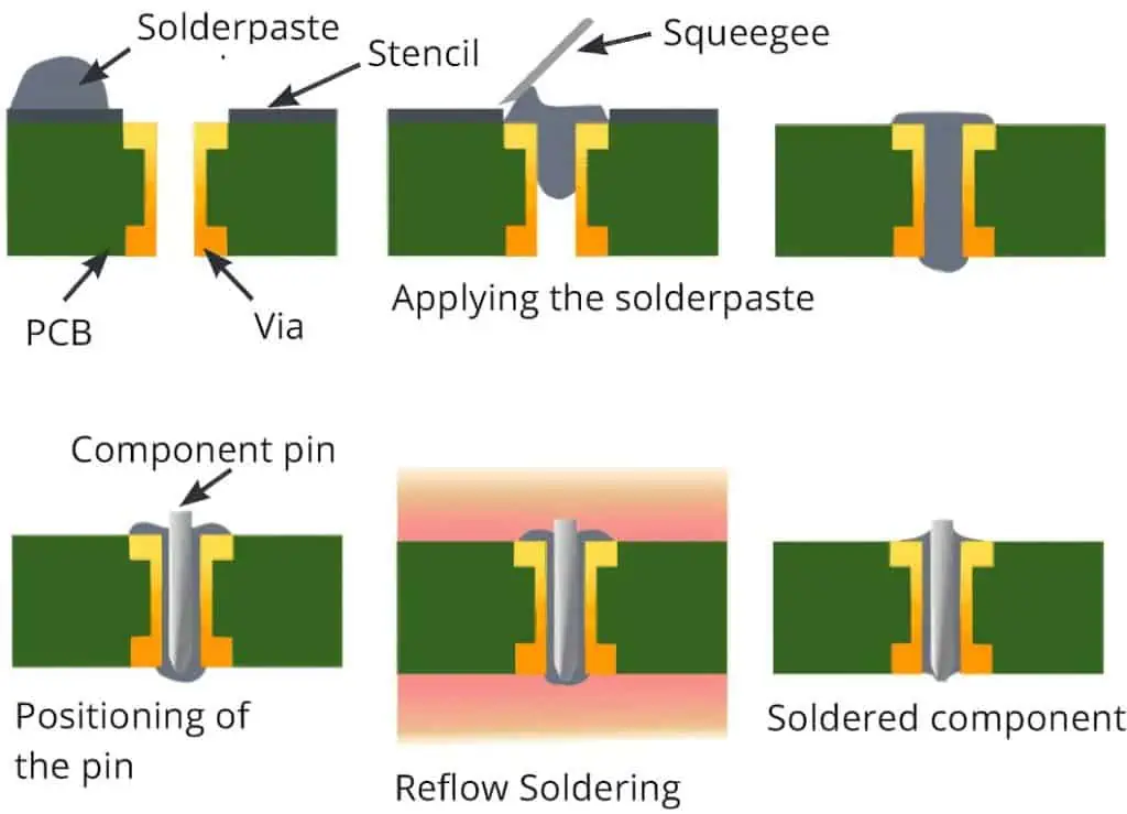
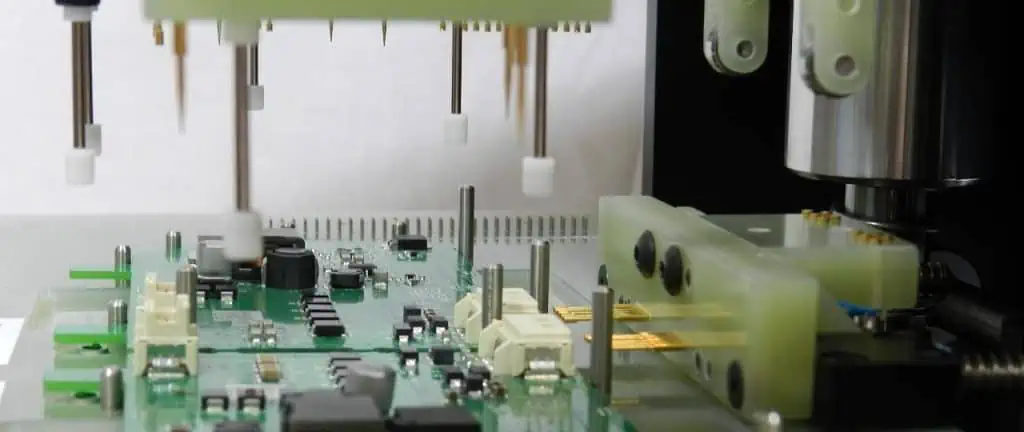
Manufacturing Process
The process of creating mid-chip solder balls involves several steps:
- Wafer preparation
- Redistribution layer deposition
- Under-bump metallization
- Solder ball placement
- Reflow and inspection
Size and Pitch Considerations
Mid-chip solder balls come in various sizes and pitches:
| Feature | Typical Range |
| Ball Diameter | 50-300 µm |
| Pitch | 100-500 µm |
| Ball Height | 50-250 µm |
Advantages of Mid-Chip Solder Balls
Increased I/O Density
By utilizing the entire chip surface, mid-chip solder balls significantly increase the number of possible connections.
Improved Electrical Performance
Shorter connection paths reduce signal delay and improve overall electrical performance.
Enhanced Thermal Management
Mid-chip solder balls can facilitate better heat dissipation from the active areas of the chip.
Enabler for Advanced Packaging
This technology supports various advanced packaging techniques, including:
- 2.5D and 3D IC packaging
- System-in-Package (SiP) solutions
- Heterogeneous integration
Challenges and Considerations
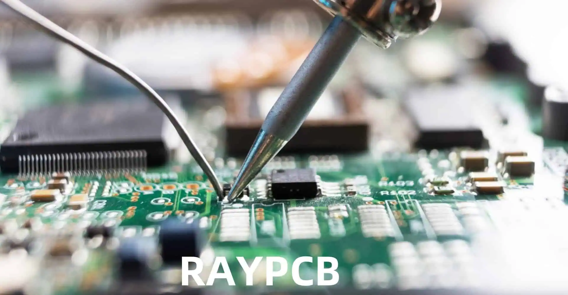
Manufacturing Complexities
Implementing mid-chip solder balls introduces several manufacturing challenges:
- Precise alignment requirements
- Potential for solder bridging
- Increased complexity in inspection and testing
Reliability Concerns
Reliability issues that need to be addressed include:
- Thermal cycling stress
- Drop test performance
- Electromigration risks
Cost Implications
The adoption of mid-chip solder ball technology may lead to:
- Higher initial manufacturing costs
- Increased investment in specialized equipment
- Potential for long-term cost reductions through miniaturization
Applications of Mid-Chip Solder Balls
High-Performance Computing
Mid-chip solder balls are crucial for:
- Advanced CPUs and GPUs
- AI and machine learning accelerators
- High-bandwidth memory interfaces
Mobile Devices
This technology enables:
- Smaller, more powerful smartphones
- Wearable devices with advanced functionality
- Compact IoT devices
Automotive Electronics
Applications in the automotive sector include:
- Advanced driver assistance systems (ADAS)
- In-vehicle infotainment systems
- Electric vehicle power management
5G and RF Devices
Mid-chip solder balls support:
- High-frequency RF components
- Compact 5G infrastructure equipment
- Phased array antennas
Design Considerations for Mid-Chip Solder Balls
Layout and Routing
Designing for mid-chip solder balls requires careful consideration of:
- Signal integrity
- Power distribution
- Thermal management paths
Material Selection
Critical material choices include:
- Solder alloy composition
- Under-bump metallization materials
- Substrate and interposer materials
Thermal Management Strategies
Effective thermal management may involve:
- Strategic placement of thermal balls
- Integration with advanced cooling solutions
- Use of thermally enhanced substrates
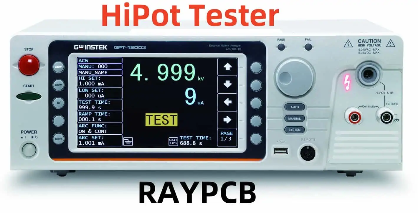
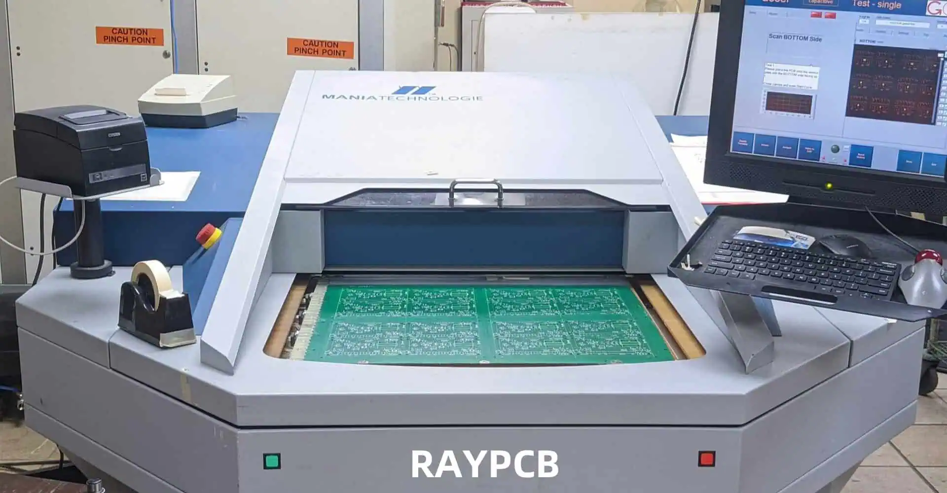
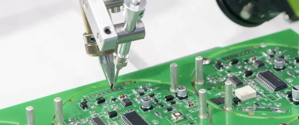
Testing and Inspection of Mid-Chip Solder Balls
X-ray Inspection
X-ray inspection is crucial for:
- Detecting voids and bridging
- Ensuring proper ball alignment
- Identifying hidden defects
Acoustic Microscopy
This technique helps in:
- Detecting delamination
- Assessing solder joint quality
- Identifying internal cracks or voids
Electrical Testing
Comprehensive electrical testing includes:
- Continuity and short circuit tests
- High-frequency performance validation
- Burn-in and stress testing
Reliability and Failure Modes
Common Failure Mechanisms
Key reliability concerns include:
- Solder joint fatigue
- Electromigration
- Intermetallic compound growth
- Thermal cycling stress
Reliability Enhancement Techniques
Strategies to improve reliability include:
- Underfill materials
- Optimized solder alloy compositions
- Stress-relieving package designs
Future Trends in Mid-Chip Solder Ball Technology
Miniaturization
Ongoing efforts focus on:
- Reducing ball size and pitch
- Improving alignment accuracy
- Enhancing inspection capabilities
Materials Innovation
Research is being conducted on:
- Novel solder alloys with improved properties
- Advanced underfill materials
- Environmentally friendly alternatives
Integration with Emerging Technologies
Mid-chip solder balls are being adapted for:
- Chiplets and disaggregated architectures
- Photonic integrated circuits
- Quantum computing devices
Industry Standards and Regulations
IPC Standards
Relevant IPC standards include:
- IPC-7095: Design and Assembly Process Implementation for BGAs
- IPC-A-610: Acceptability of Electronic Assemblies
JEDEC Standards
JEDEC standards addressing this technology:
- JESD22-B111: Board Level Drop Test Method of Components for Handheld Electronic Products
- JESD22-A104: Temperature Cycling
Environmental Regulations
Compliance with regulations such as:
- RoHS (Restriction of Hazardous Substances)
- REACH (Registration, Evaluation, Authorisation and Restriction of Chemicals)
Economic Impact and Market Trends
Market Growth Projections
The mid-chip solder ball market is expected to grow significantly, driven by:
- Increasing demand for advanced packaging solutions
- Growth in 5G, AI, and IoT applications
- Adoption in automotive and industrial sectors
Supply Chain Considerations
The adoption of this technology affects:
- Semiconductor manufacturing equipment suppliers
- Materials suppliers (solder, underfill, substrates)
- Packaging and assembly service providers
Conclusion
Mid-chip solder balls represent a significant advancement in semiconductor packaging technology. By enabling higher I/O densities, improved electrical performance, and better thermal management, they play a crucial role in the development of next-generation electronic devices. While challenges in manufacturing and reliability persist, ongoing research and development efforts continue to address these issues.
As the electronics industry moves towards more compact, powerful, and efficient devices, mid-chip solder ball technology will likely play an increasingly important role. Its ability to support advanced packaging techniques and emerging technologies positions it as a key enabler for future innovations in electronics.
The successful implementation of mid-chip solder balls requires a holistic approach, considering design, materials, manufacturing processes, and reliability testing. As the technology matures, we can expect to see further refinements in ball size, pitch, and materials, along with improved manufacturing techniques and reliability enhancement strategies.
For engineers, designers, and manufacturers in the electronics industry, staying abreast of developments in mid-chip solder ball technology will be crucial for remaining competitive in a rapidly evolving market. As this technology continues to advance, it will undoubtedly open new possibilities for electronic device design and functionality, pushing the boundaries of what’s possible in the world of semiconductor packaging.
FAQ
- Q: How do mid-chip solder balls differ from traditional BGA solder balls? A: Mid-chip solder balls are placed across the entire surface of the chip, including the central area, while traditional BGA solder balls are typically arranged around the periphery. Mid-chip solder balls allow for higher I/O density, shorter signal paths, and better thermal management.
- Q: Are mid-chip solder balls more reliable than traditional packaging methods? A: Mid-chip solder balls can offer improved reliability in some aspects, such as better thermal management and shorter signal paths. However, they also introduce new reliability challenges, including potential issues with thermal cycling stress and electromigration. Overall reliability depends on proper design, materials selection, and manufacturing processes.
- Q: What are the main challenges in manufacturing devices with mid-chip solder balls? A: Key challenges include precise alignment requirements, potential for solder bridging, increased complexity in inspection and testing, and the need for specialized equipment. Additionally, managing thermal stress and ensuring uniform solder ball height can be challenging.
- Q: Can mid-chip solder ball technology be applied to all types of semiconductor devices? A: While mid-chip solder ball technology is versatile, it’s not necessarily suitable or cost-effective for all devices. It’s most commonly used in high-performance applications that require high I/O density, improved electrical performance, or advanced packaging techniques. Simpler, less demanding devices may still use traditional packaging methods.
- Q: How does the cost of mid-chip solder ball packaging compare to traditional methods? A: Initially, mid-chip solder ball packaging can be more expensive due to the need for specialized equipment and more complex manufacturing processes. However, it can lead to cost savings in the long run through increased functionality, improved performance, and the ability to create smaller, more integrated devices. The cost-effectiveness depends on the specific application and production volume.