Applications of a Printable PCB

Rogers RO4835T PCB

If you dismantle an electronic device, you will find a small green board. This board is what we refer to as a printed circuit board. It functions as the life of that electronic device. An electronic or electrical device canโ€™t function without this board.

The green board you see in your electronic device has markings that look like a maze. A printed circuit board allows connections between components. All PCB boards are printable as they allow you to print a specific design on them.

What is a PCB?

A printed circuit board offers mechanical support and connection to electronic components via pads and conductive pads. Furthermore, a PCB features pre-designed copper tracks. These tracks minimize wiring and as such decreases the errors that arise as a result of loose connections.

PCB lays the foundation for the assembly of components. When manufacturing electronic devices, components are usually placed on the bare circuit board. A PCB is a bare board that features pads and conductive tracks. The placement of electronic components like resistors, capacitors, and more makes a PCB a fully assembled board.

What is a Printable PCB?

Rogers-RO4534-pcb

The manufacturing of a printed circuit board goes through several steps. Manufacturers ensure they carefully carry out these steps to achieve a functional board. Printing the design is one of the crucial steps involved in PCB manufacturing. A printable board is a board that has a film which reveals its layers and details.

A plotted printer is used in printing the design of the board. A printable PCB has two ink colors on the layer of the board. The white ink reveals the non-conductive areas while the blank ink reveals the circuits and conductive copper traces. Some manufacturers fabricate printable PCB using specialized PCB 3D printers. These printers are much faster than plotted printers.

Steps Involved in Manufacturing a Printed Circuit Board

Design

Before the manufacturing process commences, you need a design. The design is a blueprint in which the manufacturer begins the process. A computer software application is usually integrated for this step.

Print the design

Creating a design doesnโ€™t just end there. In this step, you will be printing the PCB design with the help of a plotted printer. The PCB will have two different colors of ink.  A clear ink and a black ink. The black ink reveals the circuits and conductive copper traces.

Creating the substrate

In this step, the manufacturer pre-bonds the copper to both sides of the layer. The substrate holds the components. It is the base of the material.

Inner layer printing

Here, the design is printed to the body of the structure, which is usually called the laminate. The photo-sensitive film will harden when you expose it to ultraviolet light. With this, the blueprints and the specific print of the circuit board will be aligned. Also, to aid the alignment process, the manufacturer drills holes in the PCB.

Unwanted copper removal

The PCB manufacturer will need to get rid of unwanted copper from the circuit board. Here, the board is dipped in a chemical solution that gets rid of the unwanted copper.

Inspection

FULL PCB MANUFACTURING Quote

There is a need to inspect the layers to ensure alignment. The drilled holes help in aligning the outer and inner layers. Inspection is necessary to ensure the boards are not defective.

Solder mask application

The panels of the PCB need to be properly cleaned before applying solder mask. The manufacturer then applies the epoxy with the solder mask. An ultraviolet light helps to remove unwanted solder mask.

Silkscreening

This is an important step in PCB manufacturing. Silkscreen prints crucial details on the board. After applying silkscreen, the PCB goes through a curing process and one more coating.

Surface finish

This step involves the application of coating on the board. Surface finishes are available in different types. Coating the board with a surface finish helps in preventing the copper in the printed circuit board from oxidizing.

Testing

An electrical test is usually performed on the circuit board. This helps in confirming the functions of the circuit board.

Applications of Printed Circuit Boards

Copper Coin PCB

Printed circuit boards are applicable across several industries ranging from the medical to military and consumer electronics.

Consumer electronics

Consumer electronics are electronic appliances we use everyday. These include televisions, smartphones, and computers. PCBs play a crucial role in the development of these electronics. Some consumer electronics require the use of advanced PCBs while some require simple PCBs. Circuit boards integrated for consumer electronics should be low-cost.

Automotive components

Automotive parts and components features PCBs. In the past, circuit boards were widely integrated for vehicle parts such as headlight switches and windshield wipers. However, things have changed as PCBs are integrated in advanced features. PCBs are now being used in control systems, sensors, and navigations systems of vehicles. The majority of the systems that regulate the function of a vehicle depend on electronics powered by circuit boards.

Medical devices

There is a growing use of printable PCB in the medical industry. As technology advances, more and more medical devices are being innovated. All these innovations were made possible due to printable PCB. This circuit board is available in medical devices like infusion pumps, medical imaging systems, internal devices, and monitors.  PCB manufacturers need to pay attention to the PCBs used in the production of medical devices. These boards must meet some strict standards to ensure safety.

Aerospace components

Aerospace devices are usually exposed to harsh weather conditions. Therefore, high-end PCBs are widely integrated for the manufacturing of these devices. Printable PCBs are a core component in power supplies, communication equipment, and monitoring equipment used in the aerospace industry. These boards are necessary for the development of aerospace components.

Conclusion

PCB lays the foundation for the assembly of components. When manufacturing electronic devices, components are usually placed on the bare circuit board. A PCB is a bare board that features pads and conductive tracks. The placement of electronic components like resistors, capacitors, and more makes a PCB a fully assembled board. Printed circuit boards are applicable across several industries ranging from the medical to military and consumer electronics.

Unnoticed Uses and Making of 100K Resistor

100K-Resistor

You may have heard of resistance. It disrupts the electrical current. As the word suggests, the main purpose of the resistor is to reduce the flow of current, divide voltage and adjust the signal level. The electric resistance is measured in Ohms. When it comes to resisting current, we have several types of resistors, from wire wound resistors to thermistors. Letโ€™s dig deeper to know more about the 100k resistor and what are its uses, and how it is different from the rest of the resistors.

What is a 100K Resistor?

As the name suggests, the 100K resistor constitutes 100,000 ohms of resistance. When compared to the other resistors, a 100K resistor is the uppermost limit of the resistors that companies around the world make.

 What Is The Color Code of the 100k Resistor?

10k ohm

Color code is the identification of any resistor. A layman may consider it some ordinary line on a resistor. A circuit designer or electrical engineer knows well the purpose of these lines. Color codes have some values and help to calculate the resistance of the resistor.

The color code for a 100k ohm resistor is Brown, Black, Yellow, and Gold. Let me explain to you the first band is brown, and the second band is yellow. Both show digit values one and zero, respectively.  The gold band on the resistor represents the tolerance value. It means that the tolerance value may go up and down to five percent.

Uses of 100K Resistors

There are a number of uses for 100K resistors, such as:

1. Voltage Divider and time Circuits

Firstly, one common use for 100K resistors is in voltage divider circuits.  They divide the voltage properly. Similarly, time circuits also have 100k resistors. One popular example of a timer circuit is the 555 timer circuit. 100k resistor helps to delay the current flow in some circuits. It is the need for the circuit in a particular device. That’s why 100k resistors are most popular as voltage dividers and time delay circuits.

  • Biasing Transistors

Another common use for 100K resistors is in biasing transistors. Biasing refers to the process of setting the voltage levels at the transistor’s input and output terminals so that it operates in the desired way. 100K resistors are helpful in biasing circuits to help set these voltage levels.

3. Current Limiting

Additionally, 100K resistors serve a lot in limiting current. As a result, 100K resistors frequently serve as current-limiting resistors for LEDs to prevent them from burning out due to excessive current.

4. LED Current Limiting

The engineers use 100K resistors to limit the current flowing through LEDs. In order to prevent LED burnout due to excessive current flow, a current-limiting resistor is required. Sometimes delicate parts burn due to the heat of electric current.

5. Oscillators

100K resistors are in practice in oscillator circuits. 100k resistors work best in combination with capacitors and other components. So, Oscillators help generate a periodic waveform,

  • Voltage Regulators

ย A voltage regulator helps to regulate the voltage of a power supply or battery. 100K resistors in voltage regulator circuits help set the output voltage of the regulator. 100K resistors serve the purpose best in voltage regulators.

Making a 100K resistor requires some knowledge of electrical circuits and some basic materials. However, it’s important to note that making your own resistors is not recommended for most applications. A layman doesn’t have proper knowledge of parts placement. ย ย That’s why commercially available resistors are typically more precise and reliable. Itโ€™s hard to do proper testing of DIY resistors. However, letโ€™s have a look at the making of the resistor.

How to Make a 100K Transistor?

FULL PCB MANUFACTURING Quote

To make a 100K resistor, you will need a length of wire with a specific resistance per unit length. The resistance per unit length of wire is typically given in Ohms per meter or Ohms per foot.

Once you have the correct length of wire, you will need to wind it into a specific shape to create the resistor. One common way to do this is to wind the wire around a ceramic or other non-conductive core, such as a pencil or small tube. The number of turns and the spacing between the turns will depend on the desired resistance and the diameter of the core.

After winding the wire into the desired shape, you will need to measure the resistance of the resistor using a multimeter or other measuring device. It’s important to note that the resistance of homemade resistors may not be as precise as commercially available resistors and may vary depending on the specific wire and winding technique used.

Making your own 100K resistor is possible but not recommended for most applications. It requires a specific length of wire with a specific resistance per unit length, as well as knowledge of basic electrical circuits and some basic materials. Commercially available resistors are typically more precise and reliable. Thatโ€™s why engineers go for these resistors.

 Why Are 100k Resistors Most Suitable As Compared To Two 50k Resistors In A Series?

You can use two 50 k resistors instead of a single 100K resistor. Sometimes this practice doesn’t provide you suitable power rating for the application. The second thing is that stray capacitance or inductance may increase due to using two 50k resistors. That’s why a 100k resistor serves best for the purpose. Another thing is that if connecting the different resistors in series can serve the purpose, then why manufacturers are making different resistors of different resistance? Manufacturers are making resistors of some specific resistances to avoid stray capacitance or inductance issues. Thatโ€™s why a single 100K resistor serves best and is necessary for several circuits. Two 50k circuits cannot full fill the purpose.

Final Note

So, thatโ€™s it with the 100K resistor. Its high resistance makes it suitable for multiple uses. It is possible to use a 100K resistor in several ways, and it contains 100,000 ohms of resistance. We tried to cover the topic from all perspectives. Feel free to share your thoughts with us.

Is IR Reflow Superior to Vapor Phase Reflow?

IR Reflow

Our company has been constantly searching for cutting-edge technology that can speed up assembly while enhancing PCB quality. The IR reflow, which has to do with the profiling of each Circuit board type and took a significant period of time, was included among the assembly line’s bottlenecks.

Vapor Phase Reflow was discovered in our quest to increase the efficiency of the surface mount assembly process, and investing in these devices and systems has successfully eliminated delays. Here, we contrast the two soldering techniques.

Soldering Using IR Reflow

A typical technique for the quick manufacturing of PCBs is IR reflow soldering. The solder paste, made of solder flux and solder, is applied to the essential parts of the circuit board during the procedure. There is a minor viscosity to the paste. Electrical components must stick to the board as a result of this.

The PCB goes through the oven while being reflow soldered. This solder paste melts as a result (reflow). Each circuit board passes through a cooling cycle after its oven stage. These electrical components are now permanently attached to the pcb board because the solder has set.

For a few reasons, reflow soldering can be frequently used in the manufacture of circuit boards. The oven technique, in particular, has a far higher soldering capability than the hand soldering. That capability permits the manufacturing of the circuit boards in a large volume very quickly.

Second, there has been number of improvements made to ir reflow soldering techniques throughout time. These developments have made it possible for reflow soldering to produce surface mount devices with soldering of the greatest quality.

HACR Procedure

IR Reflow wave

To achieve uniform soldering throughout the board when employing the IR reflow method to solder the PCB assembly, a special reflow profile must be created. HACR procedure primarily utilizes hot air, which isn’t always an appropriate method for soldering.

The HACR profile is significantly influenced by the PCB’s thermal mass as well as the components present on it. In addition, the components’ color also affects the profile since darker colors absorb heat faster and readily than lighter or reflective colors.

These elements alter the pace at which heat is transferred from hot air immediately it circulates inside the oven.

Thermocouples are used on the test circuit assembly to measure the temperature change as it passes the oven during profiling. This approach has two shortcomings. The first disadvantage is that it takes time to complete the task because a specific temperature profile is required for uniformly proper soldering. A second problem is that if a limited run is involved, the buyer might not be ready to deliver the necessary test PCB assembly.

VPR Procedure

Vapor phase oven use the vapor layer that transfers the latent heat when it condenses, in contrast to HACR, which utilizes hot air for transferring heat into the PCB as well as its components since it moves through a system present on the conveyor belt. When a particular liquid is boiled at a temperature of 235 ยฐC within the system, a vapor layer is produced, and the latent heat gotten from this vapor is transferred very effectively, causing components with differing thermal masses to reach this very same temperature simultaneously.

Early VPR oven models were not known since a lot of this vapor leaked out, making them harmful to both the user and the environment. Moreover, its IR reflow profile was fairly dependent on the temperature range and the volume of fluid inside the tank.

Only few batches of PCB assemblies could be soldered at once due to the need for manual handling when putting them inside the oven.

Current VPR ovens have a completely new design, with this enclosure recovering nearly all of the vapor medium. The manufacturers now handle PCB assemblies automatically, making it possible to precisely monitor and regulate its temperature profile.

VPR Soldering Process

FULL PCB MANUFACTURING Quote

Since all that is required to melt its solder is the introduction of sufficient heat, soldering first appears as a straightforward procedure. Whenever the system uses solder paste for soldering SMT boards, there are many more steps involved in the process.

A copper pad just on Circuit board as well as component leads must also warm up to a temperature just above the solder paste’s melting point in order for a solder joint to be considered successful. A chilly and unsuccessful joint arises from failing to accomplish this. Also, the components should not be overheated when applying heat because this could harm them. In contrast to other soldering methods, such as radiation, forced convection, or conduction via the soldering gun, this VPR process of soldering transmits heat from the condensing vapor.

The VP reflow machines operate in a very basic manner. This vapor stage fluid sits at room temp at the fluid tank’s bottom before being turned on.

The fluid is heated to boiling after being turned on at 235 ยฐC, which is the average melting temperature of the lead-free solder pastes.

The ideal temperature necessary for melting the solder paste is 235 ยฐC, hence VPR system manufacturers explicitly engineer their products to have a boiling point for a liquid in vapor phase at this temperature. The vapor produced by the boiling liquid is thick and has sufficient latent heat to be transferred to the circuit board assembly.

Vapor condenses present on the cold circuit board assembly as it enters the tank, transmitting the latent heat into the circuit board pads and components till they all reach the equivalent temperature like the vapor. The circuit board assembly cannot become too hot due to the system.

Conclusion

For IR reflow soldering, the solder paste, made of solder flux and solder, is applied to the essential parts of the circuit board during the procedure. Vapor phase type of reflow soldering is a quick and incredibly reliable technique that our company recommends for circuit board assemblies. The technique is appropriate and dependable for soldering SMT circuit boards with a variety of complicated components, including flip chips, QFTs, ceramic assemblies, and BGAs.

Lead Free Solder Vs Lead Solder: Which is Better?

lead free solder

For so many years, the leaded solder is now the material of choice for PCB manufacturing. However, in recent years, consumers worry about the environmental and health implications of these leaded products, which has increased. These factors led to the European Union’s RoHS directive, which restricted the use of hazardous materials in electronic and electrical equipment, to take effect starting July 2006.

Some nations, unlike the U.S.A, do not have legislation that makes the use of lead within consumer products unlawful. But, some companies are requesting that the electronic device they order be made with lead solder. But again, what type of solder is recommended for usage in the electrical industry? What distinguishes lead free solder from solder that contains lead?

This piece will find answers to all questions relating to this, coupled with providing additional insights regarding lead free solder and leaded solder.

What is Lead Free Solder vs Leaded Solder?

lead free SMT solder

Solder is typically used by electronic makers to attach components to Circuit boards. All solders, whether lead free solder or with lead, have the same purpose. However, different solder techniques are used with different devices as well as use situations.

Lead Soldering

Lead and tin are the two main ingredients in leaded solder. Leaded solder’s sufficient flowing capability is a benefit. Since its melting point is lower than that of lead free solder, it doesn’t heat up components as much.

Moreover, lead free solder takes on a duller appearance whenever it cools, making it harder for users to spot problems like oxidation. Lead solder also is less expensive and simpler to use compared to lead free solder.

Lead Free Solder

The elimination of lead from electronics manufacturing as well as waste recycling procedures is the primary driver behind manufacturers’ switch to the usage of lead free solder. Alternative materials for soldering centered on the tin metal have rapidly developed over the past 20 years in the field of electronic manufacturing. The components used in this alternate method have characteristics that are different from those of the tin and lead eutectic composition.

Soldiers require performance akin to that of superalloys used in jet engines because they are functional around 80% of the melting temperature. But as things get smaller, the demands for solder junctions keep going up because to the rising stress and density characteristics. Hence, the PCB design that takes into account its melting point that is high and anisotropic features is required for lead free solders.

The Differences Between the Features of Lead and Lead Free Solder

FULL PCB MANUFACTURING Quote

When lead is used in large quantities for a long period of time in consumer goods, negative consequences on the environment, as well as on human health, results. Nowadays, businesses use lead free solder to assist the social responsibility initiatives of environmental protection.

The Melting Point of Lead Free Solder Is Greater than the Lead Solder

Lead-filled solder melts at a temperature of 1830ยฐC, whereas lead free solder melts at 2170ยฐC. The consequences of lead free solder’s greater melting point are as follows:

Compared to lead soldering, which uses a lower temperature, lead free soldering quickly oxidizes its solder. Certain components, such as those with plastic packaging as well as electronic capacitors, are adversely impacted by the higher soldering temperature that lead free solder has.

Components with a low dielectric are more prone to failure because of the high component stress caused by lead-free solder’s high temperature.

Components made with lead free solder feature a number of soldering surfaces. Tin is frequently used by businesses on these surfaces due to its affordability. However this tin produces a thin layer of oxidation present on the exterior that can result in electroplating.

Whether eutectic

Because lead and tin combined to make an eutectic mixture, manufacturers valued this combination. What we mean is that this temperature of the tin and lead alloy is lower than the heats of the two metals separately. Although a eutectic metal pair has not been found, a successful lead free soldering method has been developed by electronic manufacturing industry.

Health Issues

Businesses concerned with environmental preservation cite lead’s harmful nature as this primary justification for switching to lead free soldering. The human body can indeed collect lead even after brief, repeated exposures. Lead can also easily enter the body via your mouth, nose, or skin. Lead-free fuel and paint are now both commonplace. Yet, one of the last remaining products which still uses it is solder.

Workers are especially susceptible to the risks of lead because they can swiftly breathe it in or receive it by contacting contaminated surfaces inside a sector with high lead output. Keep in mind that lead poses a greater risk to youngsters. Thus, everywhere you use lead solder, consider these health issues seriously.

Cost

Compared to lead free solders, lead-filled solder is less expensive. This is due to the fact that lead costs just one-tenth as much as tin, making lead based solder very accessible. Lead free solders can also be made more expensive by some manufacturers who swap out the tin for silver.

Lead Free Solder has Poorer Wettability Compared to Leaded Solder

When the solder joint’s wettability is low, it struggles to meet the needs of tensile strength, shear capacity, and self-regulation ability. As a result, low wettability leads to a high solder joint rejection rate, especially when changes aren’t made to address this weakness.

Physical Characteristics: Lead Free Solder vs Lead Solder

Joint reliability is negatively impacted by lead free solder. Lead free solder is superior to leaded solder in terms of mechanical effect.  Moreover, lead-free solder develops surface oxides, the flux impurities, as well as alloy deposits which can result in subpar performance in terms of contact resistance. As a result, the switch in electronic production from the lead to the lead-free does not completely replace the mechanical and electrical components.

Adopting Lead Free Solder

It is crucial to understand that the main distinction between lead free and lead-lead solder is its high tin content. This will help you decide which solder type to use. As a result, you should consider the following factors before making your decision.

Metal dendrite growth

It is significant to notice that the growth processes of tin whisker and metal dendrite differ. Ionic electro-transfer during electrochemistry results in the formation of metal dendrites. Tin whisker, on the contrary, creates shortcuts which further cause circuit failure.

Growing of Tin Whisker

Tin whisker, acting in cylindrical filament or columnar nature, emerges from susceptible areas of the tin oxide covering. There may be shortcuts created by the whisker in-between neighboring pins. Furthermore, it could impact the high-frequency components negatively.

One primary cause of tin whiskers is pressure stress that is present in tin soldering coatings. For example, when there is an excess of metallic alloy Cu6Sn5, it can lead to a number of defects, including build up of pressure stress upon that tin coat, CTE mismatching, as well as pin distortion, which further results in the development of the tin whisker.

Tin whisker, that is more obvious in purest tin, is another effect of high tin alloy concentrations. Fortunately, a number of metal alloys, including Bi and PB, can stop tin whisker formation.

CAF Creation

Another failure brought on by electrochemical processes is a CAF – conducting anodic filament. CAF development is triggered by anode conductive filaments that contains some copper and grows from positive electrodes to negatively charged electrodes. This circuit board is where the procedure takes place.

When the negative and positive electrodes are connected via a short circuit, CAF typically increases. This results in a terrible catastrophe for the production of extremely compressed PCBs. Lead free solder’s high melting point hastens CAF generation.

Tin Pest

Tin pests are a result of impulsive polymorphism stage modification. Normally, uncontaminated tin would turn from white color to grey at temperatures below 130C. Tin pests should ideally pose a risk to reliability. Yet, because the pollution and iron combine, you won’t usually notice it.

Lead-free Solder vs Lead Solder: Which is More Suitable for Use?

Aerospace Corporation conducted a study regarding the use of lead in consumer electronics, which is at odds with the environmental and health facts about leaded electronics. According to this study, there is insufficient evidence to back up the claim that lead used in electronic devices seriously harms both humans and the environment. The quantity of lead which manufacturers really use in electrical rework is so negligible as to not endanger animals.

If lead solder is offered in your local markets, use it. It is simpler to use, its melting point is lower, and results in fewer joint quality issues.

Conclusion

Leaded solder has a lot to offer the electronic manufacturing industry, but change is sweeping in. If they haven’t already, all industries that utilize a lot of solder will most likely switch to the lead free soldering shortly. Aside from that, as many governments implement eco-friendly policies, there could not be enough solder available in the marketplace for hobbyists.

With every change, lead free solder encounters resistance from some people. Yet, in terms of protecting human safety and health, a switch to a much safer approach is unquestionably important.

What Does Arduino Sensor Humidity Entail?

Arduino Sensor Humidity

The glass substrate, the lower electrode, the humidity-sensitive material, as well as the upper electrode make up the majority of humidity sensor. These two lower electrodes, the humidity sensitive material, as well as both capacitors created by the upper electrodes are all connected in the series form. A large molecular polymer called a humidity-sensitive substance alters its dielectric constant depending on the environment’s relative humidity.

When the relative humidity varies, its humidity sensor capacitance also changes, and vise – versa, the humidity sensor’s capacitance adjusts to the change in environmental humidity (the capacitance usually falls within 48 to 56 pf). This humidity-sensitive capacitance adjustment is converted by the conversion circuit of the sensor into a change in voltage that reflects a relative humidity change from 0% to 100 percent RH, as well as the sensor’s output changes in a linear way from 0v to 1v.

Typical Arduino Humidity Sensors

Arduino Sensor Humidity PCBA

The most popular humidity sensors that are appropriate for Arduino projects are included in this section.

The most often used humidity sensor is from the DHT series. All of them feature automated calibration, are really simple to use, as well as contain the Arduino software libraries, which is well-liked by makers. Let’s examine DHT11’s capabilities.

Old DHT11

  • For the DC operating voltage, it has a value of 3.3 to 5.5 volts
  • In addition, its range of temperature falls between 0 to 50 ยฐC
  • The Range of Humidity falls between 20 to 95% RH
  • Its Temperature Accuracy falls within ยฑ2โ„ƒA
  • Also, its Humidity Accuracy falls within ยฑ5%RH
  • Type of Sensor:  Sensor for resistive humidity

The DHT11 has a limited measurement range as well as low measurement precision frequently applied in several student projects. There’s an upgraded version of the DHT11, which is wonderful news.

The resistive humidity sensors were replaced by the capacitive humidity sensors by the manufacturer, and the upgraded DHT11 has considerably better measurement range.

Recent DHT11

Here, electrical resistance across two electrodes is measured by the DHT11 in order to identify water vapor. A moisture-holding substrate having electrodes placed onto the surface serves as the humidity sensor component. Ions are generated by a substrate whenever water vapor gets absorbed by it, increasing the conductivity in between these electrodes.

  • For the DC operating voltage, it has a value of 3.3 to 5.5 volts
  • In addition, its range of temperature falls between -20 to 60 ยฐC
  • The Range of Humidity falls between 5 to 95% RH
  • Its Temperature Accuracy falls within ยฑ2โ„ƒ
  • Also, its Humidity Accuracy falls within ยฑ5%RH
  • Type of Sensor:  Sensor for capacitive humidity

DHT22

FULL PCB MANUFACTURING Quote

The top-tier DHT22 model, also referred to as RHT03 or AM2302, is part of DHT series. Both its measuring range as well as high accuracy in measurement is very broad.

  • For the DC operating voltage, it has a value of 3.3 to 5.5 volts
  • In addition, its range of temperature falls between -40 to 80 ยฐC
  • The Range of Humidity falls between 0 to 99.9% RH
  • Its Temperature Accuracy falls within ยฑ0.5โ„ƒ
  • Also, its Humidity Accuracy falls within ยฑ2%RH
  • Type of Sensor:  Sensor for capacitive humidity

DHT22 can be employed in the meteorological, medical, as well as different professional fields. It also has superb long-term stability.

AM2311A

A humidity and temperature compound sensor with a calibrated signal output is the AM2311A humidity and temperature module. In order to ensure the product does have very high dependability and great long-term stability, it uses sophisticated digital acquisition technology as well as humidity and temperature monitoring technology.

  • For the DC operating voltage, it has a value of 3.3 to 5.5 volts
  • In addition, its range of temperature falls between -40 to 80 ยฐC
  • The Range of Humidity falls between 0 to 99.9% RH
  • Its Temperature Accuracy falls within ยฑ0.5โ„ƒ
  • Also, its Humidity Accuracy falls within ยฑ3%RH
  • Type of Sensor:  Sensor for capacitive humidity

How to Select the Most Effective Arduino Sensor Humidity

Arduino Sensor Humidity Design

Large performance and price discrepancies exist between various humidity and temperature sensors. How then should you select the best sensor to suit your projects?

Measure Range

The range of measurement must be established prior to choosing any humidity sensor, just like with temperature and weight measurements. Humidity and temperature control and measurement typically do not call for full humidity (which is 0 to 100% RH) in measurement, with the exception of scientific and meteorological research departments. Choose a range which best suits the needs of your project because, broadly speaking, the greater the range, the more expensive it will be.

Accurate Humidity

The humidity sensor’s most crucial indicator is measurement accuracy. This humidity sensor advances one level or a grade per each increase in percentage point. Its manufacturing costs as well as selling prices differ wildly because varied precisions must be attained. The DHT11 protocol is enough for most tasks. The 5โ€“95% RH measuring range would satisfy majority of applications out there.

What are the Uses of the Arduino Sensor Humidity?

Monitoring the climate

For the purposes of scientific research, military operations, and agricultural and industrial production, weather observation as well as forecasting are extremely important. Thus, humidity sensors serve as a crucial piece of equipment for humidity measurement. For instance, the meteorological balloon measuring equipment for humidity has utilized resin swelling sensors for humidity.

Greenhouse Breeding

There are many greenhouses in the modern forestry, agriculture, as well as animal husbandry businesses. The greenhouse has to control its humidity just as much as its temperature. One requirement for lowering pests and illnesses and raising output is controlling humidity inside a range that is favorable for the development of crops, livestock, trees, and poultry.

Industrial production

Air humidity has a direct impact on product output and quality in the electronics, textile, precision machinery, ceramics, and other industries, so it needs to be adequately controlled and managed.

Conclusion

It’s quite simple to include temperature and humidity data to the DIY electronic applications when utilizing an Arduino sensor humidity. It is ideal for outdoor weather stations, indoor climate management systems, including garden or farm monitoring systems.

Top Semiconductor Chip Manufacturers in the World

manufacture semiconductor

As the world becomes more digital, devices are now assisting us to carry out our daily activities. Therefore, semiconductor chips are becoming smarter, faster, and smaller. This makes it easier to carry out analog tasks digitally. Cars are becoming electric, humans activities are carried out digitally, and commerce is becoming digital

Semiconductors play a key role in the technology world and the modern economy at large. These very tiny electronic circuits are the brain of millions of devices. Even the most powerful and most advanced device features semiconductors. Machines and devices like space vehicles, medical equipment, car computers, and smartphones among others feature semiconductors. As the use cases of semiconductors continue to increase, the manufacturing of semiconductors keep improving and manufacturers keep prospering.

The semiconductor chip industry is indeed a competitive one as semiconductor chip manufacturers keep producing faster, smaller, and more powerful semiconductor chip. Semiconductors are in four primary categories which include commodity integrated circuits, microprocessors, systems on a chip, and memory chips. The semiconductor industry keeps growing at a gradual pace since the advent of the microchip. Here, we will have an indepth study of the semiconductor industry and the manufacturers there.

What are the Functions of a Semiconductor Chip?

us semiconductor companies

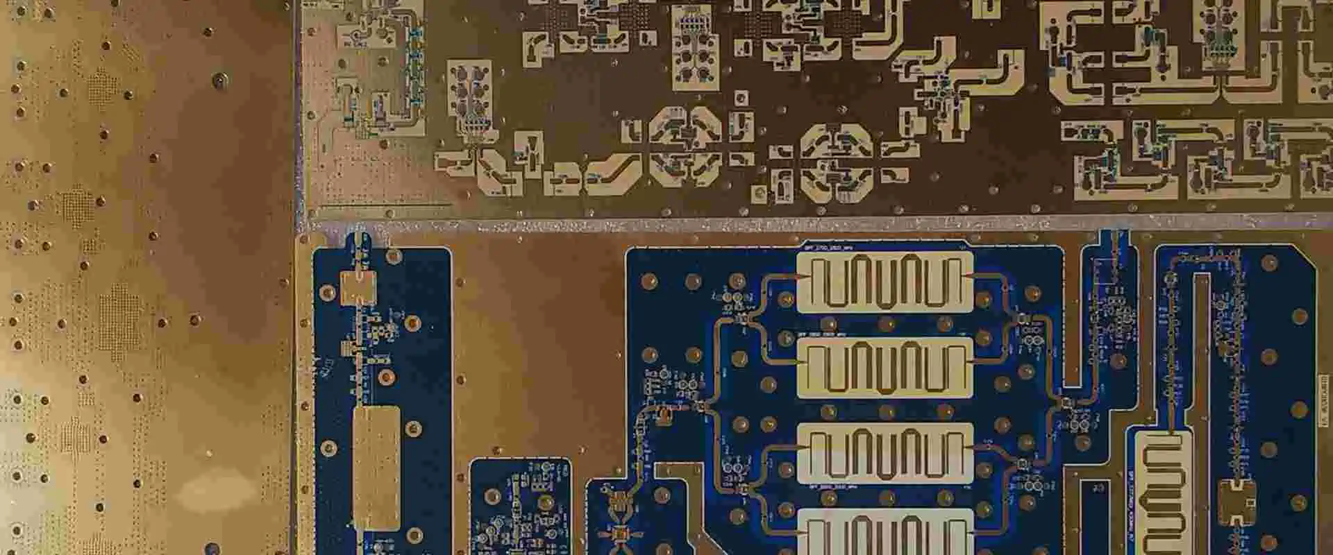
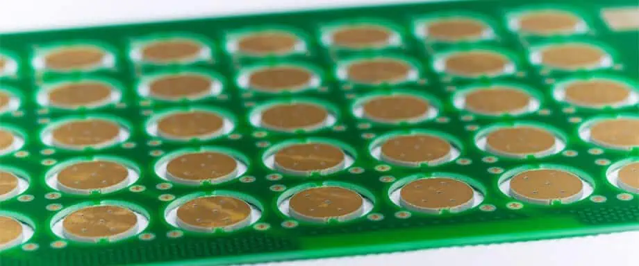
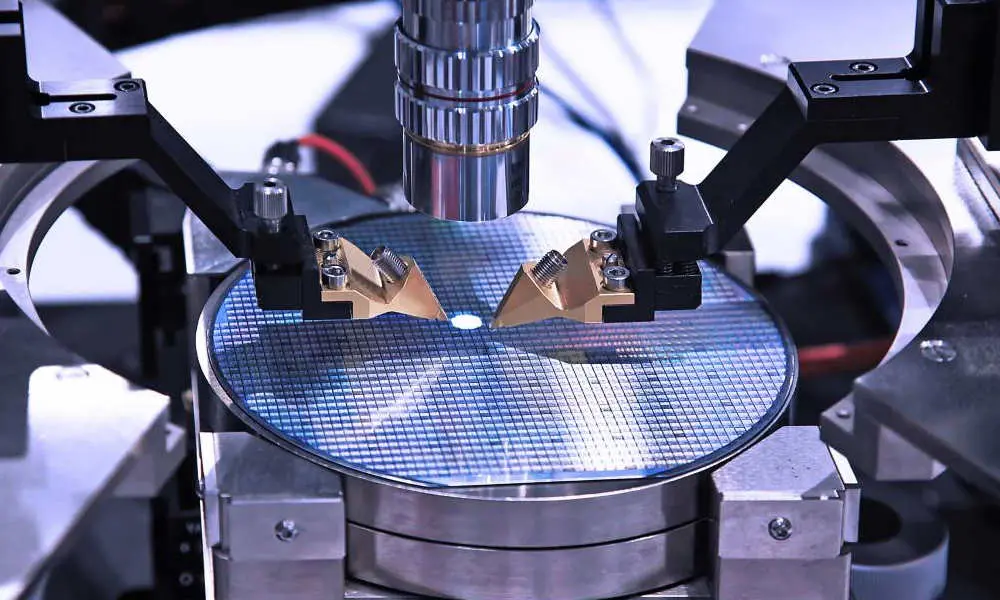
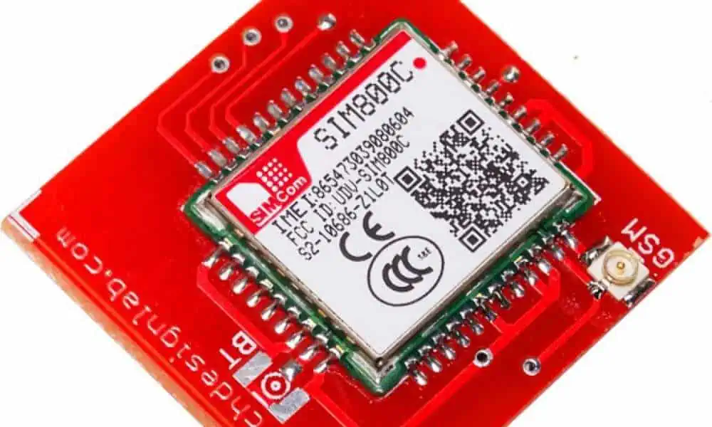
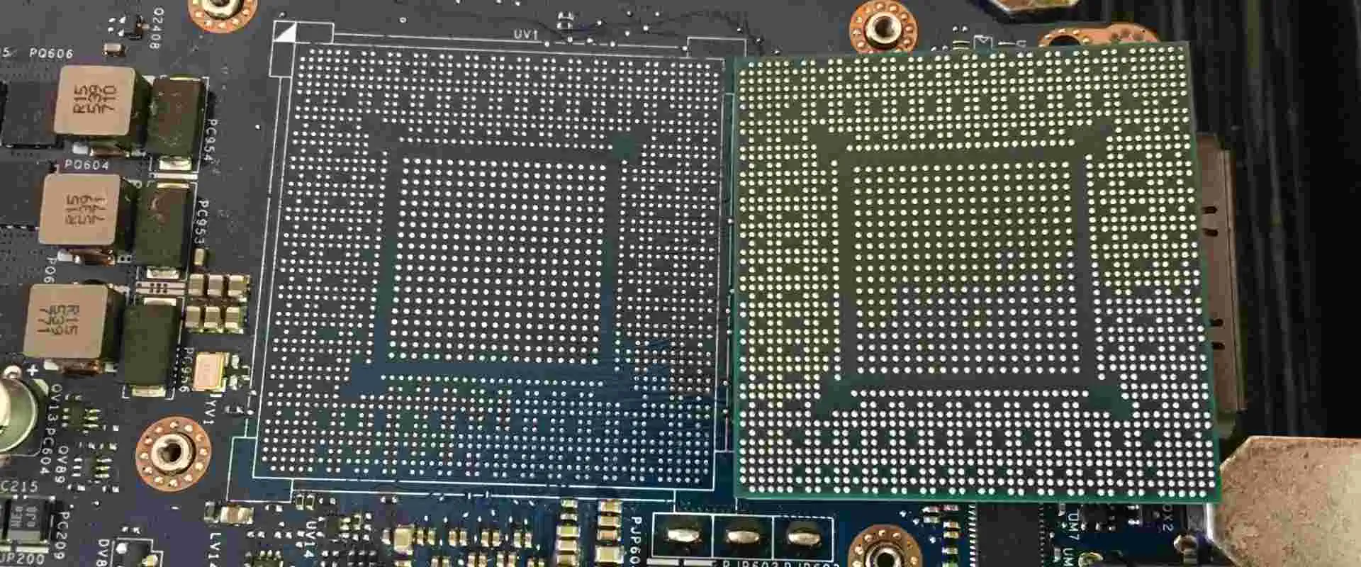
A semiconductor chip serves as the foundation for electronic devices. This chip is also known as microchip or integrated circuit. It is usually made from materials like silicon or germanium. Semiconductor chips are known to play a crucial role in the manufacturing of electronic devices. Therefore, these chips are an important aspect of our daily lives.  

The semiconductor technology has experienced developments and growth for the past 50 years. This growth and development have resulted in the manufacturing of more reliable and powerful electronic devices. A semiconductor chip features many transistors. This chip is around us. It is available in the computer used in conducting businesses, the mobile phones used in communicating, and the vehicles that transport us from place to place.

Also, these chips are available in the machines that treat diseases, the electronic gadgets we use in playing games, and more. Semiconductor chips donโ€™t just make it possible to produce these electronic devices, they are responsible for the compactness and functionalities of these devices.

Which Industries Integrate Semiconductors?

Semiconductor chips are widely integrated across several industries. A lot of industries rely on this small and powerful chip. Examples of these industries include:

Telecommunication

Semiconductor chips control the functions of telecommunication devices. A wide range of technologies rely on telecommunication semiconductors.

Consumer electronics

The washing machine, refrigerator, air conditioner, and microwaves in our homes feature semiconductor chips. These chips control timers, temperatures, and other parameters.

Healthcare

Semiconductor chips are available in machines used in the healthcare system. These machines have reduced the risk associated with surgeries. Also, they have made surgeries safer since they operate with a high level of precision.

Computing

Microchips are widely integrated in computers. Based on the chip type, a semiconductor chip makes use of binary code to carry out the commands you give.

Top Semiconductor Chip Manufacturers

FULL PCB MANUFACTURING Quote

TSMC

TSMC is an abbreviation for Taiwan Semiconductor Manufacturing Co. Ltd. This semiconductor chip manufacturer is highly ranked among the best semiconductor foundry in the world. With a market cap of $400.1 billion and net income of $30.53 billion, this company produces powerful and small semiconductor chips.

TSMC produced the 5-nanometer processed chips. The demand for these chips increased in applications for 5G and computing devices. Taiwan Semiconductors received 2,807 patents only in the U.S. This slightly falls behind Intel.  Since 1994 TSMC has experienced rapid growth, with a 17.4% compound annual growth rate (CAGR) in revenue.

Taiwan Semiconductors works with more than 50,000 employees. This semiconductor manufacturer produces more than 10 million semiconductor wafers every year. Some devices feature semiconductors produced by TSMC. These include Apple products. Apple is one of the customers of TSMC. The majority of TSMCโ€™s clients in Europe are automakers.  In 2021, Taiwan revealed plans to increase their capacity by investing in a huge plant in Japan. This plant will cost a whooping $7 billion.

Micron Technology Inc

This is an American-based semiconductor chip manufacturer. As a prominent semiconductor manufacturer in the U.S, this manufacturer offers high quality memory chips and re-writable disc storage solutions. Micronโ€™s semiconductors are widely used in communications, computers, servers, automobiles and consumer electronics.

Micron is a global leader and manufacturer of memory chips. Also, this semiconductor manufacturer has experienced a large increase in the demand for its semiconductors. Its memory chips are widely used in 5G networks and cloud computing. This manufacturerโ€™s major target is the memory aspect of the semiconductor market.

With its headquarter in Boise, Idaho, Micron produces advanced semiconductor chips. As one of the few companies that supply memory products, Micron ensures it operates in an oligopoly where there are barriers to entry as regards capital expenditures and technological requirements. The core offering of Micron is DRAM. However, the demand for DRAM has reduces since Cloud solutions gained popularity among people.

Samsung Electronics

Samsung Electronics offer semiconductor solutions which include processors, DRAM, SSD with various portfolio of modern technologies. This company revealed its plans for 2025. According to Samsung, it will start manufacturing chips with a 2 nanometer. In the past few years, this company has been ranked among the best semiconductor companies by sales revenue.

Samsung designs chips for data centers, smartphones, and other applications. The company which was established in 1969 is one of the largest manufacturers of semiconductors in the world. This South Korean company employs more than 200,000 people across the globe. Their operations are in 74 countries. The Samasung Galaxy devices feature semiconductor chips produced by Samsung.

As of May 2021, this company revealed plans to increase its foundry production capacity. This plan was triggered due to the present chip shortage impacting the electronics industry. Also, this plan will include increasing its capacity in South Seoul.

 In November 2022, Samsung Electronics revealed its plan to build a semiconductor manufacturing facility worth $17 billion in Texas. This is its most significant investment in the United States. This huge investment will improve Samsungโ€™s manufacturing of high-performance semiconductor chips. Furthermore, this semiconductor facility will produce chips for Artificial intelligence, high-performance computing, and 5G applications.

SK Hynix

SK Hynix is a top leading semiconductor  chip manufacturer in the world. This South Korean semiconductor manufacturer produces multi-chip package, DRAM, and NAND Flash. Also, it produces system semiconductors like CSMOS Image Sensors. As part of its plans to provide great semiconductor solutions to electronic companies, SK Hynix has plans to expand its 8-inch water foundry business.

Also, this company revealed its plans to partner with some subsidiaries of the SK group. SKY Hynix Inc has branches in China, the U.S, and Taiwan. As a company that majorly specializes in the production of memory semiconductors, this companyโ€™s semiconductors are widely used in consumer electronics like cell phones and DVD players. Some of their various customers include Dell, Apple, and Asus among others.

To diversify their company, SK Hynix may consider establishing a chip factory in the U.S. As one of the largest employer of labor in South Korea, SKY Hynix works with more than 22,000 people.

Intel Corp

Intel Corp is one of the most popular semiconductor manufacturers in the world. This semiconductor chip manufacturer has more than two decades of experience in semiconductor manufacturing. Due to its integration of advanced technologies and procedures in its semiconductor manufacturing, Intel Corp earns a top spot in the worldโ€™s best semiconductor chip manufacturers.

Over the past years, Intel has outperformed several chip makers. Also, this semiconductor company has invested in expanding its capacity in order to address the issue of chip shortage. In response to this, they would be investing a huge amount on chip packaging facilities in Malaysia. In the United Sates, Intel is investing on the expansion of a $3 billion factory in Oregon.

This multinational company supplies its semiconductor chips to clients like HP Inc, Dell Inc, and Lenovo Group Limited. Intel has its headquarter in Santa Clara, California. As a semiconductor chip manufacturer, Intel delivers communications and computing industries with systems and chips. The mission of this company is to create a better future for the technology world.

Broadcom Corporation

Broadcom has great expertise and skills in the production of semiconductors used in applications that ranges from smartphones to computers. This semiconductor company was founded in 1991. With its headquarter in California, Broadcom has been delivering quality to several clients across the U.S and beyond. Some its clients include Logitech, Apple, Dell, Nokia, IBM, Motorola, and Apple among others.

Broadcom has been able to earn the trust of its customers by building a strong reputation. This company delivers quality semiconductor chips. Also, it manufactures the โ€œBCM43โ€ series chips that offer WiFi support in various smartphones. Broadcomโ€™s chips are ideal for use in both Android and Apple devices.

As a global leader in semiconductor manufacturing, Broadcom develops and supplies a wide array of infrastructure software and semiconductor solutions. One of the benefits of partnering with this company is its top-notch customer support. Broadcom produces semiconductor chips to meet the requirement of its various clients.

Qualcomm

When you need a reliable semiconductor chip manufacturer to handle your semiconductor project, Qualcomm is the right manufacturer for you. As a reputable semiconductor manufacturing company, Qualcomm specializes in the production of semiconductors that meets the demands of its clients. This company integrates advanced technologies and procedures in its semiconductor manufacturing.

Qualcomm produces semiconductors for various devices like laptops, watches, WiFi, and more. It is an innovative company that invests hugely in the production of high-quality semiconductor chips. The company venture into the production of PC server chip. In 2017, it built Centriq 2400, its first ever PC serve chip. This project was a success. Therefore, it led to the development of more PC semiconductors. Also, Qualcomm was among the first company that developed 5G technology. Qualcommโ€™s semiconductor products are widely integrated in devices like smartphones, IoT gadgets, and even cars.

In 2020, the total asset of Qualcomm amounted to $23.53 billion. This company has been able to increase its revenue due to its huge investment in expanding its capacity.

Applied Materials

With its headquarter in Santa Clara, California, Nividia Corporation has been providing electronic companies with high-quality semiconductor chips. This company specializes in the manufacturing of semiconductors for a wide range of electronic devices like smartphones, computers, and televisions. This American-based company was established in the year 1967.

It works with a team of professional engineers who are dedicated to innovating ideas that contribute to developing quality semiconductors. Applied Materials produces valuable equipment needed for chips manufacturing. For example, the equipment supplied by this company helps in manufacturing coatings for flexible electronics. Also, this company supplies liquid crystal display (LCD) screens.

The technology of this company is widely integrated in manufacturing silicon wafers. Applied Materials Inc. is one of the most popular semiconductor chip manufacturers that are transforming the future of semiconductors. ย In 2021, this company became the largest supplier of wafer fabrication equipment. As at that time, it raked 418.57 billion revenue.

Frequently Asked Questions

semiconductor manufacturer

Which Company is the largest Producer of semiconductor chips?

TSMC is the largest semiconductor chip manufacturer. This company produces about 90% of high-performance chips across the globe. Also, it controls over 50% of the global semiconductor foundry market in terms of revenue.

Which Country produces the largest amount of semiconductors?

China produces the largest amount of semiconductors. This country accounts for about 24% of semiconductor manufacturing in the world. After China, Taiwan and South Korea is the second and third largest manufacturer of semiconductor respectively. Based on the most recent report, Taiwan accounts for about 21% of the semiconductor production in the world while South Korea accounts for 19% of the semiconductor manufacturing in the world.

Conclusion

The semiconductor chip industry is indeed a competitive one as semiconductor chip manufacturers keep producing faster, smaller, and more powerful semiconductor chip. The semiconductor technology has experienced developments and growth for the past 50 years. This growth and development have resulted in the manufacturing of more reliable and powerful electronic devices.

Stay in Control of Your Energy Costs with Smart Prepayment Meter

Smart prepayment meter

Are you tired of endless energy bills at the end of the month? Does keeping track of your energy consumption feel like a full-time job? If yes, then a smart prepayment meter is here to save the day! This revolutionary system allows you to pay for energy in advance, monitor your energy consumption, and easily switch energy suppliers. The following article will explore more about the smart prepayment meter.

Smart prepayment meter

A smart prepayment meter is a type of energy meter that records and monitors energy consumption in a home or business. It allows the users to pay for energy in advance rather than paying a hefty bill at the end of the month. Additionally, the meter keeps track of the amount of energy consumed and deducts the cost of the energy used from the money deposited onto the meter. This system enables users to manage their finances and energy consumption better. Moreover, intelligent prepayment meters provide functions like remote top-ups, remote energy consumption monitoring, and energy efficiency guidance.

How does Smart Repayment Meter work?

Prepayment Meter

A Smart Prepayment Meter uses advanced technology to measure energy consumption, provide real-time data on usage, and allow consumers to top up their meter remotely. Here are the basic steps involved in how a Smart Prepayment Meter works:

  1. Measurement of energy consumption:

 Smart prepayment meters use advanced sensors and monitoring technology to measure energy consumption. This information is then transmitted to the energy supplier.

  • Display of consumption data:

Smart prepayment meters have an integrated display that provides real-time data on energy use, including how much energy has been consumed and how much credit is still available on the meter.

  • Top-up functionality:

Customers have a variety of ways of topping up their smart prepayment meters, including internet portals and mobile apps and buying top-up cards from a merchant. The revised credit amount is then updated in the meter.

  • Remote monitoring:

Energy suppliers can monitor Smart prepayment meters remotely, allowing them to identify potential issues and provide support if necessary. This action reduces downtime and ensures that consumers have a reliable energy supply.

  • Integration with smart home technology:

Users can integrate Smart prepayment meters with smart home technology, allowing consumers to control their energy usage using voice commands or a smartphone app.

Benefits of Smart prepayment meter

FULL PCB MANUFACTURING Quote

The following are the merits of the Smart prepayment meter:

1. Reducing energy usage:

Smart prepayment meters are a great way to save both money and energy. The system enables you to monitor your energy usage in real-time with the design, making you more conscious of your use. This aspect allows you to adjust your lifestyle or utilize products to lower your energy usage by enabling you to make more educated decisions about when and the amount of energy to consume.

2. Prepay friendly:

Smart prepayment meters are the perfect solution for those who prefer the flexibility of prepayment. With smart meters, you can make payments at any time, and your meter will update immediately, giving you up-to-date information on your energy balance. This capability makes managing your energy budget and controlling your energy costs much more manageable.

3. Closely track usage and spending:

Smart prepayment meters allow you to monitor your energy usage and expenditure closely. Additionally, you can view your current balance and energy usage in real-time, helping you to keep track of your energy usage and make adjustments to ensure you don’t overspend.

4. No need of submiting meter readings:

With a smart prepayment meter, you no longer need to submit meter readings, as the meter automatically sends readings to your energy supplier. Thus, your bills are always accurate and up-to-date, so you won’t be charged for any energy you haven’t used.

5. More excellent selection of the tariffs:

Smart prepayment meters give you access to a greater selection of the tariffs, allowing you to find the best deal for your energy needs. Moreover, you can compare different tariffs and switch to a better deal anytime, helping you save money on your energy bills.

6. Highlights faulty appliances:

Smart prepayment meters help you to identify any faulty appliances in your home. In addition, by monitoring your energy usage, you can see if any of your devices are using more energy than they should be, helping you to identify any problems and take action to resolve them.

7. Accurate bills:

These systems provide accurate bills, eliminating the need for estimated readings. Therefore, you will no longer be charged for more energy than you have used, helping you to save money and ensure your bills are always accurate.

Drawbacks of Smart prepayment meter

Water Prepayment Meter

Smart prepayment meter has many advantages. However, the system also has several advantages. The following are some of its disadvantages:

  1. Older Smart Meters Becoming โ€œDumbโ€ on Switching:

Once you switch suppliers, the meter can become “dumb,” meaning that it wonโ€™t transmit data. Therefore, you will not benefit from smart features like automatic top-ups and remote monitoring. Older smart meters may also be incompatible with the new supplier; hence, you may have to install a new meter.

  • In-Home Display Being Inaccurate:  

This statement means that although the meter will send the correct data to the supplier, the data displayed on in-home display may need correction. As a result, the said figure can be unclear and lead to you paying too much or too little for the energy you are using.

  • Poor Signal:

Smart prepayment meters rely on a strong signal to transmit data. If the signal is weak, the meter may not be able to send data correctly and will not benefit from the smart features. This can be a problem in rural areas where the signal may need to be stronger.

  • A Smart Meter Doesnโ€™t Reduce Bills by itsellf:

Although a smart meter helps monitor your energy consumption and may help you reduce your bills, it will not automatically reduce your bills. Instead, you will need to actively monitor your energy usage and take steps to reduce it to save money.

  • Some Suppliers have no Support for Smart Meters:

Some suppliers may need help to support smart meters. Therefore, you may not be able to benefit from them. This inefficiency could be due to the technology used by the supplier or simply because they need to offer an upgrade to their current meters.

Smart prepayment meter market trends

The smart prepayment meter market has seen significant growth in recent years, driven by several key trends:

  1. Increasing demand for energy efficiency:

Demand for energy efficiency rises as consumers hunt for methods to save money on electricity bills and reduce their energy usage. Real-time information on energy usage is provided by smart prepayment meters, enabling consumers to keep tabs on their use and modify their habits as necessary.

  • Government initiatives and regulations:

Governments worldwide are enacting measures and legislation to improve energy efficiency and lowering carbon emissions. As energy providers seek ways to accomplish these goals, this has resulted in a rise in the use of smart prepayment meters.

  • Technological advancements:

Smart prepayment meters are now more widely available at reasonable prices due to technological developments. In addition, installing and administrating smart prepayment meters have become simpler for energy providers. We can attribute this to advancements in wireless communication and remote monitoring technology.

  • Increasing use of renewable energy sources:

As consumers look to produce their energy and keep track of their usage, renewable energy sources like solar and wind power have increased. The move is creating a greater need for smart prepayment meters.

  • Growing adoption of smart home technology:

The growing adoption of smart home technology has also contributed to the popularity of smart prepayment meters. Consumers are increasingly looking for ways to control their energy usage using voice commands or a smartphone app. Such is making smart prepayment meters an attractive option.

Conclusion

Smart prepayment meters are an excellent approach to reducing energy costs and monitoring energy use. The device lets users top off their meters remotely, monitor energy consumption in real-time, and pay for energy in advance. In addition, the market for smart prepayment meters is expanding due to rising government efforts and regulations, rising technological breakthroughs, and rising usage of smart home technologies.

Why the SIM800C Price Differs?

Sim800C

IoT projects integrate GSM modules since these modules can send and receive data remotely. Also, these modules donโ€™t have much dependencies; however, they have long-range and reliability.

What is the SIM800C GSM Module?

SIM800C is a GSM module that features a serial interface modem. This modem runs between the range of 3.4V to 4.4V. SIM800C is module designed for embedded applications where there is a need for remote data transfer. Also, this module operates on 850/900/1800/1900MHz. Also, it can transmit SMS, Voice Call with low energy consumption.

With the integration of AT commands, this module is controlled. SIM800C provides support to one SIM card interface. Also, this module has UART pins alongside RS232 Serial Protocol. These can be interface with various microcontrollers. The AT commands helps in accessing the functions of SIM800C module like receiving and sending calls.

The SIM800C module is powered by a DC power adapter. This module doesnโ€™t support 4G as it only works on 2G. SIM800C price is 200 rupees per piece on IndiaMart.

Specification of SIM800C Module

Sim800C PRICE
  • It operates on quad-band 850/900/1800/1900MHz
  •  GPRS multi-slot class 12/10
  •  It features GPRS mobile station class B
  •  It is compliant to GSM phase 2/2+

 Class 4 (2 W @ 850/900MHz)

 Class 1 (1 W @ 1800/1900MHz)

  •  The dimension of this module is 17.6*15.7*2.3mm
  •  Also, this module weighs  1.3g
  •  This module can be controlled through AT commands
  •  (3GPP TS 27.007, 27.005 and SIMCom enhanced AT Commands)
  • The supply voltage range of SIM80C module is 3.4 ~ 4.4V
  • It features low power consumption
  • Operation temperature is within the range of -40โ„ƒ ~85โ„ƒ

What is the SIM800C cellular module?

SIM800C cellular module is capable of making calls, sending email, and connecting to the internet. This module is specially designed to function like a mobile phone. However, the SIM800C cellular module requires external peripherals to operate well.

Integrating the SIM800C cellular module with an Arduino helps in developing several innovative projects. This module isnโ€™t only ideal for maker projects, but it is also an affordable option for a cellular communication module.

The SIM800C Cellular communication module was produced by SimCom. SimCom provides other communication modules which includes the SIM868. The SIM800C is a multi-purpose cellular module that offers high performance.

Power Supply for SIM800C Cellular Module

SIM800C is usually powered by 3.7V, a standard for most cellular modules. It is not advisable to use 5V and 3.3V supply from Arduino. Furthermore, SIM800C is designed to integrate a power supply that ranges from 3.4V to 4.3V. Therefore, SIM800C module could become damaged if integrated with 5V.

The power source for the SIM800C module is the external 3.7V Li-on polymer battery. It is preferred to include a power decoupling circuit to the input supply. SIM800C price is around Rs.280.

Use Cases of SIM800C

FULL PCB MANUFACTURING Quote

You can embed the SIM800C cellular module in a hand-held or small products like wearables. Furthermore, you can design a remote wireless sensor or a simple home automation system. Since this module can detect the location of a device. You can have a rough estimate of location, although it isnโ€™t as accurate as GPS.

SIM800C is a great choice for delivering 2G cellular functionality to production products and project makers. This is because of its small size and capability to interact through a simple UART interface. Therefore, this makes it ideal for use in various applications.

SIM800C is a great module which has the support of product developers which can help you find solutions to any technical problems. This module is widely available from various suppliers. Also, there are various development kits that can help you get started on the SIM800C module.

What is SIM800C Modem?

SIM800C modem is an SMT package that features 42 pads and offers all hardware interfaces between Customerโ€™s boards and the module. This modem features a power saving technique which makes the consumption of current as low as 0.6mA in sleep mode.

The SIM800C modem features a USB interface that can be debugged, a full modem serial port, an audio channel that has a speaker output and a microphone input.

The SIMCOM modem has two different LEDS. LED1 represents the power status while LED2 is GPRS status GPRS status LED.

How to use SIM800C Module to Download a Simple Web Page from the Internet

The SIM800C module is capable of downloading a web page from the internet. All you need to do is to carry out several AT commands using the serial monitor. The first thing you do is to evaluate the quality of the signal. At times, you canโ€™t connect to a network internet. In this case, you need to check the signal level by using the AT+CSQ command.

However, this is not necessary for creating a connection to the internet. It will only help you monitor the signal level. Use the command AT+CSQ to check the signal quality.

It is surprising to see the way this SIM800 module has the ability to download a specific web page. Also, you can achieve this via the execution of some AT commands via a serial monitor.

Pros of SIM800C

  • The SIM800C is an easy-to- develop module and a great choice among product developers and hobbyists
  • It has got extensive features such as internet access, voice calls, and SMS
  • Its small size makes it suitable for use in wearable tech and portable devices
  • SIM800C is an affordable module produced a Chinese manufacturer
  • There are several communication modules offered by SIMCom, the producer of SIM800. This includes SIM868.

Cons of SIM800C

  • SIM800C doesnโ€™t work with 3G and 4G. It is an older 2G technology that features limited data speeds (GSM/GPRS). Also, this cellular communication module is almost being phased out.

Conclusion

The SIM800C is not the only smallest and highest performance cellular communication module produced by SIMCom.  However, the SIM800C module offers several functions. Also, this module offers cellular functionality to developers. With the integration of AT commands, this module is controlled. SIM800C provides support to one SIM card interface. Also, this module has UART pins alongside RS232 Serial Protocol. These can be interface with various microcontrollers.

PCB Design Guidelines For EMI EMC

PCB Design Guidelines For EMI EMC

The quantity of noise and electromagnetic interference (EMI) produced greatly depends on the PCB’s design. Thus, adhering to some fundamental PCB design principles will enable you to reduce any potential EMC problems your circuit may cause.

Signal traces should generally be kept separate from power and ground traces. This lessens radiation and cross-talk.

Partitioning

The phrase “partitioning” describes dividing or separating something into different portions. For example, restrict access to certain areas of your software or content management system (CMS) to particular users or groups. This can be a useful organizational technique.

Similarly, divisions are necessary for PCB design. They help to prevent interference and guarantee that all components are in the correct position. This is particularly crucial if you want to limit EMI and comply with EMC requirements.

We can accomplish partitioning on a circuit board by separating analog and digital signal tracks. Also, this technique gets rid of any potential cross-talk between these signals.

Grounding

Electromagnetic interference, or EMI, can result from a variety of causes, including both man-made and natural sources. It may affect sensitive equipment, medical devices, and communication systems. Also, it can restrict the operation of other gadgets and harm electronics.

Fortunately, an effective EMC design can minimize EMI issues. Several methods for reducing EMI in PCBs include shielding, grounding, and power and signal routing.

Signal routing:

low-frequency EMI shielding

As much as feasible, route signals from the exterior to the inside layers. However, keep them apart to prevent cross-talk between traces. Using differential protocols and avoiding connecting two signals to the same trace are the two greatest ways to reduce cross-talk.

Minimize trace length:

Traces should be roughly equal in length and as brief as possible. Long traces may result in too-slow current propagation, resulting in EMI problems.

Mind spacing:

To reduce cross-talk, we should space apart traces by at least twice their breadth. Moreover, it is essential to maintain a minimum gap between parallel traces of ten-thousandths of an inch.

Use a strong ground plane:

Regarding multi-layer boards, a solid ground plane is extremely helpful in reducing loop inductance. Moreover, it offers a ground return channel beneath each signal wire, lowering impedance and enhancing board performance.

Each layer should have its ground plane: It is crucial to keep the analog and digital components apart when using several layers by using shielding, numerous layers, and distinct grounds. Cross-talk, which can be detrimental to the device’s overall performance, can also be avoided by keeping analog and digital components on different grounds.

Gridding:

Grid as many layouts as possible while creating a PCB with just a few layers. By creating a network of connections between the traces that convey ground, this technique reduces the loop area by filling in vacant space and providing a ground return path underneath each signal trace.

Routing

FULL PCB MANUFACTURING Quote

When we transmit data packets from one network to another, routing identifies the optimum route for them to take. A router employs a set of rules and techniques to choose the optimum paths for each packet. Additionally, it can decide which paths need to be blocked.

The routing process is crucial in EMI design because it can stop conducted EMI and radiated noise from propagating across the board or to neighboring devices. Therefore, designers should utilize it to reduce the total EMI of their boards. This is because it frequently appears as the first step in meeting EMC regulations.

To begin with, it is essential to keep power and other traces as far away from signals (audio, video, and clocks) as feasible. For clean signal propagation over the PCB, we should route traces with the maximum clearance and creepage distances possible.

Similar to how we should not unintentionally couple signal pathways and ground planes, power planes should be positioned on the appropriate layer of the board and placed close together. In addition, to avoid cross-talk between various signal types, the PCB’s capacitance and inductance should be kept as low as feasible.

We must also send high-frequency signals close to an altered reference plane. Depending on the design, this can be a ground plane or a power supply plane.

As a result, switching noise that manifests as radiated peaks at harmonics of the clock frequency and may result in EMI issues will be less likely to occur. Switch-mode power supplies and digital communications operating at extremely high data rates can contribute to this issue.

Stackup

It’s critical to comprehend the EMI/EMC standards you must follow when designing a product. Your device must meet these requirements, and it must also not interfere with nearby systems or devices. To accomplish these objectives, your PCB and circuit design must be EMC-friendly.

You must think about how EMI/EMC may impact your device and the environment it will function while building a PCB. In addition, other nearby components may be affected by EMI, resulting in subpar performance or even full failure.

Fortunately, numerous approaches to controlling EMI don’t compromise the functionality or safety of your equipment. Using a board stackup, which helps restrict electric and magnetic fields and reduce voltage transients, is one of the most popular and efficient techniques.

PCB designs can use various board stack-ups, each intended to achieve a particular goal. For example, we should design the stackup to help with bypassing/decoupling the power bus, reduce voltage transients on planes, and contain the electric and magnetic fields from signals and power, regardless of the technology, thickness, or layer count you pick.

Although multi-layer stack-ups are a common method for reducing EMI emissions, choosing the best configuration for your particular application is crucial. These designs ensure that we insulate each ground and power plane by having numerous of each.

For improved EMI suppression and decoupling in high-speed systems, it is essential to have the power and ground planes close to one another. Also, the surface-to-volume ratio in this configuration is lower, which can enhance thermal performance and lower

How to Resolve EMI Issues in PCB Design

Electronic equipment inevitably produces electromagnetic interference (EMI), a serious issue. Following specific design concepts will help PCB designers reduce EMI.

Routing traces in a way that minimizes radiated EMI is one of the most popular strategies to reduce EMI. For example, we can make traces to avoid straight angles and angles of 45 degrees or greater.

High-Speed Components

As standard practice, manufacturers need to carefully design PCB’s high-speed components. Therefore they must pay special attention. This is due to the potential for conductive channels, also known as traces, to act as antennas and broadcast unwanted electromagnetic interference (EMI).

Designing trace layouts with rounded edges and angles smaller than 45 degrees is the key to avoiding this problem. So they will reduce reflections and EMI danger.

Also, it’s crucial to divide signals into analog and digital types and reduce their return paths. Both signal loss and EMI will decrease as a result.

Ensuring that signal lines are not losing too much conductance due to series resistance or shunt conductance in the dielectric is another technique to prevent EMI. These losses may deteriorate the signal and cause data mistakes.

Split Planes

It’s crucial to use caution while designing split planes for PCBs. Routing digital and analog signals through these splits will result in interference. Thus designers must make efforts to avoid cross-talk between these regions.

Because a split ground plane might result in higher EMI emissions, it is especially crucial to exercise caution while utilizing one. The RF noise, known as fringing, will be allowed to leak around the edges of your board due to a divided ground plane.

Devices close by may also be affected by the radiation that results. Parasitic capacitance and inductance are just two causes of this kind of EMI.

Thankfully, we can resolve these problems using a single ground plane, which most mixed-signal PCB designs use. Although split ground planes are challenging to execute correctly, designers should adhere to some fundamental routing principles to reduce interference.

Traces

Traces, tiny metal wires used to convey signals, are one of the most crucial components of PCB construction. To guarantee the performance and dependability of a circuit board, traces must have the appropriate size, construct to withstand heat, and be able to handle various current loads.

The widths and thicknesses of copper traces are typically carefully controlled to permit current passage without scorching the copper. This is a crucial problem for precise and effective manufacturing since a significant trace might act as a heat sink and lead to subpar soldering outcomes.

The type of laminate used to create a PCB is another important factor since it provides more variable dielectric constants, which can affect trace impedance and propagation skews.

Unwanted electrical energy transmission by electromagnetic waves, or EMI, can come from various sources. Although we cannot always eliminate EMI, design strategies like trace layout and ground plane composition can significantly minimize it.

Autorouters

Being cautious when building autorouters is one of the most crucial things you can do to address EMI problems in your PCB design. This is especially true when working with complex trace topologies or components with a high pin count.

Although autorouters are often essential design tools, if you don’t set them up correctly, they could cause problems. You can obtain a board that does not suit your requirements and has damaged connections or erroneous traces.

The most effective PCB design programs have an auto-route capability that incorporates PCB design guidelines for EMI EMC and criteria into the routing procedure. By doing this, you can ensure that your board’s traces match in length and adhere to design requirements such as differential pair coupling, symmetric meandering, and trace spacing.

Factors that Contribute to CPU Reballing Cost

CPU Reballing Cost

CPU reballing is the process of swapping out a CPU’s solder balls. We must replace the original solder balls when they deteriorate or break, which can cause several problems like overheating, crashing, or other faults.

CPU reballing is viable if you’re looking for a low-cost phone repair solution. Yet, this procedure is difficult and calls for numerous supplies and tools.

It takes a lot of time, too. As a result, doing it at home is not something that anybody can do. Thus, the CPU reballing cost is quite considerable.

The price of CPU reballing may differ depending on several variables. The following elements affect the CPU reballing cost:

Type of CPU:

One of the most crucial elements influencing the price is the type of CPU that we are rebalancing. The CPU reballing cost increases with CPU complexity. This is so that reballing on more complicated CPUs with more pins may be done with greater accuracy and competence. For instance, an Intel Core i7 processor will cost more to reball since it is more complex than an Intel Core i3 chip.

Accessibility of the CPU:

CPU Reballing

The accessibility of the CPU is a significant aspect that affects the CPU reballing cost. The expense of reballing will be less if the CPU is rapidly and easily accessible. On the other hand, the cost will be higher if the CPU is challenging to reach and necessitates substantial disassembly.

Complexity of the BGA:

Another element that may have an effect on the price of reballing is the complexity of the ball grid array (BGA). Reballing BGAs with more layers, smaller pitches, and finer traces costs more since it takes more accuracy and ability. This is because it takes more dexterity and experience to remove and replace the solder balls on a more sophisticated BGA.

Type of solder:

Costs may vary depending on the solder used in the reballing procedure. For example, leaded solders typically cost less than lead-free solders. This is because lead-free solders are more challenging to use and require greater accuracy and experience. On the other hand, the cost of the reballing procedure may increase since lead-free solders are more expensive to buy than leaded solders.

Quantity of CPUs:

Another element that could affect the price is the number of CPUs we are rebalancing. The cost per CPU will decrease the more CPUs we need to rebalance. This is due to the fact that reballing numerous CPUs at once makes the procedure more effective.

Age of the CPU:

The price of reballing may also depend on the CPU’s age. For example, older CPUs might be more expensive to reball since they might be harder. In addition, changing the solder balls on older CPUs may be more challenging due to their increased wear and tear.

Condition of the CPU:

The price of reballing may also depend on the state of the Processor. For example, before reballing, damaged or corroded CPUs might need to undergo extra repairs. The cost of the reballing procedure may increase as a result of this additional repair work.

Required tools:

FULL PCB MANUFACTURING Quote

The final cost may also depend on the price of the tools needed to complete the reballing procedure. Specialized equipment is necessary for reballing, including soldering flux, soldering irons, and reflow machines. Depending on the quality and quantity required, these instruments might range in price.

Training and experience of the technician:

The technician executing the reballing process’s training and experience may impact the price. More educated and experienced technicians typically charge more for their services. This is so that they can produce work of a higher caliber and work more effectively.

Cost of Stencil

In essence, stencils are plates that are usually made of metal and include tiny holes corresponding to the size and spacing of solder balls on computer chips. They simplify array device placement so that reballing teams can cut their time spent reworking an array by up to 50%.

Both specialized and universal varieties are available. The former are rectangular matrices, whereas the latter are square matrices with holes that match the BGA chip pin configuration.

We specially adjust the pattern to the pitch and diameter of the particular chip for a specialized stencil. Most reballing kits come with at least one specific stencil, perfect for reballing various chips.

The design and size of the pattern, whether it is reusable or disposable after a single use, and the print quality all affect how much the stencil costs. It also relies on the operator’s squeegee abilities and how flat the circuit board is.

Cost of Soldering Paste

We can join wires and other components using the soldering paste, a mixture of flux and solder powder. Moreover, we may repair a broken circuit board using it. However, until they are reflow-soldered, components are held in place by the solder paste’s tactility. As a result, we may apply solder to components with greater accuracy, which improves the parts’ dependability and performance.

Soldering paste requires the right chemistry and ingredients to be effective. It should be resistant to high temperatures during the soldering process and free of substances that can corrode or be toxic. It should also have sufficient metal to provide a solid solder bond and form an electrical connection.

Soldering pastes come in various forms, each having a unique rheological composition and quantity of metal powder. The quality of a solder paste’s printing, drying, and bonding with the PCB pads depends on its rheology.

Thicker pastes can be applied using an ink-jet printing technique, whereas thinner pastes are often screen printed onto the pads using a stencil. These techniques are more precise for small pads and less expensive than stencil printing.

Cost of Desoldering Wire

bga-reballing-station

Desoldering may be necessary while removing or changing components from a computer or other electrical device. First, heat the solder joints to remove the component from the circuit board and then remove the molten solder.

Many instruments, such as a soldering iron and desoldering pump, can be used for this. A desoldering pump is a hand-operated device that draws molten solder away from a component connection using suction. Applications for this kind of equipment include component replacement and repair, among many others.

A hand-held device called a soldering iron heats up the connections between your board components. Desoldering is made simpler by the heat-assisted transmission of molten solder to the other components of the circuit.

You should choose the soldering iron that best suits your needs from the various varieties available. To prevent the iron from overheating, the temperature setting may need to be changed depending on the sort of component you’re trying to remove.

Cost of Tin

Many electronics depend on the presence of tin. For example, electric vehicles (EVs), solar panels, circuit boards, and other items use it. Moreover, it contributes to creating metal alloys like pewter and brass.

Tin is a rare metal, though. Moreover, it isn’t easy to mine since it is only present in the Earth’s crust at a rate of roughly two parts per million.

Supply problems, particularly in China and Indonesia, where lockdowns halted manufacturing, were to blame for the price increase. In addition, the Covid-19 outbreak, which disrupted international trade and led to a shortage of shipping containers, increased demand.

Tin prices, like most non-ferrous metals, are influenced by general market trends and limitations on supply and demand. As a result, they frequently change in response to cyclical economic situations, natural calamities, and major world economies.