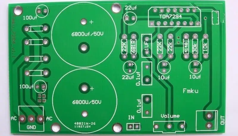
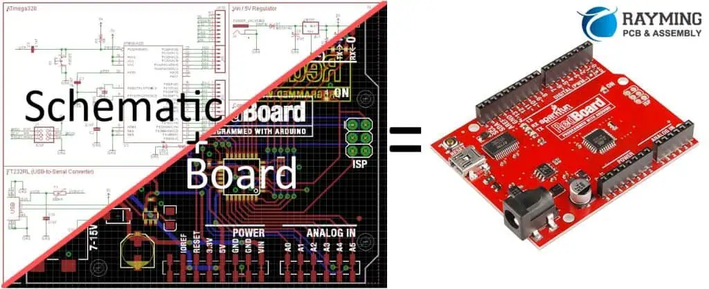
A circuit schematic is a core part of your PCB design and PCB layout. It is an aspect of a PCB design process that requires carefulness and attention. At first, you will begin with the creation of a block of diagram and then a circuit schematic. Circuit schematics are not usually designed manually. To design a circuit schematic, you will need a PCB design software.
A circuit schematic is important to engineers and designers just as a recipe is to a chef. This schematic indicates the needed components and parts and how to use them. A circuit schematic in PCB design depicts the design and layout of the printed circuit boards.

What is a Circuit Schematic?
A circuit schematic displays a view of an electronic system. In this view, components are displayed as separate blocks in a circuit with outputs and inputs. Also, these components can appear as a component symbol in a circuit diagram. A circuit schematic shows complex devices as blocks in order to get rid of the need to display passives and single transistor in the component. With this, it becomes easier to display connections between ICs, passive components, and other components.
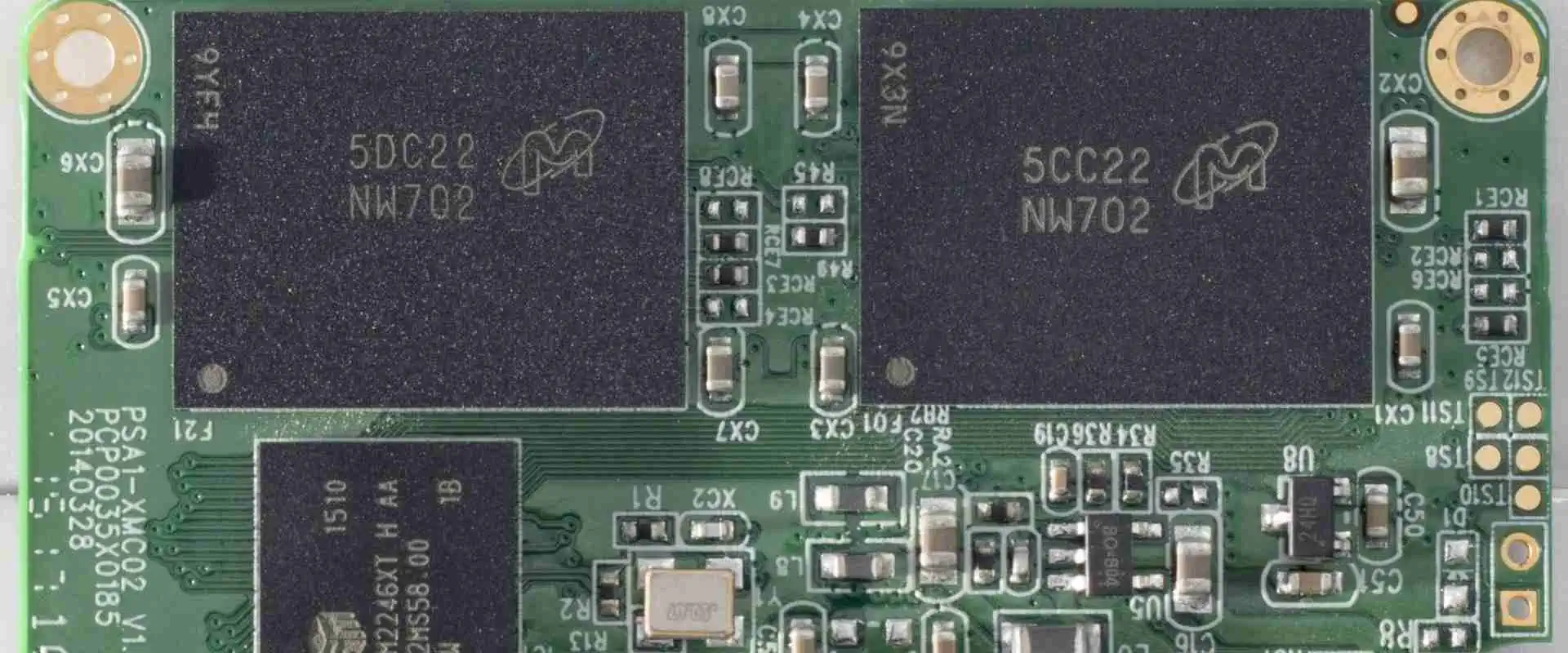
A PCB design usually starts with a circuit schematic. In a circuit schematic, symbols represent components and reveal their electrical connection. This schematic is usually created before the design layout of the PCB. PCB layout can begin when the schematic’s functionality has been verified. Also, a PCB schematic reveals the integration of various electronic components.
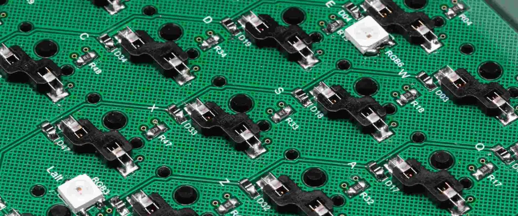
These components are both passive and active components. The circuit schematic comprises the arrangement of these components in a readable format. Also, a schematic enables viewers to know the connectivity among several components. With this, it is easy for designers to understand the arrangement of components on a circuit board. Also, a schematic provides easily readable arrangement of the electrical circuits.
A circuit schematic is useful in electrical engineering as it helps in designing a whole circuit before developing it. Also, you can use a circuit schematic to offer explanation on how electronics operate without the need to detail the software or hardware integrated in the actual electronic.
What is the Difference between a Circuit Schematic and Circuit Diagram?

As an engineer, you must have learnt about circuit diagrams at a point in time. However, there is always a mix up between circuit diagram and a circuit schematic. People usually confuse these two terms, but there is a difference between them.
A circuit diagram displays a better view of the fundamental combination of circuit elements to create an IC. It is a representation that displays the functionality and connection between electrical components. A circuit schematic will require a complex circuit diagram for an IC in a box with outputs and inputs.
A circuit schematic connects back to graphical footprints for various components and component models. On the other hand, a circuit diagram integrates the basic circuit elements to display functionality. With this, PCB layout and simulation are made easy. A circuit schematic references the separate circuit elements in a particular component.
A circuit diagram represents an electrical circuit. This diagram is integrated for circuit design, development, and maintenance of electronic and electrical equipment. A circuit diagram is also referred to as an electronic schematic or electrical diagram.
What is a Schematic Capture?
A schematic capture is just like a blueprint for the construction of a new building. This document is very fundamental for a PCB layout. It guides the designer on how to lay out a device on a printed circuit board. When you are done with your schematic capture, you can now translate the schematic in an real PCB layout.
Difference between a Circuit Schematic and Block Diagram

People often interchange a block diagram and a circuit schematic. These two documents aren’t designed to provide the same information. Your PCB design process usually begins with a block diagram. This diagram displays a function view of how the system operates. Functional view simply refers to the functions that integrate analog signals and data in the system.
Each part of the systems is named according to the function it carries out. A block diagram majorly focuses on how the system operates. Also, a block diagram is capable of making references to components while aiming on revealing the functioning of the system.
This is when the circuit schematic comes in. The circuit schematic helps in breaking each of these functions into components. You have to develop a circuit that offers the necessary functionality for every functional block. A designer might need to integrate hierarchical schematic design for complex devices having multiple block diagrams.
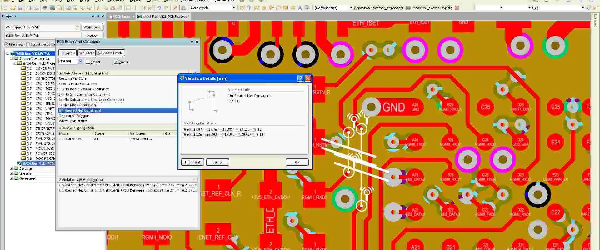
Designers need to integrate an efficient PCB design program when designing a circuit schematic. This program should come with schematic capture features. Design software programs like OrCAD, UpVerter, and Altium Designer are great options.
Six Steps to Developing Circuit Schematic online
To get their concepts from of the breadboard then to the Circuit board manufacturing facility, electronics design professionals must complete a wide range of duties. Yet making the schematic drawing ranks among the most crucial tasks they must complete.
As significant as electronic design is the schematic drawing. The schematic must be accurate, clear, and concise since it’s going to be reviewed by several other engineers as well as PCB manufacturing experts. A properly created schematic makes the design’s purpose, function, as well as goals clear. Follow the steps below to create a circuit schematic which will help others comprehend and produce your PCB:
Create the block diagrams that will show your design in detail
With block diagrams, you can introduce the electronic designs to any reader. It serves as a straightforward summary of a design architecture as well as provides the reader with a framework for comprehending what the design accomplishes. The systems plus other supporting systems of the hardware design should be summarized. Block diagrams may be created quickly. Ensure that every section of your block diagram includes a unique page number which points to the relevant section of a schematic drawing in order to aid the reader.
Mark each net
The circuit schematic drawing can be described as a tool which you and other people will are using for simulation and debugging runs in addition to being a visual representation of your electronic designs. This schematic needs to have the nets identified in order to carry out these significant tasks. Although it seems like a time-consuming activity, it will be useful later on.
Each net needs to be marked with its intended use. Even though some engineers might disagree, naming the nets can save you as well as others a ton of time.
Include as much information that’s possible in your schematic
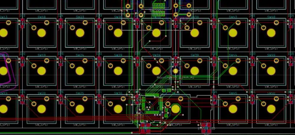
Don’t make your schematic sketch too simple. Instead, be as specific as you can. Schematics that are shortened and oversimplified are challenging to understand. A different engineer or your PCB assembly company could be unable to replicate the electronic design when they can’t follow the schematic. It’s okay if your diagram takes up several pages. The general schematic, which should include block diagrams, should flow through each page in an orderly, readable manner.
List every connector and pin
A schematic sketch has a lot of details. It has pins, connectors, components, and more. Make sure that the reader can tell the difference between a connection and a pin. Labeling the connectors and organizing the pin placement are both recommended. Keep in mind that you are an expert on your design. But, others will be using your schematic for carrying out their tasks. Make it straightforward, understandable, and simple.
Save Your Electrical Design Notes in a Record
Readers can better understand your design by using design notes. Save a copy of the notes for your records. The crucial ones should even be noted in a separate document that is attached to the schematic as well as footnotes present on it. What information is added to the schematic drawing’s notes? It should include those regarding selecting components, configuring logic tables, thinking about power supplies, and more.
The goal and meaning of the electronic design should be made abundantly evident in the schematic representation. The reader should have no trouble following it. Your design would be simpler to duplicate, understand, simulate, as well as debug if you develop a comprehensive schematic drawing.
Employ the Appropriate Tools for Schematic Design
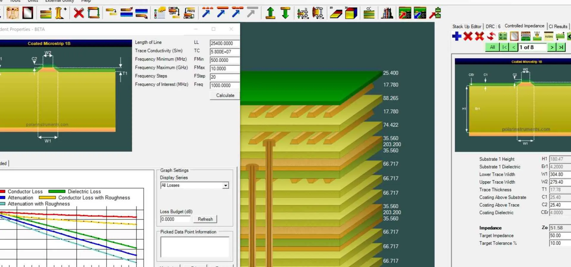
Simple electronic designs could have hand-drawn schematics. Yet, having a professionally created schematic is advantageous if you’ve got a complicated design that makes use of several elements and surface mount component. Schematics cannot always be produced via PCB design softwares. So check to see if the software for PCB design can generate a quality schematic drawing.
Best PCB Design Software for Creating Circuit Schematic Online
In the past, electrical engineers and designers use pen and paper to create a circuit schematic. However, the advancement in technology has paved a much better way to create a schematic conveniently. There are now software programs with features that help you create a good circuit schematic online. With these programs, it is faster and easier to create a schematic for your electrical circuit.
However, you need to understand that not all software design packages offer features that create a good circuit schematic online. Therefore, we have helped you to list out best software packages that offer advanced features for creating a circuit schematic.
CircuitLab
This is a good program specially developed to create a circuit schematic. With this program, you can run a simulation check to be sure if the plotting and components are correct. CircuitLab offers advanced features that enable you to easily create a circuit schematic online. However, you can’t have access to this software offline. However, it runs on popular websites like Firefox, chrome, and Edge as long as your internet connection is stable.
EasyEDA
EasyEDA is one of the most popular software packages that allow designers to have a great experience while creating a circuit schematic. With this software package, designers can easily visualize and analyze a circuit’s output. Also, this software offers a collaboration feature which helps designers to plan a circuit layout. EasyEDA allows you to improve the diagrams you created with 3D views. With this, you can visualize designs in a better way. EasyEDA is a free circuit schematic maker where you can get readily available designs.
Autodesk Eagle
This superb software program helps designers to create a circuit schematic online. It is very helpful when you have a large number of electronic components to work with. One of the advanced features of this software is its extensive variety of PCB layouts. Also, users have the opportunity to choose from several customize options such as routing, loop removal, and cornering. Furthermore, this circuit diagram maker allows you to integrate 3D elements on diagrams.
Benefits of Using Schematic Design Software
PCB design software programs offer a lot of benefits when integrated in creating a circuit schematic. Some of these benefits include lower design cost and more efficient wiring layouts.
Allows integration with other software
A circuit schematic design software allows designers to import and export data from other software. This makes designers have a stress free experience when creating a circuit schematic online.
Enables automation of several functions
Another benefit of using a circuit schematic design software is that it enables you to automate several functions like searching, list generation, cross-referencing, and the likes.
Conclusion
A PCB design usually starts with a circuit schematic. In a circuit schematic, symbols represent components and reveal their electrical connection. This schematic is usually created before the design layout of the PCB. PCB layout can begin when the schematic’s functionality has been verified. Also, a PCB schematic reveals the integration of various electronic components.
The circuit schematic plays a crucial role in the design as well as manufacturing of the circuit board. It can be said that this graphical representation lays the foundation of a PCB design. We have outlined the steps on creating a circuit schematic online and the best software for it in this article.