Why is Xilinx XC7A50T-2CSG324I FPGA needed for Next-generation applications?

Xilinx Zynq

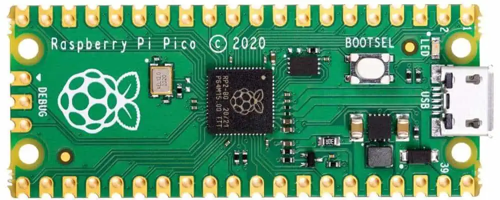
Applications are those modern applications that use technology. They necessitate rapid data processing, minimal latency, and low energy consumption. These types of applications are developed to manage colossal volumes of data while delivering real-time outcomes. Some examples of next-level applications include artificial intelligence, machine learning, 5G wireless networks, field programmable gate array, and IoT or the Internet of Things. Similarly, The Xilinx XC7A50T-2CSG324I is a cutting-edge Field-Programmable Gate Array (FPGA). It is designed to cater to the demands of the coming generation’s applications. FPGS are used in a plethora of sectors, such as aerospace, industrial, automotive, medical, and telecommunications. It’s all because of their dynamic architecture, modifiable design, and low power usage.

The following content will take you deep into the Xilinx XC7A50T-2CSG324I’s prime features. It will also explain to you how it is propelling the next-generation applications. First of all, you must have some basic information regarding Xilinx XC7A50T-2CSG324I.

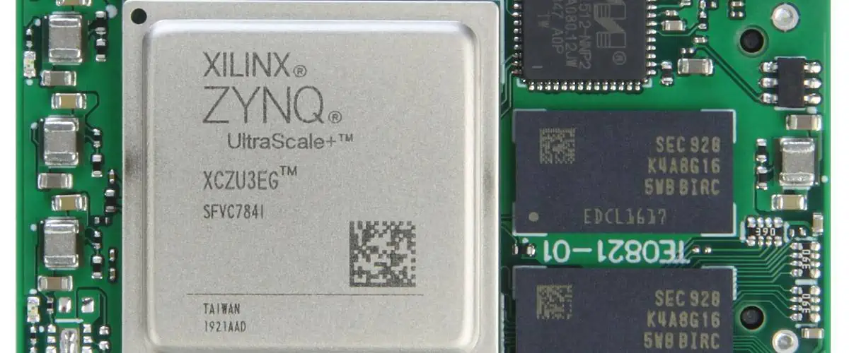
What Is the Xilinx XC7A50T-2CSG324I and Why It Is Famous for?

Xilinx Virtex-5 fpga

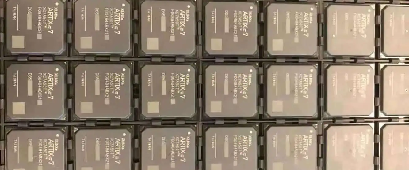
The Xilinx XC7A50T-2CSG324I belongs to the Xilinx 7 series of FPGAs, which utilize a twenty-eight-nanometer blueprint. It is an exceptional apparatus that encompasses a dual-core ARM Cortex-A9 processor coupled with a vast array of configurable logic blocks and input/output resources.

The XC7A50T-2CSG324I has a highly flexible design. That’s why it allows for a broad spectrum of customization options. You can easily customize it to match a specific application’s needs. It includes image and signal processing, control systems, and high-speed data transfer.

Reasons to tell you why Xilinx XC7A50T-2CSG324I is the need of future

1. High-Performance Architecture with Real Time Processing

ย The Xilinx XC7A50T-2CSG324I boasts a high-performance architecture incorporating a dual-core ARM Cortex-A9 processor. Its high-speed configurable logic blocks are just icing on the cake. They can deliver exceptional processing power and performance. As a result, its real-time processing capabilities make it an excellent fit for high-speed data transfer. In addition, it takes less time compared to the microcontroller. Video and image processing applications also have XC7A50T-2CSG324IPower efficiency.

2. Great Energy Efficiency

This FPGA has the best features and great applications. Despite the outstanding architecture, the Xilinx XC7A50T-2CSG324I is energy efficient. Yes, it is a great plus point. This FPGA prioritizes energy efficiency. It has refined power management capabilities. ‘s why it enables it to work at low power levels without impeding its performance. Yes, impedance is the biggest issue when it comes to power management. Micro controls find it hard to deal with impedance. This makes it the best option for low-power-consuming applications. Low power-consuming modern devices such as battery-powered devices and embedded systems have XC7A50T-2CSG324I.

3. Flexibility For Better Customization

Previously micro, microcontrollers were pre-programmed, that’s why it was hard to program them. The Xilinx XC7A50T-2CSG324I exhibits remarkable flexibility. You can easily customize it according to your needs.

 It has a range of customization options. That’s why it is easy to be programmed according to the needs of a particular application. It has a fair number of logic blocks, that’s why it is easy to program it. It also has a myriad of input or output resources. As a result, it is easy to match it with a different application. The good thing about this FPGA is greater customization. Yes, you can program it according to design and need. That’s why it is ideal for different applications in different fields. Xilinx XC7A50T-2CSG324I FPGA is the need of modern next-generation applications due to its customization. Every time when you use it on the device, then you can easily integrate it into the new application.

4. Next Level Scalable Performance

 The Xilinx XC7A50T-2CSG324I offers scalable performance. All modern next-generation devices may show varying degrees of proc. It has the ability to use power and performance. That’s why this FPGA can serve better. It has the ability to take performance to the next level. It is easy to work with different devices that provide diverse levels of performance and functionality. That’s why it is easy to integrate it with systems for automation; as a result, it shows better performance and better efficiency.

5. User-Friendly Features And Interface

The Xilinx XC7A50T-2CSG324I’s advanced capabilities do not compromise its user-friendliness. It has an array of development tools and software that simplifies the programming process. It has a user-friendly interface. Even a hobbyist can easily use it if you have a fear of not handling it properly. You can take help from the community. There are several online tutorials regarding Xilinx XC7A50T-2CSG324I FPGA. That’s why it is the need of all contemporary hi-tech applications.

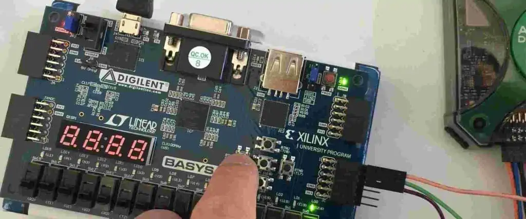
Are There Any Development Tools Available For Xilinx XC7A50T-2CSG324I?

Xilinx provides a range of development tools for all of its FPGAs. When it comes to Xilinx XC7A50T-2CSG324I, then again, there are different tools. Vivado Design Suite and the Xilinx SDK are at the top of the list. That’s why it is easy to program and reprogram this FPGA. These tools have exceptional features that are why designers andย developersย can design, simulate, and debugย Xilinx XC7A50T-2CSG324I.

How Is The Xilinx XC7A50T-2CSG324I FPGA Better As Compared To The FPGAs In Its Class?

FULL PCB MANUFACTURING Quote

Xilinx XC7A50T-2CSG324I offers a good balance of performance and low power consumption. Although all FPGs show good performance, the XC7A50T-2CSG324I FPGA has a large number of I/Os and other peripherals. That’s why it shows better customization and better performance as compared to their FPGAs. If you want to use any FPGA, then compare it carefully. However, the specific choice of FPGAs depends on the application design and need.

 Wrapping Up

The XC7A50T-2CSG324I is a formidable FPGA. It has great potential to revolutionize the next generation of applications. Its exceptional capabilities and adaptability make it a versatile tool in various industries.  The technological advancements continue to accelerate at a breakneck pace; the need for high-performance FPGAs such as the XC7A50T-2CSG324I is expected to surge. That’s why we call it the heart of next-generation applications. Its cutting-edge technology and innovation are enough to make it part of the future application. If you are searching for a powerful and more adaptable FPGA for your next project, the XC7A50T-2CSG324I is undoubtedly a worthy consideration.

Let’s Explore XC7A200T-3SBG484E’s Specifications and Features

Xilinx Artix 7

FPGAs are emerging as a popular choice among hardware designers and engineers. These programmable offer a high degree of flexibility, scalability, and customization. That’s why they are suitable for a wide range of applications. You can find them in several applications, from aerospace to consumer electronics. Now, days every other sophisticated device has FPGA to enhance its working performance.

One of the most powerful and advanced FPGAs available in the market today is the XC7A200T-3SBG484E.  This FPGA has amazing features. It is a quality FPGA by Xilinx. You all know that Xilinx is a leading company in the FPGA industry.   This company is famous for its innovative and reliable products.

What Is XC7A200T-3SBG484E?

The XC7A200T-3SBG484E is a part of Xilinx’s Artix-7 FPGA family. This family is famous for low-cost and low-power applications. Moreover,  it is based on a 28-nanometer (nm) process technology. This latest technology enables it to deliver high-performance features.  In addition, it maintains low-power consumption. As a result it is ideal for compact and battery-operated devices.

This FPGA features a programmable Logic capacity of 215,360 logic cells, which makes it suitable for a wide range of applications. As a result, it offers high-speed processing and data transfer. It also comes with several built-in features and interfaces, such as gigabit Ethernet and PCIe. Similarly, it has Gen2 and high-speed serial transceivers to enhance its capabilities.

Let’s have a look at its specifications.

Key Specifications     

Xilinx FPGA Programming

 This FPGA comes in Package: of 484-pin ball grid array       

  • This FPGA offer Speed grade -3 
  • The operating temperature range is between -40ยฐC to +100ยฐC
  • It has 215,360 logic cells. These clues are the basic building blocks of this FPGA.      
  • It has 860,160 CLB flip-flops and 430,080 CLB LUTs
  • Block RAM of 5,040 Kb is just the icing on the cake.
  • 740 DSP slices make signal processing more convenient.
  • 32 Transceiver count is an added feature        
  • 400  user Input and output pins  
  • Core voltage 0.95V to 1.05V  is for this FPGA 
  • 1.8V is auxiliary voltage for it.  
  • Gigabit Ethernet and PCIe Gen2 interfaces

Unique Architecture And Design

The XC7A200T-3SBG484E has a highly optimized architecture.  As a result, it combines several advanced technologies to deliver maximum performance.  Its efficiency is unmatchable. It features a configurable logic block. That’s why it is easy to be customized and implement various logic functions. For example, it is ideal for arithmetic functions, memory, and combinatorial circuits.

This FPGA XC7A200T-3SBG484E also includes a variety of specialized blocks. For example digital signal processing blocks and memory blocks are some special blocks.    In addition Input and output blocks are just icing on the cake. That’s why it is easy to implement even complex functions and algorithm.  It also has a flexible routing matrix. It also supports different interfaces.  As a result, it allows designers to connect different blocks and modules.   In addition, it optimizes their design for specific applications.

Advanced Debugging And Monitoring Features

  • It has up to date debugging and connectivity features that make it ideal to use.
  • Integrated Logic Analyzer allows for real-time capture and analysis of signals within the FPGA fabric. The 
  • A logic analyzer can capture signals from up to 256 probes.  It offers a maximum frequency of five hundred MHz.
  • Integrated Memory Controller supports several industry-standard memory interfaces. For example DDR3, DDR2, and QDR II+.
  • Integrated PCIe Endpoint Block: This allows for high-speed communication with external devices. It is possible through a PCIe interface    
  • JTAG Boundary Scan is helpful for testing and debugging board-level connectivity issues.  In addition, it test and program the FPGA and its functionality.   
  • Power Monitoring allows designers to monitor the power consumption of the device and optimize their designs for power efficiency.
  • These advanced debugging and monitoring properties of the XC7A200T-3SBG484E FPGA make it eminent among all other FPGAs. If you are
  • Looking for debugging and security features, then this FPGA serves better.  In addition, it allows designers to quickly identify and correct issues in their designs.

Alphanumeric Breakdown Of XC7A200T

FULL PCB MANUFACTURING Quote

At first glance, you may consider these numbers and the alphabet as ordinary numbers. But these alphabets and numbers show significance. They have some meaning. Following the breakdown of these alphabets and numeric will help you to know about this FPGA.  XC is the prefix. Mostly   Xilinx uses it to identify their FPGA products. So if any FPGA name starts with XC, then, you can understand its manufacturer. 7A indicates that the FPGA is part of Xilinx’s Artix-7 family. Xilinx has different FPGA families, and FPGAs belonging to particular families has different specifications. That’s why it is necessary to

Know about the FPGA family.  As a result, you can easily understand the basic features of this FPGA.

  • 200 represents the number of logic cells in the
  • FPGA. In this case, these logic cells are 215,360. These building blocks make FPGA and you can’t expect any FPGA without it.
  • T indicates that the FPGA is a -3 speed-grade device.  In addition, it means it can operate at a maximum speed of 1.25 GHz.
  • 3S tells about the package type of the FPGA. That is simply a 484-ball, 0.8 mm pitch, BGA. BGA stands for ball grid array.
  • BG484 is the package code that identifies the physical Package and pinout of the FPGA. So without opening the Package, you can know about the product inside.  E indicates that FPGA is RoHS compliant. It means that it doesn’t conation lead or any harmful material

Wrapping Up The Things

Nowadays, most modern applications use the  FPGA due to its unique features. That’s why an FPGA is more sophisticated than any microcontroller. So go for any one of them by keeping your needs in mind. Above all, if you find yourself confused, you can seek professional or expert help. In our opinion, XC7A200T-3SBG484E has unique architecture and debugging features. That’s why designers that prefer superior architecture can go for it.  Above all it is good XC7A200T-3SBG484E FPGA.

Understand the Difference between OSP vs. ENIG Surface Finish for PCB: Which is Better?

OSP Vs ENIG

Printed circuit boards are now more crucial than ever due to their excellent properties. Today, you cannot think of developing consumer electronics without PCBs at all. However, it is obvious that the PCBs are building blocks of futuristic electronics on all counts.

 It means these have to be faultless as well. Or else they will fail to let the electronics perform in their natural state. If you are reading this post, you must be coming from a technical PCB background. 

Assuming this, you know that PCBs have several important components that render them different features. One of them is surface finish. It is like a covering that is present between a regular PCB and all of its components.

 There are two highly important roles of surface finish for PCBs. Number one is to secure the copper components, and number two is to create enough room for soldering these components with PCBs. 

There are different types of PCB surface finish. We are going to have a look at two common types called, OSP and ENIG, in this post.ย 

OSP Finish

PCB Manufacturing with OSP Surface Finish

An OSP is a natural and fine form of surface finish used for PCBs. The OSP comes in a natural state and does not include toxins, chemicals, and artificial additives. Now, the natural form of OSP makes it important for reducing corrosiveness. 

OSP surface finish is also eco-friendly. You can even use OSP with RoHS applications. Keep in mind that OSP includes water and develops a smooth surface for the components assembly of PCBs. 

Besides, it is a budget-friendly surface finish, and many manufacturers prefer to rely on it due to its exceptional qualities. Sometimes, even using a HASL cannot yield fruitful results. However, OSP saves you from any sort of hustle because it is a great substitute for HASL for PCB surfaces.

 Now that you know well about OSP, its time to hop onto the typical process it follows through this 6-step guide:

  1. Cleaning: The process begins with cleaning the PCB’s surfaces in case oily residues, solder fragments, toxins, and corrosive chemicals are present on them.
  2. Topography enhancement: The next step is to etch this surface which will solidify the connection of PCB and OSP itself but make sure to etch the surface with an optimum pace. 
  3. Acid rinse: Now rinse the PCB with sulfuric acid after you have completed the etching step. 
  4. OSP application: Once you have rinsed the PCB with sulfuric acid, you are good to go with applying the OSP to the PCB surface.
  5. Deionization rinse: The OSP that you have just applied on PCB is ionized, which is perfect for assisting in the soldering step of PCBs. 
  6. Dry: The last step is to completely dry the OSP layer to avoid problems. 

Downsides of OSP surface finish:

  • It might not overcome dents and impressions
  • The OSP can sometimes create a negative impact on soldering
  • OSP does not promise longer shelf life as compared to other types 

Common uses for OSP include:

  • Fine pitch devices: OSP does not involve pad and ridged surfaces, which makes it perfect for utilization in fine pitch applications
  • Server boards: OSP is a reliable option to choose when it comes to server boards that work on a higher frequency
  • Surface mount technology (SMT): OSP can easily serve well for the SMT PCB components, saves time, and offer quick assembly 

Advantages & Disadvantages of OSP Finishes 

Advantages

ยท Lead-free

OSP is an organic type of surface finish. The best part about its organic nature is that it is more eco-friendly than other types of surface finish present, like HASL, which creates an adverse impact on the environment. 

ยท Cost

It is an affordable to go for. OSP does not need high-end and rare materials for processing the PCBs. Due to this, it is accessible to most PCB producers at a much lower price. 

ยท Flat PCB surface finishes.

The texture of the OSP surface is flat and smooth. It means OSP will allow fine regulation of congested and sensitive PCB components. Unlike HASL since it interferes with the performance of PCB parts. HASL interacts with residues, fragments, and air particles and also locks the solder paste within the system. 

ยท Simple process

The process of OSP application is not extensive. It only involves six steps that are easy to carry out. It means technicians can perform OSP easily and quickly without any fear of mishaps and complications. 

ยท Repairable

The OSP is a repairable surface finish. Now what does โ€œrepairableโ€ mean here? The repairable nature of OSP means if it chips off from any area, you can fix it. Also, if the finish gets damaged due to any reason or if you want to add more solder with the OSP, it is possible.ย 

FULL PCB MANUFACTURING Quote

Drawbacks

ยท Limited to RoHS compliance

If you are considering OSP, then keep in mind that it only fits well with RoHS applications. The substances like cadmium and mercury perform perfectly with OSP. Due to this reason, OSP is useless to use for external applications other than RoHS. Therefore completely relying on OSP for other applications is not recommendable. 

ยท Environmental impact

There is no doubt that OSP does not need lead. But it does use some solvents and chemical substances that are not healthy for the environment. The cleaning step of the OSP application process leaves excessive dirty water that can lead to polluting the environment through water-borne diseases as well. 

ยท Sensitive

OSP is not suitable for exposure to extremely hot temperatures for long periods of time. The OSP can completely chip off from the PCBs. It means the boards need to be re-processed, and it will be a lot of time-consuming.

ยท Short shelf life

All the surface finish types that involve water have a small shelf life. It means it will get expired and be useless after two months. Now, if you want to use OSP, then use it within two months of its accurate shelf life. You cannot leave any amount of OSP open since it can go waste due to environmental changes. 

ENIG Fnish for PCB

ENIG surface finish is much more expensive than OSP. However, manufacturers love ENIG for their PCBs despite its rarity and unaffordable nature. It is the qualities of ENIG surface finish that intrigued the producers when it came to making their PCBs flawless. 

ENIG has a duo of coverings made of gold and nickel. The role of the nickel is to secure the copper layers and to strongly join the components of PCBs together. Gold is for preventing corrosion and protects the nickel from such damage as well. 

There are some major benefits of using ENIG instead of OSP. Letโ€™s find them out below:

  • It is better for sustenance during thermal circulation
  • It is supportive of the soldering process of PCBs
  • ENIG gives an edge for wire binding over other surface finish types
  • It is also beneficial to use for high-pitched electronics just similar to OSP

Applications of ENIG:

  • ENIG serves best when you need your devices to be more tolerant instead of relying on HASL, as it does not give positive results for this purpose.

The process of ENIG is slightly similar to the OSP. However, we will still learn about it down below:

  1. The first step is cleaning which is the same as OSP cleaning
  2. The next is to etch the surface just like OSP
  3. Pre-dipping is the next step that lays the foundation for using post-dipping substances 
  4. Applying the activator is important to make sure there are no complications with the surface finish
  5. Post-dipping is for making sure the layers are well in place
  6. Applying the nickel for solidifying the connection of components
  7. Using the gold for rendering the PCB potential to fight against corrosion

Standard applications for an ENIG surface finish include:

  • Complex surface components:ย ENIG is mainly for complex PCBs, and it is the main difference that sets it apart from OSP.ย 
    • Wire bonding: The wire bonding needed by ENIG is way too less than OSP, especially for aluminum wiring networks. 
    • High-reliability applications: The PCBs used in the domains of aerospace and medical/healthcare sectors come with ENIG-based surface finish. It is because these domains work on heavy-duty equipment and complex systems that go well with ENIG surface finish. 

Advantages & Disadvantages of ENIG

Advantages

ENEPIG and ENIG
ENEPIG and ENIG

ยท Flat surfaces

ENIG is reliable for flat and smooth surfaces. It allows fine temperature regulation of PCBs and also protects them from catching fires and undergoing abrasive damage by all means possible. 

ยท Long-lasting

ENIG is a long-lasting surface finish and makes PCBs reliable in the long run as well. It promises a much higher degree of prevention against corrosion and abrasive damage. Yes, even more than OSP!!! 

It is because ENIG has gold layers that are easy to change and amend as per your needs. Once you have applied ENIG on your PCBs, it will keep solidifying with time naturally without needing any external help at all. For sensitive parts of PCBs, ENIG is suitable. 

ยท Lead-free

ENIG does not need a lead for its purpose. It means you can use it easily for your RoHs projects. Besides, it will also not create a negative impact on the environment as well. 

ยท Good for PTH

There can be no other dependable surface finish than ENIG for PTH purposes. It is sufficient to cover the entire PCB at once without making you use it again and again, which can lead to wastage. 

ยท Maintains solderability during storage

ENIG hates moisture. It means that the PCB parts are less likely to come in contact with moisture that can cause rusting. Due to this, ENIG makes sure that the PCB parts are in optimum condition all the time so that you can focus on other important things meanwhile.

Drawbacks

ยท Flammable

Now, it’s time to have a look at the dark side of ENIG. If you do not pay close attention to the layouts of your PCBs, ENIG might not like this at all. It can uncover heat-sensitive wires and cause electrical fires. The electrical short circuits can later produce fatal intoxicated emissions that are not healthy to inhale at all. 

ยท Weaker bond for components

Do you know the gold covering present in ENIG is way too thin? The thin gold layer does not give enough room for the solder to distribute completely among the pads. Now, problems can occur when the PCB parts do not adhere well to the boards due to less amount of solder. 

ยท Requires professional installation

ENIG is not something that you can manually use without seeking professional assistance. The ENIG application is only possible when you deeply know the correct method of application. 

It only happens when you are a skillful technician. So in case you are not well-familiar with the ENIG application and do it all by yourself. It can lead to wastage, thus increasing the production cost of PCBs at the same time.  

ยท Requires special materials

You cannot replace ENIG frequently. It is because the nickel and gold layers are expensive and sometimes get totally out of sight in the market. Due to this, ENIG is a questionable surface finish because it uses rare materials and equipment for the application.ย 

 The Significance Of Your PCB Surface Finish

PCB Manufacturing with Immersion Gold-ENIG Surface Finish

No PCB can work at its best if its surface is faulty. A fine PCB is one with an appropriate surface finish. The sole purpose of the finish is to protect the PCBs from harsh environmental conditions and temperature changes. Not only this, a good surface finish like ENIG and OSP will prevent corrosion of PCBs and their components as well. However, it is important to go for a suitable surface finish. 

But how do you do that? There are some factors that you can analyze in different options for surface finish. These include:

1. Solderability

Soldering is an inevitable factor to take care of when it comes to producing PCBs. The type of surface finish you are choosing can make or break the soldering as well. If a PCB surface is smooth, it will increase the strong bonds between PCB parts with the boards. Make sure your preferred surface finish provides good wire bonding. These wires include different metals, and not every type of surface finish can fit well with these metals.

2. Processing Time

Some surface finish types take a lot of time to process. For instance, HASL has by far the most extensive process of application among all surface finish types. It means the processing time of the surface finish is important to consider. Some types cannot tolerate prolonged exposures, while others can. 

3. Reliability

The surface finish needs to be reliable under harsh conditions. Otherwise, there is no point in going for expensive surface finish types. Make sure the surface finish type meets the reliability standards on all counts. Don’t waste your investment in buying an unreliable surface finish that cannot withstand complications nor ensures the protection of PCBs. 

Final Words

Now, you know well why the surface finish is an important part of the longevity of PCBs. Also, this post discusses common types that are reliable for surface finish, along with their advantages and disadvantages. You can select the appropriate surface finish based on some factors mentioned in this discussion. 

Why You Should Choose SMT Taiwan Companies

SMT Lines

As electronics designs become more complex and smaller, engineers now integrate surface mount technology. Surface mount technology has become a popular method of electronics assembly due to their sophistication and how they have contributed to the growth and development of the electronics industry.

SMT technology became highly preferred after the 1980s. Most electronic devices produced today integrates SMT. The components in mobile phones in your pocket are made through SMT. Also, electronic components in your television, cars, and more are made through SMT. The majority of modern electronic devices are manufactured with SMT.  

What is Taiwan SMT?

Taiwan SMT is a semiconductor and electronic component manufacturing company located in Taiwan, China. This company mainly engages in the production of liquid crystal display (LCD) surface mount technology in Taiwan and across the globe. SMT Taiwan specializes in the production of digital camera, notebook and television, LCD TV inverter control boards, cellular phone LCD panel control boards.

Furthermore, SMT Taiwan is known for manufacturing products such as touch panel control boards, TV SET control boards, lighting application control boards, wireless controllers, automotive dashboard panel backlight bards.

In 1990, this company was incorporated. SMT Taiwan has their headquarters in Taoyuan, Taiwan. As a well-known SMT company in Taiwan, they make use of sophisticated SMT equipment and procedures in manufacturing their electronic products. Their products are used in several applications which include consumer electronics, medical, telecommunications, and industrial control systems.

SMT Taiwan has continued to earn the trust of their customers and as such has many loyal customers across China and the world. This SMT company has a good customer base across several countries in the world. Furthermore, SMT Taiwan has been able to set the standard for surface mount technology and its integration. Taiwan SMT comprises effective SMT lines you can work with for any SMT assembly project you want to execute.

Other SMT Companies in Taiwan

SMT X RAY CHECKING

Taiwan has several SMT companies which are some of the best SMT companies in the world. These companies are known for their specialization in the production of electronic boards and products via surface mount technology. Here are a few SMT companies in Taiwan.

Hong Chi

Hong Chi SMT company in Taiwan carries out projects like surface mounting, wire bonding, chip bonding, and circuit board assembly. Although this company started as a DIP factory, it has created its own SMT factory to experience growth.  Hong Chi uses quality materials and components to produce its electronic products. It believes in offering quality SMT products and services to customers.

Furthermore, this company has maintained a good working relationship with many outstanding companies in Taiwan. They specialize in the design and manufacturing of products like telecommunication products, computer peripherals, medical equipment, and more.

Acrotec International

When it comes to efficiency and quality, Acrotec International is one of the SMT companies in Taiwan that offers such. It has built a world-class reputation in SMT and PCB production. Since its existence this SMT company has endeavored to meet the constant demands of their clients through efficient production, good customer service, and quality products. Also, Acrotec International can go through the SMT process with accuracy. Their various products can be integrated across several industries.

Albewell Electronic & Technology

Allbewell Electronic & Technology has been existing since the year 1982. As a reliable company, Allbewell works with skillful and professional engineers. It is one of the leading and highly preferred SMT companies in Taiwan. This company offers one-stop services to its customers which include PCB layout, PCB design, assembly of PCBs, and PCB packaging.

Also, this company sees to the increasing demands of its customers. Albewell Electronic & Technology makes use of skilled and knowledgeable procedures and equipment in its SMT process.

UGIC Group Corporation

UGIC Group Corporation has been in the PCBA industry for more than 20 years. It makes use of SMT all through its PCB production process. Some of its services include PCB design, PCB fabrication, and circuit board assembly. As an experienced SMT company in Taiwan, this company has a huge customer base and has been able to maintain quality throughout its production process.

Benefits of Choosing SMT Taiwan

There are so many benefits you get to enjoy from Taiwan SMT when you hire them for your SMT project.

Quality

Taiwan surface mount technology corp. integrates quality measures and procedures when manufacturing their products. Also, this company ensures all of its products undergo appropriate testing to evaluate functionality and performance. Another way SMT Taiwan guarantees quality is through their quality control process. From the point raw material sourcing to manufacturing and distribution, SMT Taiwan ensures all these processes adhere to the right standards in the industry.

A wide range of products

SMT Taiwan produces different electronic products and circuit boards. The products of this company include industrial equipment, lighting products, TVs, and more. Asides from using SMT in its production, this company ensures its products are available to various customers in different fields.

Experience

This company has an experience in SMT production. As a renowned company in Taiwan, SMT Taiwan has been operating for years. When you hire this company, you are working with an experienced SMT company. Due to its experience in this aspect of PCB production and electronic manufacturing, SMT Taiwan has been able to acquire effective skills and also develop them.

Good testing services

The testing services offered by this company are unique. Before it commences with production, it has a team that tests all products. Testing guarantees the quality of a product and this is important when you are choosing a company to work with.

Timely delivery

The importance of timely delivery is clearly understood by SMT companies in Taiwan. PCB users understand how a short lead time can affect their activities positively. This company ensures its electronic products are delivered according to the customerโ€™s specified time. SMT Taiwan is an SMT company that offers fast turnaround.  It doesnโ€™t compromise the quality of its products while offering short lead time. This is indeed an added advantage for customers who choose this company.

SMT Machines Integrated by Taiwan SMT

During the process of surface mount technology, machines are usually automated. Below are some machines used during this process.

Solder paste printing machine

The solder paste printing machine holds the circuit board in the right position and then applies solder paste on the PCB surface. This machine has a squeegee which applies the right amount of solder paste on the pads.

Pick and place machine

The pick and place machine picks up SMT components and then places them in the appropriate locations. Pick and place machines are available in three different types which are the manual pick and place machines, automatic, and semi automatic machines. The manual pick and place machine require an operator to operate while the automatic machine operates without any human intervention. It automatically picks and places the components.

Equipments for inspection and repair

When surface mount technology is ongoing, there could be errors and there is a need for you to detect as well as repair them immediately. This inspection and repair equipment helps in detecting all the boardโ€™s defects and corrects the,. PCB inspection during SMT is important because it ensures the electronic productsโ€™ efficiency and functionality. This equipment is accurate and precise and this is why it solves all issues before the manufacturing of the production and its eventual delivery

Reflow soldering machine

The reflow soldering machine turns the solder paste in to a molten state in order to form a strong bond between the circuit board and SMDs. It carries out this process without causing any damage to the delicate surface mount devices.

What are the Advantages of SMT Assembly?

FULL PCB MANUFACTURING Quote

SMT assembly is a method of assembling electronic components on bare boards. This technology provides many benefits which will be discussed below:

It integrates smaller components

Smaller components are usually integrated in SMT and they enable electronic producers to manufacture smaller electronic devices. Also, these components are more compact than through hole components. Therefore, this has helped engineers and electronic manufacturers to easily maximize space on PCBs. Also, this reduction has no negative impact on the performance of the electronic products.

Smaller footprint

The reasons behind the production of smaller electronic devices are smaller boards. Printed circuit boards are now available in smaller sizes due to SMT assembly. These smaller boards are now commonly used in modern devices.

More reliability

In the production of electronic devices, smaller components are now being used. These components are surface mount devices. They offer a high level of reliability since they are very small and they can populate a board in large amounts. Furthermore, applying solder paste on surfaces of circuit boards will help to reduce component failure risks in circuits.

Offers automation

Automation is an important aspect of SMT production. This technology utilizes a wide range of automated equipment during production. Also, automation makes PCB and electronics assembly faster and more accurate. There are several benefits of using automated equipment. Humans can make mistake and as such, manual processes canโ€™t be fully relied on.

Conclusion

SMT companies in Taiwan are some of the leading electronic companies in the world. Having reviewed some of these companies, we have been able to discuss the benefits of choosing these companies.

Types and Applications of an Audio Oscillator

Audio oscillators

Audio oscillators are widely integrated in generating waveforms in a particular frequency range between 16 Hz and 20,000 Hz. For a low-frequency oscillator, waveforms below 20Hz can only be generated.  Audio oscillators are designed to be used in producing music as tone generators.  

Also, these oscillators allow the measurement of compression and circuit gain at a given frequency. Here, we will explore audio oscillators, its types, and applications.

YouTube video

What is an Audio Oscillator?

An audio oscillator serves as measurement tools and tone generators in music production. An oscillator is designed to convert direct current (DC) to alternating current (AC), which generates an alternating waveform. Furthermore, oscillators help to produce waveforms in a given frequency. A low-frequency oscillator produces waveforms that are less than 20Hz.

There is a quick alternation of the electrical current between two states. This generates a waveform you can amplify and shape with different audio processors. Electronic oscillators are applicable in several industries like measurement, calibration tools, and equipment clocking.

Audio oscillators usually generate sound. Their circuitry quickly changes between two states. This is similar to the way a vibrating string generates a sound. The oscillating electronic circuit produces a waveform which you can amplify and integrate as a sound source.

Types of Oscillators

Taitien Oscillators

The Voltage-controlled oscillator or VCO is the most common type of oscillator used in analog synthesizers. A control voltage determines the frequency of the VCO audio oscillator. The VCO oscillator generates a different frequency based on the control voltage you feed it. When you press a key on an analog synthesizer, a certain voltage is sent to the oscillator. This produces a waveform in the pitch.

If you tune the oscillator properly, the pitch will work in line with the keyโ€™s note. Furthermore, with synthesizers, you can regulate the control voltage using various types of signals. For example, a Frequency Modulation also known as FM synthesis can be generated by including modulation to a VCO.

VCO audio oscillator comprises three parameters which include volume, frequency, and waveform.  Letโ€™s have an in-depth analysis of how these parameters related to a sound by looking at a sine wave.

A sine wave is the most important aspects of all waveforms. You can alter the shape of waveforms by adding harmonics. Square, sawtooth, sine, and triangle are the primary waveform shapes. Each of these shapes affects the tone of the sound generated. Also, sine waves usually have a smooth sound. On the other hand, sawtooth can be buzzy.

Noise is another waveform oscillators experience.  It usually comes in pink and white variety. While the frequencies of white noise are in equal proportions, pink noise reduces the effect of some of the higher frequencies.

Digital oscillators produce waveforms by integrating DSP or digital signal processing. These waveforms are digitally recreated to look like analog oscillators. There has been some development in modeling technology, however, a good number of synth  enthusiasts usually consider the sound of digital oscillators to be inferior to analog.

Types of Waveforms

Oscillators generate cyclic waveforms. These waveforms are measured in Hz i.e Hertz. There will be more cycles of the oscillator vibrates faster. Oscillators are known to generate different types of shapes. However, the most common shapes on an analog synthesizer include sawtooth, sine, triangle, and square. The waveform lineโ€™s curve determines its shape.

Square wave

A square wave includes harmonics that are seen in odd-number multiples of the basic frequency. Also, a square wave looks like a square.

Sawtooth wave

The sawtooth wave looks like a sawtooth blade. Odd and even harmonics are added to a sawtooth wave. Therefore, this causes a clear tone.

Sine wave

The most basic foundation of sound is the sine wave. Sine wave is pure since it has no additional harmonics included in the signal. A sine wave comprises the fundamental frequency.

Triangle wave

A triangle wave has a similar appearance as a sine wave. However, the only difference is that a triangle wave has straight edges that link like a triangle. Odd harmonics are usually added to triangle waves.

History of Audio Oscillator

FULL PCB MANUFACTURING Quote

Audio oscillators were not really suitable for modern applications in the late 1930s. This was because of their cost, complexity, and instability. Therefore, William Hewlett was inspired to design and develop the model 200B variable oscillator which was the first product by the Hewlett Packard company.

After Hewlett attended a seminar at Stanford University,  he was inspired to develop an efficient audio oscillator. In this seminar, Frederick E. Terman, Hewlettโ€™s professor, discussed the integration of negative feedback. This inspired Hewlett to spend time studying this topic for his thesis.

Hewlettโ€™s oscillator was different in that he used an incandescent lamp as the temperature-dependent resistor.  Furthermore, the light bulb functioned as an automatic gain control. This kept the loop gain of the oscillator very close to unity. This is important to achieve the least amount of distortion. The output could easily be controlled without distortion due to this design.

This performance wasnโ€™t only enhanced, but also made cheaper. At that time, the model 200A was sold at 54.40 dollars, which was less expensive than other oscillators in the market which were sold within $200 to $600.

The first method for producing audio signals was the Hewlett oscillator. Before the advent of the Hewlettโ€™s 200B, there was no accurate way to generate low-frequency signals.

What is HP 200A Audio Oscillator?

The HP 200A audio oscillator is a low-distortion audio oscillator specially designed for carrying out test on sound equipment. This oscillator makes use of the light-bulb stabilized negative feedback circuit. ย Over the years, HP oscillators were integrated for the production and maintenance of radios, telephones, stereos, and other audio equipment.

The HP200A audio oscillator was developed by Bill during his postgraduate research. As at that time, Bill had an innovative and practical idea of how to use a light bulb to provide solutions to the regulation pf the circuitโ€™s output without any interference. Although there were other oscillators, there were unstable and costly. Bill could simplify the circuit by using the light bulb. Also, he was able to enhance the performance of the oscillator and as well minimize the price.

Bill and Dave designed the HP 200A audio oscillator, their first product. The HP 200A oscillator was dubbed in such a way that it looked like it had been existing for a while. This oscillator was priced at 54.40 dollar. The oscillator was less expensive than the competitive equipment at the market as at that point in time.

According to Dave, the HP audio oscillator served as the foundation on which the HP company gained popularity and became one of the worldโ€™s largest producers of electronic instruments.

The Wien Bridge Oscillator

The Wien Bridge oscillator was designed for producing audio frequencies. This oscillator has more advantages. It is better than the phase shift oscillator since the produced frequency may be within the range of 1:10.

Wein Bridge oscillator produces a wide range of frequencies. It produces sine waves and is based on a bridge circuit created by Max Wien for measuring impedance. There are two capacitors and four resistors in this bridge. In most cases, the Wien Bridge oscillator helps to identify unknown values of components.

Most times, this oscillator is usually integrated in the audios.  Also, this oscillator is mainly used for testing audio. It can generate clock signals used for testing filter circuits. Another application of this oscillator is in testing of amplifiers. Wien Bridge oscillator can help to carry out distortion testing of power amplifiers.

In this oscillator, when there are lower to higher frequencies, at a certain frequency, the capacitor reactance and the resistance are equal to each other. Therefore, there has to be a maximum output voltage.

What is the 555 Audio Oscillator?

The 555 audio oscillator is used for producing stable square wave output waveforms of various duty cycles that ranges from 50% to 100 % or a fixed frequency of about 500kHz. In order to produce a 555 audio oscillator circuit, you can link the 555 timer IC in astable mode.  

This oscillator serves several purposes; therefore, it is used in many applications. You can use the 555 audio oscillators in various waveform generator circuits and applications where low output current is required. Furthermore, 555 oscillator is ideal for use in producing accurate pulse, square, and sine wave forms. It is a type of relaxation oscillator.

This oscillator can be easily built to flash a few LEDโ€™s. However, there is one simple way to develop a science project by integrating an astable 555 oscillator is Electronic Metronome. Electronic Metronome is a device that marks time in pieces of music by generating a recurring beat.

Conclusion

Oscillators are the best and easiest way to produce a particular frequency signal. The oscillationโ€™s frequency can vary. However, audio oscillators work within a frequency range. Audio oscillators are widely integrated in several applications. You will find them in TV, radios, and other devices.

Audio oscillators usually generate sound. Their circuitry quickly changes between two states. This is similar to the way a vibrating string generates a sound.

Significance of the ESD Standard For Electronic Assembly

ESD Standard

Change and development are necessary in life. Even in the electronics industry, there has been constant evolvement, innovation, and development. This industry is continually experiencing growth and development. While technology and device circuitry density are becoming more complex, electronics manufacturing depends more on out-sourcing.

Today it is more complex to minimize ESD losses. Users need a way to evaluate and make comparisons between competing brands and ESD protection strategies. The ESD means electrostatic discharge . This standard is important in the electronics assembly industry. It is crucial for electronics manufacturing, assembly, repair, or any other aspects that involve electronic circuits and components to adhere to the ESD standard.

What is the ESD Standard?

The ESD Standard was set up in order to ensure organization within concerned industries could protect their electronic products and components form ESD. ESD means electrostatic discharge. It is a great issue which could cause damage to an electronic component. If proper care isnโ€™t taken, ESD can destroy an electronic component completely.

Therefore, the ESD standard helps to ensure ESD doesnโ€™t build up in the first place. For instance, in Germany and some European countries, the standard DIN EN 61340-5-1 is important. The ESD standard guarantees consistency of ESDS items and as well as the consistency of ESD control products. This standard is a means of making comparison among ESD control products.

Furthermore, this standard minimizes conflicts that arise between ESD control products suppliers and users. It develops, integrates, audits, and approves ESD control programs. The U.S makes the integration of this standard voluntary. ย ESD regulations should be prioritized in cleanrooms.

What causes electrostatic discharge in electronics products?

ESD Protection at pcb soldering

Electrostatic discharge occurs when there is an abrupt electricity flow between two objects that are electrically charged. There are several causes of ESD. ESD can result from contact of the two objects by dielectric breakdown. ESD causes damage in electronic circuitry. Electricity flow can cause a hole to burn in an integrated circuit. The area which surrounds the hole would as well possess discernible heat damage.

Even if this occurrence didnโ€™t result in a hole, an ESD will disrupt the operation of the equipment. However, internal components will wear down over time due to the frequent occurrences. Lack of ESD protection will cause electronic components to easily break down. The rate at which electronic components break down will be faster. Therefore, this will interfere with operations and as such, minimize quality and enhance costs.

What is ANSI ESD S20 20 Standard?

Electrostatic discharge poses costly and dangerous risks to electronic products. Not only does it pose a great damage to electronics, it also causes damage in pharmaceutical, medical, and other important industries. To meet the increasing demand for sound ESD control programs, the ESD.EOS Association Inc set up a third-party certification program. The ANSI ESD S20.20. is a standard set up by EOS/ESD Association, Inc.

This standard was established through ISO9000 Certification Bodies. The ANSI ESD S20.20.offers technical and administrative provisions designed for some particular requirements or applications. Also, this standard offers a great basis for the control process and integration of the standard.

Furthermore, the ANSI/ESD S20.20 standard makes it possible to guide all aspects of building the ESD control programme. Also, it is ideal to be supported by the management for the area impacted by the ESD control process.

Who Develops the ESD Standards?

The development and integration of standards is usually a cooperative effort by individuals and organizations impacted by these standards. There are several major ESD standards development organizations.

Military standards

The U.S military is in charge of the developing certain specifications and standards that involve ESD control. However, the military agencies in the U.S are now depending on commercially developed standards. For instance, the ESD Association converted MIL-STD 1686 into a commercial standard known as the ANSI ESD S20.20.

ESD Association

For the past years, the ESD Association has taken center stage at the development of ESD standards. The ESD Association sees to the development of test methods and ESD standards. Also, the ESD Association  represents the United States on other programs.

Furthermore, there are several technical reports and standard documents in the ESD Association. These standards oversee the areas of test methodology for ESD control ย products evaluation and electrostatic sensitivity. Furthermore, the ESD Association published some advisories which contain some pices of information. The advisory documents may be altered in the future.

What is the IEC 61000 4 2?

FULL PCB MANUFACTURING Quote

The IEC 61000-4-2 standard defines ESD protection, by integrating two  testing methodologies. The contact discharge methodology discharges an ESD pulse from the ESD test gun that is in contact with the device under test. This methodology is highly preferred. The second methodology which the IEC 61000 4 2 makes room for is an air discharge. This methodology is ideal for scenarios in which it is impossible to maintain contact discharge testing.

The air discharge test involves bringing the ESD test gun close to the device under test until there is a discharge. These standards must be defined in such a way that each level is equivalent. Therefore, a Level 4 contact discharge of 8 kV is the same as an air discharge of 15 kV.

The IEC 61000 4 2 is an ESD immunity compliance standard for electronics that need to get the UL, CE Mark, and other certification. Electrostatic discharge ESD occurs everywhere. It occurs between high density electronic components in electronics products like television and mobile phones. It is impossible to predict ESD. Therefore, it is important to take some measures that prevent malfunction or damage of a device when ESD occurs.

The IEC 6100 4 2 is the most popular standard for evaluating robustness and approving commercial electronics. This standard is an effective EMC test standard needed to attain a CE marking. With IEC 6100 4 2, electronic producers can sell their products in Europe.

YouTube video

What is the Importance of ESD Protection in Electronic Products?

Like it was earlier explained, ESD can cause significant damage to electronic equipment and as such, this could lead to a catastrophic failure in the field. In the electronics manufacturing industry, minor mistakes or errors can be detrimental to the functionality of electronic components and devices. ESD damage is one of the most common causes of product losses.

Electrostatic discharge (ESD) occurs when built-up charge releases between objects, thereby, resulting in the flow of electricity between these objects. ESD of charged objects caused by humans statically charged objects can cause damage to different semiconductor parts which include CMOS IC chips, MOSFETs, and diodes.

In most cases, 60 to 90 percent of damages caused by ESD doesnโ€™t cause complete failure. However, this damage can be difficult to detect. Therefore, it is of utmost importance to minimize and regulate ESD during circuit board assembly.

ESD protection is crucial in any electronic products as it helps to prevent any damage. Any electronic component or product is vulnerable to damage due to exposure to ESD. Also, ESD protection is crucial in preventing the formation of static charge in electronic products. The main purpose of creating the ESD standards is to minimize the risk of damage to devices that are sensitive to ESD.

Furthermore, this protection is ideal for minimizing failure in electronic device and as well as enhancing the performance and reliability of delicate electronic components or products. Adhering to the ESD standards is crucial for industries that produce delicate electronic equipment. Therefore, the ESD standard is great measure to prevent and also address all ESD related problems.

Electronic companies need to adhere to all the procedures of ESD standards. Also, these standards should be integrated in the appropriate way.

How to Control ESD

There are some preventive and precautionary measures that can minimize ESD for electronic assembly. These measures include:

  • Make use of anti-static equipment and tools to prevent electrical charge conduction. Also, do not work on electronic device when there is electrical storm as this can increase the risk of ESD.
  • Circuit board rework or component repair should be carried out in an ESD safe environment.
  • Use ESD-safe tables or workstation to enable the dispersion of static electricity. Electrically conductive carbon fibers are used in manufacturing these mats. Therefore, ESD becomes inactive on the mat.
  • Wear a grounded wrist strap to minimize any risk of ESD incident. Ensure you wear this wrist strap correctly as it will protect any charge generated by the body.
  • ESD air ionizers can be used by engineers as they get rid of static charge from the air.
  • Employees may need to put on anti-static clothing to shield sensitive components and ESD shock.
  • Avoid using jewelry and some static accessories in the workstation.

Conclusion

The ESD standard for electronic assembly has helped in preventing some damages to electronic products. There are a wide range of standards set up to ensure safety and protection while using electronic products. Some of these standards are the IES 6100 4 2, ansi ESD s20 20 and the ISO 10605. Electronic manufacturers and assemblers should endeavor to adhere to these standards to ensure safety and reliability of electronic products.

What are the Features, Advantages, and Limitations of the Raspberry Pi Zero 2W

You can find different Raspberry models present in the marketplace. Raspberry continues to bring to us new models. Every one of these models has different features that ensure their uniqueness in different applications. The model released recently is the Raspberry Pi Zero 2 W.

Understanding the way this model functions is very necessary before going ahead to buy it. Furthermore, you must ensure that it works with your intended applications. Please read more so as to help you gain additional knowledge regarding the Raspberry Pi Zero 2 W.

YouTube video

Description of the Raspberry Pi Zero 2 W Model

The Raspberry Pi Zero 2 W can be described as the latest model of raspberry pi zero. It is a small and very powerful functional board. Also, it is a single-board and wireless computer that replaces the Raspberry Pi Zero W board. This board has a dimension of 65 nm by 30 mm by 5 mm. This is why it is known to be the smallest and high-performance raspberry pi board.

Back in 2015, the launching of the original Raspberry Pi Zero took place, and in 2017, the Raspberry Pi Zero W came to be. Few months after, the launching of the powerful Raspberry Pi Zero WH took place featuring the GPIO pins. While in 2021, the Raspberry Pi Zero 2 W was released. This particular model comes with similar features as Raspberry Pi3.

Features of the Raspberry Pi Zero 2 W include one mini HDMI port, one micro USB data port, and one micro USB power input. It can be viewed as a custom built system-in-package. In addition, this model is useful in different IoT projects, as well as smart home applications. Due to the small form factor present and its great power, the Zero 2 W model serves as a reliable computer for all your projects.

Furthermore, the Raspberry Pi features different high quality, as well as low cost adapters and cables. This allows users to enjoy their work. Also, Raspberry Pi Zero 2 W includes a Micro USB, which serves as its power source. This board comes with a great benefit of being compatible with the different Raspberry pi models. Even with its small size, it boasts powerful and great features.

With this board, it becomes easy for users to build different Raspberry Pi Projects.

What are the Hardware Components of Raspberry Pi Zero 2W

Raspberry Pi 3B
Raspberry Pi 3B

There is a need to familiarize yourself with the different components of the Raspberry Pi Zero 2W model.

RP3A0 SiP

This RP3A0 SiP is upgraded. It features a 64-bit quad-core Arm Cortex-A53 Central Processing Unit. Known as a very significant component of the hardware, the SiP is made up of Broadcom BCM2710A1 die with a 512 MB LPDDR2 SDRAM. This component is what makes the Raspberry Pi Zero 2W have additional single-threaded performance in contrast to the initial single-core Raspberry Pi.

GPIO

Raspberry Pi Zero 2W features 2 by 20 GPIO Pin sets. These pins offer excellent functionality such as digital Input and Output, SPI, PWM, and more. You might be required to solder the headers onto the GPIO headers if there is a need to make use of it.

Mini HDMI

The other models have an HDMI connector. However, this model is different. This is because it features a mini connector, which conserves space. The mini converter is very important when connecting your Raspberry Pi Zero 2W to your television.

MicroSD Card Slot

This is another excellent interface of Raspberry Pi Zero 2W. It provides support to data storage having a maximum of 32GB cards.

Wireless module IC

The Raspberry Pi Zero 2 W has on-board connectivity of both Bluetooth and WiFi. Its bluetooth is the 4.2 version, and it supports BLE.

Micro USB port

There is a micro USB port present on the left hand side which aids data communications and transmission of data. Using the USB OTG cables, connect these devices.

Camera serial interface connectors

This indicates the interface found between the processor of the RPI and the camera. You may utilize the 15-pin ribbon cables for connecting the module of the Pi camera onto the camera connector.

Best Project Ideas for Raspberry Pi Zero 2W

Here are great project ideas for Raspberry Pi Zero 2W.

Build a game station

Although the Raspberry Pi Zero 2W is a small size computer you can carry about, you can use it to build a game station you can carry in your pocket. The Nintendo 64 which is popularly used for building game stations features 4M of RAM. Raspberry Pi Zero 2W features 512M of RAM, a perfect feature for retro-gaming.

You can use the Raspberry Pi Zero 2W as a game console by simply plugging it on a TV. There are limited ports on this Raspberry Pi model. With a USB adapter and an HDMI adapter, you can easily include one game controller. However, you won’t have any port left. Developing a game station isnโ€™t a difficult thing to do. Applications like Recalbox and Retropie can be complicated to install.

Design cheap security cameras

This is one of the projects you can get done with the Raspberry Pi Zero 2W. Most security cameras are usually pricey. Also, users need to subscribe to make use of these cameras appropriately. However, most people donโ€™t know they can easily build their own cameras without having to spend too much. If you have got a basic camera module and the Raspberry Pi Zero 2W, you can build your security camera.

Since the Raspberry Pi Zero 2W is small in size, you can easily hide it discreetly. This choice is perfect for building the security camera.

Building of robots or drones

When you are building drones as well as robots, weight and size could become a major problem. Furthermore, another important thing to consider is power drain. For applications like this, the Raspberry Pi Zero 2W serves as a reliable option.

This microcomputer has a small size, is lightweight, and usually consumes lesser power. This option is much better when compared to Raspberry Pi 3B. In addition, Raspberry Pi Zero 2W allows space saving. It has a weight of 11g as well as offer high performance. Moreover, if a header is attached, it will have additional weight.

Hosts the file server

For home servers, you may utilize Raspberry Pi Zero 2W. Also, you will be able to host file servers using different options. One of these options is starting with the small distribution as well as install the Samba services. Moreover if you donโ€™t know much about text editors and command lines, there are easier alternatives.

You can try using NextCloud if your files arenโ€™t many. NextCloud is a backup solution since it instantly sends any file created on your computer to the server.

Block ads on your network

One of the project ideas recommended for Raspberry Pi beginners is the installation of an ad-blocker. You can use a Raspberry Pi Zero 2W to block ads on your network.

Ideal for music player or media center

This is another great project idea for your Raspberry Pi Zero 2W. If you have no smart TV in your home, simply install an app on your Pi model to make a good media center. The Raspberry Pi Zero 2W is a powerful and discreet minicomputer you can easily attach behind your TV.

Build binary clock

With the Raspberry Pi Zero 2W, you can build a binary clock. A binary clock uses binary to tell time. Children can easily familiarize themselves with numbers as they learn to tell the time. With the use of binary clocks, your numerical skills can be sharpened. In order to carry out your project effectively, you will require a Raspberry Pi Zero 2W and a Unicorn pHAT.

Understanding Broadcom BCM2710A1 SoC (BCM2710)

FULL PCB MANUFACTURING Quote

This forms an important component of Raspberry Pi Zero 2 W.

As an SoC, it makes use of different computer parts and components that work individually in the larger computers. Take for example, desktop computers may feature southbridge chips, separate processors, as well as graphics cards. All these are combined inside a chip.

The BCM2710A1 is made up of so many parts. Below are its major parts.

  • USB 2.0 PHY
  • GPIO Interface supports SPI, I2C, UART, GPIO, PWM)
  • 1 Giga Hertz quad-core, 64-bit ARM Cortex-A53 Central Processing Unit
  • VideoCore IV GPU
  • MIPI CSI-2 Camera Serial Interface
  • MIPI Display Serial Interface is not exposed on the Pi Zero W2!

Furthermore, it utilizes the 40nm silicon technology node. This node consumes more power than a 28nm node. Also, it offers less performance when it is in a similar power envelope.

Advantages of Raspberry Pi Zero 2 W

The Raspberry Pi Zero 2 W has more benefits when compared to some Raspberry Pi Zero.

Space saving

Raspberry Pi Zero 2 W is a very small board with less weight. This minicomputer is ideal for applications where space and weight is an issue. Because of its small size, it could be utilized discreetly in some projects.

Great power efficiency

Although the computing power of Raspberry Pi Zero 2 W is similar to that of a standard Pi 3B, Raspberry Pi Zero 2 W consumes less power. When this board was tested, it was very efficient. It has a fairer performance per watt than other Pi platform. Its idle current is lower than Raspberry Pi 3B and a bit higher than the Zero W. The board serves as a reliable option whenever you need to make use of less power as well as optimize the life of your batteries.

Cost

This is a board with low cost that provides great performance. Because it is not pricey, it is budget friendly. Even with the price, it still delivers great functionality and performance compared to the remaining models

Other benefits include the following

Wireless LAN and bluetooth connectivity are possible with the connectivity ports. This is why they work for different IoT projects as well as smart home applications

It has a small board and it user-friendly.

What are the Cons of the Raspberry Pi zero 2 W

Raspberry Pi zero 2W provides great benefits to users. However, it also comes with some cons, which will be highlighted below. Let us consider them.

  • Absence of Ethernet
  • One HDMI output, which wonโ€™t work for some applications
  • Display port is absent
  • You need to solder its header onto the Raspberry Pi Zero 2 W
  • Limited RAM
  • The camera does not have an adapter cable
  • Analog audio output is absent
  • 4K HDMI output is not included
  • The micro USB port and USB devices are too close

Related Questions

What is the best operating system for the Raspberry Pi Zero 2W?

Different operating systems can work for the Raspberry Pi. Moreover, the Raspberry Pi Zero 2W stands out and needs lightweight options such as DietPi and the Raspberry Pi OS Lite. Also, these are ideal options for any device with low specification. Apart from the above options, other operating systems that are lightweight are available for the Raspberry Pi Zero 2 W.

What are the ways of programming the Raspberry Pi Zero 2W?

This is a reliable and useful board which explains how you can program. The board provides support to the different languages for programming. To utilize this board, you will need an integrated development environment.

What areas are the Raspberry Pi Zero 2W Applicable?

Raspberry Pi Zero 2W can be incorporated as the desktop computer. This is great for use in all embedded applications. In addition, you can use it in building the robots, IoT wall devices, and more.

Conclusion

Although the Raspberry Pi Zero 2W comes with an extremely small size it provides strong and powerful features. The board ensures the easy building of different Raspberry Pi projects. Also, it is a low-cost single board computer that has a small size and works with different embedded applications and IoT projects.

What are the Color Bands and Applications of a 4.7 K Resistor?

SMD Resistor

You must be wondering what the colorful stripes found on the resistor really means. Or you really wish to know what functions the 4.7K resistors serve in electronics. Here we are to explain the ins and the outs of the 4k7 resistors. These include their applications and basic properties.

What Does a 4.7 K Resistor?

The 4.7 k resistor can be described as any electronic component that has a resistance of 4700 ohms or 4.7 kilo-ohms. This โ€œkโ€ is seen in 4k7 means kilo which indicates 1000. A resistorโ€™s resistance can be measured in ohms which is an electrical resistance unit. Resistors are useful in limiting the electric current flow in circuits and are usually utilized in different electronic devices.

You can easily recognize the 4.7k resistor due to its unique pattern of violet, yellow, red, and violet color bands. Furthermore, the band versions 5 and 6 comes with a pattern of violet, yellow, brown, black, followed by its temperature coefficient band and tolerance band on the band version 6.

There is one difficulty with the resistance 4.7 k ohm resistor. This is happening because you can easily confuse it with the 470 ohm resistor. Therefore take note of this and verify mak8ng use of the multimeter or color codes where necessary.

Color Bands of the 4.7 k Ohm Resistor

Resistor Wattage

Every band found on 4.7 kilo ohm resistors comes with a unique purpose. Regardless of the number of bands present in them, all the color-coded resistors have a minimum of two digit bands. One is a multiplier band, while the other is tolerance. This structure forms the four-band resistor color codes; the five as well as six band resistors usually add to the basic structure.

In four band resistors, the initial three digits will give the nominal value of the resistor. While the fourth band will give the resistorโ€™s tolerance. Although the resistor comes with the nominal value of 4.7k ohm, its actual resistance would vary a little bit below or above its nominal value. This tolerance reveals to us the expected range. Resistors of higher quality features improved tolerance over the ones with lower quality.

In the five band resistors, the initial four bands will reveal the resistorโ€™s nominal value. Take note that the extra band of the resistor helps in adding a specific digit to its nominal value. Consider this as an additional digit which has been added into the front, with other bands that retains similar functions as the four band resistor. Also, the final band, which is the 5thย band, identifies tolerance.

The six band resistor helps in adding a new color band at the resistorโ€™s end, which reveals the coefficient of the temperature. This indicates the resistorโ€™s sensitivity to changes in temperature. All resistors come with its own tolerance value. This means the value may not be 4.7 ohms exactly. Resistors with higher quality feature tighter tolerances.

4 Band Vs. 5 Band 4.7 k Ohm Resistor

According to our explanation, four band resistors feature two bands for the value. The first value is the tolerance while the second value is for the multiplier. Five band resistors feature three different bands for the value in which one is for the tolerance and one is for the multiplier.

The process of analyzing the five band resistor is similar to the four band resistor. Therefore, you have to look for any gap between the fourth band and the fifth bands. However, the last band in the four band resistors reveals the tolerance. You can then use the first four bands to get the resistance value.

There should be an order of violet (7), brown (x10), yellow (4), gold or silver (+-5% or 10%).

What is Resistance Tolerance of 4.7K Resistor?

The tolerance of a resistor indicates the resistance value of a resistor can feature. Therefore, the tolerance of a resistance 4.7 K ohm resistor depends on the specific series and the manufacturer of the resistor. 4.7 K ohm resistors have common tolerances which are 10%, 5%, and 1%.

  • For a 4.7K resistor with a 10% tolerance, the actual resistance ranges from 4.23k ohms to 5.17k ohms
  • For a 4.7K resistor with a 5% tolerance, the actual resistance ranges from 4.46k ohms to 4.935K ohms
  • For a 4.7K resistor with 1% tolerance, the actual resistance ranges from 4.653 ohms to 4.747K ohms

Common Applications of 4.7K Ohm Resistors

FULL PCB MANUFACTURING Quote

The 4.7K Ohm resistor is widely used in different applications. This resistor serves a lot of purpose.

Voltage dividers

4.7K ohm resistors is widely integrated in voltage dividers. These resistors produce a particular level of voltage. Also, there are two resistors on series in a voltage divider and the output voltage is very proportional to the two resistor values. Due to the tolerance level and availability of 4.7 Kilo ohm resistors, they are ideal for use in voltage dividers.

Current limiting

Also, you can use 4.7K ohm resistors to limit current. For instance, these resistors can help to restrict the flow of current via an LED. They can as well prevent the occurrence of overvoltage in a microcontroller input.

Pull-up or pull-down resistors

These resistors also serve as pull-down or pull-up resistors in digital circuits in order to ensure the maintenance of the voltage level of a signal. This is possible even in cases where you canโ€™t actively drive the signal. Therefore, 4.7K ohm resistors can prevent floating in input signals which is caused by an unexpected behavior.

Oscillator circuits

Another use case of a 4.7K ohm resistor is in oscillator circuits. This resistor helps to set the frequency of an oscillator. Also, you can use this resistor with other components like transistors and capacitors to produce a particular frequency signal.

Analogue Signal conditioning

4.7k ohm resistors serve some purposes in analogue circuits. These resistors are suitable for signal conditioning circuits as they help to adjust offset or gain of an input signal.

Conclusion

You can easily learn the color code of the 4.7 kilo ohm resistors for all resistor types. This distinctive pattern of violet and yellow band makes you spot them easily. Moreover, you may confuse them with the 470 ohm resistor that features violet and yellow bands. Therefore, it is very necessary that you verify making use of a multimeter or color code if possible.

Everything You Need to Know About CTBGA (Thin Chip Array Ball Grid Array)

BGA Chip

These days, almost all electronic devices, gadgets, and equipment are exclusively using compact, mini-size PCBs along with small variations. These PCBs incorporate various mini-size SMT components all around the surface of a PCB. Moreover, the BGA technology utilizes an under-side package of IC or pin-outs for connection rather than using the corners of an IC package.

Thus produced an HDI Printed Circuit Board, small size and lightweight dimensions product. The HD interconnects arrange in an array pattern directly under the package, which forms the pin grid. This enables the IC of a BGA to take less area over the surface of a PCB, enhances the performance, and gives more functional features in a PCB.

CTBGA stands for Thin Chip Array BGA. It refers to a type of IC package which is used in many consumer electronic devices. These devices include smartphones, tablets, and portable and wearable miniature devices. This article gives you a detailed insight into the advantages and features of CTBGA, along with its usage and applications.

CTBGA serves as an IC package that helps in making portable consumer devices lightweight and compact. It works similarly to a typical BGA package but has the size of the package and thinner chips. The package of CTBGA generally consists of copper traces, ceramic material, and a solder balls layer over the bottom of a package.

YouTube video

Benefits Of CTBGA (Thin Chip Array Ball Grid Array)ย 

BGA offers various significant benefits which enable it as a popular choice in the electronic industry. Some of those advantages include:

ยท High Density

Today, various consumer electronic devices require tiny packages with various pins. Because of this feature, engineers invented surface-mount Dual-in-line packages and Pin Grid Arrays that give track lower density. However, manufacturers of PCBs face many challenges. Pin bridging is among them. BGA, however, allows us to overcome this problem as the BGA solder balls provide the appropriate soldering needed for placing the package. Therefore, they place solder balls close to each other. This provides strength to the interconnects and minimizes the PCB footprint. BGA components create high-density interconnections which use the surface of a PCB effectively.

ยท Reliable Construction

The pins of the PGA package have a fragile and thin structure. Thus, resulting in the bending and damaging of these pins. Whereas, this is not the case with the package of BGA. In the BGA package, the solder balls are incorporated over the solder pads, which enables the network to be more reliable.

ยท Excellent Performance At High Speeds

In the BGA package, all the soldering balls are placed close to one another, which creates a close connection between components, minimizes signal distortion, and strengthens the interconnections during high-speed tasks. This shows that the network provides greater electrical conduction over high speed.

ยท Less Component Damage

Unlike PGA, the heating process melts BGA solder balls which enables them to connect with the Print circuit board. This, however, aids in minimizing the risk of component breakdown or damage.

ยท Reduce Overheating

The packages of BGA contain various thermal networks that dissipate the heat from the ICs. Thus, this effectively minimizes the risk of overheating.

Cons Of CTBGA (Thin Chip Array Ball Grid Array) 

chips-bga

BGA also comes with drawbacks, like all other electronic devices. However, the drawbacks include:

ยท Difficult To Inspect

BGA is basically a tiny material piece that allows the manufacturer to place the die of an IC over it. Because of the tiny size of BGAs, the inspection of soldering joints becomes difficult through visual inspection. However, X-ray machines and advanced microscopes may help in solving this problem.

ยท Prone To Stress

Circuit boards give flexural stress, which further affects BGA. Though, this stress causes reliability issues.

ยท Excessively Expensive

The soldering process of BGA packages requires highly expensive equipment. This, however, makes the BGA packages more expensive. Furthermore, manual soldering is used in packaging but in extremely lesser numbers.

All the above-mentioned advantages and features add up in the usage and application of BGAs. Thus, increasing the demand for Ball Grid Array packages. Though BGA devices use advanced types of technologies, they are skeptical of failures. Therefore, inspection of every joint on the board minimizes the process of rework. If you are thinking of incorporating BGA into your device. Then choose trustworthy, reliable, and industry-leading manufacturers. Various companies offer a vast range of customizable BGA packages.

Applications of CTBGA (Thin Chip Array Ball Grid Array) 

Various consumer electronic devices use CTBGA technology. These consumer devices include smartphones, wearable devices, and tablets. Some common usage and applications of CTBGA technology include:

ยท Mobile Devices

Because of the higher pin count and small size of CTBGA, manufacturers tend to use them in devices like tablets and smartphones. Moreover, applications like memory, processing, and connectivity also employ this technology.

ยท Wearable Devices

Wearable devices like fitness trackers and smartwatches use a wide range of CT BGA packages because of their low consumption of power and compact size.

ยท Consumer Electronics

Consumer Electronics like digital cameras, gaming consoles, and MP3 use CTBGA packages in them. This happens because of their cost-effectiveness and higher pin count.

ยท Automotive Electronics

Automotive electronics like infotainment systems and engine control systems also employ CTBGA advanced packages. This, however, happens because of their high thermal conduction and high-reliability features.

ยท Medical Devices

Because of the higher pin count and small size, many manufacturers use CTBGA in medical devices. However, these devices include diagnostic equipment and portable medical devices.

Conclusion

CTBGA stands for Thin Chip Array BGA acts as an advanced IC packaging. It is widely used in consumer electronic devices, which include tablets, smartphones, and mini-portable devices. Additionally, it offers various benefits and features. 

These features include high thermal conduction, higher pin count, high reliability, small size, and low cost of manufacturing. Generally, The advanced CTBGA packaging is commonly utilized in wearable devices, medical devices, automotive electronics, and consumer electronics. CTBGA plays a vital role in enhancing the demand for lightweight, high-performance, and compact devices.

Why is the Zenit PCB Tool Great for Professionals and DIYers?

Cheap PCB Manufacturer

Zenit PCB could be a very great tool for DIYers and professional designers of electronic circuits who wish to conduct a test on their designs before animating it physically. It is a PCB design tool that is Windows compatible and allows designs up to a thousand pins.

What is ZenitPCB Suite Composed of?

Zenit PCB Suite was designed for those that wish to make PCBs as a hobby or for academics and students from high schools or universities who wish to create their personal printed circuit boards with an expert approach. Particularly, this is achieved without paying for any expenses like licenses.

In addition, the full ZenitPCB suite is made up of many tools. Its layout tool allows you to design the major layout of your printed circuit boards by utilizing different components. The Zenit Capture Schematic tool is also available. This allows the user to select the circuitโ€™s components and then create a unique netlist. Also, you can find the ZenitPCB tools in a specific library called the ZenitPCB parts. This software also has the ability to read the Gerber files using its tool called the PCB GerberView.

What Does Zenit PCB Layout Mean?

Zenit PCB Layout can be described as a great tool for creating a professional PCB. This tool is a CAD program that is easy and flexible to use. It allows users to achieve their dream projects within a short period. In addition, it is fully freeware for semi-professional or personal use, which are limited to about 800 pins. It forms a borderline between professional and hobby jobs.

Using the ZenitPCB Layout, you can create your project right from the layout or its schematic capture. This is a great software for PCB layout designs for creating top-notch printed circuit boards. ย The first step here is to import the netlist (this is a ASCII file that contains the electrical information) from several schematic captures (Eagle, Protel, Pads, Orcadโ€ฆ), with the components as well as their electrical connections.

For the second case, you will be able to realize the project from your layout editor directly, import the components out from its library as well as directly connect all the pins with its cursor. Therefore, it is possible for users to create boards without having to import the netlist from the Schematic Capture. The ZenitPCB Layout has the requirements for achieving a reliable printed circuit board, makes use of the general or individual project, via the net class. You can find some of the features of a PCB here.

Now, to have better control of your project, you will be able to review the created Gerber via the Zenit PCB Gerber View.

What are the Benefits of the Zenit PCB Layout?

Zenit PCBโ€™s user interface is compact, despite its numerous application quick keys and buttons. Also, it has the major workspace at the center. On its top area, and underneath the menu bar, you will find many quick-access keys which allows users to add new circuit parts, print, save files, search, etc. Its left panel is made up of some project-related information which includes parts library, available projects, as well as available netlists.

On your workspaceโ€™s right hand side you will find shortcuts for several operations, such as drawing a circle, square, or a line in your schematic, addition of text, etc. This workspace also allows the simple drag-and-drop function; therefore it is easy to handle the tool. Zenit PCB layout is a great tool and a complete freeware for semi-professional or personal use.

What is New in Zenit PCB?

Zenit PCBโ€™s latest version comes with many improvements having all its issues fixed within all tools. Furthermore, there are new functionalities introduced. Among the significant upgrades includes the inclusion of 200 extra pins. This allows the users to utilize 1000 pins rather than the 800 pins present in the initial version.

For the ZenitCapture Schematic Tool, there are features such as auto change of the parts values, auto renaming of the net wires, the locking of all open projects, placed parts listing, alternate text printing, as well as black printing.

Furthermore, this software allows 1300 symbols. Some of the newly added features to the Gerber View of Zenit PCB include the hiding of the layers during the view, the mirror view, print preview, printing holes and printing in black.

How to Use Zenit PCB

FULL PCB MANUFACTURING Quote

To begin your new project, click on file, which is found on the menu bar and then click on New. This opens a workspace on ZenitCaptureโ€™s Schematic tool. This workspace can be described as a sheet having black and green borders that gives the location where the elements will be placed. You can then choose the components and create the circuit schematic.

First of all, click that desired element and also click the workspace so as to position it. Once the first component is added, youโ€™ll notice a positive (+) sign appear beside the Parts option which is situated on the left panel. This option can be expanded to check all the added elements. You can connect the elements by connecting a componentโ€™s connection point to the other by dragging your mouse. Once you are done preparing the schematic, you will have to pack iy inside a netlist.

Next, open your new project using the Zenit PCB Layout tool and then select the dimensions and size of the PCB you desire. You can achieve this by clicking on Place which is found on the toolโ€™s top menu and then select Board Wizard. Then, set up the components on your layout board. Next, click on File and under Import, select Netlist.

To view the Gerber files, click on the GerberView button of the ZenitPCB and select the file. This program will be able to open the NCDrill and Gerber files as well as offer visualization with respect to the ASCII format.

Conclusion

Zenit PCB is a reliable tool for all practical circuit designs. You can explore all the available options to help you discover the possibilities that the software can offer you. Zenit PCB Suite was designed for those that wish to make PCBs as a hobby or for academics and students from high schools or universities who wish to create their personal printed circuit boards with an expert approach.