Top 12 Hex Inverter ICs – All you should know

Hex Inverter IC

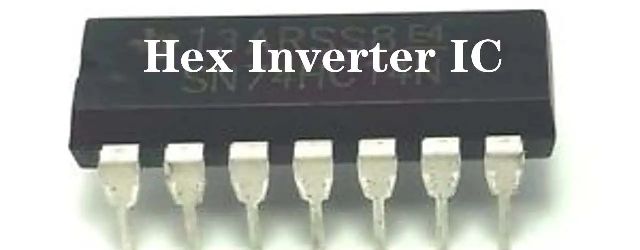
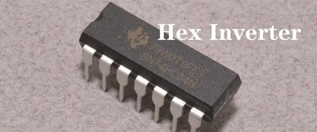
Hex Inverter is a type of Integrated circuit. The Hex in the name represents Hexa which means six. It comes with various benefits and features. These ICs are mainly used as amplifiers for analog converters among the logic series, shift levels, and added delay.  

However, you may still be concerned about why they act as an essential component in many devices and how it functions. This article gives you a detailed insight into the features, functionality, working principles, application, and types of Hex Inverter Integrated Circuits. 

Functions of Hex Inverter

Letโ€™s look into some types of hex drivers along with their functions and roles. Hex IC-4069 contains hex means six in total circuits. This type of CMOS hex IC inverter can be used in applications, especially which does not require features of medium power source TTL drives and logic-level converters.

Hex IC-7414 contains inputs of LSSTL or Schmitt trigger. Eventually, the input of Schmitt triggers converts the slow-paced signals into efficient output signals. 

The IC-7407 acts as a hex buffer that contains collector outputs. This hex buffer consists of three-phase internal circuits which create noise immunity and stable output. 

The IC-7405 consists of an open collector and output of high voltage. This simply means that it gives output with a higher voltage.

The IC-7404 also acts as a buffer. It contains a 14-dip variation integrated circuit. This makes it capable of performing six inverter insertion actions.

Applications Of Hex Inverter ICs

Hex Inverter
Hex Inverter

ยท Digital Logic Gates

Hex inverter integrated circuits serve as foundation components in digital logic gates. As it takes the input values and gives back the output value. This implies that if the input is of high logic, it returns the value of output in low logic. However, if you connect various hex inverter integrated circuits together, it generates even more complex and hard logic gates which include XOR, NOR, and NAND gates.

ยท Oscillators

Hex inverter integrated circuits are also utilized in oscillators. It helps in generating square waves, sine waves, and clock signals. The circuit of the oscillator contains a feedback loop. This loop includes a capacitor and a resistor. The capacitor starts charging and discharging over the power supply over the determined rate by the capacitor and resistor values. However, this creates a frequency waveform that serves as a sine wave or clock signal.

ยท Data Transmission

Hex inverter integrated circuits can also be utilized in circuits of data transmission which convert the digital signals from one level of voltage to the other. For instance, in serial communication of RS-232, the range of voltage of transmitted signals can vary between -12 volts to +12 volts. Therefore, many computers and microcontrollers use 5 volts and 0 volts logic levels. The hex inverter integrated circuits make it possible to convert those RS-232 level signals to levels of TTL.

ยท Signal Conditioning

The hex inverter Integrated can also feature in signal conditioning PCBs to convert the signals from analog to digital form. For instance, the hex inverter integrated circuit, along with the comparator, helps in converting the analog signal form to a digital form. The comparator gives an output value that goes into a hex inverter integrated circuit. There, it inverts the form of signals and creates a digital signal output.

ยท Power Management

The Hex inverter Integrated Circuits are also used in the management of the circuitโ€™s power, which controls the voltage supply to all other electronic components. For instance, hex inverter integrated circuits make it possible to set up the output voltage level. Moreover, it also helps in generating feedback signals. These signals further help in adjusting the output voltage of the regulator.

Hex Inverter IC 74HCT04

The IC-74HCT04 inverter consists of six self-maintaining inverters with pull and push outputs. Its pins have lower-power Schottky which enhances the speed of the IC. Moreover, it also owns a special protection network of diodes that protects the input pins from higher input Vcc. The diodes simply activate the current limiting resistors, which automatically protect the input pins.

Features of Hex Inverter Ics

The IC-74HCT04 offers various features. It is lead-free and ROHS compliant and found in packages like TSSOP-14 and SO-14. Moreover, it possesses a voltage range of 5.5 volts to 4.5 volts, along with a constant current output value of +25mA. It offers 2 volts of max value of higher input voltage and 0.8 volts of minimum value of low input voltage. Along with this, it has a 29 ns propagation delay and offers input of Schmitt trigger.

How To Use 74HCT04?

As this IC has NOT gates, t shows that it has specific output and input terminal or pins. Therefore, make sure to connect pin 16 of the IC to the power source. Then connect pin 8 with the ground. And it starts working.

ยท Propagation Delay of 74HCT04 Inverter Circuit 

The IC-74HCT04 acts in the form of a wave buffer or oscillator. However, this may require some factors to consider, like propagation delay or switching time. It refers to the period in which an output pin switches the type of input signals into another form. The propagation delay of this module is 29ns. This makes it ideal for several devices, which include buffering generators, clock signal generators, and a generator of square waves.

Hex Inverter IC 4049 IC

The Hex inverter 4049 Integrated circuit also acts as an inverter buffer with six or hex NOT gates. It is widely used in the Converter of CMOS TTL. Moreover, it is also used in various devices that have DTL converters. Additionally, it does not only function in TTL but also in DTL.

Features of Hex Inverter IC 4049 IC

The IC-4049 uses a voltage multiplier PCB and creates the max input value of the voltage supply. Moreover, it acts as a logic function of a Hex inverter buffer. It possesses various packages, which include PDIP, SO, TSSOP, and SOIC. Additionally, the max sink current of the module can rise to 2 TTL loads. It also provides a 22.5pf maximum value of input capacitance, 50mA max supply current, and an equilibrium temperature range of -40 to +85 degree Celsius.

How To Use Hex Inverter IC 4049 IC?

FULL PCB MANUFACTURING Quote

IC-4049 serves as a central component in the double voltage circuit of 12-24 volts. Moreover, IC-4049 works in a similar way as a rectifier circuit. Nevertheless, a double voltage circuit does not only convert Direct Current to Alternating current but also configures the voltage of Direct Current. Therefore, these circuits become useful for devices that are concerned with high Direct current voltages.

Applications of Hex Inverter IC 4049 IC

IC-4049 is used in various types of applications and devices. Some of them include O/P reversing, Source drivers, CMOS hex converter, voltage multiplier PCB, and CMOS converter to TTL or DTL.

Hex Inverter IC CD4069

CD4069 hex inverter Integrated Circuit works in a similar way as IC-74HCT04. This enables both integrated circuits to enable noise immunity.

Applications of Hex Inverter IC CD4069

CD4069 hex inverter Integrated Circuit offers various types of applications and uses cases. It is used for pulse framing and logic reversal. Moreover, it is also used to make amplifiers with higher input impedance and oscillators.

Top 12 Hex Inverters

1. 74HC04

The CMOS-based 74HC04 hex inverter Integrated circuit works within the voltage limit of 6 volts to 2 volts. However, it does offer various features like higher capability of output drive, low consumption of power, and higher noise immunity. All these features make IC-74HC04 ideal for various digital electronic devices. Moreover, IC-74HC04 has a value of 10 ns propagation delay and a 5.2 mA max value of output current.

2. CD4049

The CMOS-based IC CD4049 hex inverter Integrated Circuit works within the range of voltage of 18 volts to 3 volts. This IC offers features like higher capability of current drive, lower consumption of power, and higher input impedance. Because of these features, this IC is used in various electronic devices. Moreover, IC-CD4049 has a value of 25ns propagation delay and a six mA max value of output current.

3. SN74LS04

The TTL-based IC SN74LS04 hex inverter IC works within the voltage limit of 5.35 volts to 4.75 Volts. It offers features like a higher capability of output drive, lower consumption of power, and high speed. These features enable this hex inverter IC to be used in almost all digital electronic grades. Moreover, this IC has a 15 ns propagation delay and an 8mA max value of output current.

4. 74HC14

The CMOS-based 74HC14 hex inverter IC operates over a voltage of 6 volts and 2 volts. It offers features like the input of Schmitt trigger, low consumption of power, and higher noise immunity. All these features make this hex inverter IC ideal for digital consumer devices. Moreover, it also has a value of 14 ns propagation delay and 5.2 mA max value of output current.

5. CD4069

The CMOS-based CD4069 hex inverter Integrated Circuits operate between the voltage of 18 Volts and 3 Volts. Additionally, it offers features like higher capability of current drive, low consumption of power, and higher input impedance. This makes it ideal for use in digital consumer electronic devices. Moreover, it has a max value of current output, six mA, along with a 35 ns propagation delay.

6. SN74HC04

The CMOS-based SN74HC04 hex inverter Integrated Circuits operate within the voltage of 6 volts and 2 volts. However, it offers features like a high capability of output drive, low consumption of power, along with greater noise immunity. These features enable this IC inverter best for digital consumer devices. Moreover, it also has a ten ns propagation delay and a 5.2 mA max capacity of output current.

7. 74LS04

The TTL-based 74LS04 hex inverter Integrated Circuit operates within a voltage of 5.25 Volts and 4.75 Volts. It offers features like low consumption of power, greater capability of output drive, and high speed. Thus making it ideal for digital electronic devices. Moreover, it possesses a 15 ns propagation delay and an eight mA max value of output current.

8. CD74HC04

The CMOS-based CD74HC04 hex inverter Integrated Circuit functions between the voltage value of 6 Volts and 2 Volts. The features like high capability of drive, low consumption of power, and greater noise immunity make this hex Inverter IC to use in various digital consumer electronic devices. The IC-CD74HC04 contains a 10ns propagation delay and 5.2 mA max output ampere.ย 

9. MC14069

The CMOS-based MC14-69 hex Inverter Integrated Circuits work between the voltage level of 18 volts and 3 volts. Features like the high capability of output drive current, low consumption of power, and high impedance input make it ideal to use in digital electronic devices. Moreover, the IC-MC14069 contains a 35ns propagation delay and max current output of 6 mA.

10. 74HC240

The CMOS-based 74HC240 Hex Inverter Integrated circuit works between the voltage level of 6 volts and 2 volts. It serves as a line driver or a buffer in several digital electronic devices. The IC-74HC240 contains the max current output of 35mA along with an 8ns propagation delay.

11. CD74LS04

The TTL-based CD74LS04 hex inverter Integrated Circuit works between the voltage level of 5.25 volts and 4.75 volts. Its low consumption of power, high capability of output drive, and high speed make it perfect to use in various digital electronic devices. Moreover, IC-CD74LS04 bears the max current output of 8mA along with a 15ns propagation delay.

12. 74ACT04

The CMO-based 74ACT04 hex inverter Integrated circuit operates between the voltage level of 5.5 Volts to 4.5 Volts. It offers features like low consumption of power, low impedance of output, and high speed, which makes this IC ideal for various digital electronic devices. Moreover, IC-74ACT04 bears a max output amperes of 24mA along with a 6ns propagation delay.

Conclusion 

An appropriate and suitable Hex Inverter Integrated Circuit determines the efficient and reliable operation of your device and application. Therefore, make sure to choose the appropriate Hex IC Inverter.

The above-mentioned twelve Hex Inverter Integrated Circuits are widely used in various devices and applications because of their advanced specifications and features. Moreover, make sure to take into account a few factors while choosing the right Hex IC inverter. These factors include propagation delay, output current, power consumption, and voltage power.

What is Moisture Sensor Circuit? Construction, Working & Advantages

moisture sensor circuit

The soil moisture or moisture sensor mainly refers to a type of device that senses the moisture percentage in the soil. It is widely used in the frame, agriculture, and field projects. Other than farmers or engineers, hobbyists also use them in a wide range. 

The moisture sensor contains two main parts. One refers to the main circuit or board, while the other refers to the sensor plate. It contains probes half-buried in the soil which makes them vulnerable to rusting. Therefore, they need extra caution and care to work. For this, you can also use another customized probe that has better durability. 

Moreover, moisture sensors give output in two types; digital form and analog form. However, the type of output solely depends on the user and how they want their output values. Furthermore, the longer use of these sensors creates a layer of salt over the probes. Therefore, keep them clean and moisture free now and then.

Construction of a Moisture Sensor Circuit

Moisture sensors can have different types of schematics depending upon the type of sensor. However, this simple schematic diagram of the moisture sensor of soil contains various types of basic electronic components. It includes an LM393 Integrated circuit, a double voltage comparator that can be seen in other types of sensors too. It is considered the sensorโ€™s heart, along with half-buried probes in the ground. Furthermore, it contains an onboarding status led and a potentiometer incorporated over the PCB. Both support moisture soil sensors to detect and find the moisture present in the soil. Besides this, it also helps the sensor maintain microcontroller values.

Make sure to keep soil and PCB away from each other so that they wonโ€™t cause any type of error in the values of the sensor. Also, this protects the probe’s pin header from corrosion while exposing it to moisture. Moreover, this sensor contains a high voltage range which makes it ideal to use with any type of microcontroller. But it gives altered values as per the type of microcontroller.

Working on a Moisture Sensor Circuit

A soil moisture detector follows a similar working principle as the LM393 IC sensor. However, they only differ in terms of the outputs they produce. Probes play an important role in detecting soil moisture. They are buried half in a field or ground and sense the amount of moisture present in the soil. However, if we see at the facts, the probe does not sense moisture. It measures the level of voltage, which refers to the analog sensor value that a microcontroller gives out. The probe is linked with the ground from one side and with a first comparator non-inverting input from the other side. Senor contains one capacitor of 0.1ยตF and one pull-up resistor parallel to the probe. In the last, the comparator comes in and decides the value of the output.

Fertilizers, pesticides, or any type of insecticides can alter the actual value of a moisture sensor. Therefore, use some kind of algorithm or PID to get the correct value of the moisture.

Advantages of Moisture Sensor Circuit

This type of moisture sensor comes with great features and advantages. It comes at affordable prices and is available easily in the market. Therefore, you wonโ€™t find a shortage of these sensors. It provides outputs in both types, including potentiometer and onboarding status led to adjust the values. Moreover, the PCB quality seems much better than the probes. Furthermore, this sensor can mount on any type of PCB surface because the circuit board uses a mid-hole to screw the PCB over any type of surface.

Disadvantages of Moisture Sensor Circuit

Regardless of its amazing benefits and features, soil moisture circuit sensor also comes with drawbacks. The biggest drawback is the Probesโ€™ PCB quality. Many engineers and users do not seem to like the quality of these probes much. Because due to the moisture, probes start covered with a salt layer. Moreover, moisture also causes corrosion in the headers of pins and the connected wires, as they need checking now and then.

Applications of Moisture Sensor Circuit

Because of its easy usage, amazing features, and benefits, it’s widely used in various types of projects. Many engineers and agricultures tend to use this sensor and get better results.

FAQ about Moisture Sensor Circuit

What Is The Voltage Level Of The Moisture Sensor Circuit?

The LM393 Integrated circuit datasheet shows that it operates on a voltage of 36 volts. Therefore, it’s safe to connect the sensor to any level of voltage despite any logic level of voltage.

How To Dodge or Prevent the Depositing Coatings Of Salt Over The Moisture Sensor Circuit Probes?

FULL PCB MANUFACTURING Quote

The usage of commonly available probes or even copper probes can help in measuring the moisture value in soil. Thus, it gives better durability.

Can I use the wire with Long connections Between Main Board & Probes?

You may increase the length of the wires that connect probes and the mainboard. However, it may increase the wire’s resistance more than the conventional jumper wires. Thus resulting in altering the values.

Is there any effect of Fertilizers on the values Of Moisture Sensor circuits?

Yes, pesticides and fertilizers can have an impact on the values because they enhance the free ions content present in the soil. Thus, resulting in improved voltage signal conduction. Therefore, those extra free ions act as moisture and alter the values of soil moisture.

Understand the Thermocouple Circuit Working Principle and Its Applications

The thermocouple refers to a temperature-measuring device. It is used in various types of devices and applications. It transforms the change of temperature in an electrical voltage. However, the thermocouple operates over the thermoelectric effect working principle. This article explains the diagram, circuit, advantages, disadvantages, and application of thermocouples.

A thermocouple also refers to an Active Transducer. A thermocouple does not need any outer power supply to operate or work. It generates a voltage on its own, regarding the fact that it has a small magnitude. However, thermocouple cost less, construct easily, and have the ability to measure large amounts of temperature.

Moreover, a thermocouple contains two wires of metal that join with each and make a junction point. When that specific junction feels any type of temperature change, it creates voltage. Typically, thermocouples are specially designed to measure or sense the difference in temperature as compared to the normal temperature of the environment. This implies that it uses the temperature of the environment as a reference temperature. However, thermocouples use two junctions in which one has a cold temperature.ย 

Principle Of Thermocouple Circuit 

Thermocouple Circuit diagram

A thermocouple working principle follows three distinct types of effects.

ยท Seebeck Effect

This type of effect happens between two distinct metals. However, when one metal goes through heat, it starts flowing the electron from the heated metal to a cold metal. This induces the direct current in a circuit.

In simple words, the Seebeck effect refers to a process in which the difference in temperature between two distinct metals induces the difference potential between them. This effect creates a small amount of voltage per kelvin temperature.

ยท Peltier Effect

The Peltier effect simply refers to an inverse effect of the Seebeck effect. It represents that one can easily create a temperature difference between two distinct conductors by just providing a potential difference between both conductors.ย 

ยท Thompson Effect

Thompson’s effect represents that whenever two distinct metals join with each and create two junctions, then due to the Tg or temperature gradient, the voltage may induce the entire conductorโ€™s length. The Tg or temperature gradient refers to a physical term. It represents the direction along with the rate of temperature change over a specific location.

Construction Of Thermocouple Circuit 

The thermocouple contains two distinct metals. Both metals weld together at a point of junction. However, this junction serves as a measuring point. These junction points have three categories.

ยท Ungrounded Junction

This type of ungrounded junction contains conductors totally isolated from a protective sheath. However, it is mainly used in applications that work under pressure. Moreover, its main goal is to reduce the stray magnetic field effect.

ยท Grounded Junction

These types of grounded junctions weld the protective sheath and metals together. Moreover, it helps in temperature measurement in corrosive areas. Furthermore, it provides noise resistance.

ยท Exposed Junction

These types of exposed junctions are only used in specific places where one requires a fast response. Moreover, exposed junctions also help in measuring the gas temperature.

Also, the selection of thermocouple material depends on the temperature measuring range. 

Measurement Of Thermocouple Circuit Output

One can easily measure the thermocouple EMF output through various methods. Some of them include:

ยท Multimeter

Using a multimeter proves to be one of the simplest methods to measure the thermocouple output EMF. The thermocouple connects the multimeter with its cold junction. Moreover, a multimeter pointer deflection falls equal to the amount of current flowing through it.

ยท Potentiometer

A DC potentiometer can also help the thermocouple to measure the output.

ยท Amplifier

Thermocouple uses an amplifier to amplify the output. Then it sends the amplified output to an indicating or recording instrument.

Advantages Of Thermocouple Circuitย 

FULL PCB MANUFACTURING Quote

Thermocouples give various benefits; therefore, they are used in almost all transformers. The transformer contains a hot junction, while the externally mounted meter contains a cold junction.

This simple installation of a meter and transformer helps the meter to read the rise of temperature in the oil compared to the surrounding location. Moreover, due to their low cost and rugged installation, a turbine hall can use thermocouples around them exclusively. Also, a thermocouple can measure a great range of temperatures as compared to an RTD.

Disadvantages Of Thermocouple Circuit 

Apart from giving benefits, it does have some disadvantages too. Thermocouple requires expensive extension-level compensating cables or thermocouple wire if it is present at a distance from a measuring device. Moreover, thermocouple does not work in regions of high radiation, such as reactor vaults. Also, radioactive radiation can add voltage inside thermocouple cables.

As the thermocouple releases a signal in the form of voltage, any additional voltage can cause an error in the output of the temperature transmitter. Furthermore, it gives a slow response as compared to RTDs. If it has remote control logic along with a temperature transmitter, then it may cause power failure. Thus resulting in faulty readings.

Failure Modes of Thermocouple Circuit 

Thermocouple also has failure modes. If the thermocouple device has an opening circuit, then it does not allow the current flow. This results in off-scale or low readings of temperature. Moreover, other than open circuits, short circuits also cause off-scale readings of temperature. A short circuit allows the leakage of current to GND and small voltage.

Applications of Thermocouple Circuit 

Thermocouples use in a variety of devices and applications. It has a vast range of industrial use like iron and steel industries. They use thermocouples to measure the temperature of production. Moreover, it uses in HVAC systems.

It helps in monitoring the room temperature, ambient temperature, etc. it also uses in devices of temperature control. These devices include refrigerators, air conditioners, and heat pumps. Here, thermocouples control the temperature system automatically. 

What is the Significance of Electronics BOM?

HOW TO MAKE BOM

When bakers are baking, they need to get the necessary ingredients to bake bread or cake. They need ingredients like sugar, butter, and flour. Furthermore, they need to gain access to important tools such as mixers, pans, bowls, amongst others. This baker must ensure there is a list that comprises everything needed for baking before heading to a store to buy the supplies. They can remember everything to buy and how much of each item to buy thanks to this list.

Now let’s imagine this list was created by the client rather than the baker. Things may get worse if the baker rarely spoke to the client face-to-face. Therefore, the list of items to buy was the means by which the consumer disclosed what was necessary.

Additionally, this list includes necessary details for each item. This list is similar to. Bill of Material, popularly known as BoM.  The distinction is that you need to create a hardware like PCB, as opposed to baking a cake.

What Does a BOM In Electronics Mean?

What the bill of material means will be covered here? The BOM can be is simply a thorough list of the sub-assemblies, bom electronic components, and  raw materials for manufacturing a circuit board. Also, it includes assemblies that are needed for the manufacturing of the product. Additionally, the information in their manufacturing BOM helps manufacturers to develop or construct a particular item. Therefore, there is a great need for accuracy, precision, and good documentation.

Furthermore, if customers order circuit boards, they make use of  BOMs to describe their needs to the PCB assembler. Then this PCB assembler integrates the BoM when creating the circuit boards to function according to the demands of the customer.

BOMs are crucial to Rayming PCB’s assembly services. They collaborate with PCB producers and assemblers in a similar way.

What You Should Know Before Making an Electronics BOM?

bom bill of material

You need answers to these questions before you build or cretae your BOM.

What are you going to construct?

You must have started the PCB designing phase before beginning the BOM stage. Failure to do this might cause misunderstanding when interpreting the BoM. Also, when creating the BoM, you could start gathering accurate information about the parts required.

However, until your printed circuit board design is complete, you cannot rapidly start designing the BOM. Additionally, confirm that the Gerber file is created and that the everything is going as planned. The circuit board manufacturer can better understand the design details with the help of the Gerber file. Additionally, this stage aids in identifying the bom electronic components that you require to include in the BOM.

Who may utilize it?

The document’s content makes it ideal for use in various departments during PCB fabrication, including purchasing, design, engineering, and manufacturing. Therefore, thinking about who is in need of the BOM will help you provide precise details.

What details ought to be provided?

At this point, you need to be able to comprehend the details and get familiar with them. Understanding the categories you want to have in your document is necessary, also.  All BOMs must have some basic information like amount, part name, as well as quantity. There are other optional details you can also include. It is important you decide the addition of consumables such as bolts and glue. However, you need to understand that creating a BOM that has the necessary details is the best decision you can ever make

What particular program would you employ to create it?

Before you create a BOM, you should ensure you know the program you’ll be using. The BOM list comprises  a spreadsheet, a good number of businesses integrate the Excel. You will also realize that you require an excellent tool that is specifically made for BOMs, of which there are many.

What Information Should Be in the BOM?

SMT Bom checking

The BOM’s entire details for the PCB assembly could vary based on the project. Here is a list of some information a BOM usually contains.

Description

This description offers information about each component within the BOM. This includes its dimensions, color, voltage, and others. The information helps you to be sure you are ordering  the best component and as well prevents any form of misunderstanding caused by similar pieces.

It is important your BOM includes all the appropriate measuring units. The choice of the items that comprise multiple units has to be constant all through the document.

The manufacturer’s name

You will need to include the name of the manufacturer of the component for enough precision. With this, it is much easier for those using the BOM to identify the best and most appropriate component to use. Additionally, it is a thoughtful decision to confirm with your manufacturer if each item on the list is available before you proceed to list it.

Additionally, make sure some factors are well considered. For instance,  cost, delivery time, and specifications must be enough for your project. In the long run, it will save excessive expenses and the effort needed to get a replacement item much later all through the process of manufacturing if details are quickly examined.

Quantity

The quantity of each component required is another important detail your BOM must include. Therefore, be certain that the data is accurate and very up-to-date. This will help you gain benefit more from the price breaks provided for purchasing items in large quantities.

Type of Procurement

Ensure that you get the proper part by simply listing your type of procurement on your spreadsheet. This information reveals how to create a specific component.

The flexibility metric

You could get a better production process if you clarify the flexibility required ย in your BOM. This required for grouping the goods based on your flexibility with them. Some parts can be classified as critical. Therefore, the assembler has to integrate the correct specifications in such a case.

Other parts might be crucial to the design, however you might be able to replace them with some identical components made by a different company. Other requirements must be followed by the maker. With Rayming PCB, they never substitute or change a product without first consulting the client.

Replacement Parts

BOM Creation for PCB Assembly Manufacturer

If the requested component isn’t available or there will be another modification, it is advisable to always include backup parts. You will be able to reduce the time you’ve wasted in each of these cases.

Level of BOM

BOMs usually feature various tiers. Each of these BOMs represent the sub-assembly or primary. In order to make navigation easier for and as well comprehend the assembly, each BOM features a distinct structure and product structure trees assigned and segmented based on their BOM levels.

Additional Files

In cases like this, you will have to generate files during the PCB production. These files include data sheets, CAD files, schematics, and instructions, which arenโ€™t suitable for the BOM spreadsheet. In such cases, you have to include any supporting papers, and make sure there is a connection to the proper BOM level and components.

Reference Designator

When making the distinctive reference designator of each component of the circuit board assembly, be sure to indicate where each component sits on the board. Making the designator consistent with the level utilized in the PCB design docs makes it simple to cross-reference the PCB layout as well as BOM. The identifiers typically consist of a letter and a number.

Package Design

Include the materials paperwork, the description of the package, etc. These packages’ design helps to streamline production, and selecting the best packaging type could guarantee that the procedure becomes more efficient and cost-effective.

Placement Technique: Ensure the technology and the placement technique used in your PCB projects are provided.

This describes how each component is linked to a printed circuit board. Surface mount and through-hole are the techniques.

Footprint/Points

Here, you need to define the connecting points possessed by every component on its circuit board. Furthermore, it is crucial to define the footprint of each part. This usually gives more insight on the physical attachment of the connector to the printed circuit boards and subsequent electrical connection, like pads in surface mount technology and through-holes. Also,  you need to pay attention when recording the footprint, points, BOM level, and separate component points.

Phase

Also, it might be necessary to add some blank space to the document. This will help you to mark the locations of the different lifecycle components.

Comments and Notations

Although this category might not be crucial, it could help in enhancing the productivity of your project, in cases when there are unforeseen issues or modifications. Any thoughts and comments that arenโ€™t suitable in any other categories should be here.

What are the BOM Creation Tips?

The Method of Creating Bill of Materials (BOM)

We have listed some tips that you can work with when designing your electronics BOM.

Tailor your electronic bill of materials to your requirements

You have to decide what businesses you’re partnering with need from your BOM and then adjust to the design in order to meet those needs. The fact is that different businesses handle BOMs in various ways. Moreover, distinct projects need different details,  organization, and feature. Also, you can customize your bom to work according to the specifications and needs of the project.

Use a template

It is possible to get BOM template form your manufacturer’s websites before obtaining a quote as well. When you make use of the template provided by the firm, you will be able to prevent problems that come with opening and reading a BOM document.

Ensure you provide important facts

Provide as much useful information as you can in your document. Keep in mind that such BOM is crucial in providing more information to those who must construct your Circuit board from scratch. It’s could be your first time of relating with these people and you need to know they don’t use precisely the same language. This is the reason why the BOM must be detailed, precise, as well as clear.

There are some particular details that aren’t useful  and they can be confusing. But always use your professional judgment.

Check your information.

Before any uploading of the electronic bill of materials, ensure you make a thorough check for every piece of information. Also, be certain that the data is accurate and precise. The smallest mistake might cost you a lot when it comes to PCB manufacturing.

Monitor your alterations

Make sure there is a system is in place to help you track the modifications in your document. You may occasionally desire a history of earlier iterations. This is for reference purposes only. Make sure each version is clarified while making emphasis on the most recent one utilized for the project.

Cut back on the editing options

Despite the fact that several entities have access to a BOM, never give them the rights to edit until it is completely required. As an alternative, you ought to provide them “read-only access”. When you donโ€™t give any rights for editing, you can minimize mistakes and unintentional modifications. For those with editing ability, you may also have to create a special ID.

Try to think about automating

You need to integrate a BOM management process might include automation-related elements. This will definitely make it easier to discover if there are any differences within the records. Furthermore, it helps to ensure improved traceability. Also, it is easier to export and import data for use in different formats.

Conclusion

The Bill of Material (BOM) is considered a thorough list that includes components, raw materials, sub-assemblies, including assemblies that are required for the manufacturing of a product. Before you begin with designing the BOM,  you must have started with the designing stage of the project. If you don’t begin with this stage, the BOM you created might not be comprehendible. Additionally, as you’re creating, you could as well get accurate information about the parts needed. However, until your printed circuit board design is complete, you cannot rapidly start constructing the BOM. Additionally, confirm that the Gerber file is created and that the plan functions as planned.

RayMing PCB & Assembly puts quality in mind while providing tons of circuit board services and completed products. They include procurement, assembly, as well as fabrication. Also, we provide other services like ordering, reordering, and quick online quotations.

A Guide to PCBA Prototype or Quick Turn PCBA in Electronics

PCB prototype assembly suppliers

Are you searching for what is the quick turn printed circuit board? Well, it is the circuit boards that manufacturers design and manufacture rapidly in a brief period. We manufacture it in a way that it can manage demanding orders accompanied by quality products in a very short time. This article will explain its manufacturing procedure, advantages, and steps.

Introductionย 

Producers and constructors quickly produce Quick turn PCBs, as the name implies, to meet timelines. Electronic manufacturing companies avail these circuit boards not only for the quality products but also for their time-consuming and less cost quality. As you know that this I the age of electronic appliances, and with time, the demand for electronics is rising day by day, and it’s entering into the huge competition, so mass production is important. These circuits help manufacturers to produce goods in large quantities and at high standards.

What is Quick Turn in PCB manufacturing?

pcb-assembly-san-jose

You might have already heard about quick turning. But today, you will see it from a different perspective. So how do you define quick turning? It is a special method for developing PCBs. Many producers rely on quick turning because of its advantages. It maintains the PCB quality and also speeds up the production process. Quick turning involves all the steps from prototype PCB assembly to developing PCB parts and producing the PCB layers.

With this method, you can achieve all your PCB goals in a successful manner. Another great thing about quick turning is that it is an affordable method for PCB production. Therefore, no matter if you are a small PCB producer, you can go with this technique easily. It ensures consistent quality and also gets everything done at an affordable cost. However, there are some considerations that you have to keep in mind when using the quick-turning process. Always use PCB designs in the form of Gerber files. The Gerber files are reliable for safe and quick data processing and are more dependable for PCB designs when you are working with quick turning. After working on the designs, it’s time to go for the fabrication. The firm analyzes the designs, inspects them, and overviews them for the purpose of ruling out any defects in these designs. After this, the firm will decide on a quote and forward it so that the final stages of PCB production and PCB assembly can ultimately begin.

Also, if you think there is no need for prototypes for quick turning, then you are wrong. Prototypes are useful for in-depth inspection of PCBs before a producer hands them over to their clients. Prototypes also come in handy when you are producing PCBs in bulk. However, quick-turn PCBs are inevitable for stabilizing the tech-based domains and industries. These are more efficient in working and also ensure positive results.

Quick turn PCBs are also fast to produce, which means as a producer, you don’t have to invest much time in their production. Other than this, quick-turn PCBs are affordable to produce, which helps you in sticking with your production budget on all counts. All this won’t be enough when we are discussing quick-turn PCBs. Instead, we have gathered some salient reasons why you have to consider quick-turning for PCBs down below. So letโ€™s check them out right now!

Why should you consider quick turning?

  • Such PCBs are helpful in speeding up the PCB assemblies, and especially complex PCBs are easier to assemble if you follow the quick turning method.
  • You can produce Flex PCBs, which are easier to change as compared to other types of PCBs. Flex PCBs are portable, small, and have other features just because of the quick turning method.ย 
  • Quick turn PCBs are also a contributing factor for the progress and development of the telecommunication field and equipment used in this domain.ย 
  • You can even develop fast, efficient, and the latest prototypes with quick turning. It enhances their pace and also helps the producers for meeting consumer demands.
  • Quick-turn prototypes are extremely valuable for real-time inspection and detection of errors so that you can save your prototypes from the potential risk of damage and ultimate failure.ย 
  • It is an affordable method meaning the production cost is not much, which helps in bulk production always.ย 
  • The Flex PCBs developed from quick turning are heavy-duty and durable. These allow impressive heat dissipation to protect the PCBs from potential damage caused by overheating.ย 
  • It is a useful method, and it does not take much time when we are assembling the PCBs.
  • The turnaround time of PCBs is always less as compared to other methods, and it implies both flex and rigid PCBs, which is another impressive benefit of quick turning.ย 

Quick Turn PCB Prototypes

ย To check the performance and potential of the circuit, we create a PCB prototype in such a way that it reaches the current applications manufactured, including the possible formalities and resources that are required from it. This help to improve the design of PCBs, providing the testing avenue and resolving any technical or regulatory issue before the start of the manufacturing process.

To make sure these PCBs are without any errors and complications, we perform corrections, addition, or omissions of features before the automation process. Prototype testing is required significant time investment in order to make sure effectiveness and performance. It is not possible to change a complete (PCB), so we can say that prototypes are crucial.

These Prototypes are beneficial because:

  • It’s cost-saving.
  • Avoid spotting manufacturing defects at the very early stage of manufacturing.
  • It saves the time of delivery by checking the manufacturability design.
  • Minimizing the changes during its production process, it also avoids manufacturing delays.
  • Based on the reviews of customers, it provides opportunities for producers to make accommodations before full production.
  • ย 

Pre-Production PCBs

FULL PCB MANUFACTURING Quote

Before investing considerable resources in high-volume production, these PCBs are a way to ensure production components.

It goes beyond the functionality testing that occurred during the prototyping in a way that preproduction is important for improving the gathering methods and collecting all kinds of information about manufacturing cost and time.

It is beneficial for:

  • Ensures trust and pleasure
  • Checks the arrangements of the final tooling.
  • Optimize the layout of the board for efficiency.
  • Detects faults.ย 

Full-Production PCBs

At the point where the engineering and design teams reach satisfaction point with the basic prototype. When corrections, testing, and changes have been done, at this point, full manufacturing can start. As compared to the previous stages, full production orders are larger. Companies produced large quantities of materials for the production at mass quantity production of the actual boards that will be used in devices and applications.

After the producer has done all the production steps, there is a high-quality PCB waiting for urgent delivery.ย 

Benefits of Quick Turn PCBA

When you use quick turning for your PCBs, it promises you exceptional results and more efficiency. Perhaps this much efficiency you won’t be able to get from other assembly methods. We are going to have a look at some major benefits of quick-turn PCBs here:

A time-saving advantage: PCB production is not a small process. It includes different steps which are highly crucial to develop an industrial-grade PCB. Therefore a producer invests a lot of time in this production. However, this is not the case with quick turning. It is useful when you are running short on time, and your deadlines are yet to meet. It is a good method and also saves time when you need to deliver bulk orders.ย 

Cost-saving advantage: The producers invest a lot of money in PCBs. The individual steps of the process demand a small portion of the total budget. Therefore, it is obvious that PCB production is not affordable at all. However, quick turning saves you from investing tons of money in PCB production. Quick-turn PCBs are affordable, and the entire process can be achieved within a small budget as well.ย 

Circuit board variety advantage:ย Different PCB users have different expectations of their PCBs. It means a producer has to be mentally prepared to meet the requirements of their clients. It can get difficult when you are not relying on quick turning. Quick-turn PCBs allow more room for making alterations as per your clientโ€™s demands.ย 

Applications and some more benefits of Quick turn PCBs:

  • Quick-turn PCBs are more robust than other types when the conditions are not favorable. Humidity, moisture, and heat never create a negative impact on quick-turn PCBs due to their heavy-duty and durable structure.ย 
  • The field of IoT always relies on quick-turn PCBs since these are portable and small. It means they are an integral part of telecommunications and high-frequency equipment.ย 
  • Quick turning is an incredible asset for prototyping which is why time-to-market can be minimized to a large extent. Due to this reason, quick turning is a common method used by various PCB producers. It helps them meet the customerโ€™s demands and maintain the flow in the market as well, which becomes more important than ever in some emergency cases.ย 

Disadvantages of PCB Prototyping

  • There are not many disadvantages to PCB prototyping.
  • It totally depends on you how you choose to prototype the board design.
  • While using the breadboard, most challenges arise.
  • It has many limitations, so it is not good for those who are manufacturing a complicated design.
  • It is very difficult to map your work, so it can lead to many challenges.ย 

Key Takeaways

(Quick-turn) PCB manufacturing is the best step to produce PCBs, receiving- commendations from all industries for helping in the fast increase in production with zero chance of any kind of defect. It also standardized research, design, manufacturing, and trial in order to save time and value.

Understanding the Basics of Current Sensing Circuits

current sensing circuit

The field of electronics is lifeless without current sensing circuits. Different electronics need current sensing systems for their efficient performance. Or else technical faults, short circuits, electrical fires, and complete failure can take place if there is slight negligence in current sensing.

So what exactly is a current sensor? Well, to not confuse you for this, we can define a current sensor as a mechanism for detecting the current in wiring and indicating its value no matter whether it is high or low. Now, the value given by a current sensor can be used by an ammeter for further filtering down to gain an accurate value as per the experiment or the application. The current sensors are complex and include different small circuits as well.

These sensors are available in a variety of types in the market. Different domains, like automotive, use current sensors for multiple applications. It’s time to quickly check out the principle of current sensors.

So that you can have a clear idea about how this mechanism works in major applications right from the beginning!ย ย 

Principle of Current Sensing Circuits

current sensing circuit diagram

The current sensor is not only for detecting the current. There is more to its role. It is also important for transforming the current into a voltage that has a direct relation with the current itself.

When the current flows, it will decrease the voltage along the route from which the current is flowing at the moment. The conductor that contains the current also produces a magnetic field in the system. So these are the things that you need to keep in mind while constructing a current sensor. 

Current Sensing Element or Sense resistor

Current sensing means that the system produces a voltage signal as per the current in the circuit. One common way to sense this current is to rely on a resistor and place it in the way of the current. Use a series arrangement for this so that you can keep the resistors almost anywhere in the currentโ€™s path. It means you can also call a current sensor a current-to-voltage converter.ย 

Factors affect the functions of Current Sensing Circuits

ยท Low Values to lessen power failures:

The values that you obtain from the current sensor directly relate to the threshold figure. The threshold value for such a circuit depends on the sensed data of the current. 

ยท Low-temperature coefficient:

Temperature is another factor that influences resistance. In order to maintain accuracy, you need to focus on the temperature. If a resistorโ€™s resistance is near 0, it means you can use it for your experiment. The power is also variable at different temperature ranges. However, you cannot ignore the peak power, and due to this, you need to keep monitoring the energy graph as well. 

Advantages and Disadvantages of Current Sensing Circuits

Pros:

  • Current sensing resistors are affordable
  • These offer impressive precision
  • The current ranges from low to medium
  • It can also detect AC and DC

Cons:  

  • It might interact with the resistance of the circuit flow, which can boost the output resistance leading to faulty loading.
  • Excessive power loss due to dissipation.

Procedures of Current Sensing Circuits

FULL PCB MANUFACTURING Quote

1. Direct current sensing:

  • This type of sensing follows Ohmโ€™s law.
  • You need to use a shunt resistor with a load when constructing the circuit.
  • After this, it will produce voltage through the shunt resistor.
  • This voltage will be in direct relation with the current.
  • You can use different amplifiers to determine the shuntโ€™s voltage.

2. Indirect current sensing:

  • Indirect current sensing follows Ampereโ€™s and Faradayโ€™s Laws.
  • You need a loop across the conductor that carries current.
  • It will induce voltage for the loop that directly relates to the current.
  • You can only use this indirect sensing for currents ranging from 100A to 1000A.

 You can perform indirect sensing by two more methods. These are low-side current sensing and high-side current sensing. So letโ€™s see what are the differences between their work below:

3. Low-Side Current Sensing:

  • The voltage of this type of current sensing is low in input.
  • You merge the resistors of the load and the ground together.
  • The low side current sensing is a common mode voltage which means it supports near the ground.
  • Therefore, it is reliable to use for rail-to-rail input and output for OP-AMPs if you are using any. 
  • You need to ground the resistance while the load works with the supply.
  • However, this type of sensing can interfere with the loadโ€™s functioning and potential. 

4. High Side Current Sensing:

  • It works by joining the resistors of the power supply and the loads of the circuit.
  • It is useful because it detects the current of the power supply, which helps in the prevention of the defects of a load like load shorts.
  • The input of the amplifier should have a similar range as the loadโ€™s voltage.
  • You need to ground the load after this, and you will obtain the sense current through it. 

Current Transformer (CT):

A current transformer (CT) is a device that determines a certain amount of current for you. Different producers love CT because these offer brilliant performance for the high current applications.

It has the ability to determine huge amounts of current without using much power. It is a complete power saver when it comes to its job and can be a multipurpose device for determining voltage as well.

However, it is important that you perform every step with undivided attention to prevent any chances of mishaps and complications. Or else, you can end up ruining the circuit, and it would fail to give you desired results as well. 

Summary

The range of creativity with a current sensor is limitless. You can use it as per your needs to never fall short of producing highly efficient tech electronics and the latest gadgets. Different technologies instill remarkable features in current sensors, like precision and efficiency.

We hope that this discussion rendered some interesting facts before you regarding current sensors. Now that you know how current sensors work, it’s time to give them a shot for your upcoming projects!

Understanding the Basics of Heat Sensor Circuit and Working Principle

Heat Sensor Circuit

The human body has receptors that allow it to sense heat and temperature. Similarly, machines have sensors that help them detect temperatures. So that when the temperature exceeds, it will notify the device, and the same happens when the temperature is low. Heat sensors are highly crucial for the safety and fine performance of electronics.

It is because these detect peculiar temperature changes and prevent mishaps like electrical fires and mechanical problems in the devices. If your fridge and stove are working efficiently, itโ€™s because of the temperature sensors present in their systems. We have heat sensors to talk about in this post. If you are a physics lover, you are going to enjoy learning about these sensors. So letโ€™s not keep you waiting and explore heat sensors right now!

Heat Sensor Circuit 

The heat sensors contain temperature sensors. The sensor detects temperature fluctuations when the temperature exceeds a certain limit. A LED is also present in this system, and some sensors have a buzzer as well. The phenomenon is somewhat similar to a smoke detector circuit. There are also resistance temperature sensors available.

You can also call them thermocouples. It works on electrical pulses to record temperature changes. The domain of electronics cannot survive without temperature sensors. These are working in high-end computers, home appliances, and whatnot! Such sensors are also useful to provide protection against potential damage caused by overheating. These sensors also come in handy when there is a margin to upgrade security alarms for homes and offices.ย 

Working of Heat Sensor Circuit 

LM741 Heat Sensor Circuit

The job of a temperature sensor is to efficiently monitor the temperature changes and heat fluctuations. The output voltage of these sensors greatly influences the circuitโ€™s performance. There is a diode present in the circuit which allows voltage to pass through it. So, we can infer that the resistance and temperature, in this case, are in a direct relation. Increasing the temperature means you are improving the resistance. A variable resistor can help you set the threshold if you need it for your project.ย 

Types of Heat Sensor Circuits 

The two major categories of heat sensors include:

1. Fixed temperature heat detectors

2. Rate of rising heat detectors

1. Fixed temperature Heat Sensor Circuit 

Such a sensor will contain a duo of thermocouples, and there is also a monitor present in the system. These components make heat transfer feasible through the processes of radiation and convection. The temperature changes never influence the heat detector, and it keeps performing in its natural state. If you are lucky enough to happen to determine the threshold level, you can make the sensor work even in low temperatures.

2. Rate of rising Heat Sensor Circuit 

As you know, extremely low temperatures can cause electrical fires leading to the failure of the devices. Well, if you are relying on the rate of rising heat detectors, you are on the safer side. Such sensors never support low temperatures, which are the root cause of major problems for electronics that use such sensors. It alerts you as soon as it detects unusual temperature changes. It features a special temperature element that acts up when the temperature reaches a certain limit. You will find several types of temperature sensors based on their properties. A temperature sensor is available in two types:

  • Contact temperature sensor: There must be physical contact between the object and the sensor so that it can detect solid, gaseous, and liquid through different modes of conduction.
  • Non-contact temperature sensor: It relies on modes of radiation and convection that make it able to detect gases and liquids by using IR radiation. 


Benefits of Heat Sensor Circuit 

The following are the major benefits that you get from using temperature sensors:

  • It performs its job irrespective of the medium since it has no influence on the sensor.
  • It is always quick to respond to temperature changes to save the device from electrical fires due to hot temperatures.
  • It gives output without any interference at all. 
  • It is reliable to use because of its accuracy.

Working Principle of Heat Sensor Circuit 

A temperature sensor processes the electrical signal. These sensors use some common metals that make their design efficient to work under stress conditions. These metals are responsible for producing voltage as per the temperature changes.

It also determines the voltage that moves through the diodes. When you increase the temperature, it will increase the voltage as well. 

ยท Temperature sensor circuit:

An IC Temperature Sensor has a pair of ICs in the form of temperature transducers. Now, their job is to generate current as per the temperature. The overall size of this circuit is small. It features less thermal mass and is fast with the response time, which is impressive. There is a certain range of temperatures that is optimum for this circuit to perform efficiently. 

Frequently Asked Questions

FULL PCB MANUFACTURING Quote

What Is the Definition of Heat Sensor Circuit?

A heat sensor is a type of circuit that senses heat changes by teaming up with a thermistor. Its working is similar to the changes in resistance by detecting heat. The circuit contains a buzzer, transistor, capacitor, and variable resistor in its construction. It has different applications in multiple industries. 

What are the components to design Heat Sensor Circuit?

The components important for making a temperature circuit are as follows:

  • 9V DC supply
  • Thermistor
  • Transistor
  • Relay
  • Diode
  • Variable resistor
  • 9V battery/transformer or use an adapter

What Are the Two Kinds of Heat Sensor Circuits?

You will find four versions of temperature sensors available. All these sensors have crucial applications in the electronics. These are important for ICs made of semiconductors, thermocouples, RTDs, and thermistors. 

What is the use of a Heat Sensor Circuit?

You can use a heat sensor in different electronics like refrigerators, stoves, and ACs. These are important to monitor and regulate the hot and cold temperatures of consumer electronics.

Due to this reason, temperature sensors are reliable for the efficient performance of consumer electronics and ensure their safety as well. In this way, such home appliances serve you remarkably in the long run. 

What are the Benefits and Applications of Cavity PCB?

Cavity PCB

Majority of the compact and complex multilayer circuit boards of high frequency need cavity structures in order to allow the mounting of high-power devices on heat sinks as well as mounting of sensitive devices on the ground planes.

What Does Cavity PCB Mean?

This can be described as cutouts or holes in the printed circuit board from the outer layer of copper to an inner layer of copper. However, it doesnโ€™t pass through the printed circuit board completely.

Using cavities in a circuit board for reducing the height of the component or increasing the clearances of the component is a useful as well as viable technology. Also, it can serve heat real estate constraints as well as heat requirements, just to mention a few.

The SMT testing of assembled cavity boards with BGA packages of 0.4mm at many cavity depths has revealed that printed circuit boards can be assembled, paste printed, as well as reflowed in one multilevel process successfully with the existing capability of the equipment.

Asides from keeping the mechanical design in low-profile formats, the cavity down is useful in reducing the overall thickness during the insertion of components or the design for wave guides to help reduce loss of signal and increase the transmission speed for the high frequency signals. As it does this, it also limits the transmission of signal in the slot.

What Does Plated Cavity PCB Mean?

Cavity PCB board
Cavity PCB board

A cavity can be described as any recessed opening that permits the placement of a component on layers asides from the bottom or top. This can also be described essentially as cutouts that donโ€™t find its way all through the circuit board. Though cavities could serve sophisticated and complex RF purposes, as well as aid in thermal management, cavities are commonly useful in saving physical space.

The components mounted in the recessed cavities reduce the PCBAโ€™s height effectively. The benefit of this is that this assembled board would be able to fit inside slimmer enclosures. Other cavities that are more advanced permit the complete embedding of the components. After installing the component in the cavity, other materials will be laminated over the top region, thereby sealing it inside that multilayer structure.

Placing the component in the board helps to free up space found on the external layer. This allows the placing of additional circuitry or components, or for turning the footprint of the board to become smaller.

The formation of cavities need experience with the processes of lamination as well as the selection of materials. When the layer thickness is more consistent, it becomes easy for you to control the cutโ€™s depth. It is also important to machine the cavity accurately. Due to the inevitable variations seen in the thickness of materials and the setup of the CNC machine, in addition to the copper surfaceโ€™s roughness after the mechanical milling process, it is usually necessary to substitute mechanical milling with an ablation step that is more controllable.

Construction of the Cavity PCB

The cavity PCB features structural recesses that allow extra functionality in contrast to the standard PCBs. This feature allows heat sinks to be inserted. These heat sinks are called โ€œcoinsโ€, which are useful for positioning electronic components underneath the surface. This gives your assembled printed circuit board a thinner profile overall.

Also, the surfaces of the inner cavity are also useful for electrical contacts, usually ground connection. Though there are lots of ways for creating a cavity in a printed circuit board, the method that is most common is through the removal of the material mechanically from the structure of the PCB to create a cavity in window form in the multilayer PCB.

As the prepreg and laminate materials are assembled, these layers that form the windows would create the cavityโ€™s walls. If this cavity will act as a microwave/RF resonant cavity, you determine the frequency by the cavityโ€™ size and the manufacturer of the printed circuit board must control the cavityโ€™s X, Y, and Z dimensions. Also, you can apply the designs of the cavity in many locations as well as different depths present on one PCB and can be edge plated as well

What are the Applications of the Cavity PCB Technology?

The coin and cavities technology are useful for boards that serve the following applications and industries.

What are the Benefits of Cavity PCB?

FULL PCB MANUFACTURING Quote
  • Miniaturization with the use of cavities is cost-effective in contrast to different other approaches
  • Cavities permit miniaturization in circuit board technology to rise a step further.
  • You can position cavities flexible and it can be adapted easily to new systems or components
  • With cavities, you can accommodate the components inside the inner layers; therefore it fits very complex assemblies in smaller spaces.

Creating the Cavity PCB

Devices have now become smaller, thus the PCBs space is now more precious. For a very long time, assembling outer layers hasnโ€™t been sufficient, and also its inner layers are being used.

Also, cavities ensure that components can be accommodated in its inner layers; therefore it will easily fit complex assemblies into smaller spaces. By making use of several layers, you can utilize this same areaโ€™s space to its maximum.

To be able to place the microchips, the resistors or heat sinks on recesses, circuit boards, and cavities are usually made inside the circuit boards through a laser so as to take out the desired material. First, the laser opens the surface of copper and then takes out the dielectric. Then a different laser will clean this exposed inner surface of copper from the resin residues.

Conclusion

In summary, PCB cavity can be described as a cutout in a PCB from the outer layer of copper, into the inner layer of copper. However, it doesnโ€™t pass through the circuit board completely. Using cavities in PCBs is a way of reducing the height of the component as well as increase the clearances of the component.

Why is Design for Manufacture Critical in the Electronic Product Development Cycle?

Design for Manufacture

Modern electronics are subjected to a wide range of testing processes and evaluation techniques. The design for manufacture is one of such techniques. This article explains what it is all about.

What is Design for Manufacture?

Also abbreviated to DfM, it refers to the process of engineering and modifying electronic products in a way that they follow the laid-down guidelines.

According to Wikipedia, โ€œDfM describes the process of designing and engineering a product in order to facilitate the manufacturing process in order to reduce its manufacturing costs.โ€

Basically, you can leverage the concept to ensure the quality of the product, while saving up on costs.

When to Implement Design for Manufacturability

The best time to use this technique is during the production stage of the electronic product. The following support this claim:

  • The early-stages of production are when potential loopholes are created in the productโ€™s manufacturing process. Implementing the DfM process here helps to identify these issues in real-time.
  • Once the problems and design-related issues are realized, they can be fixed in the shortest time possible.
  • It is also possible to save costs with the DfM process steps. By identifying and fixing the design issues before final production; you get to save money on dismantling the coupled product for fixture and repair.

The Core Design for Manufacturing Product Areas

The DfM process can be used in different areas of the electronic product development. The popular ones are Integrated Circuits (ICs), Printed Circuit Boards (PCBs) and CNC Machining process.

Here is a summary of how DfM can make a difference in the respective areas:

DfM for ICs

The DfM process steps are used in optimizing the performance of Integrated Circuits (ICs). The relevance here is due to the need to achieve high-yielding designs, despite the dominance of the VLSI technology.

Certain techniques are used to make the ICs โ€œmanufacturable.โ€ The cardinal points here are the reliability, functional yield and parametric field of the circuits.

Here are some of the things you need to know about the DfM techniques for ICs:

  • The techniques are used to optimize the amount of redundancy in the ICโ€™s internal memories.
  • A combination of routability, timing and power can be used to substitute the higher yield cells.
  • If permitted, the DfM techniques can be used to substitute the fault tolerant vias in a design.
  • These techniques also aid the ICโ€™s resistant, by changing both the width and spacing of the interconnect wires.

Design for Manufacturability for PCBs

Printed Circuit Boards (PCBs) also benefit from the DfM processes. Here, the design for manufacturing guidelines is used as parameters for adjudging the circuit boardโ€™s compliance with the design processes.

The following are some of the benefits in this regard:

  • DfM aids in PCBโ€™s manufacturability.
  • It also aids in the cost-saving methods. For example, it can be used to support the automation of the component placement process, rather than the hand-processing methods.
  • Design for manufacturability supports the resolution of probable production problems for PCBs.

Design for Manufacturability for CNC Machining

The primary goal of DfM for the CNC Machining process is to reduce costs. The cost-saving mechanisms are driven by the following processes:

  • It reduces the setup time for the CNC machine set-up process.
  • The process also supports the minimization of the time spent removing (machining) the materials.

The Broader Design for Manufacturability Scope

FULL PCB MANUFACTURING Quote

Different approaches can be used to actualize the manufacturability compliance of electronics and other related products. There are three (3) broader perspectives to the DfM process steps.

Design for Assembly (DfA)

This is the design-centric measures taken to ensure that the product in view is assembled properly. At the same time, the DfA process ensures the cost-effectiveness and time-efficiency of the said product.

The goals of DfA include:

  • Simplifying the component assembling process.
  • It reduces the time spent on assembling these components.
  • Labor and costs are also saved in the process. It is possible because of the use of automated processes, which reduces human inputs and in extension, saves money.

Design for Manufacturability (DfM)

Also called the design for manufacture and DfM, it focuses on how best to optimize the productโ€™s parts for the best results and to save costs.

Comparing DfA to DfM

Both Design for Assembly (DfA) and Design for Manufacturability (DfM) can be used for improving the efficiency and cost-savings of electronics.

However, they operate distinctly. Here are some of the differences between the two:

  • Design vs. Manufacturing: DfA focuses on improving the designs of the product, as a way of streamlining the component placement. On the other hand, DfM focuses on the designing and optimizing of the parts and assemblies to ensure they meet the manufacturability demands.
  • Reduction Areas: both processes deal with reduction. However, the scope of the reductions differs. For DfM, the reduction is for the number of manufacturing operations, as this helps to bolster the operational capabilities. On the other hand, the Design for Assembly (DfM) process supports the reduction of the numbers of the total numbers of parts used for the assembly.

Design for Manufacturing and Assembly (DfMA)

This refers to the combination of the Design for Manufacturability (DfMA) and Design for Assembly (DfA).

The DfMA process involves the following:

  • Process Merger: the design and production processes are merged in one package. This allows for the optimization of the productโ€™s design, while supporting the merger of the design (DfA) requirements with the production (DfM) process.
  • Integrated Product Development: for better cost-savings and to improve the productโ€™s reliability; a wide range of product development processes can be utilized.

Design for Environment (DfE)

As a holistic approach to product development, Design for Environment (DfE) has to do with the following:

  • The reduction of the environmental impacts of the product. The best results towards this regarded are derived from the reduction of the recyclability, consumption and pollution tendencies.
  • DfE goes on as long as the product is in use. Unlike the DfA and DfM processes that end after the productโ€™s assembly and production; DfE runs throughout the productโ€™s lifecycle. It starts from the raw material extraction process to the end-of-life phase of the product.

How to Develop the Best Product with the Design for Manufacture Principles

wire connector manufacturer

Certain principles must be followed to get the best results from the DfM processes. We will help you create DfM-friendly electronic products that follow these principles.

1. Select the Appropriate Manufacturing Process

The right manufacturing pathway makes the productโ€™s development easier. In the selection of the manufacturing process, you want to consider the following:

  • It is possible to use a cost-effective, yet efficient and faster variant to the productโ€™s development.
  • The overall viability of the chosen manufacturing process must also be considered. This comes in handy for the balancing of the costs with the performance. For example, the ideal production process shouldnโ€™t offer only low costs for the production and stack-up during the productโ€™s distribution.

The following parameters should help you choose the best manufacturing process for the product:

  • The post-processing needs.
  • The types of materials used.
  • Overall cost of manufacturing the product.
  • Surface finish
  • Volume: how many units of the product are to be manufactured?
  • Tolerances: the choice is to decide between the loosest and tightest tolerances. Mention must be made that the costs can add up quickly for the tighter tolerances, due to the need for secondary machining processes and the need for additional machining time. On the other hand, loose tolerances bolster easy production, cut down on the number of possible defects and reduce the design for manufacture tool costs.

2. The Product Design

How the product is designed before the actual development also impacts the design for manufacturability processes. The goal is to make the design compliant with the manufacturing principles.

Due to the complexity, the challenges and the need to make the product very design-to-manufacture-compliant; it is better off using the design for manufacture tools. These tools help to provide real-time info on the designโ€™s effects on the productโ€™s development.

Here are some of the additional details you need to know about the product design:

  • It is always necessary to juxtapose the thickness of the material before choosing one.
  • The best materials should always be used.

3. Choose the Appropriate Material

The material used for the design is as important as what the outcome would be. When making the material selection, prioritize the properties of the material, which align with what the product is all about.

The two major considerations here are the form and the overall properties of the material. For the form, the following are considered:

  • The form refers to the materialโ€™s size and shape before the machining process.
  • The product can use a variety of form, but it is important to compare the performance of one of the forms over the other.

For the materialโ€™s properties, the following are considered:

  • Flammability: this refers to the materialโ€™s exposure to burns and flames. How resistant is it to fire?
  • Mechanical Properties: this has to do with the materialโ€™s strength. However, note that certain materials might suffer reduced machinability when they become harder.
  • Electrical Properties: this lets you into the materialโ€™s acting capabilities. If it is to act as a dielectric, it means that it would be an insulator instead of a conductor.
  • Color: this has to do with the color of the material.
  • Optical Properties: this helps you determine whether the material will be transparent or reflective.
  • Thermal Properties: the material needs to have heat-dissipating capabilities. The thermal properties let you know the extent of the materialโ€™s heat resistance.

4. Exposure to the Service Environment

One of the DfM process steps is to be certain of the materialโ€™s compliance with the service environment. The properties of the product differ, based on the environment where it is subjected to.

These are a few tips on how to choose the best service environment for the product:

  • Functionality: the product should be able to function to its full capacity in the environment it is used. For example, electronic products optimized for marine applications might not operate optimally in dusty areas. The goal is to maintain a product quality that functions optimally under the normal operating conditions.
  • Environmentโ€™s Intensity: the effects and intensities of the target environment also plays a role in the productโ€™s performance. The following factors influence the intensity: abrasives, rain, moisture, snow and salt.

5. Standardized Testing and Compliance

The testing and compliance expectations must also be met, as they form a part of the basis for the productโ€™s streamlined entry into the targeted market.

The following are some of the different standards to be fulfilled:

  • Internal Standards: these are the standards set by the company and are aimed at ensuring the productโ€™s quality before it is shipped.
  • Industry Standards: these are the prevailing standards and requirements that guide the development of electronic products.
  • Third-Party Standards: this covers the standards set by the third-parties, including the regulatory agencies.

The compliance of the product to the existing standards is one way to look at it. You also want to test the product to validate the compliance before shipping. Here are some ideas on how to make the most out of it:

  • Pre-Mass Production Testing: always test the product during the design phase. This helps to prevent hiccups discovered after the entire production process is over. Testing as you design helps you to identify and fix design issues on time.
  • Vary the Test Methods: endeavor to use a variety of testing methods for the process. You may want to consider the non-destructive testing method that allows for the test equipmentโ€™s continued functionality even after the testing is completed.

Conclusion: What Does Design for Manufacture Mean?

Design for Manufacturability (DfM) is all about the designing and assembly of electronic parts, as a way of ensuring the flexibility of the manufacturing process. The benefits include a significant production cost reduction, shorter time-to-market, increased ROI, smoother manufacturing process and improvements in the productโ€™s quality.

You need to work with a DfM specialist who is good at streamlining the product development process, minimizes assembly direction, maximizes your budget and creates a modular design. RayPCB will help you do all that. Contact us today!

SOIC Vs SSOP – What are the Similarities and Differences between these IC packages?

SOIC vs SSOP

Integrated circuits are an integral part of electronic devices. These circuits are commonly found in modern devices. They are responsible for the compactness of electronic devices. Integrated circuits are the heart of most printed circuit boards. These ubiquitous black chips are available on almost every printed circuit board.

At least one IC is available in every electronics. ICs comprise a collection of components such as capacitors, diodes, transistors, etc. These components are all included in a tiny chip, which is the IC. Also, these components are connected together to help the electronic device function as expected. Integrated circuits have several types of packages. Examples of these packages include SOIC, SSOP,TSSOP, and more.

What is the SOIC Package?

SSOP
SSOP

SOIC package is a type of surface mount integrated circuit that has a rectangular body with leads protruding from two sides. The small outline integrated circuit (SOIC) package has one of the easiest SMD parts that can be soldered. Each pin on an SOIC package has a space of about 1.27mm from the next.

The leads of the SOIC package are in a gull wing shape that enables footing during PCB assembly. Due to the benefits and features of SOIC, it is one of the most commonly used SMT IC packages today. One of the benefits of this package is that it is JEDEC compliant. Also, this package is available in various body widths. The most popular body width is 3.8mm or 150 mils.

However, the standard lead pitch for SOIC package is 50 mils or 1,27mm. This IC package is usually shipped in reel and tubes. SOIC is available in various types which include the small outline J-leaded packages (SOJ), the small mini outlines package (MSOP), the shrink small outlines packages (SSOP), and the small thin outline integrated circuit package (TSOP).

These variants come with different structural measurements. However, the SOIC features 1.25mm lead spacing . SOIC is standardized and regulated in order to make installment an easy process. This IC package comes with package information that has a prefix SO. The number after the prefix is the pin count of the particular integrated circuit.

The small outline integrated circuit package is shorter than the dual inline package (DIP). It is a surface mount IC package with its DIP bins shrunk down to a smaller size. SOIC has an exposed pad which helps to improve heat dissipation more than a standard TSSOP. This helps to increase the operating parametersโ€™ margin.

What are the Advantages of the SOIC package?

SOIC offers a lot of advantages. Compared to other IC packages, SOIC provides more benefits. The most significant benefit of SOIC is the footprint reduction. This is because space reduction helps in fabricating smaller printed circuit boards. Also, SOIC minimized the cost of fabricating integrated circuits since the materials used in the packaging are reduced.

With the small outline IC package, it is easy to access small size components by a machine during PCB assembly. This IC package makes the fabrication of multilayer boards very easy since it is a surface mount IC package type. Another advantage of SOIC is that it is suitable for applications where low-cost solutions are required.

Furthermore, SOIC package makes use of at least 0.50-inch lead spacing. This helps to ensure the pins or leads have enough spacing.

Features of SOIC Package

  • It features gull wing lead configuration
  • Multilayer ceramic package
  • Comes with footprint similar to plastic SOP
  • The leads of SOIC are gold plated
  • It is a type of surface mount package with .050 inches as its lead spacing
  • SOIC is available in a few variants.
  • The pin sizes and package size of SOIC have references
  • SOIC comes with an identical pinout

SOIC Standards

The SOIC package is ideal for use in different applications. SOIC package makes use of the JEITA and JEDEC standards. However, it is quite confusing to decide which of these standards are better. JEITA is a standard set up by the Japanese trade organization to evaluate the performance of specific electronic s and the IT industries.

JEDEC, on the other hand, regulates the activities of the semiconductor market. It oversees the standardization of semiconductor part numbers and the Electrostatic Discharge (ESD) standard. The best way to differentiate between JEITA and JEDEC SOIC is the sizes. JEITA SOIC is smaller and lighter than JEDEC SOIC.

Also, the JEDEC standard is popularly used for manufacturing SOIC in the U.S while JEITA is a standard set up and used for manufacturing SOIC in Japan.

SSOP Meaning: What is SSOP Package?

FULL PCB MANUFACTURING Quote

The SSOP package is a variant of SOIC package. The shrink small-outline package, popularly known as SSOP is a smaller type of SOIC package. It integrates SMT in packaging integrated circuits. This variant of SOIC is suitable for applications where optimum performance is crucial in IC packaging that has tightened lead pitch.

The body size of SSOP is usually compressed to get a smaller version of SOIC. Also, the lead pitch of SSOP is also tightened to achieve this smaller version. The lead counts of SSOP is within the range of 8 to 64. Its body size ranges from about 209 to 300 mils. One of the benefits of this IC package is that it complies with standards like EIAJ and JEDEC.

This IC package offers a significant reduction in terms of size while providing low-cost and value-added solutions for various applications. The gull-wing leads of SSOP are extending from its longer sides. You will find SSOP in end-products like disc drivers, RDF devices or components, radio, and telecom. This compact IC packaging option comes with a lot of benefits which include improved electrical performance and better heat dissipation.

Furthermore, SSOP has solder plated leads which helps to ensure excellent performance when used in some applications.  SSOP package features leads in both sides of periphery. Also, the lead pitch of this SSOP is less than 1.0mm.

Features of SSOP

  • The tube quantity varies
  • The parts of this package are available on reel and tape according to request
  • Its body widths ranges from 209 to 300 mils
  • The copper lead frames have high conductivity
  • Also, its moisture sensitivity complies with JEDEC level 3
  • Multi-die production capability
  • The leadframe strips have higher density
  • Comes with standard JECEC package outlines

SOIC vs SSOP Package

SOIC package is a type of surface mount integrated circuit that has a rectangular body with leads protruding from two sides. The small outline integrated circuit (SOIC) package has one of the easiest SMD parts that can be soldered. Each pin on an SOIC package has a space of about 1.27mm from the next.

The SSOP package is a variant of SOIC package. The shrink small-outline package, popularly known as SSOP is a smaller type of SOIC package. It integrates SMT in packaging integrated circuits. This variant of SOIC is suitable for applications where optimum performance is crucial in IC packaging that has tightened lead pitch.

The major difference between these IC packages is in their size and the spacing between their leads.  SOIC features 1.25mm lead spacing. Each pin on an SOIC package has a space of about 1.27mm from the next. The lead pitch of this SSOP is less than 1.0mm. On the other hand, standard lead pitch for SOIC package is 50 mils or 1,27mm.

When comparing SOIC vs SSOP package, you will realize some similarities between these two packages. This is because the SSOP package is a smaller version of SOIC. Therefore, there are a few similarities these packages share. SOIC vs SSOP compares the features, advantages, and applications of these packages.

TSSOP Vs SSOP

TSSOP means thin shrink small outline package. This variant of SOIC integrates surface mount technology to package integrated circuits. TSSOP provides an efficient solution for installing ICs on PCBs. TSSOP looks like a flat rectangular IC die fixed to a lead frame encapsulated in plastic material. Also, the lead frame comprises elongated pins or leads arrange along a packageโ€™s perimeter.

From its name, TSSOP is a thin variant of SOIC. The thin profile of this IC package enables greater density on a circuit board. Furthermore, TSSOP is more compact and thinner than other IC packages or SOIC variants. Due to the space-saving feature of TSSOP, this IC package is an ideal option for applications where functionality and high level integration is needed in a limited space.

Although the SSOP package is a variant of SOIC package, TSSOP is more compact than it. The shrink small-outline package, popularly known as SSOP is a smaller type of SOIC package. It integrates SMT in packaging integrated circuits. This variant of SOIC is suitable for applications where optimum performance is crucial in IC packaging that has tightened lead pitch.

Asides from the compactness TSSOP package offers, this package option provides enhanced heat dissipation when compared to SSOP. Furthermore, TSSOP offers excellent electrical performance due to the close spacing between the leads and the IC die. Therefore, this enables reduced parasitic and shorter signal paths.

This IC package offers a significant reduction in terms of size while providing low-cost and value-added solutions for various applications. The gull-wing leads of SSOP are extending from its longer sides. TSSOP provides a wide range of benefits which include increased reliability when used in electronic devices.

Both TSSOP and SSOP packaging are popular IC package options for different applications in the electronics industry.

What are the Applications of TSSOP?

TSSOP is an alternative option when SSOP is not suitable. The thin shrink small outline package is widely integrated in various electronic devices. Due to its compactness and excellent electrical performance, it has become a popular IC package option among electronics manufacturers.

TSSOP package is commonly used in microcontrollers. Microcontrollers are used in various devices like medical equipment and industrial machines. Since TSSOP is very thin, it is ideal for microcontrollers. Also, this package is great for various electronic devices like power management ICs and memory modules. Since these devices need great functionality and high level of performance within a limited space, you can consider TSSOP package.

Over time, TSSOP has found its use in several electronic applications. Also, you can find this packaging in different markets and industries like consumer electronics, automotive, and telecommunications among others.

Other SMT Packages

Asides from SOIC packages, there are also other SMT packages. These days, there are various surface mount IC packages. You need a custom PCB to work with these packages. This PCB must have a matching pattern of copper for soldering. Below are some SMT IC packages.

Quad flat packages

A quad flat package has IC pins in all its four directions. These pins are about 8 per each side of the package. The pins of this package have a spacing from about 0.4mm to 1mm. There are smaller variants of the quad flat package. This include low-profile packages (LQFP), thin quad flat package (TQFP), and very thin quad flat package (VTQFP).

Quad flat no-leads (QFN) package

You can achieve a quad-flat no leads (QFN) package if the legs of a QFP are sanded off. QFN packages have tiny connections and there are exposed pads. Sometimes these pads are exposed on the bottom and both sides. The other package exposes the pad on the chipโ€™s bottom. Also, the QFN package has smaller variants which are TQFN, micro lead (MLF), and VQFN. There are thin-dual no-lead (TDFN) packages and dual no-lead (DFN) packages.

Conclusion

SOIC packaging has several variants which include TSSOP, SOIC, MSOP, and SOJ. We have discussed SOIC and TSSOP in this article. These IC packages are some of the most popular IC package options. SOIC packaging and its variants integrate the surface mount technology to package ICs. These IC packaging options offers unique benefits.

Due to the benefits of these IC packages, they are considered a great option for various electronic devices. Also, they are used in different industries like telecommunications and automotive.