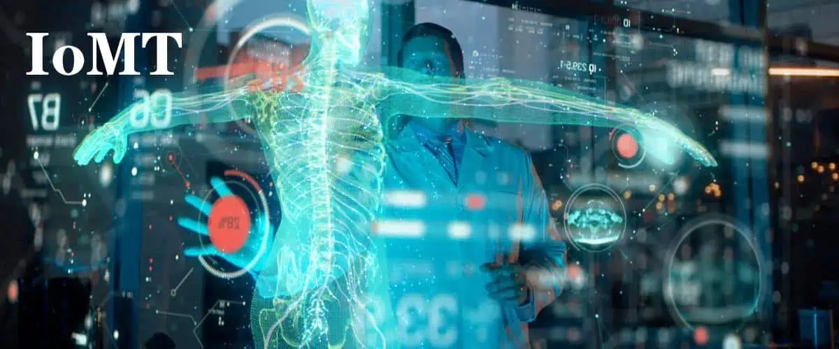
The effect of IoMT in the healthcare system has been recognized over the years. This aspect of IoT mainly focuses on medical and healthcare software applications and devices.
IoMT devices help to minimize the dependence on human intervention. Also, this subset of IoT has reduced the number of hospital visits per patient by simply connecting patients to their providers.
What is the Internet of Medical Things?
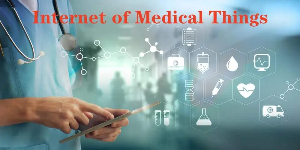
Internet of Medical Things (IoMT) deals with the medical devices and software that connect to the technology systems through the internet. IoMT is a part of the IoT technologies. It consists of internet connected applications and devices related to medical information. The Internet of Medical Things (IoMT) is very beneficial in the medical industry. IoMT devices have helped patients and doctors to stay connected, including medical devices.
Just like the usual IoT device, IoMT devices make use of sensors, machine-based intelligence, and sensors to perform their functions. Using IoMT devices in the healthcare systems helps to minimize our dependence on human intervention while routine monitoring operations are going on. Also, these devices help healthcare providers and patients to gain access to the healthcare details of a patient.
The introduction of IoMT has helped to minimize frequent visits or unnecessary visits to the hospital. Also, this type of IoT helps to minimize costs for healthcare providers and their patients. With IoTM, it is easy to transmit medical data over a network. Also, medical IoT enables remote devices and wireless devices to communicate via the internet. This enables flexible and quick analysis of medical information.
Due to the sensitivity of healthcare data, there should be a high level of security around IoMT.
Below are some scenarios that involve IoMT
- Tracking of the medication orders of patient
- Integrating remote patient monitoring (RPM) for patients that have long-term health conditions
- Gathering of data from the wearable devices of a patient
- Detecting the where patients admitted to the hospitals are
What are IoT Medical Devices?
IoT medical devices are now commonly used in the medical field. Most of these devices are wearable. They can detect health issues in the body and offer accurate data about these illnesses. IoT medical devices connect to cloud, where there are stored data. These days, healthcare practitioners now use IoT medical devices to monitor patients in their homes. This practice is what is termed telemedicine.
Telemedicine has reduced the visits of patient to a doctor’s office or a hospital. For instance, people who have asthma or diabetes can easily track their health status without any visit to the hospital. Some IoMT devices use bluetooth or apps on phone to function properly.
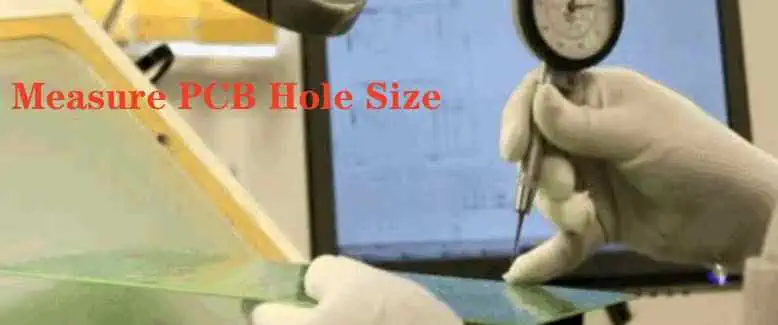
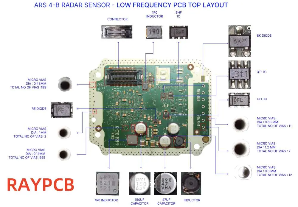
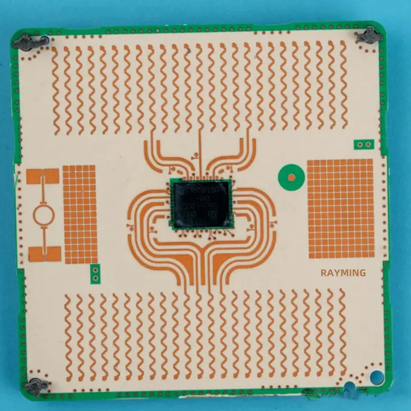
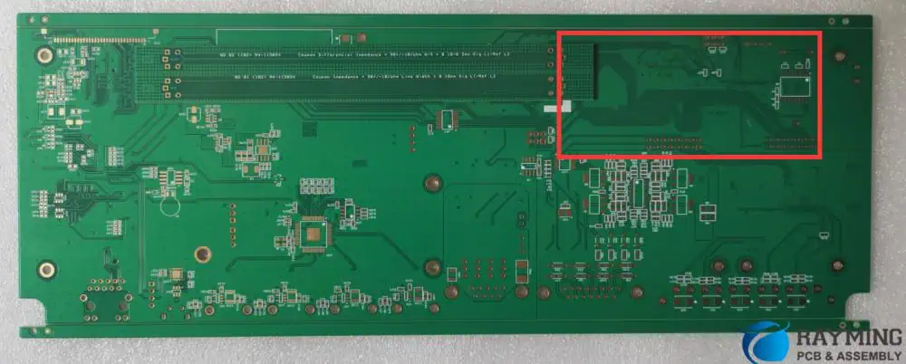
IoMT Device PCB
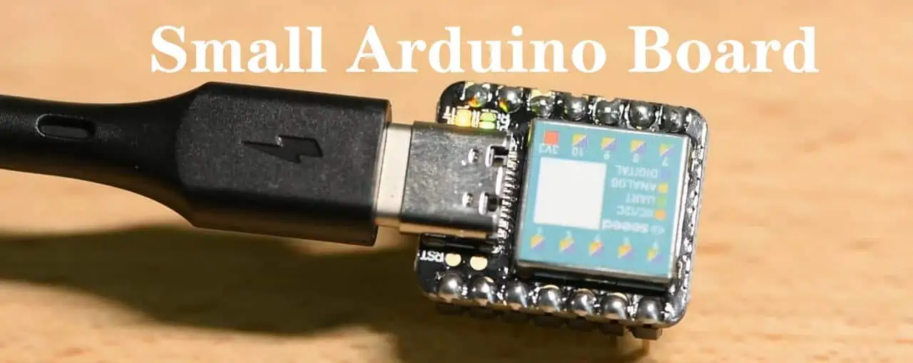
Printed circuit boards are the core of electronic devices. They are crucial in the production of IoMT devices. They enable these devices carry out the functions they are expected to. For instance, IoT medical devices like fitness trackers, glucose monitor, and heart rate monitors comprise PCBs. These devices mostly comprise flexible PCBs.
Circuit boards make it possible for new ideas to become reality, whether it is monitoring glucose levels or the symptoms of Parkinson’s disease. IoMT devices wouldn’t have been able to attain a great feat without circuit boards. These boards are used in many medical devices and wearables.
Flexible PCBs can fit into any shape. Even the smallest IoT medical device features printed circuit boards. The functionality of IoT medical devices rely on PCBs. Flexible boards and high-density interconnect (HDI) boards offer the flexibility and freedom needed by high-performance medical devices.
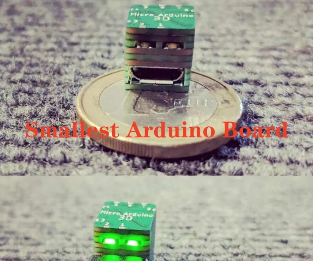
IoMT device PCBs are crucial for the functionality of IoT medical devices. These PCBs are usually smaller in size and lighter in weight. Therefore, they make it possible to design portable medical devices which can be worn around or carried about. Due to IoT, the approaches towards the design of PCBs are gradually changing. Therefore, there is the need to reduce assembly errors and optimize reliability more than ever.
When designing IoMT device PCBs, there are major things to put in mind. Since these boards are used for medical purposes, they need careful simulation and tests to ensure they are adaptable to the human body. PCB designers need to address thermal effects.
Types of IoMT Devices
IoMT devices differ based on their environment. Therefore, there are different types of IoMT devices.
Wearable IoMT
Wearable IoMT devices connect to the body of a person and take records of medical data about the person wearing them. These devices can either be medical grade or consumer grade. Smart pills and neuromodulation device are examples of medical grade wearables while smartwatches are consumer-grade IoMT devices.
In-hospital IoMT
Examples of in-hospital IoMT devices include MRI machines, infusion pumps, and hospital beds. Healthcare facilities integrate internet connectivity to provide care for patients. Also, these devices help in asset and inventory managements.
In-home IoMT
This type of IoMT devices are used around the home. For instance, RPM devices monitor patients that have critical health conditions in their homes.
Public IoMT
Public IoMT devices are used throughout a geographic location. The point-of-care kiosks that gives out medical supplies and links patients with providers is an example of public IoMT devices. They help patients who are living in remote areas have access to healthcare.
What are the Use Cases of IoMT devices?

Glucose monitoring
A large number of people now have diabetes. Diabetes is now a well-known health issue among the young and the old. It is not convenient to track glucose level manually. Most times, manual recording of glucose levels in the body is always done when some tests have been performed. Therefore, diabetic patients with fluctuating glucose level would have problem with tracking their glucose level.
IoT medical devices provide a lasting solution to this problem. There is a monitoring device which can easily alert diabetic patients when they have a rising glucose level.
Heart rate monitoring
Heart rate monitors is an example of IoT medical devices which helps in regulating the heart rate. Patients need to connect to wired machines when using traditional cardiac IoT device. This could affect quality of life and mobility negatively. However, the advent if a portable heart rate monitor can offer better monitoring. Also, patients can freely move about while their heart rates are being monitored.
Connected inhalers
Some medical conditions such as asthma attack can occur suddenly. Most times, this attack occurs without any warning. However, IoT connected inhalers can monitor the frequency of these attacks and record them. This will help providers to know what causes the attack. Also, an IoT connected inhaler can remind patients to always go with their inhalers.
IoT contact lens
IoT contact lens works well by providing more opportunities to get data. This medical device is wearable and comprises micro-cameras that can take pictures. There are patent connected contact lens by Google. Smart contact lens intends to transform the human eye.
Remote health monitoring
This is the most common use case for IoMT devices. With remote patient monitoring, providers can have access to health metrics such as body temperature, blood pressure, and heart rate. Also, patients don’t need to go to any healthcare facility to obtain this information. Remote health monitoring is beneficial to both providers and patients.
This enables patients to easily track their well-being and as well take measures to improve it. Also, healthcare practitioners can know if their patients are doing well. Furthermore, the remote patient monitoring device has reduced the need for patients to keep traveling in order to get medical information as regards their health.
Parkinson’s disease
For effective treatment of Parkinson’s disease, medical practitioners need to know how the symptoms fluctuate all through the day. There is a special IoT medical sensor designed to gather the symptom data of Parkinson’s disease.
What is the Impact of IoMT on Healthcare?
IoMT has a positive impact on healthcare in so many ways. It increases the amount of data providers can have access to. As it becomes easy to transmit data, the lives of patients will improve and providers will be able to make good decisions as regards their patient’s health.
Also, the Internet of Medical Things comprises networks and devices which allow virtual care and telemedicine to become effective. For instance, during the COVID-19 pandemic, IoMT made things easier in the health sector. It helped in reducing the number of patients that traveled to hospitals. Also, it reduced the stress on hospitals that were already burdened with cases of COVID 19.
Through IoMT, people could live their lives in remote areas and still have access to good healthcare. Furthermore, it enables people to gain access to specialists virtually. Over time, IoMT has taught us that we don’t need to have a physical meeting with healthcare practitioners before we can get treated.
Benefits of Internet of Medical Things
IoMT has been very beneficial in the healthcare system. Both healthcare practitioners and patients enjoy the benefit of IoMT. So, what are these benefits?
Patient empowerment
Patients can be in charge of their lives and regulate their vitals through IoMT devices. IoT devices like glucose monitors, remote health monitors, and more provide data concerning a patient’s health to the patient and doctor. Therefore, doctors can have access to patient’s health remotely.
Remote advice and medical treatment
The purpose of IoMT devices is to collect data from anywhere. These devices are capable of collecting data remotely. They could get data from a patient’s home and send he information to the provider. The provider can access the information and then administer treatment and offer medical advice remotely.
Accuracy
IoMT gives accurate data to medical clinicians concerning the health conditions of their patients. In the medical world, accuracy is very important. In critical health conditions, doctors need to have access to a patient’s health condition. For instance, an IoMT blood pressure monitor can offer information about the daily health rate readings and blood pressure of a patient. This information will be more accurate than data obtained from a single visit to a doctor.
Cost regulation
The cost of obtaining medical care has increased in recent years. Therefore, patients are looking for more cost-effective ways to get medical care. IoMT has provided means for patients to get such. With remote patient monitoring, a lot of money will be saved. According to prediction, about $305 billion will be saved.
Logistics
You can make use of IoT devices to regulate equipment used in hospitals. These devices will monitor equipment and then inform engineers when there are issues or when there is a need for maintenance. Also, IOMT devices can track patients and their medications.
Challenges of IoMT

The IoT technology has impacted the healthcare system in several ways. Although there are several uses of IoT medical devices, there are some challenges that come with using these devices. Understanding these challenges is important.
Security issues
Insecurity is one of the problems faced by Internet of Things. In the medical field, it is crucial to safeguard data. Therefore, healthcare facilities must ensure they maintain strict security standards as regards patient’s privacy. Medical data can expose providers to cybersecurity threats. Also, hackers can obtain credentials unlawfully in order to get drugs or medical care.
Data collection and classification
The collection and classification of data is a big challenge in IoMT. IoMT gathers various data in large amounts. It might become difficult to define what medical data comprise. IoT systems generate a lot of data, therefore before utilizing medical ecosystems, it is crucial to discuss the design of the system and the priorities that revolve around data usage and tracking.
Adoption
The Internet of Medical Things is still new in some countries. Hence, the adoption of this system can be a big challenge in the healthcare sector. It can be a difficult task and can take some time for a whole facility to adopt this new system. The installation time and cost can be a major barrier for some facilities.
Conclusion
IoMT devices have impacted the medical sector. These devices are transforming human lives as patients can now receive care remotely. Also, medical practitioners can easily and accurately diagnose illnesses. This has also reduced the overall cost incurred in getting medical care. IoT medical devices in clinical settings will continue to improve their performances. This means more improved diagnoses and faster recoveries for patients.