The Future of Automotive LiDAR: Long-Range MEMS vs. Short-Range TOF Solutions

The automotive industry stands at a technological crossroads as manufacturers grapple with choosing between two distinct LiDAR approaches for autonomous driving systems. Recent vehicle launches highlight this divide: the Yangwang U8 features RoboSense’s M1P long-range LiDAR for lateral sensing, while the AITO M series employs TOF (Time-of-Flight) solid-state LiDAR for short-range lateral detection. This fundamental choice will shape the future of autonomous vehicle perception systems.

Understanding the Technology Divide

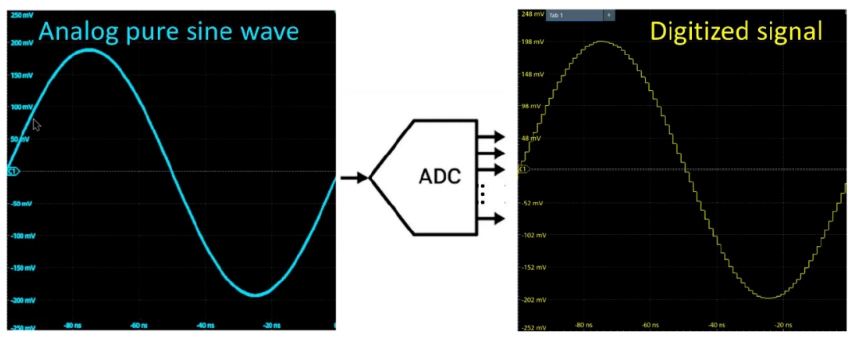
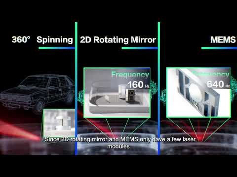
Despite both technologies being classified as “LiDAR” or “optical ranging,” they represent fundamentally different approaches to environmental perception. Long-range MEMS/solid-state LiDAR systems like RoboSense’s M1P belong to the high-performance category, delivering detailed point clouds over distances exceeding 200 meters. These systems excel at creating comprehensive 3D environmental models essential for high-speed autonomous driving scenarios.

Conversely, TOF technology operates on a simpler principle, measuring the time difference between emitted and reflected light pulses to calculate distances. While TOF sensors can be highly miniaturized and cost-effective, they typically serve short-range applications such as blind-spot monitoring, parking assistance, and low-speed collision avoidance. The key distinction lies not just in range, but in the depth and quality of environmental understanding each technology provides.

YouTube video

Performance Characteristics and Applications

Detection Range and Scenario Optimization

Long-range solid-state LiDAR systems demonstrate superior capabilities in demanding driving conditions. With detection ranges of 150-200 meters and point generation rates exceeding one million points per second, these systems provide the early warning necessary for high-speed autonomous navigation. When traveling at highway speeds, the ability to detect small objectsโ€”whether distant vehicles, pedestrians, or road debrisโ€”several seconds before potential impact becomes critical for system response time.

TOF sensors, while limited to ranges typically under 50 meters, excel in scenarios where rapid response and cost efficiency are paramount. Lane-change assistance, parking maneuvers, and blind-spot monitoring represent ideal applications for TOF technology, where ultra-low latency and compact form factors outweigh the need for long-range detection.

Point Cloud Quality and 3D Perception

The quality of environmental data represents perhaps the most significant differentiator between these technologies. Traditional high-performance LiDAR systems generate dense, three-dimensional point clouds that enable sophisticated object detection, classification, and geometric modeling. This capability proves invaluable in complex scenarios such as multi-object tracking at busy intersections, precise boundary recognition on narrow roads, or reliable obstacle detection in low-light conditions.

TOF systems typically produce 2D depth maps or sparse distance measurements rather than comprehensive 3D point clouds. While sufficient for basic proximity detection and simple geometric calculations, this limitation constrains their effectiveness in complex, far-field reasoning scenarios that autonomous vehicles regularly encounter.

Environmental Resilience and Reliability

Both technologies face challenges in adverse weather conditions, though their vulnerabilities manifest differently. Optical-based LiDAR systems can suffer from signal attenuation and false readings caused by rain, snow, or fog. However, advanced implementations incorporate dual-echo processing, extended wavelength ranges, and sophisticated signal filtering to mitigate these effects.

TOF sensors, while also susceptible to weather-related interference, benefit from their short-range focus, allowing for more targeted filtering algorithms. However, neither technology alone provides complete weather immunity, emphasizing the critical importance of multi-sensor fusion strategies that combine optical sensors with radar and camera systems.

Economic and Integration Considerations

Manufacturing and Cost Dynamics

TOF modules present compelling advantages in terms of manufacturing cost, physical size, and integration complexity. These sensors can be seamlessly embedded into vehicle designs without significant aesthetic or structural modifications, making them attractive for cost-conscious manufacturers and mainstream vehicle segments.

High-performance long-range LiDAR systems demand more sophisticated engineering, encompassing precision optics, advanced electronics, ruggedized packaging, and comprehensive safety certifications including AEC-Q100 and ISO/ASIL standards. These requirements traditionally resulted in higher costs, though economies of scale and technological maturation are driving prices downward. RoboSense’s M1 series exemplifies this trend, achieving mass production viability that makes high-performance LiDAR accessible to broader market segments.

System Architecture Philosophy

Automotive manufacturers are adopting divergent approaches based on their target market segments and technological philosophies. Premium manufacturers often center their systems around high-performance, long-range LiDAR mounted on vehicle roofs or integrated into front fascias, treating these sensors as primary perception tools supplemented by cameras and radar for redundancy and semantic understanding.

Cost-focused manufacturers prefer architectures built around camera-centric systems enhanced by strategically placed TOF sensors for specific proximity tasks. This approach leverages advanced computer vision algorithms and cloud-based data processing to achieve acceptable performance levels at significantly reduced hardware costs.

Market Segmentation and Future Trajectories

Luxury vs. Mass Market Divide

The automotive market will likely stratify along performance and price lines. Luxury and high-performance vehicles targeting Level 3+ autonomy will continue investing in long-range LiDAR systems like the M1P, prioritizing system robustness and comprehensive environmental understanding over cost considerations. These applications demand the reliability and performance that only high-end LiDAR can currently provide.

Mass-market vehicles will gravitate toward hybrid architectures combining cost-effective TOF sensors with advanced camera systems and strategic radar placement. This approach can deliver satisfactory Level 2+ functionality while maintaining price competitiveness essential for broad market adoption.

Technology Convergence and Evolution

The boundaries between these technologies continue to blur as both segments advance. Long-range LiDAR costs are declining through manufacturing scale and technological improvements, while TOF and other solid-state solutions including Optical Phased Arrays (OPA), Flash LiDAR, and Frequency Modulated Continuous Wave (FMCW) systems are extending their range and resolution capabilities.

However, fundamental physics limitations suggest that distinct functional roles will persist, with each technology optimized for specific sensing requirements rather than direct competition across all applications.

Strategic Recommendations

For Automotive Manufacturers

Vehicle manufacturers targeting Level 3+ highway autonomy should prioritize high-performance LiDAR integration for primary long-range sensing while deploying TOF sensors for blind-spot and proximity applications. This hybrid approach maximizes system capability while controlling costs through strategic sensor placement.

Manufacturers focused on cost-driven market segments should emphasize sophisticated TOF and camera fusion systems, investing heavily in software development and validation to extract maximum performance from lower-cost hardware configurations.

For System Engineers

Success lies in matching sensor capabilities to specific use cases rather than pursuing maximum technical specifications. A well-integrated, fault-tolerant system architecture that leverages the strengths of multiple sensor types will consistently outperform systems relying on single, high-specification sensors.

For Consumers

Vehicle buyers should avoid equating sensor quantity with autonomous capability. Instead, evaluate vehicles based on their comprehensive safety strategies, validation processes, and real-world performance rather than hardware specifications alone.

Conclusion: A Complementary Future

The future of automotive LiDAR will not be determined by the dominance of a single technology, but rather by the intelligent combination of complementary solutions. Long-range solid-state and MEMS LiDAR systems like RoboSense’s M1P will remain essential for high-speed autonomous driving scenarios, while TOF and short-range solutions will excel in proximity sensing and cost-sensitive applications.

This hybrid deployment strategyโ€”leveraging long-range capabilities for critical forward-facing perception and short-range sensors for comprehensive 360-degree awarenessโ€”represents the most pragmatic path forward. As hardware costs continue declining and software capabilities advance, the integration of these complementary technologies will define the next generation of autonomous vehicle perception systems.

The mainstream solution will ultimately be characterized not by technological supremacy, but by strategic deployment that matches each sensor’s strengths to specific operational requirements while maintaining the safety, reliability, and cost-effectiveness necessary for broad market adoption.

Understanding Linear Regulators: Dynamic Regulation Mechanisms and the Evolution from Three-Terminal to Advanced LDO Technology

Linear voltage regulators form the backbone of countless electronic systems, providing stable and reliable power conversion across a wide range of applications. From simple battery-powered devices to sophisticated industrial equipment, these regulators ensure that sensitive electronic components receive consistent voltage levels regardless of input variations or changing load conditions. This comprehensive analysis explores the fundamental operating principles of linear regulators, examines the key differences between traditional three-terminal regulators and low dropout (LDO) variants, and investigates the latest technological advances that are reshaping power management solutions.

YouTube video

Fundamental Architecture and Operating Principles

Linear regulators operate on two primary architectural configurations: series regulators and shunt regulators. While both serve the same fundamental purpose of voltage stabilization, series regulatorsโ€”being far more common in practical applicationsโ€”will be the focus of our discussion. These devices function as sophisticated closed-loop feedback systems that continuously monitor output conditions and dynamically adjust their internal resistance to maintain voltage stability.

The essence of linear regulation lies in its ability to act as a variable resistor that automatically adjusts its impedance in response to changing conditions. This dynamic adjustment mechanism enables the regulator to compensate for both input voltage fluctuations and load current variations, ensuring consistent output voltage delivery under diverse operating scenarios.

Dynamic Regulation During Input Voltage Variations

When examining the behavior of linear regulators under varying input conditions, the feedback control mechanism demonstrates remarkable sophistication. Consider a scenario where the input voltage experiences an increaseโ€”perhaps due to power grid fluctuations, switching noise from nearby equipment, or variations in the primary power supply. In an unregulated system, this input voltage increase would directly translate to a proportional rise in output voltage, potentially damaging sensitive downstream components.

However, in a properly designed linear regulator, the error amplifier continuously compares the actual output voltage against a stable reference voltage. When the input voltage increases, the initial tendency for the output voltage to rise is immediately detected by this error amplifier. In response, the control circuitry increases the impedance of the series pass elementโ€”effectively the variable resistor in our conceptual model.

This increased impedance serves a dual purpose: it dissipates the excess voltage differential as heat while simultaneously reducing the voltage transfer from input to output. The result is a form of “peak-clipping stabilization” where voltage spikes are absorbed by the regulator itself, maintaining a constant output voltage despite input variations. This process occurs continuously and rapidly, typically responding to input changes within microseconds.

The effectiveness of this regulation mechanism depends heavily on the design parameters of the error amplifier, including its gain bandwidth product, slew rate, and stability margins. Higher performance regulators incorporate sophisticated compensation networks and multi-stage amplification to achieve superior transient response and steady-state accuracy.

Load Current Variation Compensation

Equally important is the regulator’s ability to maintain voltage stability under changing load conditions. Modern electronic systems frequently exhibit dynamic power consumption patternsโ€”processors that switch between idle and full-load states, communication modules that transmit in bursts, or motor drives that experience varying mechanical loads.

When load current decreases, the immediate effect is a reduction in the voltage drop across the series pass element, causing the output voltage to temporarily rise above its target value. The error amplifier detects this deviation and responds by increasing the impedance of the series pass element. This compensatory action maintains the proper voltage drop even with reduced current flow, effectively preventing output voltage drift.

Conversely, when load current increases, the initial voltage drop across the series pass element rises, temporarily reducing output voltage. The error amplifier responds by decreasing the series impedance, allowing more current to flow while maintaining the desired voltage differential. This dynamic impedance adjustment ensures stable output voltage across the entire specified load current range.

The speed and accuracy of this load regulation depend on several factors, including the loop gain of the feedback system, the output capacitance, and the equivalent series resistance (ESR) of the output capacitor. Proper selection of these components is crucial for achieving optimal transient response and minimizing output voltage ripple.

Three-Terminal Regulators: Traditional Approach and Limitations

Traditional three-terminal regulators, exemplified by the ubiquitous 78xx series and similar devices, represent the foundational technology in linear voltage regulation. These regulators typically employ NPN bipolar junction transistors or N-channel MOSFETs as their series pass elements, positioned between the input and output terminals.

The fundamental limitation of three-terminal regulators lies in their relatively high dropout voltage requirements. For NPN-based designs, the minimum input-output voltage differential must satisfy the relationship: VIN – VOUT > RIN ร— IIN + 2 ร— VBE. This requirement stems from the need to maintain proper bias conditions for both the series pass transistor and the internal reference circuitry.

In practical terms, consider a typical scenario where RIN equals 1kฮฉ, input current (IIN) is 1mA, and the base-emitter voltage (VBE) is 0.7V. For a regulator designed to provide 5V output, the minimum input voltage requirement becomes 7.4V. This represents a dropout voltage of 2.4Vโ€”a significant overhead that translates directly to power dissipation and reduced efficiency.

MOSFET-based three-terminal regulators offer modest improvement, with the dropout voltage determined by VIN – VOUT > RIN ร— IIN + VGS. Using similar component values but with VGS = 1V, the minimum input voltage becomes 7V, representing a 0.4V improvement over the bipolar design.

While these dropout voltage requirements may seem manageable in high-voltage applications, they become increasingly problematic as system voltages decrease. In battery-powered applications, where maximizing operational time is critical, these relatively high dropout voltages represent significant inefficiency and reduced battery utilization.

LDO Regulators: Advancing the Technology

Low Dropout (LDO) regulators address the fundamental limitations of three-terminal regulators through innovative circuit topologies and component selection. The key breakthrough lies in their use of PNP bipolar transistors or P-channel MOSFETs as series pass elements, fundamentally altering the dropout voltage characteristics.

In PNP-based LDO designs, the minimum dropout voltage is determined by the collector-emitter saturation voltage (VCE(sat)), typically ranging from 0.1V to 0.3V depending on the specific transistor characteristics and operating current. This represents a dramatic improvement over traditional designs, enabling effective regulation even when input and output voltages are closely matched.

P-channel MOSFET implementations offer even better performance, with dropout voltages determined by the drain-source resistance (RDS(ON)) multiplied by the drain current (VDS = RDS(ON) ร— ID). Modern P-channel MOSFETs can achieve RDS(ON) values below 100 milliohms, resulting in dropout voltages well under 100mV at moderate current levels.

The practical implications of these improvements are substantial. An LDO regulator can maintain 3.3V output with input voltages as low as 3.5V, compared to traditional regulators that might require 5V or higher. This capability is particularly valuable in battery-powered applications, where it enables utilization of a greater portion of the battery’s capacity.

Beyond the primary advantage of reduced dropout voltage, LDO regulators typically offer superior line and load regulation, lower output noise, and better transient response compared to their three-terminal counterparts. These improvements stem from more sophisticated internal circuitry, including enhanced error amplifiers, improved reference voltage sources, and optimized compensation networks.

Next-Generation LDO Technology: N-Channel MOSFET Innovation

The evolution of LDO technology continues with the development of advanced regulators that push dropout voltage performance even further. These next-generation devices achieve their superior performance through the innovative use of N-channel MOSFETs, which inherently offer lower on-resistance compared to P-channel devices of equivalent size and cost.

The physics behind this advantage lies in the fundamental differences between electron and hole mobility in silicon. N-channel MOSFETs, which rely on electron conduction, can achieve significantly lower RDS(ON) values than P-channel devices, which depend on hole conduction. This translates directly to lower dropout voltages and reduced power dissipation.

However, implementing N-channel MOSFETs in LDO applications presents significant design challenges. Unlike P-channel devices that can be directly connected between input and output, N-channel MOSFETs require gate voltages higher than the input voltage to achieve proper conduction. This necessitates sophisticated control circuitry, including charge pump circuits or bootstrap techniques to generate the required gate drive voltage.

Modern implementations address these challenges through integrated solutions that combine the N-channel MOSFET with dedicated driver circuitry and auxiliary power supplies. These designs typically include separate bias voltage sources, ensuring stable operation across the full input voltage range while maintaining the low dropout advantages.

Advanced LDO Features and Performance Characteristics

Contemporary LDO regulators incorporate numerous advanced features that extend their applicability and improve system-level performance. Current limiting protection prevents device damage during short-circuit conditions, while thermal shutdown circuitry provides additional safety margins during high-temperature operation.

Many modern LDOs include enable/disable functionality, allowing system-level power management and sequencing control. This feature is particularly valuable in complex systems where different circuit blocks must be powered up or down in specific sequences to prevent latch-up or other undesirable conditions.

Noise performance represents another critical advancement area. High-performance LDOs achieve output noise levels below 50ยตVRMS across the audio frequency spectrum, making them suitable for sensitive analog applications including precision measurement systems and high-resolution data acquisition circuits.

Practical Applications and Selection Considerations

The choice between traditional three-terminal regulators, standard LDOs, and advanced N-channel LDOs depends on specific application requirements. Three-terminal regulators remain cost-effective solutions for high-voltage applications where dropout voltage is not critical, such as transforming 12V supplies to 5V logic levels.

Standard LDO regulators excel in battery-powered applications, precision analog circuits, and any scenario where input-output voltage differentials are small. Their superior regulation performance and low noise characteristics make them ideal for powering sensitive analog front-ends, precision references, and low-noise amplifiers.

Advanced N-channel LDO regulators find applications in the most demanding scenarios, such as point-of-load regulation in high-performance processors, battery-powered wireless communication systems, and portable medical devices where maximum efficiency and minimum dropout voltage are paramount.

Conclusion

The evolution from traditional three-terminal regulators to advanced LDO technology represents a significant advancement in power management capabilities. Through innovative circuit topologies, advanced semiconductor processes, and sophisticated control techniques, modern LDO regulators deliver unprecedented performance levels that enable new categories of electronic systems.

As electronic devices continue to demand lower operating voltages, higher efficiency, and improved performance, LDO regulator technology will undoubtedly continue evolving. Future developments may include adaptive dropout voltage control, integrated power monitoring, and even greater integration with digital control systems, further expanding the role of linear regulators in modern electronic design.

Understanding these technologies and their trade-offs enables engineers to make informed decisions when selecting power management solutions, ultimately leading to more efficient, reliable, and capable electronic systems.

How to Choose Between Arduino and Raspberry Pi for Beginners: A Comprehensive Guide

In the world of electronics and embedded systems, two names consistently emerge as the most popular choices for beginners and professionals alike: Arduino and Raspberry Pi. These development boards have revolutionized the way we approach hardware prototyping, IoT projects, and educational electronics. While both platforms serve the maker community exceptionally well, they represent fundamentally different approaches to computing and hardware interaction.

YouTube video

Arduino and Raspberry Pi each occupy distinct positions in the electronics ecosystem, with performance characteristics that vary significantly based on their intended use cases. The landscape became even more interesting recently when Arduino announced the Portenta X8 and Max Carrier, featuring a pre-installed Linux operating system that brings Arduino’s capabilities closer to traditional computing platforms like the Raspberry Pi. This development has sparked renewed debate about which platform beginners should choose for their first foray into electronics and programming.

Understanding the differences between these platforms is crucial for making an informed decision that aligns with your project goals, learning objectives, and technical requirements. This comprehensive guide will explore every aspect of both platforms to help you make the right choice.

The Origins and Philosophy Behind Each Platform

Arduino: Born from Educational Necessity

Arduino’s story begins in the vibrant academic environment of Italy. The platform was conceived by Massimo Banzi and his co-founders during a casual conversation in a bar โ€“ the very establishment that would later lend its name to this revolutionary platform. Banzi, who served as a teacher at the prestigious Interaction Design Institute, identified a significant gap in the available tools for hardware education. Students needed a simple, accessible way to create hardware prototypes without getting bogged down in the complexities of traditional microcontroller programming.

The Arduino philosophy centers on simplicity and accessibility. From its inception, the platform was designed to lower the barriers to entry for hardware development, making it possible for artists, designers, and hobbyists with limited technical backgrounds to bring their creative ideas to life. This educational focus is evident in every aspect of Arduino’s design, from its intuitive programming environment to its extensive documentation and community support.

Raspberry Pi: Democratizing Computer Science Education

The Raspberry Pi emerged from the prestigious halls of Cambridge University, where Eben Upton and his colleagues at the Computer Laboratory observed a concerning trend: fewer students were applying to computer science programs, and those who did often lacked fundamental programming and hardware skills. The team recognized that the increasing cost and complexity of computers had created a barrier that prevented young people from experimenting with programming and electronics.

Their solution was radical: create an entire computer that would be so affordable and accessible that every student could have one. The Raspberry Pi represents a complete departure from traditional educational computers, offering full computing capabilities in a package smaller than a credit card. This philosophy of democratizing access to computing power has made the Raspberry Pi not just an educational tool, but a platform that has enabled countless innovative projects worldwide.

Fundamental Architectural Differences

Arduino: The Dedicated Microcontroller Approach

At its core, Arduino is built around microcontroller architecture. A microcontroller is essentially a single integrated circuit that contains a processor, memory, and programmable input/output peripherals all on one chip. Think of Arduino as being similar to a single, specialized module within a larger computer system โ€“ it’s designed to excel at specific, well-defined tasks rather than general-purpose computing.

This microcontroller foundation gives Arduino several inherent advantages. When you power on an Arduino, it immediately begins executing your program without any boot process or operating system overhead. This instant-on capability makes Arduino ideal for applications that need to respond quickly and reliably to sensor inputs or control hardware components. The dedicated nature of the system means that all processing power is focused on your specific application, without competing system processes consuming resources.

Raspberry Pi: The Complete Computer Solution

The Raspberry Pi takes a fundamentally different approach, built around a microprocessor architecture similar to what you’d find in a desktop computer or smartphone. This system-on-chip design includes not just a processing unit, but also graphics processing capabilities, multiple types of memory, and sophisticated input/output systems. The result is essentially a fully functional computer that happens to be incredibly small and affordable.

This complete computer approach enables the Raspberry Pi to run full operating systems like Linux distributions or even Windows 10 IoT. With an operating system comes the ability to run multiple programs simultaneously, connect to networks, browse the internet, and perform complex computational tasks that would be impossible or impractical on a microcontroller platform.

Detailed Technical Specifications and Performance Analysis

When examining the technical specifications of these platforms, the differences become immediately apparent and help explain their different use cases and capabilities.

The Raspberry Pi 2, for example, operates with a quad-core ARM Cortex-A7 processor running at 900MHz, supported by 1GB of RAM and the ability to run from microSD cards with capacities up to 32GB or more. This configuration provides computational power that rivals entry-level desktop computers from just a few years ago. The inclusion of multiple USB ports, HDMI output, Ethernet connectivity, and built-in Wi-Fi capabilities makes it a truly versatile computing platform.

In contrast, Arduino boards typically feature much more modest specifications that reflect their focused mission. A standard Arduino Uno operates with an 8-bit microcontroller running at 16MHz, with just 32KB of flash memory for program storage and 2KB of RAM for variables. While these numbers might seem limiting compared to the Raspberry Pi, they’re perfectly adequate for the real-time control tasks that Arduino excels at.

The performance gap between these platforms is significant in terms of raw computational power, but it’s important to understand that this gap exists by design. Arduino’s lower-powered approach results in several practical advantages: much lower power consumption, more predictable real-time behavior, and simpler programming models that are easier for beginners to understand and debug.

Software Ecosystems and Programming Environments

Raspberry Pi: Full-Featured Computing Environment

The Raspberry Pi’s ability to run complete operating systems opens up a world of software possibilities that simply aren’t available on microcontroller platforms. With a Linux-based operating system, users have access to thousands of pre-built software packages, powerful development environments, and the ability to use virtually any programming language.

Python has become particularly popular on the Raspberry Pi platform, thanks to its beginner-friendly syntax and extensive libraries for hardware control, data analysis, and network communication. However, the platform equally supports C/C++, Java, JavaScript, and dozens of other programming languages. This flexibility makes the Raspberry Pi an excellent choice for projects that require complex algorithms, data processing, machine learning capabilities, or integration with web services and databases.

The trade-off for this software richness is complexity. Setting up a Raspberry Pi project typically involves installing an operating system, configuring software packages, and writing programs that must coexist with other system processes. While this mirrors real-world software development practices, it can be overwhelming for absolute beginners.

Arduino: Streamlined Development Experience

Arduino’s software approach prioritizes simplicity and immediate results. The Arduino IDE (Integrated Development Environment) provides a clean, straightforward interface for writing, compiling, and uploading code to the hardware. The programming language is based on C/C++ but includes many simplifications and abstractions that make it more accessible to beginners.

One of Arduino’s greatest strengths is its vast library ecosystem. Need to control a servo motor? There’s a library for that. Want to read data from a temperature sensor? Another library handles the complex communication protocols for you. This extensive library support means that beginners can accomplish sophisticated tasks with just a few lines of code, building confidence and enabling rapid prototyping.

The Arduino programming model is also inherently simpler because there’s no operating system to manage. Your program has complete control over the hardware, and the execution model is straightforward: setup runs once when the device powers on, and loop runs continuously afterward.

Hardware Integration and Connectivity

Arduino: Purpose-Built for Hardware Control

Arduino’s design philosophy shines brightest when it comes to hardware integration. The platform was specifically engineered to make connecting sensors, motors, LEDs, and other electronic components as straightforward as possible. Most Arduino boards feature clearly labeled pins that can be easily connected to external components using simple jumper wires or breadboards.

The real-time nature of Arduino’s microcontroller means it can respond to sensor inputs within microseconds, making it ideal for applications that require precise timing or immediate responses to changing conditions. Whether you’re reading data from multiple sensors simultaneously, controlling servo motors with precise positioning, or managing LED displays, Arduino handles these tasks with reliability and simplicity that’s hard to match.

Arduino’s analog-to-digital conversion capabilities are also noteworthy. Many Arduino boards include multiple analog input pins that can directly read varying voltage levels from sensors like light detectors, temperature sensors, or potentiometers. This capability eliminates the need for additional conversion hardware that other platforms might require.

Raspberry Pi: Computational Power with Hardware Access

While the Raspberry Pi is primarily a computing platform, it doesn’t neglect hardware connectivity. The GPIO (General Purpose Input/Output) pins provide access to the underlying hardware, allowing users to control LEDs, read sensors, and communicate with other electronic devices. However, the approach is necessarily different from Arduino’s direct hardware control.

On the Raspberry Pi, hardware interaction typically occurs through the operating system, which means your programs must request permission to access hardware resources and may experience delays if the system is busy with other tasks. For many applications, these delays are imperceptible and don’t cause problems. However, for applications requiring precise timing or real-time responses, this can be a significant limitation.

The Raspberry Pi’s strength in hardware projects lies in its ability to process and analyze the data it collects. Where Arduino might struggle with complex calculations or data storage, the Raspberry Pi can easily handle tasks like image processing, data logging to files or databases, or sending information over network connections.

Practical Applications and Project Examples

Arduino Project Scenarios

Arduino excels in projects that focus on direct hardware control and real-time responses. Consider a home automation system that monitors temperature and humidity while controlling heating and cooling systems. Arduino can continuously read sensor values, make immediate decisions about when to activate or deactivate systems, and maintain precise control over the environment without any delays or interruptions.

Robotics projects also benefit tremendously from Arduino’s real-time capabilities. A robot that needs to avoid obstacles, follow lines, or respond to remote control commands requires the instant response times that Arduino provides. The platform’s extensive library of motor control, sensor reading, and communication functions makes it possible to build sophisticated robotic systems with relatively simple code.

Raspberry Pi Project Scenarios

The Raspberry Pi shines in applications that require significant computational power, network connectivity, or complex user interfaces. A home security system that captures video from multiple cameras, performs facial recognition, sends alerts via email or text message, and provides a web interface for remote monitoring plays to all of the Raspberry Pi’s strengths.

Data logging and analysis projects also benefit from the Raspberry Pi’s capabilities. Environmental monitoring systems that collect data from multiple sensors, store the information in databases, perform statistical analysis, and generate reports or visualizations are well-suited to the platform’s computing power and storage capabilities.

The Power of Integration: Using Both Platforms Together

One of the most powerful approaches to complex projects involves using both Arduino and Raspberry Pi in complementary roles. In this configuration, Arduino handles the real-time hardware control tasks while the Raspberry Pi manages higher-level processing, data storage, and network communication.

Consider a sophisticated weather monitoring system: Arduino boards at various locations could continuously read temperature, humidity, wind speed, and other sensor data, then transmit this information to a central Raspberry Pi system. The Raspberry Pi would store the data in a database, perform analysis to identify trends and patterns, generate weather forecasts using machine learning algorithms, and provide a web interface that allows users to view current conditions and historical data from anywhere in the world.

This division of labor leverages the strengths of both platforms while minimizing their respective weaknesses. Arduino ensures reliable, real-time data collection without interruption, while the Raspberry Pi provides the computational power needed for complex analysis and the connectivity required for remote access.

Making the Right Choice for Your Journey

The decision between Arduino and Raspberry Pi ultimately depends on your specific goals, interests, and the types of projects you want to pursue. If your primary interest lies in building interactive physical projects, controlling motors and sensors, or learning the fundamentals of embedded programming, Arduino provides an excellent starting point. Its simplicity, immediate feedback, and focus on hardware interaction make it ideal for building confidence and developing fundamental skills.

Conversely, if you’re drawn to projects involving data analysis, network connectivity, computer vision, or artificial intelligence, the Raspberry Pi offers capabilities that Arduino simply cannot match. Its full computing environment also makes it valuable for learning general programming skills that transfer directly to other computing contexts.

For beginners who are unsure about their long-term interests, Arduino often provides a gentler introduction to the world of electronics and programming. Its focused scope means fewer concepts to master initially, while still providing a foundation that makes transitioning to more complex platforms easier when the time comes.

Remember that choosing one platform doesn’t preclude using the other in the future. Many successful makers and engineers use both platforms regularly, selecting the right tool for each specific project’s requirements. The skills and concepts learned on either platform provide valuable preparation for working with the other, making your initial choice less critical than simply getting started with hands-on learning and experimentation.

Securing the Future: Building Robust Cybersecurity for Modern Robot Control Systems

ADI explores critical security vulnerabilities and comprehensive safety measures essential for next-generation robotics infrastructure

Introduction: The Cybersecurity Imperative in Industry 4.0

The modern industrial landscape is undergoing a dramatic transformation driven by Industry 4.0, where intelligent automation has become the cornerstone of manufacturing excellence. At the center of this revolution stand industrial robots, autonomous mobile robots (AMRs), and collaborative robots (cobots), each playing increasingly sophisticated roles in realizing our connected industrial future.

Today’s robots have evolved far beyond their mechanical predecessors. They possess enhanced artificial intelligence, advanced collaborative capabilities, and the ability to execute complex tasks with minimal human oversight. This evolution has propelled robotics beyond traditional factory floors into critical sectors including healthcare, logistics, agriculture, and public infrastructure. However, with this expanded adoption comes an equally expanded attack surface that cybercriminals are eager to exploit.

While operational accidents in robotics are manageable through established safety protocols, cyberattacks present an entirely different category of risk. When malicious actors successfully hijack robot control systems, the consequences extend far beyond operational disruption. These attacks can result in catastrophic equipment damage, compromised product quality, stolen intellectual property, and in worst-case scenarios, physical harm to human operators. The financial implications alone can reach millions of dollars, making cybersecurity not just a technical consideration but a business-critical imperative.

Understanding the Threat Landscape: Critical Security Vulnerabilities

The security challenges facing modern robot control systems are multifaceted and constantly evolving. Attackers employ increasingly sophisticated methods to identify and exploit vulnerabilities across multiple attack vectors, from network communications to embedded hardware components.

Network Security Deficiencies

Communication infrastructure represents one of the most vulnerable aspects of robot control systems. Without proper security protocols, data transmission between robots, controllers, and management systems becomes susceptible to a range of attacks. Malicious actors can intercept sensitive operational data, inject false commands, or completely disrupt system communications. The interconnected nature of modern robotics means that a single compromised communication channel can provide access to entire production networks.

Authentication and Access Control Weaknesses

Many robot systems continue to rely on default credentials or weak authentication mechanisms, creating easily exploitable entry points for attackers. The proliferation of connected devices and peripherals in modern robotics environments compounds this problem. Without robust device authentication, systems may unknowingly accept input from counterfeit sensors, compromised controllers, or entirely malicious devices masquerading as legitimate system components.

Data Protection and Confidentiality Gaps

Robot systems generate and store vast amounts of sensitive data, including proprietary manufacturing processes, quality control parameters, and operational patterns. When this information lacks proper encryption protection, it becomes vulnerable to interception and theft. Industrial espionage through robot systems has become a significant concern, particularly for companies developing competitive technologies or serving government contracts.

Integrity and Secure Update Challenges

The integrity of robot firmware and software represents another critical vulnerability. Without secure boot processes and update mechanisms, attackers can modify system software, install malicious code, or roll back systems to versions with known vulnerabilities. This type of attack is particularly insidious because it can operate undetected for extended periods while gathering intelligence or slowly degrading system performance.

Hardware-Level Security Concerns

Modern robots often store highly sensitive configuration data, cryptographic keys, and proprietary algorithms directly in their control systems. Without tamper-resistant hardware protection, this information remains vulnerable to physical attacks. Sophisticated attackers can extract sensitive data through invasive hardware analysis, potentially compromising not just individual systems but entire product lines or manufacturing processes.

Legacy System Integration Problems

The industrial robotics sector has historically prioritized functionality and reliability over security. Many existing systems were designed during an era when cybersecurity was not a primary concern, creating architectural vulnerabilities that are difficult to address through software updates alone. These legacy systems often become the weakest links in otherwise secure networks.

Regulatory Evolution: Driving Cybersecurity Standards Forward

The rapidly evolving cybersecurity threat landscape has prompted significant regulatory response across major industrial markets. The European Union’s Cybersecurity Act and the emerging Cyber Resilience Act establish comprehensive frameworks for industrial cybersecurity, while the United States continues to strengthen critical infrastructure protection through legislation like the Critical Infrastructure Cyber Incident Reporting Act.

Asian markets are following suit, with China and India continuously refining their cybersecurity regulations to address emerging threats. This global regulatory convergence is creating unprecedented pressure on robotics manufacturers to implement robust security measures from the design phase forward.

IEC 62443: The Gold Standard for Industrial Security

Among the various standards and guidelines available, IEC 62443 has emerged as the definitive framework for Industrial Automation and Control Systems (IACS) security. This comprehensive standard provides systematic guidance for implementing “secure-by-design” principles throughout the development lifecycle.

IEC 62443’s component-focused sections, particularly IEC 62443-4-1 and IEC 62443-4-2, directly address the security requirements for software applications, host devices, embedded devices, and network components commonly found in robot control systems. The standard defines four Security Levels (SL0โ€“SL3) based on specific Component Requirements (CR) and Enhancement Requirements (RE), with SL2 and SL3 explicitly mandating hardware-based security mechanisms.

Compliance with IEC 62443 not only helps organizations meet regulatory requirements but also provides a structured approach to identifying, assessing, and mitigating cybersecurity risks. This standardized framework enables consistent security implementation across different robot platforms and manufacturers.

Essential Technologies for Secure Robot Systems

Building truly secure robot control systems requires a multi-layered approach that addresses vulnerabilities at every level of the system architecture. The following technologies and capabilities form the foundation of robust robot cybersecurity:

Advanced Authentication Systems

Secure authentication goes beyond simple password protection to include cryptographic device identification and multi-factor verification. Modern robot systems require the ability to verify the identity of every connected component, from sensors and actuators to network interfaces and human machine interfaces. Hardware-based authenticators provide tamper-resistant credential storage and cryptographic operations that software-only solutions cannot match.

Dedicated Security Coprocessors

Specialized security hardware, such as secure coprocessors and cryptographic engines, provides isolated environments for sensitive operations. These components handle encryption, decryption, digital signature generation, and key management operations independently from main system processors, preventing compromised application software from accessing critical security functions.

Encrypted Communication Protocols

All data transmission within robot systems must be protected through strong encryption protocols. This includes not only external network communications but also internal communications between system components. Modern encryption standards and key management practices ensure that intercepted communications remain useless to attackers.

Granular Access Control

Fine-grained permission systems enable precise control over who can access specific system functions and data. Role-based access control (RBAC) and attribute-based access control (ABAC) systems ensure that users and processes receive only the minimum privileges necessary for their designated functions.

Physical Security Measures

Comprehensive security requires protection against physical tampering attempts. This includes tamper-evident packaging, secure enclosures, and hardware security modules (HSMs) that can detect and respond to physical intrusion attempts.

Secure Development Lifecycle Integration

Security cannot be an afterthought in robot system development. A structured Security Development Lifecycle (SDL) ensures that security considerations are embedded throughout the development process, from initial requirements gathering through deployment, maintenance, and eventual decommissioning.

ADI’s Comprehensive Security Partnership

Analog Devices Inc. (ADI) brings decades of security expertise and practical implementation experience to the robotics industry. Rather than simply providing discrete security components, ADI offers comprehensive solutions that address the full spectrum of robot security challenges.

The company’s approach extends beyond traditional component supply to include system-level security architecture consulting, implementation guidance, and ongoing support. This holistic perspective ensures that security measures integrate seamlessly across hardware, software, and communication layers.

Proven Automotive Security Experience

ADI’s wireless Battery Management System (wBMS), developed through extensive collaboration with automotive industry leaders, demonstrates the company’s capability to implement sophisticated security measures in safety-critical applications. The ISO 21434-certified wBMS incorporates multiple layers of security protection, from secure boot processes to encrypted wireless communications.

This automotive experience directly translates to robotics applications, where similar requirements for safety, reliability, and security convergence exist. The lessons learned from implementing security in high-volume, cost-sensitive automotive applications provide valuable insights for robotics manufacturers facing similar challenges.

Integrated Hardware and Software Solutions

ADI’s security offerings include both turnkey hardware solutions, such as the MAXQ1065 authenticator and DS28S60 coprocessor, and comprehensive software protocol stacks for host processors. This integrated approach enables customers to implement security measures appropriate to their specific requirements and constraints.

The discrete security elements provide enhanced resilience by isolating sensitive credentials and cryptographic operations in physically separate integrated circuits. Even if application processors become compromised, these dedicated security devices continue to protect critical system functions.

Real-World Implementation: Robot Joint Controller Security

A practical example of security implementation can be seen in robot joint control systems, where the MAXQ1065 security IC demonstrates clear value in enabling secure boot processes and enhancing overall system security. This application showcases how dedicated security hardware can provide secure key storage, encrypted communication capabilities, and robust cryptographic operations without impacting real-time control performance.

The integration of security hardware at the joint controller level ensures that even individual robot components maintain security integrity, creating a distributed security architecture that remains resilient even if higher-level systems are compromised.

Conclusion: Securing Robotics’ Future

The future of robotics depends fundamentally on our ability to implement and maintain robust cybersecurity measures. As robots become increasingly intelligent and interconnected, the potential impact of successful cyberattacks will continue to grow. However, by implementing comprehensive security frameworks that include secure authentication, encrypted communication, tamper-resistant hardware, and supply chain security measures, we can unlock robotics’ full potential while effectively managing cybersecurity risks.

The convergence of regulatory requirements, technological capabilities, and practical implementation experience creates an unprecedented opportunity to build security into the foundation of next-generation robotics systems. Organizations that embrace this security-first mindset will not only protect their operations from cyber threats but will also gain competitive advantages through improved reliability, compliance, and customer trust.

Success in this endeavor requires partnerships with experienced security specialists who understand both the technical challenges and business imperatives of modern robotics. By leveraging proven security technologies and implementation methodologies, the robotics industry can confidently navigate the cybersecurity challenges ahead while continuing to drive innovation and operational excellence.

The journey toward comprehensive robot security begins with recognizing cybersecurity as a fundamental design requirement rather than an optional enhancement. With the right approach, technologies, and partnerships, we can ensure that tomorrow’s robots are not only more capable but also more secure than ever before.

Open-Source Hardware/Software Project: Infrared Remote Gateway (IRext)

Comprehensive IR Code Library + Remote Control for AC Units + Advanced IR Learning Functionality

1. Introduction and Problem Statement

The evolution of smart homes has transformed how we interact with our living spaces, yet one significant challenge persists: the integration of legacy infrared-controlled devices into modern smart ecosystems. This challenge is particularly pronounced with air conditioning units, where the diversity of infrared protocols creates a fragmented user experience that undermines the promise of seamless home automation.

YouTube video

Contemporary households often accumulate multiple infrared remotes, each dedicated to specific appliances from different manufacturers. This proliferation stems from the lack of standardization in infrared communication protocols across brands. Each manufacturer implements proprietary encoding schemes, carrier frequencies, and command structures, making universal control a complex engineering challenge. The situation becomes more complicated when considering that many existing AC units, especially those installed in residential and commercial buildings over the past decades, lack network connectivity capabilities essential for modern smart home integration.

While numerous smart control applications exist in the market, they typically require devices to have built-in network supportโ€”WiFi, Bluetooth, or other communication protocols. This prerequisite excludes millions of older AC units that rely solely on infrared communication, creating a significant gap in smart home adoption and forcing users to either replace functional equipment or accept a fragmented control experience.

The IRext Solution

Our project addresses these challenges through a comprehensive gateway solution that serves as a universal translator between legacy infrared devices and modern smart home ecosystems. The system combines hardware engineering with open-source software libraries to create a bridge that enables remote control of most AC brands through infrared signals, enhanced with sophisticated IR learning capabilities.

The design philosophy prioritizes reliability, efficiency, and accessibility. Rather than developing another proprietary solution, we’ve embraced open-source principles to ensure the project can evolve through community contributions and remain accessible to developers, hobbyists, and manufacturers worldwide.

Strategic Design Decisions

The architecture reflects careful consideration of real-world deployment requirements. Ethernet connectivity was chosen over WiFi for several critical reasons: superior stability in industrial and residential environments, lower power consumption during continuous operation, and reduced susceptibility to interference from other wireless devices. This decision particularly benefits users with older homes where WiFi signals may be inconsistent or where network reliability is paramount.

The hardware foundation centers on WIZnet’s W55MH32 microcontroller unit, which integrates a complete TCP/IP stack alongside MAC and PHY layers. This integration eliminates the complexity and potential reliability issues associated with external network interface controllers, while providing hardware-accelerated networking that ensures low-latency communication essential for responsive device control.

The user interface leverages WeChat Mini Programs, eliminating the need for dedicated app installations while providing cross-platform accessibility. This approach recognizes the reality that users prefer solutions that integrate with platforms they already use daily, reducing barriers to adoption and ongoing engagement.

Local storage utilizes W25Q64 flash memory organized through the FatFs file system, ensuring learned IR codes remain accessible even during network outages. This design decision reflects the principle that smart home devices should maintain core functionality regardless of cloud service availability.

2. Technical Deep Dive: Infrared Technology and Implementation

Understanding Infrared Communication Protocols

Infrared remote control technology relies on modulated light signals operating in the near-infrared spectrum, typically around 940 nanometers. The fundamental principle involves encoding digital information through precisely timed bursts of infrared light at specific carrier frequencies, most commonly 38kHz or 56kHz depending on the manufacturer and application.

The encoding process transforms binary data into temporal patterns where logic states are represented by different combinations of carrier presence and absence. The widely-adopted NEC protocol, for example, uses a distinctive start sequence of 9000 microseconds of carrier signal followed by 4500 microseconds of silence to establish synchronization between transmitter and receiver. Individual bits are then encoded using shorter timing patterns, where a logic ‘0’ might consist of 562.5 microseconds of carrier followed by 562.5 microseconds of silence, while a logic ‘1’ extends the silence period to 1687.5 microseconds.

These timing requirements demand precise control from both hardware and software perspectives. Microcontroller implementations must maintain accuracy within microsecond tolerances while managing other system functions, requiring careful attention to interrupt handling, timer configuration, and real-time constraints.

IRext Library Integration and Capabilities

The IRext open-source universal IR code library represents a collaborative effort to standardize infrared device control across manufacturers and regions. The library’s comprehensive database encompasses over 1,000 brands spanning 16 distinct device categories, with detailed support for more than 10,000 individual device models. This extensive coverage results from community contributions and systematic reverse engineering of proprietary protocols.

The library architecture accommodates both online and offline deployment scenarios. Online implementations can access continuously updated code databases through API calls, ensuring compatibility with newly released devices. Offline implementations download complete brand-specific databases for local storage, enabling operation in environments with limited or unreliable internet connectivity.

Resource optimization receives particular attention, recognizing that many deployment scenarios involve constrained embedded systems. The library includes variants optimized for 8-bit microcontrollers with limited memory, employing compression algorithms and efficient data structures to minimize storage and processing requirements while maintaining full functionality.

Implementation Strategies and Code Integration

The integration process involves multiple layers of abstraction designed to simplify developer interaction while maintaining flexibility for advanced use cases. The file system decoding approach provides the most straightforward implementation path:

// Initialize IR library with file system support
ir_file_open(category, sub_category, "brand_specific_codes.bin");

// Decode specific command with current AC status
result = ir_decode(key_code, user_data_buffer, &ac_status, change_wind_direction);

// Clean up resources
ir_close();

Memory decoding offers enhanced performance for applications requiring rapid command execution or operating under real-time constraints:

// Load IR codes directly into memory buffer
ir_binary_open(category, sub_category, code_buffer, buffer_length);

// Perform decoding operation
result = ir_decode(key_code, output_buffer, &ac_status, parameter_changes);

// Release memory resources
ir_close();

Current library capabilities focus on essential AC control functions including power state management, fan speed adjustment, temperature setting, and swing mode control. However, the extensible architecture facilitates addition of device-specific features and advanced control modes as the library evolves.

3. Comprehensive Software Architecture

Mini Program Communication Infrastructure

The communication architecture implements a robust three-tier approach connecting user interfaces to hardware through reliable cloud intermediation. The WeChat Mini Program serves as the primary user interface, leveraging familiar interaction paradigms while eliminating app installation friction. The OneNET cloud platform provides reliable message routing through HTTP APIs, transforming user interactions into MQTT messages suitable for IoT device communication.

This architecture offers several advantages over direct device communication approaches. Cloud intermediation enables remote access regardless of network topology, supports multiple concurrent users, and provides logging and analytics capabilities essential for system monitoring and troubleshooting. The HTTP-to-MQTT translation layer accommodates the stateless nature of web-based interfaces while maintaining the persistent connections required for responsive device control.

Message formatting utilizes JSON structures designed for both human readability and efficient parsing on resource-constrained devices:

json

{
  "id": "unique_command_identifier",
  "timestamp": "2024-08-08T15:30:00Z",
  "params": {
    "Command": "Control",
    "AC": {
      "ACBrand": 0,
      "ACType": 1,
      "openFlag": 1,
      "modeGear": 2,
      "temperature": 25,
      "fanSpeed": 1,
      "operation": 3,
      "swingMode": 0
    }
  }
}

MQTT Implementation and State Management

The MQTT protocol provides reliable, low-overhead communication suitable for IoT applications with varying network conditions. The implementation maintains persistent connections through sophisticated state management that handles network interruptions, broker failures, and device restarts gracefully.

Topic structure follows OneNET conventions while allowing for extensibility:

  • Subscription: $sys/{project_id}/{device_name}/thing/property/set
  • Response: $sys/{project_id}/{device_name}/thing/property/set_reply
  • Status: $sys/{project_id}/{device_name}/thing/property/post

The state machine implementation manages connection establishment, authentication, subscription management, and keepalive signaling. Error recovery mechanisms include exponential backoff for reconnection attempts, duplicate message detection, and graceful degradation during extended outages.

4. Hardware Implementation and IR Signal Processing

Precise PWM Generation for IR Transmission

Infrared signal generation requires precise timing control to maintain carrier frequency accuracy and ensure reliable communication with target devices. The implementation utilizes Timer2 operating at 216MHz to generate the standard 38kHz carrier frequency with configurable duty cycle control.

The PWM configuration achieves 33% duty cycle through careful calculation of compare register values:

// Configure Timer2 for 38kHz carrier generation
TIM_SetCompare4(TIM2, 1912);  // Active high period
delay_microseconds(user_data[pulse_index]);  // Pulse duration from IRext
TIM_SetCompare4(TIM2, 0);     // Disable carrier for gap periods

This approach provides microsecond-level timing accuracy essential for protocol compatibility across diverse device manufacturers. The variable timing data originates from IRext library decoding, ensuring each transmitted pulse sequence matches the specific requirements of the target device brand and model.

Advanced IR Learning Implementation

The IR learning subsystem represents one of the project’s most sophisticated components, requiring precise signal capture and analysis capabilities. The hardware implementation combines GPIO interrupt handling with high-resolution timing to capture infrared signal characteristics with sufficient accuracy for reliable reproduction.

The capture process utilizes external interrupt EXTI0 configured for both rising and falling edge detection, enabling measurement of both carrier presence and gap durations. Timer4 operates in 32-bit mode with overflow counting to extend the effective measurement range beyond the base timer resolution.

Signal validation implements multiple layers of error detection and correction:

// Validate captured IR signal integrity
bool IR_Signal_Valid(void) {
    if (signal_timeout > IR_TIMEOUT_THRESHOLD) return false;
    if (pulse_count < MINIMUM_PULSE_COUNT) return false;
    if (carrier_frequency_deviation > FREQUENCY_TOLERANCE) return false;
    return true;
}

// Apply noise reduction through statistical analysis
void IR_Mean_Filter(uint16_t* raw_data, uint16_t* filtered_data, uint16_t sample_count) {
    for (int i = 0; i < sample_count; i++) {
        filtered_data[i] = (raw_data[i] + raw_data[i+1] + raw_data[i+2]) / 3;
    }
}

The learning process captures multiple iterations of the same command to enable statistical analysis and noise reduction. This approach significantly improves reproduction accuracy compared to single-capture methods, particularly in environments with electromagnetic interference or suboptimal IR receiver positioning.

5. System Integration and Performance Validation

Real-World Testing and Validation Results

Extensive testing across multiple AC brands and environmental conditions validates the system’s effectiveness and reliability. Testing protocols encompass signal transmission range, accuracy under various lighting conditions, and long-term stability during continuous operation.

Performance metrics demonstrate successful IR code transmission at distances up to 8 meters under typical indoor lighting conditions, with successful learning capture from original remotes at distances up to 3 meters. The system maintains 99.7% transmission accuracy across supported device brands, with failed transmissions primarily attributable to temporary physical obstructions or extreme ambient light conditions.

Network performance testing confirms stable MQTT communication with average round-trip latency of 45 milliseconds for local network configurations and 120 milliseconds for internet-based cloud routing. The system successfully maintains connections through network interruptions lasting up to 30 seconds, with automatic reconnection typically completing within 5 seconds of network restoration.

Main Loop Architecture and Resource Management

The main system loop implements cooperative multitasking designed to balance responsiveness with resource efficiency:

while (1) {
    // Network communication processing
    do_mqtt_processing();
    
    // IR transmission handling
    if (IR_transmission_pending()) {
        ir_Control(brand_id, device_type, operation_code, &ac_status);
    }
    
    // IR learning mode processing
    if (IR_learning_mode_active()) {
        ir_Learn(generateLearningFileName());
    }
    
    // System maintenance and monitoring
    system_health_check();
    
    // Power management
    low_power_idle();
}

This architecture ensures critical functions receive priority while maintaining overall system responsiveness. The cooperative approach eliminates the complexity and resource overhead associated with preemptive multitasking while providing deterministic behavior essential for real-time IR signal processing.

6. Future Development and Open Source Vision

Expansion Roadmap and Enhanced Capabilities

The project roadmap includes several significant enhancements designed to expand device compatibility and improve user experience. Planned additions include support for additional device categories beyond air conditioning units, integration with popular home automation platforms like Home Assistant and OpenHAB, and development of advanced learning algorithms capable of automatically identifying device brands and protocols.

Machine learning integration represents a particularly promising development direction, with potential applications in automatic protocol detection, signal optimization, and predictive user interface adaptation. These capabilities could significantly reduce setup complexity while improving reliability across diverse deployment scenarios.

Community Engagement and Open Source Commitment

The commitment to open-source development ensures the project benefits from community contributions while remaining accessible to users with varying technical expertise. Complete hardware designs, including PCB schematics, component specifications, and assembly instructions, will be released under permissive licenses that encourage both personal and commercial use.

Software components, including firmware source code, IRext library integrations, and Mini Program implementations, will be maintained through public repositories with comprehensive documentation and examples. This approach fosters community involvement while ensuring the project can evolve to meet changing requirements and incorporate emerging technologies.

The open-source model also addresses sustainability concerns by ensuring the project’s longevity independent of any single organization or commercial interest. Community-driven development reduces the risk of obsolescence while enabling customization for specialized applications and regional requirements.

7. Conclusion and Impact Assessment

The W55MH32Q-based infrared remote gateway represents a significant advancement in bridging legacy device integration challenges within modern smart home ecosystems. The system’s combination of hardware efficiency, comprehensive software capabilities, and open-source accessibility creates a foundation for widespread adoption and continuous improvement.

The technical achievements demonstrate that sophisticated IoT functionality can be implemented using cost-effective hardware while maintaining the reliability and performance standards required for daily use. The hardware TCP/IP stack integration ensures low-latency communication essential for responsive user experiences, while the IRext library provides unprecedented device compatibility across manufacturers and regions.

The flexible JSON-based communication protocol enables precise control parameter specification while maintaining simplicity for basic operations. This balance ensures the system can accommodate both simple automation scenarios and complex orchestrated behaviors required for advanced smart home applications.

Looking forward, the project’s scalability and extensibility position it as a platform for broader IoT innovation. The open-source commitment ensures continued evolution through community contributions, while the robust architecture provides a foundation for commercial applications and specialized deployments.

This project ultimately demonstrates that open-source collaboration can address complex interoperability challenges that have historically fragmented smart home ecosystems, creating solutions that benefit users, developers, and manufacturers alike.

Application of CAN XL Communication Technology in Automotive Millimeter-Wave Radar: A Comprehensive Analysis

Introduction

The automotive industry stands at the precipice of a revolutionary transformation, driven by the relentless pursuit of safer, smarter, and more autonomous mobility solutions. At the heart of this evolution lies sensing technology, which serves as the digital nervous system of modern vehicles. Among the constellation of sensors that enable advanced driver assistance systems (ADAS) and autonomous driving capabilities, automotive millimeter-wave radar has emerged as a cornerstone technology, increasingly favored by Original Equipment Manufacturers (OEMs) worldwide.

The preference for millimeter-wave radar stems from its exceptional reliability, precision, and robust performance across diverse environmental conditions. Unlike optical sensors that struggle in adverse weather, radar systems maintain consistent operation regardless of lighting conditions, precipitation, or atmospheric visibility. This reliability makes them indispensable for safety-critical applications where consistent performance can mean the difference between accident avoidance and catastrophic failure.

However, as ADAS systems evolve toward greater sophistication and autonomous driving capabilities advance, the data throughput requirements from radar sensors have grown exponentially. Traditional communication protocols, while adequate for earlier generations of automotive electronics, are increasingly strained by the bandwidth demands of modern radar systems. This challenge has catalyzed the development and adoption of CAN XL (Controller Area Network eXtended Length), a next-generation communication protocol that promises to bridge the gap between current capabilities and future requirements.

This comprehensive analysis explores the technical advantages of CAN XL over traditional CAN FD (CAN with Flexible Data-Rate) communication technology specifically in millimeter-wave radar applications, examining not only the immediate benefits but also the long-term implications for automotive system architecture and performance optimization.

1. Technical Advantages and Evolution of Millimeter-Wave Radar

The Multi-Sensor Ecosystem

Contemporary ADAS implementations represent sophisticated multi-sensor ecosystems, integrating cameras for visual perception, LiDAR for high-resolution 3D mapping, ultrasonic sensors for close-proximity detection, and millimeter-wave radar for robust all-weather sensing. Each sensor type contributes unique capabilities to the overall perception system, but millimeter-wave radar occupies a particularly crucial niche due to its distinctive operational characteristics.

Unparalleled All-Weather Reliability

The fundamental physics underlying millimeter-wave radar operation provides inherent advantages in challenging environmental conditions. Operating in the 77 GHz frequency band, these systems transmit electromagnetic waves that exhibit minimal attenuation when traversing atmospheric moisture, dust particles, or other environmental obstacles that severely degrade optical sensors. Unlike cameras, which become virtually useless in dense fog or heavy precipitation, or LiDAR systems that suffer significant range reduction in adverse weather, millimeter-wave radar maintains consistent detection capabilities across the full spectrum of weather conditions encountered in real-world driving scenarios.

This reliability extends beyond mere functionality to encompass consistent performance characteristics. While camera-based systems may experience varying levels of degradation depending on the severity of weather conditions, radar systems maintain stable detection ranges, resolution, and accuracy regardless of environmental factors. This predictable performance is crucial for safety-critical applications where system behavior must be deterministic and reliable.

Enhanced Detection Capabilities and Resolution

The evolution to 77 GHz millimeter-wave radar represents a significant advancement over earlier 24 GHz systems. The higher frequency enables substantially improved angular resolution, allowing for more precise object localization and enhanced ability to distinguish between closely spaced targets. This improved resolution translates directly into better object classification capabilities, enabling systems to differentiate between pedestrians, cyclists, vehicles, and stationary objects with greater accuracy.

The extended detection range capabilities of modern 77 GHz systems enable earlier threat detection and longer decision-making windows for autonomous systems. Long-range detection is particularly crucial for highway applications, where high-speed scenarios require maximum advance warning to execute safe maneuvers. Current generation systems can reliably detect and track objects at distances exceeding 200 meters, providing sufficient time for complex decision-making processes in high-speed scenarios.

Superior Penetration and Environmental Adaptability

Beyond weather immunity, millimeter-wave radar demonstrates remarkable penetration capabilities that extend its utility beyond conventional sensing applications. The ability to detect objects through fog, dust, smoke, and even certain solid materials provides unique advantages in complex driving environments. For instance, radar can detect vehicles obscured by dust clouds on unpaved roads, or identify obstacles through light vegetation that would completely block optical sensors.

This penetration capability also enables innovative applications such as through-bumper mounting, where radar sensors can be completely hidden behind vehicle body panels without performance degradation. This integration flexibility allows automotive designers to maintain aesthetic integrity while providing comprehensive sensor coverage.

Economic and Practical Considerations

From a practical deployment perspective, millimeter-wave radar offers compelling economic advantages compared to alternative sensing technologies. While LiDAR systems currently command premium prices that limit their deployment to luxury vehicles, millimeter-wave radar achieves an optimal balance between cost and performance that makes it viable for mass-market applications. The manufacturing processes for radar sensors have matured significantly, enabling economies of scale that further enhance their cost-effectiveness.

Additionally, the robust nature of radar sensors reduces maintenance requirements and extends operational lifespans compared to more delicate optical systems. This reliability translates into lower total cost of ownership and improved customer satisfaction through reduced service interventions.

2. The Data Revolution: Understanding Radar Output Growth

Data Generation and Structure

Modern millimeter-wave radar systems generate sophisticated real-time data streams that provide comprehensive environmental perception capabilities. These systems typically output data in two primary formats: point clouds that represent raw detection data, and object lists that contain processed information about tracked targets. Each format serves specific purposes within the broader ADAS architecture and places distinct demands on communication infrastructure.

Point cloud data represents the fundamental output of radar signal processing, containing individual detection points with associated metadata including range, relative velocity, angle of arrival, and signal strength information. A single radar sensor can generate hundreds to thousands of these detection points per measurement cycle, with typical refresh rates of 50 milliseconds ensuring real-time environmental updates.

Object list data represents a higher level of processing, where individual detection points are clustered, tracked, and classified into discrete objects. Each object entry contains comprehensive information including position coordinates, velocity vectors, acceleration estimates, object dimensions, classification confidence levels, and unique tracking identifiers that enable consistent object following across multiple measurement cycles.

Factors Driving Bandwidth Growth

The exponential growth in radar data output stems from multiple converging trends in automotive technology development. Advanced ADAS implementations increasingly require finer-grained object detection and classification capabilities to make sophisticated driving decisions. Where earlier systems might simply detect the presence of an object, modern implementations must distinguish between pedestrians, cyclists, motorcycles, passenger cars, commercial vehicles, and various types of roadside infrastructure.

This enhanced classification capability necessitates more detailed radar signatures, requiring higher resolution data and more sophisticated processing algorithms. The resulting data volume growth places increasing strain on communication systems that were designed for earlier generations of sensors with more modest bandwidth requirements.

Furthermore, the trend toward faster safety response times drives the need for higher-frequency data updates. Critical safety functions such as Automatic Emergency Braking (AEB), Pedestrian Collision Warning (PCW), and Lane Departure Warning (LDW) systems require minimal latency between threat detection and response activation. Achieving these response times requires not only faster sensor processing but also higher-speed communication links to minimize data transmission delays.

Next-Generation Radar Technologies

The emergence of 4D imaging radar technology represents the next evolutionary step in automotive radar development. Unlike conventional radar systems that provide range, velocity, and azimuth information, 4D systems add elevation detection capabilities, creating comprehensive three-dimensional environmental maps with velocity information for each detected point. This additional dimension significantly increases data volume while providing enhanced object classification and environmental understanding capabilities.

The integration of artificial intelligence and machine learning algorithms into radar processing systems further amplifies data requirements. AI-driven sensor fusion systems require access to raw or minimally processed sensor data to optimize environmental perception models. These systems consume substantially more bandwidth than traditional rule-based processing approaches but offer significantly enhanced performance in complex scenarios.

3. CAN XL: The Next Generation Communication Solution

Evolution of CAN Technology

The Controller Area Network (CAN) protocol has served as the backbone of automotive communication systems for decades, evolving through multiple generations to meet changing industry requirements. The progression from Classic CAN through CAN FD to CAN XL represents a continuous refinement process, with each generation addressing specific limitations while maintaining backward compatibility and preserving the fundamental strengths that made CAN successful in automotive applications.

CAN XL represents the third generation of this evolutionary process, incorporating lessons learned from previous implementations while addressing the specific challenges posed by modern high-bandwidth applications. The protocol maintains the robust error handling, deterministic behavior, and cost-effective implementation characteristics that made its predecessors successful while dramatically expanding performance capabilities.

Technical Innovations in CAN XL

The most significant advancement in CAN XL is the expansion of maximum payload size from the 64-byte limit of CAN FD to 2048 bytes per frame. This eight-fold increase in payload capacity fundamentally changes the efficiency characteristics of data transmission, particularly for applications that generate large data blocks such as radar point clouds or compressed sensor data.

Beyond payload expansion, CAN XL incorporates enhanced security features designed to address the growing cybersecurity concerns in connected vehicles. These security enhancements include improved error detection mechanisms, enhanced frame authentication capabilities, and provisions for encryption integration that help protect critical vehicle systems from malicious attacks.

The protocol also introduces functional safety improvements that align with the stringent reliability requirements of ADAS applications. Enhanced fault detection and isolation capabilities ensure that communication errors are quickly identified and contained, preventing the propagation of corrupted data that could compromise safety-critical decision-making processes.

Architectural Flexibility and Implementation Options

CAN XL provides unprecedented architectural flexibility through its support for mixed-network implementations. Systems can combine CAN FD and CAN XL nodes within the same network, operating at speeds up to 8 Mbit/s while maintaining full compatibility. This capability enables automotive manufacturers to implement gradual migration strategies, upgrading high-bandwidth nodes to CAN XL while maintaining existing CAN FD infrastructure for lower-bandwidth applications.

For applications requiring maximum performance, pure CAN XL networks can achieve communication speeds up to 20 Mbit/s, providing substantial bandwidth increases over previous generation protocols. This high-speed capability is particularly valuable for applications such as radar sensor networks where multiple high-bandwidth sensors must share common communication infrastructure.

4. Performance Analysis: CAN FD vs. CAN XL

Quantitative Performance Comparisons

Comprehensive analysis of communication efficiency reveals substantial advantages for CAN XL implementations across multiple performance metrics. When comparing systems operating at equivalent 8 Mbit/s speeds, CAN XL achieves 84% higher net bitrate compared to CAN FD implementations using CAN SIC transceivers. This improvement stems primarily from the increased payload efficiency enabled by larger frame sizes, which amortize protocol overhead across more user data.

The performance advantage becomes even more pronounced when leveraging CAN XL’s maximum speed capabilities. Comparing CAN XL at 20 Mbit/s against CAN FD at 8 Mbit/s reveals a 340% increase in net bitrate, representing a transformational improvement in communication capacity. This dramatic performance increase enables entirely new classes of applications that would be impossible with previous generation protocols.

Practical Implications for Radar Applications

These performance improvements translate directly into enhanced radar system capabilities and improved overall vehicle performance. Higher bandwidth availability enables radar sensors to transmit more detailed environmental data, supporting enhanced object classification and tracking capabilities. The reduced latency achievable with higher-speed communication also enables faster safety response times, directly improving vehicle safety performance.

The increased bandwidth also provides headroom for future capability expansion without requiring communication system redesign. As radar sensors continue to evolve toward higher resolution and more sophisticated processing capabilities, CAN XL provides the communication infrastructure necessary to support these advances.

5. System Architecture Analysis: Five-Radar Implementation Scenarios

Premium and High-End Vehicle Configurations

Premium and high-end vehicle implementations typically deploy five millimeter-wave radar sensors in a comprehensive coverage pattern, including one forward-looking long-range radar and four corner-mounted medium-range radars providing 360-degree environmental awareness. These configurations generate substantial data volumes that challenge traditional communication architectures.

Current CAN FD implementations for these scenarios typically require five point-to-point communication buses, one dedicated to each radar sensor. Operating at 5 Mbit/s, these implementations experience bus loading levels exceeding 50%, with some configurations reaching 87% capacity utilization. Such high loading levels are impractical for production deployment due to insufficient margin for data volume growth and potential timing violations under peak loading conditions.

CAN XL enables dramatic architectural simplification and performance improvement for these demanding applications. A two-bus architecture utilizing one point-to-point connection for the front radar and one linear bus serving all four corner radars can handle equivalent data loads at only 40% capacity utilization when operating at 20 Mbit/s. This configuration provides substantial headroom for future capability expansion while reducing system complexity.

The economic benefits of CAN XL implementation in premium scenarios are substantial. Reducing the number of required communication buses from five to two decreases external component requirements by approximately 60%, including reductions in transceiver quantities, electromagnetic compatibility (EMC) filters, connectors, and associated wiring harnesses. These component savings translate directly into reduced manufacturing costs and simplified assembly processes.

Mid-End Vehicle Optimizations

Mid-end vehicle implementations present different optimization opportunities where mixed-network approaches can provide incremental improvements while maintaining cost competitiveness. These scenarios typically begin with three-bus CAN FD architectures and can benefit from selective CAN XL upgrades that provide performance improvements without requiring complete system redesign.

Mixed CAN FD and CAN XL implementations operating at 2 Mbit/s and 8 Mbit/s respectively can achieve significant bus load reductions while maintaining compatibility with existing system components. Further optimization through speed increases to 5 Mbit/s CAN FD and 8 Mbit/s CAN XL can achieve 34% bus loading, providing excellent performance margins.

Full CAN XL implementations at 8 Mbit/s maintain 35% bus loading even with doubled data volume, providing substantial growth capability for future feature additions. This headroom is crucial for mid-market vehicles where feature content continues to expand but cost pressures remain significant.

Conclusion and Future Outlook

The analysis presented demonstrates compelling advantages for CAN XL implementation in automotive millimeter-wave radar applications. The combination of dramatically increased payload capacity, enhanced communication speeds, and architectural flexibility positions CAN XL as the optimal communication solution for current and future radar system requirements.

As millimeter-wave radar technology continues advancing toward higher resolution, enhanced object classification, and integration with artificial intelligence processing systems, the bandwidth requirements will continue growing exponentially. CAN XL provides the communication infrastructure necessary to support these advances while maintaining the cost-effectiveness and reliability that automotive applications demand.

The transition to CAN XL represents more than a simple protocol upgrade; it enables entirely new classes of automotive applications and capabilities that were previously impossible due to communication bandwidth limitations. As the technology matures and achieves widespread adoption, CAN XL is positioned to become the standard communication interface for next-generation ADAS implementations, supporting the industry’s continued evolution toward fully autonomous mobility solutions.

Understanding and Mitigating IGBT Short-Circuit Oscillations: A Comprehensive Analysis

Introduction

Insulated Gate Bipolar Transistors (IGBTs) have become indispensable components in modern industrial applications, ranging from sophisticated motor drive systems to advanced electrical control circuits. These semiconductor devices are particularly valued for their ability to achieve significantly lower switching losses compared to conventional alternatives, making them essential for energy-efficient power electronics. However, the operational reliability of IGBTs extends beyond their switching performance to include their ability to withstand fault conditions, particularly short-circuit events.

During normal operation, IGBTs must demonstrate robust short-circuit withstand capability to ensure system reliability and safety. However, when short-circuit oscillations (SCOs) occur during fault conditions, the IGBT’s ability to survive these events can be severely compromised. These oscillations not only threaten the device’s structural integrity but can also generate electromagnetic interference (EMI) hazards when the oscillation amplitude becomes excessive and the collector-emitter voltage (VCE) range spans too broadly. Consequently, understanding and optimizing SCO behavior under short-circuit conditions has become a critical aspect of IGBT design and application.

Fundamental Mechanisms of Short-Circuit Oscillations

The root cause of short-circuit oscillations in IGBTs lies in the complex interplay between charge carrier dynamics and electric field distributions within the device structure. Unlike conventional design parameters that affect basic IGBT characteristics, SCO behavior is primarily influenced by the backside design elements, specifically the Field Stop (FS) layer and P+ emitter configurations. These structural components directly impact the bipolar current gain coefficient (ฮฑpnp) of the IGBT’s inherent pnp transistor, which plays a pivotal role in determining oscillation characteristics.

To understand this phenomenon, consider the IGBT structure under steady-state conditions at a constant junction temperature. When examining the output characteristics at different collector-emitter voltages (300V and 500V), distinct regions emerge within the device: the quasi-plasma region, the space charge region, and the plasma region. The vertical distribution of electric field intensity and carrier density reveals that high electric field intensity in the FS region results from negative space charges accumulated in the drift region.

The oscillation mechanism becomes apparent when analyzing transient behavior during short-circuit conditions. The periodic storage and release of charge carriers within the device, combined with corresponding variations in electric field distribution, creates the characteristic high-frequency oscillations observed in short-circuit conditions. This phenomenon manifests as electrons and holes being alternately stored within the device structure and then released in surge-like formations that propagate through different regions of the IGBT.

During the initial phase of oscillation, charge carriers accumulate primarily in the internal regions of the device. As the oscillation progresses, a charge-carrier plasma surge gradually forms and begins propagating through the device structure. This surge eventually reaches the FS region, where it triggers the release of stored electrons and holes. The cyclical nature of this storage and release process, coupled with the dynamic electric field redistribution, sustains the oscillation behavior and determines its frequency characteristics.

Impact of Device Structure on Oscillation Behavior

P+ Emitter Dose Effects

The concentration of dopants in the P+ emitter region significantly influences the IGBT’s short-circuit oscillation characteristics. Experimental analysis reveals that the emitter dose effect on hole injection and the bipolar current gain coefficient (ฮฑpnp) is most pronounced at collector-emitter voltages below 250V. This voltage range corresponds to the region where SCOs typically initiate and are most problematic.

When the P+ emitter dose is increased, several important changes occur in the device’s internal structure and behavior. The remaining plasma region located in front of the P+ emitter expands, and its maximum carrier density level increases correspondingly. This enhancement in plasma characteristics leads to a slight increase in electric field intensity within the drift region preceding the FS layer, while simultaneously causing a slight reduction in field intensity within the FS layer itself.

The relationship between P+ emitter dose and oscillation behavior follows a predictable pattern: as the emitter dose increases, the bipolar current gain coefficient (ฮฑpnp) also increases. This increase in ฮฑpnp correlates directly with a reduction in both the voltage range over which SCOs occur and the amplitude of the oscillations themselves. This relationship suggests that optimizing the P+ emitter dose can be an effective strategy for mitigating problematic oscillation behavior.

FS Layer Dose Optimization

The Field Stop layer dose represents another critical parameter in controlling short-circuit oscillations. For collector-emitter voltages exceeding 50V, the FS layer dose demonstrates significant influence over hole injection characteristics and the resulting ฮฑpnp values. This influence extends across a broader voltage range compared to the P+ emitter dose effects, making FS layer optimization particularly important for comprehensive oscillation control.

Reducing the FS layer dose produces notable changes in the device’s internal carrier distribution. The plasma region positioned in front of the P+ emitter contracts, leading to alterations in the overall charge carrier dynamics. These changes manifest as modifications in both the voltage range where SCOs occur and their amplitude characteristics.

Interestingly, as the FS layer dose decreases and ฮฑpnp increases, the voltage range where SCOs occur shifts toward lower voltages. However, this shift is accompanied by beneficial reductions in both the overall voltage range affected by oscillations and the amplitude of the oscillations themselves. This behavior indicates that FS layer dose optimization can provide a pathway for minimizing oscillation-related problems while potentially shifting their occurrence to less critical operating conditions.

Temperature Dependencies and Thermal Effects

Junction temperature plays a multifaceted role in determining short-circuit oscillation behavior, affecting both hole current and channel current characteristics simultaneously. Temperature variations create complex changes in the device’s internal physics, influencing carrier mobility, injection efficiency, and field distribution patterns.

As junction temperature increases, the plasma region in front of the P+ emitter undergoes contraction, leading to modified charge carrier dynamics throughout the device structure. This thermal effect on plasma distribution directly impacts the oscillation characteristics, generally leading to reductions in both the voltage range affected by SCOs and their amplitude.

The temperature dependence of ฮฑpnp reveals additional complexity in the thermal behavior of SCOs. At lower collector-emitter voltages, ฮฑpnp decreases as junction temperature rises, likely due to reduced carrier mobility at elevated temperatures. This temperature-mobility relationship creates a natural suppression mechanism for oscillations at higher operating temperatures, suggesting that thermal management strategies could be incorporated into oscillation mitigation approaches.

Optimization Strategies and Design Trade-offs

Backside Design Approaches

Effective mitigation of short-circuit oscillations requires careful attention to backside design parameters, particularly those affecting the bipolar current gain coefficient under short-circuit conditions. The primary strategy involves increasing ฮฑpnp to levels sufficient for oscillation suppression or elimination. When ฮฑpnp reaches appropriately high values, SCOs can be completely avoided, providing a definitive solution to oscillation-related problems.

However, this optimization approach introduces important design trade-offs that must be carefully considered. Increasing ฮฑpnp to suppress oscillations inevitably leads to higher leakage currents during normal operation, which can impact device efficiency and power consumption. Additionally, turn-off losses increase, potentially offsetting some of the switching advantages that make IGBTs attractive for many applications.

Thermal Stability Considerations

Perhaps most critically, enhancing ฮฑpnp to eliminate SCOs can compromise thermal short-circuit stability, creating a complex optimization challenge. Device designers must balance oscillation suppression against thermal performance, leakage characteristics, and switching losses to achieve optimal overall performance.

This multifaceted trade-off requires comprehensive analysis of the specific application requirements and operating conditions. For applications where SCO suppression is paramount, accepting increased leakage and switching losses may be justified. Conversely, for applications where thermal performance and efficiency are critical, alternative approaches to oscillation management may be necessary.

Advanced Analysis and Future Directions

The relationship between oscillation amplitude and voltage range provides insights into the underlying physics governing SCO behavior. The peak-to-peak collector current amplitude serves as a quantitative measure of oscillation intensity, enabling systematic comparison of different design approaches and parameter optimization strategies.

Detailed analysis of carrier density distributions at various time points during oscillation cycles reveals the dynamic nature of charge carrier movement and storage within the device. These distributions demonstrate how carrier surges propagate through different device regions and how the timing of these movements influences overall oscillation characteristics.

Conclusion

Short-circuit oscillations in IGBTs represent a complex phenomenon requiring careful analysis of multiple interdependent factors. The periodic storage and release of charge carriers, driven by dynamic electric field distributions, creates the fundamental mechanism underlying these oscillations. Through systematic optimization of backside design parameters, particularly P+ emitter dose and FS layer dose, significant improvements in SCO behavior can be achieved.

The key to successful oscillation mitigation lies in understanding the role of the bipolar current gain coefficient (ฮฑpnp) and implementing design strategies that increase this parameter to appropriate levels. However, the inevitable trade-offs between oscillation suppression and other device characteristics necessitate careful consideration of specific application requirements.

Temperature effects provide both challenges and opportunities for oscillation management, with higher junction temperatures naturally suppressing SCO behavior. This thermal dependence suggests that integrated approaches combining structural optimization with thermal management could provide comprehensive solutions to oscillation-related problems.

Future developments in IGBT design will likely focus on advanced modeling techniques that can predict SCO behavior more accurately and enable optimization strategies that minimize the trade-offs inherent in current approaches. Understanding these complex interactions remains essential for continued advancement in power semiconductor technology and the development of more robust, efficient IGBT devices for demanding industrial applications.

What Exactly is the Difference Between Microwave Circuits and RF Circuits?

In the realm of high-frequency electronic engineering, two distinct yet related domains stand out: radio frequency (RF) circuits and microwave circuits. While both operate within the electromagnetic spectrum and share fundamental principles of electronics, they represent fundamentally different approaches to circuit design, analysis, and implementation. Understanding these differences is crucial for engineers working in telecommunications, radar systems, wireless communications, and countless other modern electronic applications.

Frequency Range: The Foundation of Distinction

The most fundamental distinction between RF and microwave circuits lies in their operating frequency ranges, which directly influences every other aspect of their design and implementation. RF circuits typically operate within the frequency band of 3 kHz to 300 MHz, encompassing everything from audio frequencies used in AM radio broadcasting to VHF communications used in television and two-way radio systems. This broad range includes various sub-bands such as low frequency (LF), medium frequency (MF), high frequency (HF), very high frequency (VHF), and the lower portion of ultra-high frequency (UHF).

Microwave circuits, on the other hand, operate in the significantly higher frequency range of 300 MHz to 300 GHz. This spectrum includes the upper UHF band, super high frequency (SHF), and extremely high frequency (EHF) ranges. In practical engineering applications, there exists a transitional zone between 300 MHz and 1 GHz where both RF and microwave design principles may apply, depending on the specific circuit dimensions and performance requirements.

The significance of this frequency distinction extends far beyond mere classification. At these different frequency ranges, the physical behavior of electromagnetic waves changes dramatically relative to typical circuit dimensions. When signal wavelengths become comparable to or smaller than the physical dimensions of circuit components, transmission lines, or interconnections, the electromagnetic wave nature of signals becomes the dominant design consideration rather than simple voltage and current relationships.

Design Philosophy: Lumped vs. Distributed Parameters

The transition from RF to microwave frequencies represents a fundamental shift in design philosophy, moving from lumped parameter models to distributed parameter approaches. This change reflects the underlying physics of electromagnetic wave propagation and has profound implications for circuit analysis and design methodologies.

RF Circuit Design Approach

In RF circuits, the signal wavelength is typically much larger than the physical dimensions of circuit components and interconnections. For instance, at 100 MHz, the free-space wavelength is approximately 3 meters, making most circuit elements electrically small. This allows engineers to employ lumped parameter models, where passive components such as resistors (R), capacitors (C), and inductors (L) are treated as ideal, concentrated elements with well-defined values.

Under the lumped parameter assumption, circuit analysis relies heavily on traditional network theory, Kirchhoff’s laws, and conventional AC circuit analysis techniques. The primary design concerns in RF circuits include signal modulation and demodulation, noise figure optimization, power amplification efficiency, and bandwidth considerations. Engineers focus on component selection, biasing schemes, and impedance matching using discrete components or simple transmission line segments.

RF circuit design emphasizes the careful management of parasitic effects that become more pronounced at higher frequencies within the RF range. Parasitic capacitances between traces, lead inductances, and skin effect losses all require attention, but they can generally be modeled using equivalent circuit approaches with additional lumped elements.

Microwave Circuit Design Approach

Microwave circuits operate in a fundamentally different regime where signal wavelengths approach or become smaller than circuit dimensions. At 1 GHz, the free-space wavelength is 30 cm, while at 10 GHz, it reduces to 3 cm. When dealing with printed circuit board (PCB) traces, component packages, or waveguide structures of comparable dimensions, the lumped parameter approximation breaks down completely.

Instead, microwave circuit design relies on distributed parameter models that account for the wave nature of electromagnetic propagation. Every transmission line segment, interconnection, and even component mounting becomes a distributed element characterized by its electromagnetic field patterns, characteristic impedance, and propagation characteristics.

The design process shifts from component-centric thinking to field-theory-based analysis. Engineers must consider transmission line theory, S-parameters, Smith chart analysis, and electromagnetic field distributions. The concept of electrical length becomes crucial, as a physically short connection might represent multiple wavelengths at microwave frequencies, creating complex resonant behaviors and phase relationships.

Impedance Matching: From Simple to Sophisticated

pcb impedance control

Impedance matching represents one of the most critical aspects where RF and microwave circuits diverge significantly in complexity and approach. While both domains require careful impedance considerations, the methods and criticality levels differ substantially.

RF Impedance Matching

In RF circuits, impedance matching primarily focuses on maximizing power transfer and minimizing signal reflections using relatively straightforward techniques. Engineers typically employ L-section, ฯ€-section, or T-section matching networks composed of lumped capacitors and inductors. The Smith chart may be used, but often simplified impedance calculations suffice for many applications.

The consequences of imperfect matching in RF circuits, while undesirable, are often manageable through design margins and can sometimes be compensated by increased amplifier gain or improved filtering. Return loss requirements are typically less stringent, with values of -10 dB to -15 dB often considered acceptable for many applications.

Microwave Impedance Matching

Microwave circuits demand far more sophisticated impedance matching approaches due to the distributed nature of the system and the higher frequencies involved. The reflection coefficient (ฮ“) becomes a critical design parameter, defined by:

ฮ“ = (Z_L – Z_0) / (Z_L + Z_0)

Where Z_L represents the load impedance and Z_0 represents the characteristic impedance of the transmission line system. Even small impedance mismatches can create significant signal reflections, leading to standing wave patterns that cause power loss, signal distortion, and potentially damaging voltage and current peaks.

Microwave matching networks often employ distributed elements such as quarter-wave transformers, stub tuners, and complex multi-section matching structures. Advanced techniques include the use of microstrip lines, striplines, coaxial structures, and waveguide components. The Smith chart becomes an indispensable tool for visualizing complex impedance transformations and designing matching networks.

The precision required in microwave impedance matching is significantly higher, with return loss requirements often exceeding -20 dB or -30 dB. This level of precision demands careful consideration of manufacturing tolerances, temperature stability, and frequency variations across the operating band.

Component Technologies and Material Considerations

The choice of components and materials represents another major distinction between RF and microwave circuit design, driven by the different physical phenomena dominant at each frequency range.

RF Circuit Components

RF circuits commonly utilize conventional semiconductor devices such as bipolar junction transistors (BJTs), metal-oxide-semiconductor field-effect transistors (MOSFETs), and junction field-effect transistors (JFETs). These devices can provide adequate performance at RF frequencies, with careful attention to parasitic effects and package considerations.

Passive components in RF circuits include wire-wound inductors, ceramic or film capacitors, and carbon or metal film resistors. While parasitic effects must be considered, these components can often provide satisfactory performance when properly selected and applied.

LC filter networks remain viable options for many RF applications, although engineers must account for the Q-factor limitations and parasitic resonances that become more prominent at higher RF frequencies.

Microwave Circuit Components

Microwave circuits require specialized semiconductor technologies optimized for high-frequency operation. High-electron-mobility transistors (HEMTs), particularly those fabricated using gallium arsenide (GaAs) or gallium nitride (GaN) technologies, offer superior performance at microwave frequencies. These devices provide higher gain, better noise figures, and improved linearity compared to conventional silicon-based transistors.

The transition to microwave frequencies often necessitates the abandonment of conventional lumped components in favor of distributed structures. Microstrip lines, striplines, and coplanar waveguides replace discrete inductors and capacitors. Resonant cavities, dielectric resonators, and surface acoustic wave (SAW) devices provide filtering functions with higher Q-factors and better temperature stability than possible with conventional LC networks.

Material selection becomes critically important in microwave circuits, with low-loss dielectric materials such as polytetrafluoroethylene (PTFE), Rogers RO4000 series laminates, or specialized ceramics preferred for substrates. Conductor materials must exhibit low surface roughness and high conductivity to minimize losses due to skin effect and surface current distribution.

Loss Mechanisms and Performance Limitations

The dominant loss mechanisms in RF and microwave circuits reflect the different physical phenomena at work in each frequency regime, requiring distinct approaches to loss minimization and performance optimization.

RF Circuit Losses

RF circuits primarily contend with conductor losses due to the finite resistance of metallic conductors and the skin effect that concentrates current flow near conductor surfaces. As frequency increases within the RF range, skin depth decreases, effectively reducing the cross-sectional area available for current flow and increasing resistance.

Device noise represents another significant concern in RF circuits, particularly in receiver front-end applications where low noise figures are essential for maintaining system sensitivity. Thermal noise, shot noise, and flicker noise all contribute to the overall noise performance, with careful device selection and circuit topology optimization required to achieve optimal performance.

Dielectric losses in RF circuits, while present, are typically less critical than at microwave frequencies due to the lower operating frequencies and the use of materials with adequate loss tangent characteristics for RF applications.

Microwave Circuit Losses

Microwave circuits must address a more complex set of loss mechanisms that become increasingly significant at higher frequencies. In addition to enhanced conductor losses due to increased current crowding and skin effect, dielectric losses become a major concern.

Dielectric loss occurs when electromagnetic energy is absorbed by insulating materials, converting it to heat. The loss tangent (tan ฮด) of substrate materials becomes a critical parameter, as even small values can result in significant signal attenuation over the distributed structures common in microwave circuits. This necessitates the use of specialized low-loss materials and careful attention to substrate thickness and uniformity.

Radiation losses represent another unique challenge in microwave circuits, occurring when electromagnetic energy escapes from transmission lines or circuit structures and propagates into free space. This is particularly problematic in open structures such as microstrip lines, where fringing fields can couple to nearby conductors or radiate energy away from the intended signal path.

To combat radiation losses, microwave circuits often incorporate shielding structures, ground plane designs, and via fencing to contain electromagnetic fields within the intended circuit boundaries. The design of these structures requires careful electromagnetic simulation and optimization to achieve the desired performance while maintaining manufacturing feasibility.

Application Domains and System Requirements

The distinct characteristics of RF and microwave circuits make them suitable for different classes of applications, each with unique performance requirements and system constraints.

RF Applications

RF circuits dominate applications requiring moderate bandwidth, reasonable power efficiency, and cost-effective implementation. Short-range wireless communication systems such as Bluetooth, Zigbee, and WiFi (at 2.4 GHz) utilize RF circuit techniques. Radio broadcasting, amateur radio communications, and RFID systems all rely heavily on RF circuit design principles.

In these applications, the emphasis often lies on achieving adequate performance at minimum cost, with considerations for power consumption, battery life, and integration with digital signal processing systems. The relatively relaxed precision requirements compared to microwave systems allow for more straightforward design approaches and broader manufacturing tolerances.

Microwave Applications

Microwave circuits enable applications requiring high bandwidth, precise control of electromagnetic properties, and often operation at significant power levels. Radar systems represent a major application domain, where the ability to generate, amplify, and process high-frequency signals with precise timing and phase relationships is essential for accurate target detection and ranging.

Satellite communication systems rely extensively on microwave circuits for both ground-based and space-based equipment. The high frequencies enable practical antenna sizes while providing the bandwidth necessary for modern communication requirements. Microwave ovens represent a familiar consumer application where precise frequency control and high power generation are essential for effective operation.

Point-to-point communication links, particularly in telecommunications infrastructure, utilize microwave frequencies to achieve high data rates over long distances. These applications demand exceptional stability, low phase noise, and high spectral efficiency to maximize channel capacity within allocated frequency bands.

Future Trends and Convergence

As electronic systems continue to push toward higher frequencies and broader bandwidths, the distinction between RF and microwave circuits continues to evolve. Software-defined radio systems increasingly operate across both RF and microwave frequency ranges, requiring design approaches that can accommodate the transition between lumped and distributed parameter regimes.

The emergence of millimeter-wave applications, particularly in 5G cellular systems and automotive radar, is pushing microwave design techniques into even higher frequency ranges where new challenges in materials, packaging, and system integration arise. These trends suggest that understanding both RF and microwave design principles will become increasingly important for engineers working in modern high-frequency systems.

Conclusion

The fundamental differences between RF and microwave circuits stem from the frequency-dependent physical phenomena that govern electromagnetic wave behavior. The transition from lumped parameter models suitable for RF design to the distributed parameter approaches essential for microwave circuits represents more than just a change in analysis techniquesโ€”it reflects a fundamental shift in the physical behavior of electromagnetic energy.

Understanding these distinctions provides the foundation for successful high-frequency circuit design, enabling engineers to select appropriate design methodologies, components, and materials for their specific applications. As the boundaries between RF and microwave continue to blur in modern systems, mastery of both domains becomes essential for addressing the challenges of next-generation electronic systems.

Selection of Isolated DC-DC Power Stages in Industrial Chargers

Introduction

The industrial battery charging sector is experiencing a significant transformation driven by the adoption of advanced semiconductor technologies. Silicon carbide (SiC) power switching devices have emerged as a game-changing solution, offering substantial advantages over traditional silicon-based components. These wide bandgap semiconductors enable faster switching speeds, superior low-loss operation, and increased power density without compromising performance reliability. The superior thermal properties and reduced switching losses of SiC technology have opened new possibilities for novel power factor correction topologies that were previously unattainable with conventional IGBT technology.

The evolution toward more efficient power conversion systems has become critical as industrial applications demand higher power densities, improved efficiency, and enhanced thermal management. Modern industrial chargers must meet stringent efficiency standards while providing reliable operation across diverse environmental conditions. This white paper provides a comprehensive analysis of various power topologies and presents detailed SiC MOSFET selection schemes for power factor correction (PFC) stages and primary power stages, alongside silicon-based MOSFET selection strategies for secondary synchronous rectification power stages.

Power Stage Architecture Overview

Industrial charger design requires careful consideration of power topology selection based on specific application requirements, including power levels, efficiency targets, thermal constraints, and cost considerations. The isolated DC-DC conversion stage represents a critical component in the overall system architecture, responsible for providing galvanic isolation between input and output while maintaining high efficiency across varying load conditions.

The selection of appropriate power topologies depends primarily on the target power level of the application. Different topologies offer distinct advantages in terms of component stress, magnetic utilization, control complexity, and overall system efficiency. Understanding these trade-offs is essential for optimal system design and component selection.

Half-Bridge LLC Topology

Applications and Power Ranges

Half-Bridge LLC Topology

The half-bridge LLC topology with full-bridge synchronous rectification on the secondary side represents an excellent solution for mid-range charger applications spanning from 600W to 3.0kW. This topology has gained widespread acceptance due to its inherent advantages, including zero-voltage switching (ZVS) operation, reduced electromagnetic interference (EMI), and excellent load regulation characteristics.

For lower power applications ranging from 600W to 1.0kW, gallium nitride (GaN) power switches offer optimal performance due to their superior switching characteristics and reduced gate charge requirements. The high electron mobility and low on-resistance of GaN devices make them particularly well-suited for high-frequency operation, enabling compact magnetic designs and reduced system size.

For higher power applications in the 1.2kW to 3.0kW range, SiC MOSFETs become the preferred choice. The superior thermal conductivity and higher current handling capability of SiC devices enable efficient operation at these power levels while maintaining acceptable junction temperatures and long-term reliability.

Component Selection and Implementation

The primary-side half-bridge circuit benefits significantly from the implementation of high-performance SiC MOSFETs. The NTH4L045N065SC1 and NTBL032N065M3S 650V EliteSiC MOSFETs represent optimal choices for this application. These devices feature low on-resistance, fast switching characteristics, and robust avalanche energy ratings, making them ideal for resonant converter applications where devices must handle varying voltage and current stresses.

For secondary-side synchronous rectification, silicon MOSFETs in the 80โ€“150V range provide the best balance of performance and cost-effectiveness. The selection of secondary-side devices must consider the specific output voltage requirements of the target application. For 48V battery charger applications, the NTBLS0D8N08X silicon MOSFET offers excellent performance with low conduction losses and fast switching capabilities. For higher voltage applications targeting 80Vโ€“120V battery systems, the NTBLS4D0N15MC silicon MOSFET provides optimal performance characteristics.

Full-Bridge LLC Topology

Configuration and Operating Principles

Full-Bridge LLC Topology

The full-bridge LLC topology extends the power handling capability of the basic half-bridge configuration by employing two half-bridges (S1โ€“S2 and S3โ€“S4) on the primary side. This configuration includes the transformer’s primary winding inductance (Lm) and the resonant LC network, providing enhanced power delivery capability and improved magnetic utilization.

The operational strategy involves driving diagonally arranged SiC MOSFETs in the full-bridge circuit with identical gate signals, ensuring proper switching sequence and minimizing cross-conduction risks. This approach simplifies the gate drive circuitry while maintaining optimal switching performance.

Secondary-Side Implementation

The secondary-side full-bridge LLC topology incorporates two half-bridges (S5โ€“S6 and S7โ€“S8) utilizing high-performance synchronous rectification silicon MOSFETs. The integration of bidirectional silicon MOSFET switches (S9โ€“S10) enables voltage multiplication functionality, providing a wide output voltage range capability spanning 40V to 120V.

This wide voltage range capability makes the topology particularly suitable for universal battery charger applications that must accommodate various battery chemistries and voltage specifications. The bidirectional switches provide additional control flexibility, enabling precise output voltage regulation across the entire operating range.

Multi-Transformer Configurations

 Full-Bridge LLC Topology with Two Transformers and Two Full-Bridge Synchronous Rectifiers

For applications requiring power levels between 4.0kW and 6.6kW, a full-bridge LLC topology with dual transformers and two secondary-side full-bridge synchronous rectification circuits provides optimal performance. This configuration distributes power losses across multiple magnetic components, improving thermal management and system reliability while maintaining high efficiency operation.

Interleaved Three-Phase LLC Topology

High-Power Applications

Interleaved Three-Phase LLC Topology

The interleaved three-phase LLC topology addresses the requirements of high-power applications ranging from 6.6kW to 12.0kW. This advanced configuration distributes power losses across multiple switches and transformers, significantly improving thermal management and enabling higher power density designs.

The topology consists of three half-bridges (S1โ€“S2, S3โ€“S4, and S5โ€“S6) on the primary side, each associated with dedicated resonant LC circuits and transformers with specific magnetizing inductance values. The secondary side features three corresponding half-bridges (S7โ€“S8, S9โ€“S10, and S11โ€“S12) with resonant LC networks optimized for bidirectional operation capability.

Phase Management and Ripple Reduction

The three primary-side half-bridges operate at the resonant switching frequency with a precisely controlled 120-degree phase difference between each phase. This phase management strategy produces output ripple at three times the fundamental switching frequency, dramatically reducing the required size of output filter capacitors and improving overall system response characteristics.

The reduced ripple current also decreases stress on output capacitors, extending their operational lifetime and improving system reliability. The interleaved operation provides inherent redundancy, allowing continued operation even if one phase experiences a fault condition.

Dual Active Bridge (DAB) Topology

High-Power Industrial Applications

Dual Active Bridge (DAB) Topology

The dual active bridge topology represents the optimal solution for high-power industrial charger applications, particularly those used in heavy-duty equipment such as ride-on lawn mowers, industrial forklifts, and electric motorcycles. The DAB topology excels in applications requiring power levels from 6.6kW to 11.0kW, offering excellent bidirectional power flow capability and robust performance characteristics.

Single-Stage Implementation

 Single-Stage Dual Active Bridge Converter

For industrial applications with 120โ€“347V single-phase AC input requirements, a single-stage topology approach provides significant advantages in terms of component count reduction and improved power conversion efficiency. The dual active bridge with bidirectional AC switches on the primary side offers exceptional performance for industrial charger applications spanning 4.0kW to 11.0kW power levels.

Component Selection for DAB Applications

The implementation of bidirectional switches in DAB applications requires careful consideration of semiconductor technology selection. Both 650โ€“750V SiC MOSFETs and GaN HEMTs provide suitable performance characteristics for bidirectional switch applications. The NTBL032N065M3S and NTBL023N065M3S 650V M3S EliteSiC MOSFETs are specifically recommended for primary-side bidirectional switch implementations.

These devices can be effectively implemented by integrating two dies into industry-standard TOLL (TO-Leadless) or TOLT (TO-Leadless Top-cooled) packages, providing compact solutions with excellent thermal performance. GaN technology also presents viable alternatives for bidirectional switch applications, particularly where high switching frequency operation is required.

Advanced Integrated Topologies

Interleaved Totem-Pole PFC Integration

Interleaved Totem-Pole PFC Integration

An noteworthy advancement in single-stage topology design involves the integration of interleaved totem-pole PFC with full-bridge isolated LLC DC-DC conversion. This innovative approach combines the benefits of active PFC correction with efficient isolated DC-DC conversion in a single-stage implementation.

The integrated topology reduces component count, improves power factor correction performance, and enhances overall system efficiency. The interleaved operation provides excellent input current ripple cancellation while the LLC section ensures optimal isolated power transfer with minimal switching losses.

Conclusion and Future Trends

The selection of appropriate isolated DC-DC power stages for industrial chargers requires comprehensive understanding of application requirements, power level specifications, and component characteristics. SiC technology continues to drive innovation in power conversion systems, enabling higher efficiency, increased power density, and enhanced thermal performance.

The introduction of onsemi’s 650V M3S EliteSiC MOSFET family represents a significant advancement in wide bandgap semiconductor technology, offering superior performance characteristics for demanding industrial applications. As battery technology continues to evolve and power requirements increase, the importance of optimal power stage selection will continue to grow.

Future developments in wide bandgap semiconductors, including improved SiC and GaN technologies, will further expand the possibilities for efficient, compact, and reliable industrial charger designs. The ongoing evolution toward electrification across industrial sectors ensures that advanced power conversion technologies will remain critical enablers for next-generation applications.

Understanding ENOB: The Critical Performance Metric for Oscilloscope Analog-to-Digital Conversion

Executive Summary

The Effective Number of Bits (ENOB) represents one of the most critical yet often misunderstood specifications in modern oscilloscope design. Unlike simple bit resolution specifications, ENOB quantifies the actual analog-to-digital conversion performance under real-world operating conditions, accounting for the complex interplay of noise, distortion, and system-level impairments that characterize high-performance measurement instruments. This comprehensive analysis examines the fundamental principles governing ENOB, its measurement challenges, and its practical implications for precision electronic measurements.

Introduction: Beyond Theoretical ADC Resolution

In the realm of high-frequency electronic measurements, oscilloscopes serve as the primary interface between analog phenomena and digital analysis. The quality of this analog-to-digital conversion fundamentally determines measurement accuracy, dynamic range, and signal fidelity. While traditional ADC specifications focus on theoretical bit resolution (K), where quantization occurs across 2^K discrete levels, real-world performance requires a more nuanced understanding of effective resolution.

ENOB emerges as the definitive metric for characterizing actual ADC performance, representing the number of bits that contribute meaningful information to the measurement process. For instance, while a 12-bit ADC theoretically provides 4,096 quantization levels, real-world implementations typically achieve ENOB values between 10.5 and 11.5 bits, corresponding to effective resolutions of approximately 1,500 to 3,000 meaningful levels.

Theoretical Foundation: The Relationship Between SNR and ENOB

The mathematical relationship between ENOB and Signal-to-Noise-and-Distortion Ratio (SINAD) forms the cornerstone of ADC performance analysis. According to IEEE Standard 1241-2010, ENOB can be expressed as:

ENOB = (SINAD – 1.76) / 6.02

Where SINAD represents the power ratio of signal to noise plus distortion, expressed in decibels. This relationship assumes sinusoidal input signals and establishes the fundamental limit that each additional effective bit corresponds to approximately 6.02 dB of SINAD improvement.

The theoretical maximum SINAD for an ideal K-bit ADC equals 6.02K + 1.76 dB, where the 1.76 dB term accounts for quantization noise characteristics in sinusoidal signals. However, practical implementations fall significantly short of this theoretical limit due to various system impairments.

System-Level Factors Affecting ENOB Performance

1. ADC Module Limitations

Modern high-speed ADCs exhibit several non-ideal characteristics that directly impact ENOB performance:

Quantization Noise: Even ideal ADCs introduce quantization noise with an RMS value of LSB/โˆš12, where LSB represents the least significant bit voltage. This fundamental noise floor establishes the theoretical ENOB limit.

Differential Nonlinearity (DNL): Variations in quantization step sizes introduce distortion components that reduce effective resolution. DNL specifications typically range from ยฑ0.5 to ยฑ1.0 LSB in high-performance ADCs.

Integral Nonlinearity (INL): Systematic deviations from the ideal transfer function create harmonic distortion, particularly problematic for high-frequency signals where linearity requirements become increasingly stringent.

Aperture Jitter: Timing variations in the sampling process introduce noise that scales proportionally with input signal frequency and amplitude, making ENOB inherently frequency-dependent.

2. Front-End Signal Conditioning Impairments

The oscilloscope’s analog front-end significantly influences overall ENOB performance through several mechanisms:

Variable Gain Amplifier (VGA) Characteristics: VGAs provide the dynamic range adjustment necessary for optimal ADC utilization but introduce frequency-dependent nonlinearities, particularly at higher gain settings. Typical VGA implementations exhibit third-order intercept points (IP3) ranging from +20 to +35 dBm, limiting large-signal linearity.

Anti-Aliasing Filter Performance: Analog low-pass filters prevent aliasing but introduce group delay variations, amplitude ripple, and phase nonlinearity that degrade signal fidelity. The trade-off between filter sharpness and phase response directly impacts ENOB, particularly for broadband signals.

Input Protection and ESD Circuits: Necessary protection elements introduce parasitic capacitances and nonlinear junction effects that become increasingly problematic at higher frequencies.

3. Thermal and Environmental Effects

Temperature variations affect component characteristics throughout the signal path:

ADC Temperature Drift: Reference voltage variations, comparator offset drift, and timing variations all contribute to temperature-dependent ENOB degradation.

Front-End Component Drift: VGA gain variations, filter characteristic changes, and impedance matching variations introduce measurement uncertainties that manifest as effective ENOB reduction.

Frequency-Dependent ENOB Characteristics

ENOB performance exhibits strong frequency dependence due to several physical phenomena:

Bandwidth Limitations: As signal frequencies approach the oscilloscope’s analog bandwidth, various parasitic effects become dominant, including:

  • Skin effect losses in conductors
  • Dielectric losses in substrates and interconnects
  • Parasitic reactances that affect impedance matching

Sampling Clock Jitter: The relationship between jitter-induced SNR degradation and frequency follows: SNR_jitter = -20ยทlogโ‚โ‚€(2ฯ€ยทfยทฯƒ_jitter)

Where f represents signal frequency and ฯƒ_jitter represents RMS jitter. This relationship explains why ENOB typically decreases by 6 dB per octave increase in frequency.

Harmonic Distortion Mechanisms: High-frequency signals exacerbate nonlinear effects in active components, generating harmonic and intermodulation products that directly reduce SINAD.

Measurement Methodology and Challenges

Signal Source Requirements

Accurate ENOB characterization demands signal sources with substantially better spectral purity than the device under test. Key requirements include:

Total Harmonic Distortion (THD): The source THD should be at least 10 dB better than the expected oscilloscope performance. For oscilloscopes with 60 dB SINAD, sources with THD < -70 dB become necessary.

Phase Noise Performance: Low phase noise ensures that jitter contributions from the source don’t dominate the measurement. Typical requirements specify phase noise < -130 dBc/Hz at 1 kHz offset for precision ENOB measurements.

Amplitude Stability: Long-term amplitude variations should remain within ยฑ0.1 dB to ensure measurement repeatability.

Configuration Dependencies

ENOB measurements exhibit sensitivity to numerous oscilloscope settings:

Input Coupling Configuration: 50ฮฉ vs. 1Mฮฉ input impedance selection affects front-end noise figures and linearity characteristics. The 50ฮฉ path typically provides better ENOB performance due to optimized impedance matching and reduced parasitic effects.

Vertical Sensitivity Optimization: ENOB generally improves when input signals approach full-scale deflection, maximizing SNR. However, overdrive conditions must be avoided to prevent compression-induced distortion.

Bandwidth Limitation Settings: Engaging bandwidth limit filters reduces high-frequency noise at the expense of signal rise time. The optimal setting depends on the specific measurement application and signal characteristics.

Averaging and Acquisition Parameters: Sample rate selection, record length, and averaging modes all influence measured ENOB values through their effects on noise floor and spectral resolution.

Practical Implications for Measurement Applications

Dynamic Range Considerations

ENOB directly determines the oscilloscope’s ability to resolve small signals in the presence of larger ones. For applications requiring wide dynamic range measurements:

Spurious-Free Dynamic Range (SFDR): ENOB establishes the theoretical limit for SFDR according to: SFDR โ‰ˆ 6.02ยทENOB + 1.76 dB

Noise Floor Limitations: The effective noise floor equals full-scale range divided by 2^ENOB, establishing minimum detectable signal levels.

Signal Integrity Analysis

For high-speed digital applications, ENOB performance directly impacts:

Eye Diagram Measurements: Reduced ENOB manifests as increased noise in eye diagrams, potentially masking real jitter and noise contributions.

Jitter Analysis Accuracy: Phase noise measurements require high ENOB to distinguish between real jitter and measurement noise, particularly for low-jitter clock sources.

Power Supply Ripple Measurements: PSRR analysis demands high ENOB to characterize small ripple signals in the presence of DC bias levels.

Industry Perspectives and Best Practices

Specification Interpretation

When evaluating oscilloscope ENOB specifications, engineers should consider:

Test Conditions: ENOB values are meaningful only when accompanied by complete test condition specifications, including frequency, amplitude, and configuration settings.

Frequency Response Characterization: Single-point ENOB specifications provide limited insight; frequency-dependent ENOB curves offer more comprehensive performance assessment.

Application-Specific Requirements: Different measurement applications prioritize different aspects of ENOB performance, requiring careful specification analysis.

Optimization Strategies

To maximize ENOB performance in practical applications:

Signal Level Optimization: Utilize maximum available input range without causing compression or clipping.

Bandwidth Matching: Select minimum bandwidth adequate for signal characteristics to minimize noise contributions.

Environmental Control: Maintain stable operating temperatures and minimize electromagnetic interference sources.

Calibration Protocols: Implement regular calibration procedures to maintain optimal ENOB performance over time.

Future Trends and Technological Developments

Advanced ADC Architectures

Emerging ADC technologies promise improved ENOB performance:

Time-Interleaved Architectures: Multi-channel ADC implementations enable higher sample rates while maintaining resolution, though calibration complexity increases significantly.

Hybrid ADC Designs: Combinations of flash, SAR, and delta-sigma architectures optimize performance for specific frequency ranges and resolution requirements.

Digital Correction Techniques: Advanced digital signal processing enables real-time correction of ADC nonlinearities, potentially improving ENOB by 1-2 bits.

System Integration Advances

Monolithic Integration: System-on-chip implementations reduce parasitic effects and improve matching between signal path components.

Advanced Packaging Technologies: 3D integration and advanced substrate technologies minimize interconnect-induced degradation.

AI-Enhanced Calibration: Machine learning algorithms enable adaptive calibration and compensation for temperature, aging, and process variations.

Conclusion

ENOB represents a comprehensive metric that encapsulates the complex interplay of factors affecting oscilloscope measurement quality. Unlike simple bit resolution specifications, ENOB reflects real-world performance limitations arising from ADC impairments, front-end nonlinearities, environmental effects, and system-level interactions.

Understanding ENOB’s frequency dependence, measurement challenges, and practical implications enables engineers to make informed decisions regarding oscilloscope selection and optimization. As measurement requirements continue to evolve toward higher frequencies, greater dynamic range, and improved precision, ENOB will remain the definitive metric for characterizing analog-to-digital conversion quality in high-performance oscilloscopes.

The future of oscilloscope technology lies in addressing the fundamental limitations that constrain ENOB performance through advanced ADC architectures, improved system integration, and intelligent calibration techniques. By maintaining focus on these system-level performance metrics, the industry can continue advancing measurement capabilities to meet the demands of next-generation electronic systems.