What is UL Marking on PCB and Why Need It?

In the world of electronics manufacturing, safety and quality assurance are paramount. One of the most recognized symbols of product safety and reliability is the UL mark. When it comes to Printed Circuit Boards (PCBs), UL marking plays a crucial role in ensuring that these essential components meet specific safety standards. This article will delve into the details of UL marking on PCBs, exploring its significance, requirements, and impact on the electronics industry.

Understanding UL and Its Importance

What is UL?

UL, or Underwriters Laboratories, is a global independent safety science company with more than a century of expertise innovating safety solutions. Founded in 1894, UL has become one of the most respected and recognized safety certification organizations worldwide.

The Role of UL in Electronics

In the electronics industry, UL plays a vital role in:

  1. Developing safety standards
  2. Testing products for compliance
  3. Certifying products that meet these standards
  4. Conducting follow-up inspections to ensure continued compliance

UL’s involvement in the electronics sector helps manufacturers produce safer products, reduces risks for consumers, and provides a benchmark for quality in the global marketplace.

UL Marking on PCBs

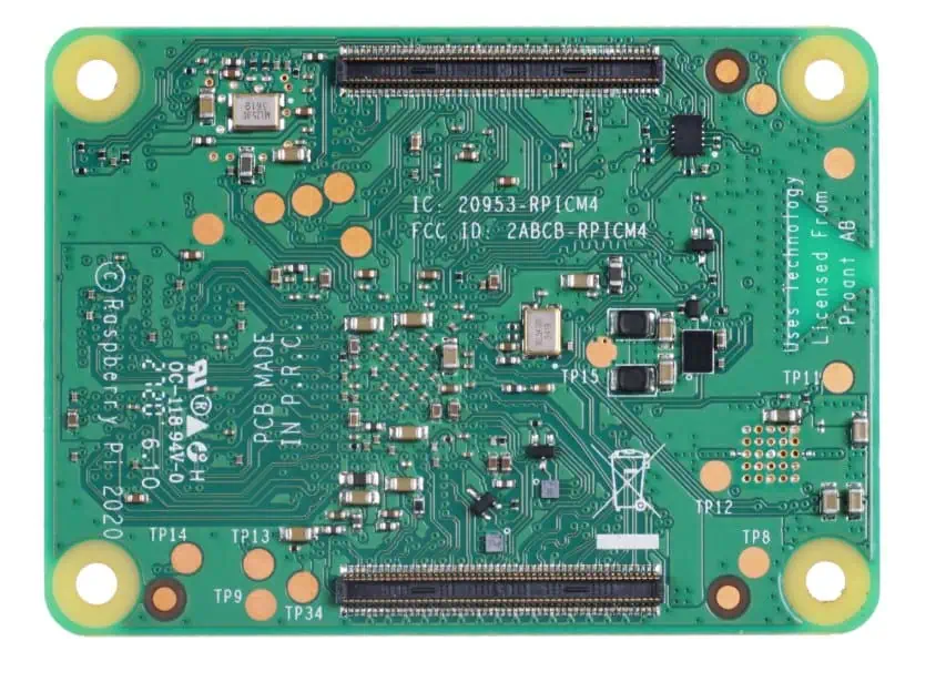
Definition of UL Marking on PCBs

UL marking on a PCB is a visual indicator that the board has been tested and certified to meet specific UL safety standards. This marking typically includes the UL logo, a unique identifier, and sometimes additional information about the certification.

Components of UL Marking

A typical UL mark on a PCB includes:

  1. The UL logo
  2. A unique file number (E-number)
  3. The board’s flame rating
  4. Additional identifiers for specific standards met

Types of UL Marks for PCBs

There are several types of UL marks that can appear on PCBs:

  1. UL Recognized Component Mark: This is the most common for PCBs. It indicates that the PCB is a component intended for use in a complete product, which will undergo its own UL evaluation.
  2. UL Listed Mark: Less common for PCBs alone, this mark is typically found on complete products that have been tested and found to meet UL’s published and nationally recognized standards for safety.
  3. UL Classification Mark: This mark appears on products that UL has evaluated with respect to specific properties, a limited range of hazards, or suitability for use under limited or special conditions.

The Process of Obtaining UL Certification for PCBs

Step 1: Preparation

Before applying for UL certification, manufacturers must ensure their PCBs meet the necessary requirements. This involves:

  1. Designing the PCB to meet UL standards
  2. Selecting materials that comply with UL specifications
  3. Implementing quality control measures in the manufacturing process

Step 2: Application

The manufacturer submits an application to UL, which includes:

  1. Detailed product information
  2. Technical documentation
  3. Samples for testing

Step 3: Product Investigation

UL conducts a thorough investigation of the PCB, which may include:

  1. Physical examination
  2. Performance testing
  3. Flammability testing
  4. Electrical safety testing

Step 4: Report and Follow-up Procedures

If the PCB passes all tests, UL issues a report and establishes follow-up procedures to ensure ongoing compliance. This typically involves:

  1. Regular factory inspections
  2. Periodic retesting of products
  3. Documentation of any changes to the product or manufacturing process

Step 5: Authorization to Apply UL Mark

Once all requirements are met, the manufacturer is authorized to apply the UL mark to their PCBs.

UL Standards Relevant to PCBs

Several UL standards are particularly relevant to PCBs:

UL 94: Standard for Safety of Flammability of Plastic Materials for Parts in Devices and Appliances

This standard is crucial for PCBs as it determines the flammability rating of the board. Common ratings include:

  • V-0: Highest flame-resistant rating
  • V-1: Second highest flame-resistant rating
  • V-2: Third highest flame-resistant rating
  • HB: Horizontal burning test

UL 796: Standard for Printed-Wiring Boards

This standard specifically addresses the safety requirements for PCBs. It covers aspects such as:

  1. Electrical properties
  2. Mechanical strength
  3. Thermal stability
  4. Resistance to chemicals and solvents

UL 746E: Standard for Polymeric Materials – Industrial Laminates, Filament Wound Tubing, Vulcanized Fibre, and Materials Used in Printed-Wiring Boards

This standard focuses on the materials used in PCB manufacturing, ensuring they meet safety and performance requirements.

The Importance of UL Marking on PCBs

1. Safety Assurance

UL marking provides assurance that the PCB has been rigorously tested and meets established safety standards. This is crucial in preventing electrical fires, shocks, and other hazards.

2. Regulatory Compliance

Many countries and industries require UL certification for electronic products. Having UL-marked PCBs can help manufacturers meet these regulatory requirements more easily.

3. Market Access

UL certification can open doors to new markets, particularly in regions where UL standards are widely recognized and respected.

4. Quality Indicator

UL marking serves as an indicator of quality, demonstrating that the PCB manufacturer adheres to high standards in their production processes.

5. Liability Protection

Using UL-certified components can provide a degree of liability protection for manufacturers in case of product-related incidents.

6. Customer Confidence

Many customers, especially in industries like aerospace, medical devices, and telecommunications, specifically require UL-certified components, including PCBs.

Impact of UL Marking on PCB Manufacturing

UL marking has a significant impact on PCB manufacturing processes and industry practices:

1. Material Selection

Manufacturers must carefully select materials that meet UL standards, which can influence costs and availability.

2. Design Considerations

PCB designers need to consider UL requirements when creating board layouts and selecting components.

3. Manufacturing Processes

UL certification often requires specific manufacturing processes and quality control measures to be in place.

4. Documentation and Traceability

Manufacturers must maintain detailed records of materials, processes, and testing to comply with UL requirements.

5. Ongoing Compliance

Regular inspections and testing are necessary to maintain UL certification, requiring ongoing investment from manufacturers.

Challenges in Obtaining and Maintaining UL Certification for PCBs

While UL certification offers numerous benefits, it also presents challenges for PCB manufacturers:

1. Cost

The process of obtaining and maintaining UL certification can be expensive, including fees for testing, inspections, and ongoing compliance.

2. Time

Initial certification can be time-consuming, potentially delaying product launches or updates.

3. Technical Requirements

Meeting UL standards often requires advanced technical knowledge and may necessitate changes to existing designs or processes.

4. Material Limitations

UL certification may limit the materials that can be used in PCB manufacturing, potentially affecting performance or cost.

5. Keeping Up with Changes

UL standards are periodically updated, requiring manufacturers to stay informed and adapt their processes accordingly.

Future Trends in UL Certification for PCBs

As technology evolves, so do the standards and processes for UL certification. Some emerging trends include:

1. Increased Focus on Environmental Sustainability

UL is placing greater emphasis on environmental factors, including the use of sustainable materials and manufacturing processes.

2. Adaptation to New Technologies

As new PCB technologies emerge, such as flexible and 3D-printed PCBs, UL standards are evolving to address their unique characteristics.

3. Enhanced Testing for EMC and Signal Integrity

With the increasing complexity of electronic devices, UL is expanding its focus to include more comprehensive testing for electromagnetic compatibility (EMC) and signal integrity.

4. Integration with IoT and Smart Devices

As PCBs become integral components in Internet of Things (IoT) devices, UL is developing new standards to address the unique safety and security challenges these technologies present.

5. Streamlined Certification Processes

UL is working on ways to make the certification process more efficient, potentially reducing time and costs for manufacturers.

Comparison of UL Certification with Other Standards

While UL certification is widely recognized, it’s not the only standard in the electronics industry. Here’s a comparison of UL with other major standards:

AspectULCECSATรœV
Geographic FocusGlobal (US-based)European UnionCanadaGlobal (German-based)
Type of StandardSafetySafety, Health, EnvironmentalSafetySafety, Quality
RecognitionHigh in North AmericaRequired in EUHigh in CanadaHigh in Europe
ScopeProduct-specificBroad product categoriesProduct-specificProduct and process
Self-DeclarationNoYes (for some products)NoNo
Third-Party TestingRequiredOften requiredRequiredRequired

Conclusion

UL marking on PCBs is more than just a symbol โ€“ it represents a commitment to safety, quality, and reliability in electronics manufacturing. While obtaining and maintaining UL certification presents challenges, the benefits in terms of market access, customer confidence, and safety assurance make it a valuable investment for many PCB manufacturers.

As the electronics industry continues to evolve, UL certification will likely adapt to address new technologies and challenges. PCB manufacturers who stay informed about these changes and maintain their UL certification will be well-positioned to meet the growing demand for safe, high-quality electronic components in an increasingly connected world.

Frequently Asked Questions (FAQ)

  1. Q: Is UL certification mandatory for all PCBs? A: UL certification is not legally mandatory for all PCBs, but it is often required by customers, especially in industries with strict safety regulations. Many countries and industries consider UL certification as a de facto requirement for electronic components.
  2. Q: How long does the UL certification process take for PCBs? A: The duration of the UL certification process can vary significantly depending on factors such as the complexity of the PCB, the readiness of the manufacturer, and the current workload of UL. Typically, it can take anywhere from a few months to a year to complete the initial certification process.
  3. Q: Can a PCB lose its UL certification? A: Yes, a PCB can lose its UL certification if it fails to meet the ongoing requirements. This can happen if the manufacturer changes the design or materials without approval, fails follow-up inspections, or if new standards are introduced that the PCB no longer meets.
  4. Q: How often do UL standards for PCBs change? A: UL standards are reviewed and updated periodically to keep pace with technological advancements and new safety concerns. Major revisions typically occur every 3-5 years, but minor updates can happen more frequently. Manufacturers need to stay informed about these changes to maintain their certification.
  5. Q: Is UL certification recognized worldwide? A: While UL is based in the United States and is most widely recognized in North America, it has global recognition and acceptance in many countries. However, some regions may have their own preferred certification bodies, such as CE marking in the European Union or CCC in China. In many cases, UL certification can help facilitate obtaining these other certifications.

What is Inner Layer Pad Insulation?

Inner layer pad insulation is a crucial component in the construction of printed circuit boards (PCBs), playing a vital role in the overall performance and reliability of electronic devices. This specialized material is designed to provide electrical insulation, thermal management, and structural support within the complex layered structure of multilayer PCBs.

As electronic devices continue to shrink in size while simultaneously increasing in functionality and power, the importance of effective insulation between conductive layers becomes paramount. Inner layer pad insulation addresses this need by creating a barrier between copper layers, preventing short circuits and ensuring the proper functioning of the circuit.

In this comprehensive article, we will explore the various aspects of inner layer pad insulation, including its composition, manufacturing processes, properties, applications, and impact on PCB performance. We will also discuss the latest developments in this field and how they are shaping the future of electronics.

Composition and Types of Inner Layer Pad Insulation

Basic Components

Inner layer pad insulation materials are typically composed of a combination of the following elements:

  1. Base material: Usually a type of polymer or resin
  2. Reinforcing fibers: Glass fibers or other strengthening materials
  3. Flame retardants: Additives to improve fire resistance
  4. Fillers: Materials to enhance specific properties such as thermal conductivity or dimensional stability

Common Types of Inner Layer Pad Insulation

There are several types of materials used for inner layer pad insulation in PCBs. The choice of material depends on various factors, including the specific application, performance requirements, and cost considerations. Here are some of the most common types:

1. FR-4 (Flame Retardant 4)

FR-4 is the most widely used material for PCB substrates and inner layer insulation. It consists of a woven fiberglass cloth impregnated with an epoxy resin system.

Advantages:

  • Good electrical insulation properties
  • Excellent mechanical strength
  • Flame retardant
  • Relatively low cost

Disadvantages:

  • Limited high-frequency performance
  • Moisture absorption can be an issue in some applications

2. Polyimide

Polyimide is a high-performance polymer known for its excellent thermal stability and electrical properties.

Advantages:

  • Exceptional heat resistance
  • Low dielectric constant and loss tangent
  • Good dimensional stability
  • Suitable for flex and rigid-flex applications

Disadvantages:

  • Higher cost compared to FR-4
  • Can be challenging to process

3. PTFE (Polytetrafluoroethylene)

PTFE, also known by the brand name Teflon, is used in high-frequency and high-speed applications.

Advantages:

  • Excellent electrical properties at high frequencies
  • Very low moisture absorption
  • Good chemical resistance

Disadvantages:

  • Expensive
  • Requires specialized processing techniques

4. Ceramic-filled PTFE

This material combines PTFE with ceramic fillers to enhance certain properties.

Advantages:

  • Improved dimensional stability compared to pure PTFE
  • Better thermal conductivity
  • Maintains excellent electrical properties

Disadvantages:

  • Higher cost than standard PTFE
  • Can be brittle and require careful handling

5. BT (Bismaleimide Triazine) Resin

BT resin is an advanced thermoset polymer used in high-performance PCBs.

Advantages:

  • Low dielectric constant and loss tangent
  • Good thermal stability
  • Better dimensional stability than FR-4

Disadvantages:

  • More expensive than FR-4
  • Can be brittle and require careful processing

Manufacturing Process of Inner Layer Pad Insulation

The manufacturing process for inner layer pad insulation is a critical step in PCB production. The process varies depending on the type of material used, but generally follows these steps:

1. Material Preparation

  • Raw materials (resins, reinforcing fibers, additives) are carefully selected and mixed according to the desired formulation.
  • For composite materials like FR-4, fiberglass cloth is prepared in large rolls.

2. Impregnation

  • For materials like FR-4, the fiberglass cloth is passed through a bath of liquid resin.
  • The resin impregnates the cloth, coating the fibers and filling the spaces between them.

3. B-Staging

  • The impregnated material is partially cured in an oven, creating what is known as “prepreg” (pre-impregnated) material.
  • This B-staged material is easier to handle and can be stored for later use.

4. Cutting and Layup

  • The prepreg material is cut to the required size for the PCB.
  • Multiple layers of prepreg are stacked alternately with copper foil layers to create the PCB structure.

5. Lamination

  • The layered stack is placed in a lamination press.
  • Heat and pressure are applied to fully cure the resin and bond all layers together.

6. Drilling and Plating

  • After lamination, holes are drilled through the board for vias and component leads.
  • The holes are then plated with copper to create electrical connections between layers.

7. Etching and Patterning

  • The outer copper layers are etched to create the desired circuit pattern.
  • Inner layer circuits are typically etched before lamination.

8. Final Processing

  • Additional layers such as solder mask and silkscreen are applied.
  • The board undergoes final testing and inspection.

This process creates a multilayer PCB with inner layer pad insulation integrated into its structure. The insulation material provides electrical isolation between conductive layers while also contributing to the overall mechanical and thermal properties of the board.

Properties and Characteristics of Inner Layer Pad Insulation

The effectiveness of inner layer pad insulation is determined by several key properties. These characteristics influence the performance, reliability, and suitability of the PCB for specific applications. Let’s examine the most important properties:

1. Dielectric Constant (Dk)

The dielectric constant, also known as relative permittivity, is a measure of the material’s ability to store electrical energy in an electric field.

  • Lower Dk values generally result in faster signal propagation and less signal loss.
  • Typical Dk values range from about 3.0 to 4.5 for common PCB materials.

2. Dissipation Factor (Df)

Also known as the loss tangent, the dissipation factor indicates the amount of energy lost as heat in the insulation material.

  • Lower Df values result in less signal attenuation and are preferred for high-frequency applications.
  • Common PCB materials have Df values ranging from 0.002 to 0.02.

3. Thermal Conductivity

This property measures the material’s ability to conduct heat.

  • Higher thermal conductivity helps dissipate heat from components and traces.
  • Values typically range from 0.2 to 1.0 W/mยทK for PCB insulation materials.

4. Coefficient of Thermal Expansion (CTE)

CTE describes how the material’s dimensions change with temperature.

  • Matching the CTE of the insulation to that of copper and components helps prevent stress and failure during thermal cycling.
  • CTE is often different in the x-y plane versus the z-axis due to the presence of reinforcing fibers.

5. Glass Transition Temperature (Tg)

Tg is the temperature at which the material transitions from a rigid to a more flexible state.

  • Higher Tg values indicate better performance at elevated temperatures.
  • Common Tg values range from 130ยฐC to over 200ยฐC for high-performance materials.

6. Decomposition Temperature (Td)

Td is the temperature at which the material begins to break down chemically.

  • Higher Td values indicate better resistance to extreme temperatures and processes like lead-free soldering.
  • Td values typically range from 300ยฐC to over 400ยฐC for high-performance materials.

7. Moisture Absorption

This property indicates how much moisture the material absorbs from its environment.

  • Lower moisture absorption is generally preferred to maintain stable electrical and mechanical properties.
  • Values typically range from less than 0.1% to about 0.5% for common PCB materials.

8. Dielectric Strength

Dielectric strength measures the maximum electric field the material can withstand without breaking down.

  • Higher values indicate better insulation properties.
  • Typical values range from 20 to 60 kV/mm for PCB insulation materials.

9. Flexural Strength

This property measures the material’s ability to resist deformation under load.

  • Higher flexural strength indicates better mechanical durability.
  • Values typically range from 300 to 500 MPa for common PCB materials.

To better visualize these properties, let’s look at a comparison table of some common inner layer pad insulation materials:

PropertyFR-4PolyimidePTFEBT Resin
Dielectric Constant (Dk)4.0-4.53.2-3.52.1-2.53.5-3.9
Dissipation Factor (Df)0.015-0.0200.002-0.0050.0002-0.00050.005-0.010
Thermal Conductivity (W/mยทK)0.3-0.50.3-0.50.2-0.30.3-0.4
CTE (ppm/ยฐC) (x-y / z)14-17 / 50-7012-16 / 40-5070-280 / 250-30013-15 / 40-50
Glass Transition Temp (Tg) (ยฐC)130-180250-260N/A180-220
Decomposition Temp (Td) (ยฐC)300-315450-500380-400350-380
Moisture Absorption (%)0.1-0.50.3-0.8<0.010.1-0.3
Dielectric Strength (kV/mm)20-4025-3540-6030-45
Flexural Strength (MPa)300-500350-45010ๆœˆ20ๆ—ฅ300-400

This table illustrates the range of properties available in different inner layer pad insulation materials, highlighting why certain materials are chosen for specific applications based on their unique characteristics.

Applications and Impact on PCB Performance

Inner layer pad insulation plays a crucial role in various PCB applications, significantly impacting the overall performance and reliability of electronic devices. Let’s explore some key applications and how inner layer pad insulation affects PCB performance:

High-Frequency and High-Speed Applications

In applications such as telecommunications, aerospace, and high-performance computing, inner layer pad insulation is critical for maintaining signal integrity.

Impact on Performance:

  • Low Dk and Df materials minimize signal loss and distortion.
  • Controlled impedance is easier to achieve with consistent insulation properties.
  • Reduced crosstalk between adjacent traces due to better insulation.

Power Electronics

Power electronic devices, including power supplies, motor drives, and inverters, rely heavily on effective insulation between high-voltage components.

Impact on Performance:

  • High dielectric strength prevents breakdown under high voltages.
  • Good thermal conductivity helps dissipate heat from power components.
  • Materials with high Tg and Td withstand the higher temperatures associated with power electronics.

Automotive Electronics

The harsh environment and reliability requirements of automotive electronics demand robust insulation materials.

Impact on Performance:

  • Resistance to thermal cycling prevents delamination and cracking.
  • Low moisture absorption maintains consistent performance in varying humidity conditions.
  • Flame retardant properties enhance safety in the event of a vehicle fire.

Aerospace and Defense

These industries require PCBs that can withstand extreme conditions while maintaining high reliability.

Impact on Performance:

  • Materials with low outgassing properties are suitable for space applications.
  • High thermal stability ensures consistent performance across a wide temperature range.
  • Excellent dimensional stability prevents warpage and misalignment in critical systems.

Medical Devices

Medical electronics often require biocompatibility and the ability to withstand sterilization processes.

Impact on Performance:

  • Materials resistant to chemicals used in sterilization processes maintain integrity.
  • Low moisture absorption prevents performance changes in high-humidity environments.
  • Consistent electrical properties ensure reliable operation of sensitive medical equipment.

Internet of Things (IoT) Devices

As IoT devices become smaller and more ubiquitous, the role of inner layer pad insulation becomes increasingly important.

Impact on Performance:

  • Thin, high-performance materials allow for miniaturization without compromising functionality.
  • Low Dk materials support the high-frequency communications often used in IoT devices.
  • Materials with good thermal management properties help dissipate heat in compact designs.

5G and Beyond

The rollout of 5G networks and development of future communication technologies place new demands on PCB materials.

Impact on Performance:

  • Extremely low loss materials are essential for minimizing signal attenuation at millimeter-wave frequencies.
  • Consistent Dk across a wide frequency range ensures predictable performance.
  • Materials with low moisture sensitivity maintain stable performance in outdoor installations.

Recent Developments and Future Trends

The field of inner layer pad insulation is continuously evolving to meet the growing demands of the electronics industry. Here are some recent developments and future trends:

1. Advanced Composite Materials

Researchers and manufacturers are developing new composite materials that combine the benefits of different insulation types.

Example: Hybrid materials that incorporate both ceramic and polymer components to achieve optimal electrical and thermal properties.

2. Nanotechnology-Enhanced Insulation

The integration of nanomaterials into traditional insulation materials is opening up new possibilities for performance enhancement.

Example: Carbon nanotubes or graphene added to epoxy resins to improve thermal conductivity and mechanical strength.

3. Eco-Friendly and Sustainable Materials

There is a growing focus on developing insulation materials that are more environmentally friendly and sustainable.

Example: Bio-based epoxy resins derived from renewable resources, reducing the reliance on petroleum-based products.

4. Ultra-Low Loss Materials

For applications in 5G, 6G, and beyond, there is a push to develop materials with extremely low dielectric loss.

Example: Advanced PTFE composites with Df values below 0.0010 across a wide frequency range.

5. Adaptive and Smart Materials

Research is being conducted on insulation materials that can adapt their properties in response to environmental conditions.

Example: Materials that can change their thermal conductivity based on temperature, improving heat management in variable load conditions.

6. 3D Printable Insulation Materials

As additive manufacturing techniques for electronics advance, there is interest in developing inner layer pad insulation materials suitable for 3D printing.

Example: Specialized resins that can be 3D printed and cured to form complex, multi-material PCB structures.

7. Integration of Functional Properties

Future insulation materials may incorporate additional functionalities beyond traditional electrical and thermal properties.

Example: Insulation layers with built-in EMI shielding or self-healing capabilities to improve long-term reliability.

8. Artificial Intelligence in Material Design

AI and machine learning techniques are being applied to accelerate the development and optimization of new insulation materials.

Example: Using AI to predict material properties and performance, reducing the time and cost of experimental testing.

Conclusion

Inner layer pad insulation is a critical component in the design and manufacture of modern PCBs, playing a vital role in the performance, reliability, and miniaturization of electronic devices. As we’ve explored in this article, the choice of insulation material impacts various aspects of PCB performance, from signal integrity and thermal management to mechanical durability and environmental resistance.

The field of inner layer pad insulation continues to evolve, driven by the demands of emerging technologies such as 5G, IoT, and advanced computing systems. Innovations in material science, nanotechnology, and manufacturing processes are pushing the boundaries of what’s possible in PCB design and performance.

As electronic devices become increasingly integrated into every aspect of our lives, the importance of high-quality, reliable inner layer pad insulation will only grow. Engineers and designers must stay informed about the latest developments in this field to create the next generation of electronic products that are faster, smaller, more efficient, and more reliable than ever before.

What Paste to Be Used on Heat Sink?

Heat management is crucial in modern electronics, and choosing the right thermal paste for your heat sink can make a significant difference in system performance and longevity. This article will explore various types of thermal pastes, their properties, and how to select the best one for your specific needs.

Understanding Thermal Paste and Its Importance

What is Thermal Paste?

Thermal paste, also known as thermal compound, thermal grease, or heat sink paste, is a thermally conductive material applied between a heat source (such as a CPU or GPU) and a heat sink. Its primary purpose is to eliminate air gaps and improve heat transfer between the two surfaces.

Why is Thermal Paste Necessary?

Even seemingly smooth surfaces have microscopic imperfections that can trap air, which is a poor conductor of heat. Thermal paste fills these gaps, ensuring optimal thermal conductivity and efficient heat dissipation.

Types of Thermal Paste

A heatsink on a graphics chip

Metal-Based Thermal Pastes

Metal-based thermal pastes contain small metal particles, typically silver or aluminum, suspended in a carrier fluid.

Advantages:

  • High thermal conductivity
  • Long-lasting performance
  • Suitable for high-performance applications

Disadvantages:

  • Can be electrically conductive
  • Potential for short circuits if not applied carefully
  • Often more expensive than other types

Ceramic-Based Thermal Pastes

Ceramic-based pastes use ceramic particles as the primary heat-conducting material.

Advantages:

  • Non-electrically conductive
  • Safe for most applications
  • Generally more affordable than metal-based pastes

Disadvantages:

  • Lower thermal conductivity compared to metal-based pastes
  • May dry out over time

Carbon-Based Thermal Pastes

Carbon-based thermal pastes utilize carbon particles, often in the form of graphite or diamond particles.

Advantages:

  • High thermal conductivity
  • Non-electrically conductive
  • Often easier to apply and clean up

Disadvantages:

  • Can be more expensive, especially diamond-based pastes
  • May have lower viscosity, making application trickier

Silicone-Based Thermal Pastes

Silicone-based pastes are among the most common and widely used thermal compounds.

Advantages:

  • Good thermal conductivity
  • Easy to apply and remove
  • Non-electrically conductive

Disadvantages:

  • May dry out over time
  • Not as effective as some other types for high-performance applications

Comparing Thermal Paste Performance

To help you understand the differences between various thermal paste types, here’s a comparison table of typical thermal conductivity values:

Thermal Paste TypeTypical Thermal Conductivity (W/mK)
Metal-based5.-12
Ceramic-based3.-8
Carbon-based4.-12
Silicone-based2.-6

Note that these values are approximate and can vary between specific products within each category.

Factors to Consider When Choosing Thermal Paste

Thermal Conductivity

Thermal conductivity is a measure of a material’s ability to conduct heat. Higher values indicate better heat transfer capabilities. When selecting a thermal paste, consider the thermal demands of your system and choose a paste with appropriate thermal conductivity.

Ease of Application

Some thermal pastes are easier to apply than others. Consider your experience level and the frequency with which you’ll be applying the paste. For beginners or infrequent users, a paste with good viscosity and easy application properties may be preferable.

Electrical Conductivity

If you’re working with sensitive electronic components, it’s crucial to choose a non-electrically conductive thermal paste to prevent short circuits and component damage.

Longevity and Curing Time

Some thermal pastes require a curing period to reach optimal performance, while others work immediately. Consider how long the paste will maintain its effectiveness and whether it needs to be replaced periodically.

Price and Value

While high-end thermal pastes can offer superior performance, they may not be necessary for all applications. Balance your budget with your performance needs to find the best value for your specific use case.

Application Techniques

The Pea Method

  1. Clean both the heat sink and CPU surfaces with isopropyl alcohol.
  2. Apply a small, pea-sized dot of thermal paste to the center of the CPU.
  3. Install the heat sink, allowing the pressure to spread the paste evenly.

The Spread Method

  1. Clean both surfaces thoroughly.
  2. Apply a small amount of paste to the CPU surface.
  3. Use a plastic card or spatula to spread the paste evenly across the entire surface.
  4. Install the heat sink.

The Line Method

  1. Clean both surfaces.
  2. Apply a thin line of paste across the center of the CPU.
  3. Install the heat sink, allowing the pressure to spread the paste.

Common Mistakes to Avoid

Using Too Much Paste

Contrary to popular belief, more thermal paste doesn’t equal better heat transfer. Excess paste can actually impede heat dissipation and make cleanup difficult.

Neglecting to Clean Surfaces

Failing to properly clean the CPU and heat sink surfaces before applying new thermal paste can significantly reduce its effectiveness.

Trapping Air Bubbles

When applying the paste, be careful not to introduce air bubbles, as they can reduce thermal conductivity.

Ignoring Manufacturer Recommendations

Some CPUs or GPUs may have specific requirements or recommendations for thermal paste application. Always consult your hardware’s documentation.

Maintaining and Replacing Thermal Paste

When to Replace Thermal Paste

  • Every 1-2 years for optimal performance
  • If you notice higher than usual temperatures
  • When removing and reinstalling the heat sink

Signs of Degraded Thermal Paste

  • Increased CPU or GPU temperatures under load
  • Thermal throttling or unexpected performance drops
  • Visual inspection reveals dried or cracked paste

Specialized Thermal Solutions

Liquid Metal Thermal Compounds

Liquid metal compounds, typically made of gallium alloys, offer extremely high thermal conductivity.

Advantages:

  • Exceptional thermal performance
  • Long-lasting

Disadvantages:

  • Electrically conductive
  • Can be corrosive to certain metals
  • Difficult to apply and clean up

Thermal Pads

Thermal pads are pre-formed sheets of thermally conductive material that can be cut to size.

Advantages:

  • Easy to apply
  • No risk of spills or mess
  • Reusable in some cases

Disadvantages:

  • Generally lower thermal conductivity than pastes
  • May not conform as well to surface irregularities

Environmental and Safety Considerations

Toxicity and Handling

Some thermal pastes may contain toxic materials. Always read and follow the manufacturer’s safety guidelines and use appropriate personal protective equipment when handling thermal compounds.

Disposal

Dispose of used thermal paste and cleaning materials according to local regulations. Some thermal compounds may be considered hazardous waste.

Conclusion

Choosing the right thermal paste for your heat sink is crucial for maintaining optimal system performance and longevity. Consider factors such as thermal conductivity, ease of application, and compatibility with your specific hardware when making your selection. By understanding the different types of thermal pastes available and following proper application techniques, you can ensure efficient heat dissipation and protect your valuable components.

FAQ

Q1: How often should I replace my thermal paste?

A1: Generally, it’s recommended to replace thermal paste every 1-2 years for optimal performance. However, if you notice higher than usual temperatures or if you remove the heat sink for any reason, it’s a good idea to reapply fresh thermal paste.

Q2: Can I use toothpaste as a substitute for thermal paste?

A2: While toothpaste may work as a very short-term emergency solution, it’s not recommended for regular use. Toothpaste is not designed for heat transfer and can dry out quickly, potentially damaging your components. Always use proper thermal paste designed for electronics.

Q3: Is expensive thermal paste always better than cheaper options?

A3: Not necessarily. While some high-end thermal pastes offer superior performance, many mid-range options provide excellent results for most users. The best choice depends on your specific needs and hardware. For typical consumer applications, a good quality, mid-range thermal paste is often sufficient.

Q4: Can I mix different types of thermal paste?

A4: It’s not recommended to mix different types of thermal paste. Different formulations may react unpredictably when combined, potentially reducing effectiveness or even damaging components. Always clean off old paste completely before applying a new compound.

Q5: Is it necessary to let thermal paste cure before using my computer?

A5: It depends on the specific thermal paste you’re using. Some pastes work optimally right away, while others may require a curing period. Always check the manufacturer’s instructions for your particular thermal paste. If a curing period is recommended, it typically involves running the system under load for a specified time to allow the paste to settle and achieve its best performance.

What is the galvanic process of electrolysis?

The galvanic process of electrolysis is a fundamental electrochemical technique that has revolutionized various industries, from metal refining to water treatment. This process harnesses the power of electricity to drive non-spontaneous chemical reactions, allowing for the separation, purification, and production of various materials. In this comprehensive article, we will explore the principles behind the galvanic process of electrolysis, its applications, and its significance in modern technology and industry.

Understanding Electrolysis

Definition of Electrolysis

Electrolysis is an electrochemical process in which electrical energy is used to drive a non-spontaneous chemical reaction. This process involves the decomposition of a compound in a liquid state or in solution by passing an electric current through it.

Key Components of an Electrolytic Cell

To understand the galvanic process of electrolysis, it’s essential to familiarize ourselves with the key components of an electrolytic cell:

  1. Electrolyte: A solution or molten substance that conducts electricity through the movement of ions.
  2. Electrodes: Conductors that provide the path for electrons to enter or leave the electrolyte.
    • Anode: The positive electrode where oxidation occurs.
    • Cathode: The negative electrode where reduction occurs.
  3. Power source: Provides the electrical energy needed to drive the non-spontaneous reaction.
  4. Container: Holds the electrolyte and electrodes.

The Galvanic Process of Electrolysis

Principles of the Galvanic Process

The galvanic process of electrolysis is based on the principles of electrochemistry and involves the following key concepts:

  1. Oxidation-Reduction (Redox) Reactions
  2. Faraday’s Laws of Electrolysis
  3. Electrode Potentials
  4. Ion Migration

Steps in the Galvanic Process of Electrolysis

The galvanic process of electrolysis typically involves the following steps:

  1. Preparation of the electrolyte
  2. Setup of the electrolytic cell
  3. Application of electrical current
  4. Ion migration and electrode reactions
  5. Product formation and collection

Let’s explore each of these steps in more detail.

1. Preparation of the Electrolyte

The first step in the galvanic process of electrolysis is to prepare the electrolyte. This involves:

  • Selecting an appropriate compound or solution
  • Ensuring the electrolyte is in a conductive state (molten or dissolved in a solvent)
  • Adjusting the concentration if necessary

2. Setup of the Electrolytic Cell

Once the electrolyte is prepared, the electrolytic cell is set up:

  • The electrolyte is placed in a suitable container
  • Electrodes (anode and cathode) are positioned in the electrolyte
  • The electrodes are connected to a power source

3. Application of Electrical Current

With the cell set up, an electrical current is applied:

  • The power source provides a direct current (DC)
  • The current flows from the negative terminal of the power source to the cathode
  • Electrons flow through the external circuit from the anode to the cathode

4. Ion Migration and Electrode Reactions

As the current flows, ion migration and electrode reactions occur:

  • Positively charged ions (cations) migrate towards the cathode
  • Negatively charged ions (anions) migrate towards the anode
  • Oxidation occurs at the anode, releasing electrons
  • Reduction occurs at the cathode, consuming electrons

5. Product Formation and Collection

The final step involves the formation and collection of products:

  • Reduced species form at the cathode
  • Oxidized species form at the anode
  • Gaseous products may be collected
  • Solid products may be deposited on the electrodes or collected from the electrolyte

Faraday’s Laws of Electrolysis

Faraday’s Laws of Electrolysis are fundamental principles that govern the quantitative aspects of electrolysis:

First Law of Faraday

The mass of a substance produced at an electrode during electrolysis is directly proportional to the quantity of electricity passed through the electrolyte.

Second Law of Faraday

The masses of different substances produced by the same quantity of electricity are proportional to their chemical equivalent weights.

These laws can be summarized in the following equation:

m = (Q ร— M) / (n ร— F)

Where:

  • m = mass of the substance produced (in grams)
  • Q = total electric charge passed through the substance (in coulombs)
  • M = molar mass of the substance (in grams per mole)
  • n = number of electrons transferred per ion
  • F = Faraday constant (96,485 coulombs per mole)

Applications of the Galvanic Process of Electrolysis

The galvanic process of electrolysis has numerous applications across various industries:

1. Metal Refining and Production

Electrolysis is widely used in the production and purification of metals:

  • Aluminum production from bauxite ore
  • Copper refining
  • Zinc production
  • Magnesium extraction from seawater

2. Electroplating

Electroplating is a process that uses electrolysis to coat one metal with another:

3. Water Treatment

Electrolysis plays a crucial role in various water treatment processes:

  • Desalination of seawater
  • Removal of heavy metals from wastewater
  • Disinfection of drinking water
  • Generation of hydrogen and oxygen through water electrolysis

4. Chemical Production

Many important chemicals are produced through electrolysis:

  • Chlorine and sodium hydroxide production (chlor-alkali process)
  • Hydrogen and oxygen production
  • Potassium perchlorate synthesis
  • Adiponitrile production for nylon manufacturing

5. Energy Storage

Electrolysis is essential in some energy storage technologies:

  • Hydrogen production for fuel cells
  • Charging of rechargeable batteries
  • Flow batteries for grid-scale energy storage

Comparison of Different Electrolytic Processes

To better understand the galvanic process of electrolysis, it’s helpful to compare it with other electrolytic processes:

ProcessElectrolyteElectrodesProductsApplications
Galvanic ElectrolysisAqueous or molten ionic compoundInert or active electrodesVaries based on electrolyteMetal refining, electroplating, chemical production
Electrochemical MachiningSalt solutionWorkpiece (anode) and tool (cathode)Shaped metal workpiecePrecision metal shaping
ElectropolishingAcid solutionWorkpiece (anode) and cathodeSmooth metal surfaceMetal finishing, medical device manufacturing
AnodizingAcid solutionAluminum (anode) and cathodeOxide layer on aluminumCorrosion resistance, decorative finishes
ElectrodialysisSalt solutionIon-selective membranes

Advantages and Limitations of the Galvanic Process of Electrolysis

Advantages

  1. High purity: Can produce extremely pure materials
  2. Precision: Allows for precise control of reaction rates and products
  3. Versatility: Applicable to a wide range of materials and processes
  4. Environmentally friendly: Can be used for pollution control and clean energy production
  5. Energy efficiency: Direct conversion of electrical energy to chemical energy

Limitations

  1. Energy consumption: Requires a continuous supply of electrical energy
  2. Cost: Initial setup and ongoing energy costs can be high
  3. Scale limitations: Some processes are challenging to scale up
  4. Material constraints: Not all materials are suitable for electrolysis
  5. Safety concerns: Potential risks associated with handling strong electrolytes and electrical currents

Future Trends and Innovations

The galvanic process of electrolysis continues to evolve, with several promising trends and innovations on the horizon:

  1. Advanced electrode materials: Development of more efficient and durable electrode materials
  2. Nanostructured electrocatalysts: Enhancing reaction rates and selectivity
  3. Renewable energy integration: Coupling electrolysis with solar and wind power for green hydrogen production
  4. Microfluidic electrolysis: Miniaturization of electrolytic processes for lab-on-a-chip applications
  5. Bioelectrolysis: Using microorganisms to enhance electrolytic processes
  6. Solid-state electrolytes: Development of new materials for safer and more efficient electrolysis

Conclusion

The galvanic process of electrolysis is a powerful and versatile technique that has found applications in numerous industries and technologies. By harnessing the power of electricity to drive chemical reactions, electrolysis enables the production of pure materials, the treatment of water, and the storage of energy. As we continue to face global challenges in energy, environmental protection, and resource management, the importance of electrolysis is likely to grow. With ongoing research and innovation, we can expect to see even more efficient and sustainable applications of this fundamental electrochemical process in the future.

Frequently Asked Questions (FAQ)

1. How does the galvanic process of electrolysis differ from a galvanic cell?

The galvanic process of electrolysis and a galvanic cell are related but distinct electrochemical systems:

Galvanic Process of Electrolysis:

  • Requires external electrical energy
  • Drives non-spontaneous reactions
  • Used for chemical decomposition or synthesis
  • Converts electrical energy to chemical energy

Galvanic Cell:

  • Produces electrical energy
  • Involves spontaneous redox reactions
  • Used in batteries and fuel cells
  • Converts chemical energy to electrical energy

In essence, electrolysis is the reverse process of what occurs in a galvanic cell. While a galvanic cell harnesses spontaneous chemical reactions to generate electricity, electrolysis uses electricity to force non-spontaneous chemical reactions to occur.

2. What factors affect the efficiency of the galvanic process of electrolysis?

Several factors can influence the efficiency of electrolysis:

  1. Electrode material: Different materials have varying overpotentials and catalytic properties.
  2. Electrolyte concentration: Affects conductivity and ion availability.
  3. Temperature: Higher temperatures generally increase reaction rates and conductivity.
  4. Current density: Higher current densities can increase reaction rates but may reduce efficiency.
  5. Cell design: Proper electrode spacing and electrolyte circulation can improve efficiency.
  6. Presence of impurities: Can interfere with desired reactions or cause side reactions.
  7. pH of the electrolyte: Affects the ease of certain reactions and product formation.
  8. Applied voltage: Must be sufficient to overcome the thermodynamic and kinetic barriers of the reaction.

Optimizing these factors can significantly improve the efficiency and selectivity of the electrolytic process.

3. Can the galvanic process of electrolysis be used for environmental remediation?

Yes, the galvanic process of electrolysis has several applications in environmental remediation:

  1. Water treatment:
    • Removal of heavy metals from wastewater
    • Destruction of organic pollutants
    • Desalination of brackish water or seawater
  2. Soil remediation:
    • Electrokinetic removal of heavy metals from contaminated soils
    • Degradation of organic pollutants in soil
  3. Air purification:
    • Electrostatic precipitation of particulates
    • Ozone generation for air disinfection
  4. Carbon dioxide reduction:
    • Electrochemical conversion of CO2 to valuable chemicals or fuels

These applications demonstrate the potential of electrolysis in addressing various environmental challenges, from water pollution to greenhouse gas reduction.

4. How does the choice of electrode material affect the galvanic process of electrolysis?

The choice of electrode material is crucial in the galvanic process of electrolysis and can significantly impact the process efficiency and products formed:

  1. Reactivity: Some electrodes (like platinum) are inert, while others (like copper) may participate in the reaction.
  2. Overpotential: Different materials have varying overpotentials, affecting the energy required for the reaction.
  3. Catalytic activity: Some materials catalyze specific reactions, improving efficiency and selectivity.
  4. Durability: Electrodes must withstand the corrosive environment of the electrolyte.
  5. Conductivity: Higher conductivity reduces energy losses.
  6. Cost: Some materials (like platinum) are expensive but highly effective.

Common electrode materials include:

  • Platinum: Excellent catalytic properties, inert, expensive
  • Graphite: Inexpensive, good for chlor-alkali process
  • Lead dioxide: Used in lead-acid batteries
  • Dimensionally Stable Anodes (DSA): Titanium coated with metal oxides, used in chlorine production

The choice of electrode material depends on the specific requirements of the electrolytic process, balancing factors like efficiency, cost, and durability.

5. What are the safety considerations when performing the galvanic process of electrolysis?

Safety is paramount when conducting electrolysis. Key considerations include:

  1. Electrical safety:
    • Use properly insulated equipment
    • Ensure proper grounding
    • Use low-voltage DC power supplies when possible
  2. Chemical hazards:
    • Handle corrosive electrolytes with care
    • Be aware of potentially toxic or flammable products
    • Use appropriate personal protective equipment (PPE)
  3. Gas evolution:
    • Ensure proper ventilation to prevent accumulation of potentially explosive gases
    • Use gas sensors if working with dangerous gases
  4. Heat generation:
    • Be aware of heat produced during electrolysis
    • Use cooling systems if necessary
  5. Pressure buildup:
    • Design cells to safely release any pressure buildup
    • Use pressure relief valves when necessary
  6. Material compatibility:
    • Ensure all materials are compatible with the electrolyte and expected products
  7. Training:
    • Ensure all operators are properly trained in electrolysis procedures and safety protocols
  8. Emergency procedures:
    • Have clear emergency shutdown procedures
    • Keep appropriate fire extinguishers and first aid equipment readily available

By adhering to these safety considerations, the risks associated with the galvanic process of electrolysis can be minimized, ensuring a safe working environment.

How Often Can You Raise a PCB to Lead-free Soldering Temperatures?

In the world of electronics manufacturing, the transition to lead-free soldering has brought about numerous challenges and considerations. One of the most critical aspects of this shift is the impact of higher soldering temperatures on printed circuit boards (PCBs) and their components. As lead-free solders typically require higher melting points compared to traditional lead-based solders, the question of how often a PCB can be exposed to these elevated temperatures has become increasingly important.

This comprehensive article will explore the factors influencing the thermal resilience of PCBs, the effects of repeated exposure to lead-free soldering temperatures, and best practices for managing thermal stress in PCB assembly and rework processes. By understanding these aspects, manufacturers can optimize their processes to ensure the reliability and longevity of their electronic products.

Understanding Lead-free Soldering Temperatures

The Shift to Lead-free Soldering

The global electronics industry has been moving away from lead-based solders due to environmental and health concerns. This transition has necessitated the use of alternative solder alloys, most of which require higher processing temperatures.

Typical Lead-free Soldering Temperatures

Lead-free solders generally have higher melting points compared to traditional tin-lead solders. Here’s a comparison of common solder alloys and their melting points:

Solder TypeCompositionMelting Point (ยฐC)
Tin-Lead (SnPb)63% Sn, 37% Pb183
SAC305 (Lead-free)96.5% Sn, 3% Ag, 0.5% Cu217-220
SAC405 (Lead-free)95.5% Sn, 4% Ag, 0.5% Cu217-220
SN100C (Lead-free)99.3% Sn, 0.7% Cu, Ni, Ge227

As evident from the table, lead-free solders typically require temperatures 30-40ยฐC higher than traditional lead-based solders during the reflow process.

Factors Affecting PCB Thermal Resilience

Several factors influence how well a PCB can withstand repeated exposure to lead-free soldering temperatures:

1. PCB Material Properties

Glass Transition Temperature (Tg)

The glass transition temperature (Tg) is a critical property of PCB materials. It represents the temperature at which the material begins to soften and transition from a rigid to a more pliable state.

PCB MaterialTypical Tg Range (ยฐC)
FR-4 (Standard)130-140
High-Tg FR-4170-180
Polyimide>250

PCBs with higher Tg values generally exhibit better resistance to thermal stress and can withstand more reflow cycles.

Coefficient of Thermal Expansion (CTE)

The CTE describes how much a material expands or contracts with temperature changes. Mismatches in CTE between different PCB materials and components can lead to stress and potential failure during thermal cycling.

2. PCB Design and Construction

Layer Count and Thickness

Thicker, multi-layer PCBs generally have better thermal distribution and can withstand more reflow cycles compared to thinner, single-layer boards.

Copper Distribution

Even distribution of copper across the PCB layers helps in uniform heat distribution, reducing the risk of localized thermal stress.

Via Design

Proper via design, including the use of thermal relief vias, can help manage heat dissipation during the soldering process.

3. Component Properties

Component Thermal Sensitivity

Different components have varying levels of thermal sensitivity. For example, electrolytic capacitors are generally more sensitive to high temperatures compared to ceramic capacitors.

Package Type

The type of component package (e.g., BGA, QFP, SMD) can affect its ability to withstand repeated thermal cycles.

4. Soldering Process Parameters

Peak Temperature

The maximum temperature reached during the reflow process significantly impacts the thermal stress on the PCB and components.

Time Above Liquidus (TAL)

The duration for which the PCB is exposed to temperatures above the solder’s melting point affects the cumulative thermal stress.

Heating and Cooling Rates

Rapid temperature changes can induce thermal shock, potentially leading to PCB or component damage.

Effects of Repeated Exposure to Lead-free Soldering Temperatures

Subjecting a PCB to multiple lead-free soldering cycles can have various effects on its integrity and reliability:

1. PCB Delamination

Repeated thermal stress can cause separation between the layers of a multi-layer PCB, leading to delamination.

2. Pad Cratering

High temperatures and thermal cycling can cause microcracks in the resin between copper pads and the PCB substrate.

3. Component Damage

Sensitive components may suffer internal damage or degradation due to repeated exposure to high temperatures.

4. Solder Joint Reliability

Multiple reflow cycles can affect the reliability of solder joints, potentially leading to weak or brittle connections.

5. Warpage

PCB warpage can occur due to CTE mismatches and cumulative thermal stress, affecting component placement and overall board functionality.

Guidelines for Multiple Reflow Cycles

While the exact number of times a PCB can be safely exposed to lead-free soldering temperatures varies depending on the factors mentioned earlier, here are some general guidelines:

Standard FR-4 PCBs

For typical FR-4 PCBs, it’s generally recommended to limit the number of reflow cycles to 3-5 times.

High-Tg FR-4 PCBs

High-Tg FR-4 boards may withstand 5-7 reflow cycles, depending on the specific material properties and design.

Polyimide PCBs

Polyimide PCBs, due to their higher temperature resistance, can potentially undergo 7-10 reflow cycles.

It’s important to note that these are general guidelines, and actual limits should be determined through testing and validation for specific PCB designs and applications.

Best Practices for Managing Thermal Stress

To maximize the number of times a PCB can be safely exposed to lead-free soldering temperatures, consider the following best practices:

1. Material Selection

Choose PCB materials with appropriate Tg values and thermal properties for your application.

2. Thermal Profiling

Develop and optimize reflow profiles to minimize thermal stress while ensuring proper solder joint formation.

3. Component Placement

Consider the thermal sensitivity of components when designing the PCB layout.

4. Use of Thermal Relief Pads

Implement thermal relief pads to manage heat distribution and reduce thermal stress on sensitive components.

5. Preheating and Controlled Cooling

Incorporate gradual preheating and controlled cooling stages in the reflow profile to minimize thermal shock.

6. Nitrogen Atmosphere

Consider using a nitrogen atmosphere during reflow, which can allow for lower peak temperatures and shorter TAL.

7. Rework Strategies

Develop strategies to minimize the number of rework cycles required, such as using selective soldering techniques for repairs.

8. Thermal Simulation

Utilize thermal simulation tools to predict and optimize heat distribution across the PCB during the reflow process.

Monitoring and Testing

To ensure PCB reliability after multiple lead-free soldering cycles, implement the following monitoring and testing procedures:

1. X-ray Inspection

Use X-ray inspection to detect internal defects such as voids or cracks that may develop after multiple reflow cycles.

2. Thermal Cycling Tests

Conduct thermal cycling tests to evaluate the long-term reliability of PCBs and components after repeated exposure to high temperatures.

3. Cross-sectioning Analysis

Perform cross-sectioning analysis to examine the internal structure of PCBs and solder joints for signs of degradation.

4. Electrical Testing

Implement comprehensive electrical testing to ensure functionality and performance after each reflow cycle.

5. Warpage Measurement

Use warpage measurement techniques to assess the cumulative effects of thermal stress on PCB flatness.

Conclusion

lead free solder

The question of how often a PCB can be raised to lead-free soldering temperatures does not have a one-size-fits-all answer. It depends on a complex interplay of factors including PCB material properties, design considerations, component characteristics, and process parameters. While general guidelines suggest limiting reflow cycles to 3-10 times depending on the PCB material, the actual limit for a specific design should be determined through careful testing and validation.

By understanding the factors affecting PCB thermal resilience, implementing best practices for managing thermal stress, and utilizing appropriate monitoring and testing procedures, manufacturers can optimize their processes to maximize PCB reliability while meeting the challenges of lead-free soldering. As the electronics industry continues to evolve, ongoing research and development in PCB materials and manufacturing techniques will likely lead to further improvements in thermal resilience and reliability.

Frequently Asked Questions (FAQ)

1. Can I use the same reflow profile for all lead-free PCB assemblies?

While a general lead-free reflow profile can serve as a starting point, it’s not recommended to use the exact same profile for all PCB assemblies. Each PCB design may require a tailored reflow profile due to variations in:

  • Board thickness and layer count
  • Component mix and thermal mass
  • Solder paste composition
  • PCB material properties

It’s best practice to develop and optimize a specific reflow profile for each PCB design, considering factors such as:

  • Ramp rates (heating and cooling)
  • Soak times and temperatures
  • Peak temperature and time above liquidus
  • Overall thermal budget

Using thermal profiling equipment and software can help in developing and fine-tuning reflow profiles for specific PCB assemblies, ensuring optimal solder joint formation while minimizing thermal stress on the board and components.

2. How does the use of mixed technology (through-hole and SMT components) affect the number of allowable reflow cycles?

The use of mixed technology on a PCB can complicate the reflow process and potentially limit the number of allowable reflow cycles. This is due to several factors:

  1. Thermal mass differences: Through-hole components typically have higher thermal mass than SMT components, leading to uneven heating and cooling across the board.
  2. Heat exposure for through-hole components: When SMT components are reflowed, through-hole components are also exposed to high temperatures, potentially exceeding their rated limits.
  3. Stress on plated through-holes: Repeated thermal cycling can cause stress on plated through-holes, potentially leading to barrel cracks or pad lifting.
  4. Flux residues: Multiple reflow cycles can lead to accumulation of flux residues, particularly in through-hole areas, affecting cleanliness and potentially long-term reliability.

To manage these challenges:

  • Consider using a selective soldering process for through-hole components after SMT reflow.
  • Optimize component placement to balance thermal distribution.
  • Use thermally robust PCB materials and design techniques.
  • Implement strict process controls and thermal profiling.

Generally, mixed technology boards may require more conservative limits on the number of reflow cycles compared to pure SMT assemblies. Thorough testing and validation are crucial to determine safe limits for specific designs.

3. What are the signs that a PCB has been exposed to too many reflow cycles?

Several indicators can suggest that a PCB has been subjected to excessive thermal stress from multiple reflow cycles:

  1. Visual indicators:
    • Discoloration or browning of the PCB substrate
    • Measurable warpage or twisting of the board
    • Lifted or separated pads
    • Cracks in the solder mask
  2. Structural issues:
    • Delamination between PCB layers (detectable via microsection analysis or ultrasonic inspection)
    • Barrel cracks in plated through-holes
    • Pad cratering (separation of pads from the laminate)
  3. Solder joint problems:
    • Excessive intermetallic compound (IMC) growth
    • Brittle or cracked solder joints
    • Voiding in solder joints
  4. Component issues:
    • Package deformation or cracking
    • Internal damage to sensitive components (e.g., delamination in MLCCs)
  5. Electrical problems:
    • Intermittent connections
    • Changes in impedance characteristics
    • Increased leakage currents
  6. Performance degradation:
    • Shifts in electrical parameters
    • Reduced reliability or lifespan of the assembly

Regular inspection, both visual and using advanced techniques like X-ray and thermal imaging, can help detect these issues early. If any of these signs are observed, it may indicate that the PCB has reached or exceeded its safe limit for reflow cycles.

4. How does the transition to lead-free soldering affect the rework process for PCBs?

The transition to lead-free soldering has significantly impacted the rework process for PCBs in several ways:

  1. Higher temperatures:
    • Lead-free solders require higher rework temperatures, increasing the risk of thermal damage to PCBs and components.
    • More precise temperature control is necessary during rework.
  2. Narrower process window:
    • The temperature range between solder melting and component damage is smaller, requiring more precise heating methods.
  3. Different solder behavior:
    • Lead-free solders often have poorer wetting characteristics, making rework more challenging.
    • The higher surface tension of lead-free solders can make it harder to remove components.
  4. Component considerations:
    • Some components may not be rated for multiple exposures to lead-free reflow temperatures, limiting rework options.
  5. Equipment and tooling:
    • Rework stations may need upgrading to handle higher temperatures and provide more precise control.
    • Specialized nozzles and tooling may be required for effective lead-free rework.
  6. Increased risk of PCB damage:
    • Higher temperatures increase the risk of pad lifting, delamination, and other thermal damage during rework.
  7. Flux considerations:
    • Different flux formulations may be necessary to work effectively with lead-free solders at higher temperatures.
  8. Inspection and quality control:
    • More rigorous inspection may be required after rework due to the increased risks associated with higher temperatures.

To address these challenges:

  • Develop specific rework profiles for lead-free assemblies.
  • Invest in advanced rework equipment with precise temperature control.
  • Train technicians on lead-free rework techniques.
  • Consider using localized heating methods to minimize overall thermal exposure.
  • Implement strict thermal profiling and monitoring during rework processes.

By adapting rework processes and equipment to the requirements of lead-free soldering, manufacturers can maintain high-quality standards while managing the increased thermal risks associated with lead-free rework.

5. Are there any emerging technologies or materials that can increase a PCB’s tolerance to multiple reflow cycles?

Yes, several emerging technologies and materials are being developed to enhance PCB tolerance to multiple reflow cycles:

  1. Advanced PCB Materials:
    • Ultra-high Tg laminates (>200ยฐC) for improved thermal stability.
    • Low-loss materials with better thermal conductivity.
    • Ceramic-filled composites for enhanced thermal management.
  2. Thermal Management Technologies:
    • Embedded heat-spreading layers (e.g., copper coins, thermal vias).
    • Phase-change materials for temperature regulation during reflow.
  3. Component Packaging:
    • Advanced thermal interface materials for better heat dissipation.
    • Hermetically sealed packages for sensitive components.
  4. Solder Alloy Developments:
    • New lead-free alloys with lower melting points and improved reliability.
    • Nano-reinforced solders for enhanced mechanical properties.
  5. Process Innovations:
    • Selective laser soldering for localized heating.
    • Vapor phase soldering for more uniform heat distribution.
  6. Design for Thermal Management:
    • AI-driven PCB layout optimization for better thermal distribution.
    • Integrated thermal simulation in PCB design software.
  7. Coating Technologies:
    • Advanced conformal coatings that provide thermal protection.
    • Nano-coatings for improved heat dissipation.
  8. Flexible and Stretchable Electronics:
    • Materials that can better withstand thermal cycling due to their inherent flexibility.
  9. Additive Manufacturing:
    • 3D-printed PCB structures with integrated thermal management features.
  10. Self-healing Materials:
    • Polymers with self-healing properties to mitigate micro-cracks caused by thermal stress.

While many of these technologies are still in development or early adoption stages, they show promise in increasing PCB resilience to multiple reflow cycles. As these innovations mature and become more widely adopted, they have the potential to significantly improve PCB reliability in lead-free soldering processes.

It’s important to note that the effectiveness and applicability of these technologies can vary depending on specific PCB designs and manufacturing requirements. Thorough testing and validation are necessary before implementing any new materials or processes in production environments.

How and Where to Place the External Sensor on the PCB to be Soldered?

In the world of electronics and printed circuit board (PCB) design, the placement and soldering of external sensors play a crucial role in ensuring the optimal performance of the final product. External sensors are essential components in many electronic devices, providing vital data about the environment, motion, temperature, and other physical parameters. The proper placement and soldering of these sensors on a PCB can significantly impact the overall functionality, reliability, and longevity of the device.

This comprehensive guide will explore the intricacies of placing and soldering external sensors on PCBs. We will delve into the various types of sensors, crucial factors to consider during placement, best practices for soldering, and common challenges faced in the process. By the end of this article, you will have a thorough understanding of how to effectively integrate external sensors into your PCB designs.

Types of External Sensors

Before discussing the placement and soldering techniques, it’s essential to understand the various types of external sensors commonly used in PCB designs. Each sensor type has unique characteristics and requirements that influence its placement and soldering process.

Temperature Sensors

Temperature sensors are widely used in electronic devices to monitor and control heat levels. They come in various forms, including:

  1. Thermistors
  2. Thermocouples
  3. Resistance Temperature Detectors (RTDs)
  4. Integrated Circuit (IC) temperature sensors

Pressure Sensors

Pressure sensors measure force per unit area and are crucial in applications such as:

  1. Automotive systems
  2. Industrial process control
  3. Weather monitoring
  4. Medical devices

Accelerometers and Gyroscopes

These motion sensors are essential in applications involving:

  1. Smartphones and tablets
  2. Gaming controllers
  3. Automotive stability control systems
  4. Robotics

Optical Sensors

Optical sensors detect and measure various properties of light, including:

  1. Photodiodes
  2. Phototransistors
  3. Ambient light sensors
  4. Proximity sensors

Magnetic Sensors

Magnetic sensors detect changes in magnetic fields and are used in:

  1. Compasses
  2. Position sensing
  3. Current sensing
  4. Security systems

Gas Sensors

Gas sensors detect and measure the presence of specific gases in the environment, such as:

  1. Carbon monoxide
  2. Carbon dioxide
  3. Methane
  4. Volatile organic compounds (VOCs)

Factors to Consider When Placing External Sensors on PCBs

The placement of external sensors on a PCB is critical to their performance and the overall functionality of the device. Several factors must be considered when determining the optimal location for these sensors.

1. Environmental Exposure

Ensure that the sensor is positioned to accurately measure the intended environmental parameter without interference from other components or the PCB itself.

Considerations:

  • Avoid placing temperature sensors near heat-generating components
  • Position pressure sensors away from areas of mechanical stress
  • Ensure optical sensors have a clear line of sight to the target

2. Signal Integrity

Maintain signal integrity by minimizing the distance between the sensor and its associated circuitry.

Best practices:

  • Keep trace lengths short to reduce noise and interference
  • Use proper grounding and shielding techniques
  • Implement differential signaling for sensitive sensor outputs

3. Mechanical Considerations

Account for mechanical factors that may affect sensor performance or durability.

Key points:

  • Ensure proper support for sensors that may experience vibration or shock
  • Consider the impact of board flex on sensor readings
  • Allow for thermal expansion and contraction

4. Electromagnetic Interference (EMI)

Protect sensors from EMI sources that may affect their accuracy or operation.

Strategies:

  • Place sensitive sensors away from high-frequency components
  • Use EMI shielding techniques when necessary
  • Implement proper PCB stack-up design to minimize EMI

5. Thermal Management

Consider the thermal characteristics of both the sensor and surrounding components.

Approaches:

  • Use thermal relief pads for temperature-sensitive sensors
  • Implement thermal vias for efficient heat dissipation
  • Consider the impact of nearby heat-generating components

6. Accessibility

Ensure that sensors requiring calibration or replacement are easily accessible.

Design considerations:

  • Position sensors near the edge of the board when possible
  • Allow sufficient clearance for sensor removal or adjustment
  • Consider the impact of enclosures on sensor accessibility

7. Manufacturing and Assembly

Factor in the manufacturing and assembly processes when placing sensors.

Important aspects:

  • Ensure compatibility with automated assembly equipment
  • Consider the impact of reflow soldering on sensor calibration
  • Allow for proper cleaning and inspection of sensor connections

Best Practices for Soldering External Sensors

Proper soldering techniques are crucial for ensuring reliable connections and optimal sensor performance. Here are some best practices to follow when soldering external sensors to PCBs:

1. Choose the Right Soldering Method

Select the appropriate soldering method based on the sensor type and PCB design.

Common methods:

  • Reflow soldering for surface-mount devices (SMDs)
  • Wave soldering for through-hole components
  • Hand soldering for prototypes or small-scale production

2. Use Proper Temperature Control

Maintain the correct soldering temperature to avoid damaging sensitive sensor components.

Temperature guidelines:

  • Follow manufacturer recommendations for specific sensors
  • Use lower temperatures for temperature-sensitive components
  • Implement proper preheat and cool-down cycles

3. Apply Flux Judiciously

Use an appropriate flux to ensure proper wetting and prevent oxidation.

Flux considerations:

  • Choose a flux compatible with the sensor and PCB materials
  • Apply flux sparingly to avoid contamination
  • Clean flux residues thoroughly after soldering

4. Implement Proper Grounding

Ensure proper grounding connections for sensors that require it.

Grounding techniques:

  • Use dedicated ground planes when possible
  • Implement star grounding for sensitive analog sensors
  • Avoid ground loops that may introduce noise

5. Handle Components with Care

Practice proper handling techniques to avoid damage to sensitive sensor components.

Handling guidelines:

  • Use ESD protection when handling static-sensitive sensors
  • Avoid touching sensor surfaces or exposed elements
  • Store sensors in appropriate packaging until ready for use

6. Inspect and Test

Thoroughly inspect and test soldered connections to ensure proper functionality.

Inspection methods:

  • Visual inspection for solder joint quality
  • X-ray inspection for hidden solder joints
  • Functional testing of sensor performance

Common Challenges and Solutions

When placing and soldering external sensors on PCBs, several challenges may arise. Here’s a table outlining common issues and their solutions:

ChallengeDescriptionSolution
Thermal ManagementHeat from soldering or nearby components affects sensor accuracyUse thermal relief pads, implement proper thermal design, consider alternative sensor placement
Signal IntegrityNoise and interference corrupt sensor signalsMinimize trace lengths, use proper shielding, implement differential signaling
Mechanical StressPCB flexing or vibration affects sensor performanceUse proper mechanical support, consider stress relief design techniques
Calibration DriftSoldering process causes sensor calibration to driftUse low-temperature soldering techniques, recalibrate sensors after assembly
EMI SusceptibilityExternal electromagnetic interference affects sensor readingsImplement proper shielding, use differential signaling, choose EMI-resistant sensors
Moisture SensitivityHumidity affects sensor performance or damages componentsUse conformal coatings, implement proper handling and storage procedures
Size ConstraintsLimited PCB space makes sensor placement challengingConsider miniaturized sensor options, optimize PCB layout

Emerging Trends in Sensor Integration

As technology continues to advance, new trends are emerging in the field of sensor integration on PCBs:

1. System-in-Package (SiP) Solutions

SiP technology integrates multiple components, including sensors, into a single package, reducing PCB space requirements and simplifying design.

2. Flexible and Stretchable Electronics

Advancements in flexible PCB materials and stretchable electronics are enabling new form factors for sensor integration, particularly in wearable devices.

3. 3D Printing of Sensors

3D printing technology is being explored for directly printing sensors onto PCBs, potentially revolutionizing the manufacturing process.

4. Internet of Things (IoT) Integration

The rise of IoT devices is driving the need for more integrated and power-efficient sensor solutions on PCBs.

5. AI and Machine Learning on the Edge

Integration of AI and machine learning capabilities directly on sensor nodes is becoming more common, requiring new approaches to PCB design and sensor placement.

Conclusion

The proper placement and soldering of external sensors on PCBs are critical aspects of electronic device design. By considering factors such as environmental exposure, signal integrity, and thermal management, designers can optimize sensor performance and overall device functionality. Following best practices for soldering and addressing common challenges will ensure reliable and accurate sensor integration.

As technology continues to evolve, new trends in sensor integration will present both opportunities and challenges for PCB designers. Staying informed about these advancements and continuously refining placement and soldering techniques will be essential for creating innovative and high-performance electronic devices.

Frequently Asked Questions (FAQ)

1. How does the choice of PCB material affect sensor placement and soldering?

The choice of PCB material can significantly impact sensor placement and soldering. Different materials have varying thermal, electrical, and mechanical properties that can affect sensor performance and soldering reliability. For example, FR-4 is a common and cost-effective material but may not be suitable for high-frequency applications or extreme temperatures. In contrast, materials like Rogers or PTFE-based substrates offer better performance for high-frequency sensors but are more expensive and may require specialized soldering techniques.

When selecting PCB material, consider:

  • Thermal stability and coefficient of thermal expansion
  • Dielectric constant and loss tangent for high-frequency applications
  • Moisture absorption characteristics
  • Compatibility with soldering temperatures and processes

Always consult the sensor manufacturer’s recommendations and consider the specific requirements of your application when choosing PCB materials.

2. What are the key differences in placing and soldering MEMS sensors compared to traditional sensors?

MEMS (Micro-Electro-Mechanical Systems) sensors present unique challenges in placement and soldering due to their small size and sensitivity to mechanical stress. Key differences include:

  1. Handling: MEMS sensors are more sensitive to ESD and mechanical shock, requiring careful handling during placement and soldering.
  2. Orientation: Many MEMS sensors require precise orientation for accurate measurements, necessitating careful attention during placement.
  3. Stress isolation: MEMS sensors often need stress isolation techniques to prevent PCB warpage or thermal expansion from affecting their performance.
  4. Soldering temperature: MEMS sensors may have lower maximum soldering temperatures, requiring adjusted reflow profiles.
  5. Cleaning: Some MEMS sensors have exposed sensing elements that can be damaged by cleaning processes, requiring special consideration in PCB design and assembly.

When working with MEMS sensors, always follow the manufacturer’s guidelines for handling, placement, and soldering to ensure optimal performance and reliability.

3. How can I protect external sensors from environmental factors after soldering?

Protecting external sensors from environmental factors is crucial for ensuring long-term reliability and accuracy. Here are some methods to consider:

  1. Conformal coating: Apply a thin, protective layer over the PCB and sensor to guard against moisture, dust, and chemicals.
  2. Potting: Encapsulate the sensor and surrounding area in a protective compound for extreme environments.
  3. Protective housings: Design custom housings or use off-the-shelf enclosures to shield sensors from physical damage and environmental factors.
  4. Filters: Implement physical or electrical filters to protect sensors from contaminants or unwanted signals.
  5. Sealed connectors: Use sealed or weatherproof connectors for sensors that require external connections.
  6. Desiccants: Include desiccant materials in sealed enclosures to absorb moisture.
  7. Thermal management: Implement proper thermal design to protect sensors from temperature extremes.

The choice of protection method depends on the specific sensor type, application requirements, and environmental conditions. Always consider the sensor manufacturer’s recommendations and conduct thorough testing to ensure the chosen protection method does not interfere with sensor performance.

4. What are the best practices for soldering temperature-sensitive sensors?

Soldering temperature-sensitive sensors requires careful attention to prevent damage or calibration drift. Here are some best practices:

  1. Use low-temperature solder: Choose solder alloys with lower melting points to reduce thermal stress on the sensor.
  2. Implement proper thermal management: Use thermal relief pads and consider the PCB’s thermal design to minimize heat transfer to the sensor.
  3. Adjust reflow profiles: Optimize the reflow soldering profile to minimize the time the sensor is exposed to high temperatures.
  4. Consider alternative soldering methods: For extremely sensitive sensors, explore techniques like laser soldering or thermocompression bonding.
  5. Use heat sinks: Temporarily attach heat sinks to sensitive components during soldering to dissipate excess heat.
  6. Preheat components: Gradually preheat temperature-sensitive sensors to reduce thermal shock during soldering.
  7. Monitor temperature: Use temperature monitoring tools during the soldering process to ensure the sensor doesn’t exceed its maximum rated temperature.
  8. Allow for proper cooling: Implement controlled cooling after soldering to prevent thermal stress.
  9. Calibrate post-soldering: Plan for post-soldering calibration to account for any minor shifts in sensor performance due to the soldering process.

Always refer to the sensor manufacturer’s soldering guidelines and conduct thorough testing to validate the soldering process for your specific application.

5. How do I address EMI concerns when placing multiple sensors on a single PCB?

Addressing EMI (Electromagnetic Interference) concerns when placing multiple sensors on a single PCB is crucial for ensuring accurate sensor readings and overall system performance. Here are some strategies to mitigate EMI issues:

  1. Proper sensor placement:
    • Group similar sensors together
    • Separate digital and analog sensors
    • Keep sensitive sensors away from high-frequency components and noisy power supplies
  2. PCB layout techniques:
    • Use a multi-layer PCB design with dedicated ground and power planes
    • Implement proper grounding and shielding techniques
    • Minimize loop areas in signal traces
    • Use guard traces for sensitive analog signals
  3. Filtering and decoupling:
    • Implement appropriate filtering for sensor power supplies and signal lines
    • Use decoupling capacitors near sensor power pins
    • Consider using ferrite beads for additional noise suppression
  4. Shielding:
    • Use local shielding for particularly sensitive sensors
    • Consider overall board-level shielding if necessary
  5. Differential signaling:
    • Use differential signaling for sensor outputs when possible to improve noise immunity
  6. Clock management:
    • Optimize clock routing and consider using spread spectrum clocking techniques
  7. Power supply design:
    • Use separate power supplies or voltage regulators for analog and digital sensors
    • Implement proper power supply filtering and decoupling
  8. Software techniques:
    • Implement digital filtering or signal processing algorithms to reduce noise in sensor readings
  9. EMI testing and compliance:
    • Conduct EMI/EMC testing during development
    • Ensure compliance with relevant EMI standards for your product category

By implementing these strategies and carefully considering the EMI characteristics of each sensor, you can minimize interference and ensure reliable sensor performance in multi-sensor PCB designs. Always consult sensor datasheets for specific EMI-related recommendations and conduct thorough testing to validate your design.

Component Kitting & Feeder Preparation

In the world of electronics manufacturing, efficiency and precision are paramount. Two critical processes that contribute significantly to these goals are component kitting and feeder preparation. These processes play a crucial role in streamlining production, reducing errors, and improving overall manufacturing productivity. This comprehensive article will delve into the intricacies of component kitting and feeder preparation, exploring their importance, methodologies, best practices, and impact on the electronics manufacturing industry.

Component Kitting

What is Component Kitting?

Component kitting is the process of gathering and organizing all the necessary components for a specific manufacturing job or assembly process into a single package or “kit.” This kit contains all the parts required to complete a particular product or subassembly, arranged in a logical and easily accessible manner.

The Importance of Component Kitting

Efficiency Gains

Component kitting offers several efficiency benefits:

  1. Reduced search time: Operators don’t need to hunt for individual components.
  2. Minimized movement: All necessary parts are in one location.
  3. Improved workflow: Kits can be prepared in advance, reducing production line downtime.

Error Reduction

Kitting helps reduce errors in several ways:

  1. Prevents wrong part selection: Components are pre-selected and verified.
  2. Ensures completeness: Kits are checked for all required parts before reaching the production line.
  3. Facilitates quality control: Easier to inspect and verify components in a kit.

Inventory Management

Kitting contributes to better inventory management:

  1. Improved tracking: Kits are treated as single units for inventory purposes.
  2. Reduced excess inventory: Kitting helps identify and manage component shortages or excesses.
  3. Better space utilization: Organized kits take up less space than loose components.

Types of Kitting Methods

Static Kitting

  • Components are picked and placed into a fixed container or tray.
  • Suitable for low-volume, high-mix production.
  • Allows for easy customization and flexibility.

Dynamic Kitting

  • Components are picked and placed directly onto a moving conveyor or cart.
  • Ideal for high-volume, low-mix production.
  • Enhances production speed and reduces handling.

Modular Kitting

  • Components are grouped into subassemblies or modules.
  • Useful for complex products with multiple variations.
  • Allows for easier customization and faster assembly.

Kitting Process Steps

  1. Bill of Materials (BOM) Review
  2. Component Gathering
  3. Kit Assembly
  4. Quality Check
  5. Labeling and Documentation
  6. Storage or Delivery to Production Line

Best Practices for Component Kitting

  1. Implement a robust inventory management system
  2. Use barcode or RFID technology for tracking
  3. Design ergonomic kitting stations
  4. Train staff on proper kitting procedures
  5. Regularly audit and optimize kitting processes
  6. Integrate kitting with MES (Manufacturing Execution System) software

Feeder Preparation

Understanding Feeders in Electronics Manufacturing

Feeders are essential components in Surface Mount Technology (SMT) assembly lines. They are responsible for supplying electronic components to pick-and-place machines in a controlled and precise manner.

Types of Feeders

Tape and Reel Feeders

  • Most common type
  • Uses components packaged in tape and wound onto reels
  • Suitable for a wide range of component sizes and types

Tube Feeders

  • Used for larger components like ICs
  • Components are stacked in plastic tubes
  • Gravity-fed or vibration-assisted

Tray Feeders

  • Used for large, fragile, or oddly-shaped components
  • Components are arranged in matrix trays
  • Often requires manual or robotic handling

Bulk Feeders

  • Used for small, uniform components like chip capacitors or resistors
  • Components are stored loosely and oriented mechanically

The Importance of Feeder Preparation

Proper feeder preparation is crucial for several reasons:

  1. Ensures continuous production
  2. Prevents component misplacements
  3. Reduces machine downtime
  4. Improves overall assembly quality
  5. Enhances production efficiency

Feeder Preparation Process

1. Feeder Selection

  • Choose the appropriate feeder type based on component specifications
  • Consider factors like component size, shape, and packaging

2. Feeder Cleaning and Maintenance

  • Remove any debris or residue from previous use
  • Check for wear and tear on mechanical parts
  • Lubricate moving parts as necessary

3. Component Loading

  • Load components into feeders according to manufacturer specifications
  • Ensure proper orientation and alignment of components

4. Feeder Programming

  • Set up feeder parameters in the pick-and-place machine software
  • Include information like component type, pitch, and pick-up position

5. Feeder Installation

  • Carefully install feeders into the pick-and-place machine
  • Ensure proper seating and connections

6. Verification and Testing

  • Run test cycles to verify proper feeder operation
  • Check for any misfeeds or pick-up errors

Best Practices for Feeder Preparation

  1. Implement a regular maintenance schedule for feeders
  2. Use feeder storage systems to protect feeders when not in use
  3. Train operators on proper feeder handling and setup techniques
  4. Implement a tracking system for feeder usage and performance
  5. Regularly update feeder libraries in pick-and-place machine software
  6. Use automated feeder setup systems where possible

Integration of Component Kitting and Feeder Preparation

circuit board electronic components

Streamlining the Production Process

The integration of component kitting and feeder preparation can significantly enhance the efficiency of electronics manufacturing. Here’s how these processes work together:

  1. Kitting prepares components for easy access and verification
  2. Feeder preparation ensures components are ready for automated assembly
  3. Integration reduces setup time and minimizes errors

Advantages of Integrated Approach

  1. Reduced production line downtime
  2. Improved traceability of components
  3. Enhanced quality control
  4. Increased flexibility in production scheduling
  5. Better utilization of machine and operator time

Challenges and Solutions

ChallengeSolution
Complexity of managing multiple component typesImplement advanced inventory management systems
Ensuring accuracy in kitting and feeder setupUse barcode or RFID technology for verification
Balancing kitting and feeder prep with production needsImplement Just-In-Time (JIT) kitting and setup processes
Managing component changes and revisionsUse flexible kitting systems and updatable feeder libraries
Coordinating kitting and feeder prep teamsImplement clear communication protocols and shared d

Impact on Manufacturing Metrics

The implementation of effective component kitting and feeder preparation processes can have a significant impact on key manufacturing metrics:

MetricImpact
Overall Equipment Effectiveness (OEE)Increased due to reduced downtime and improved performance
First Pass YieldImproved due to reduced component errors and misplacements
Cycle TimeDecreased as a result of streamlined setup and production processes
Work In Progress (WIP)Reduced through better inventory management and JIT practices
Labor EfficiencyEnhanced by minimizing non-value-added activities

Future Trends in Component Kitting and Feeder Preparation

As technology continues to evolve, several trends are emerging in the field of component kitting and feeder preparation:

  1. Automation and Robotics: Increased use of automated kitting systems and robotic feeder setup.
  2. AI and Machine Learning: Implementation of intelligent systems for optimizing kitting and feeder preparation processes.
  3. IoT Integration: Use of Internet of Things (IoT) devices for real-time tracking and management of components and feeders.
  4. Virtual and Augmented Reality: Application of VR and AR technologies for training and guided setup procedures.
  5. Advanced Analytics: Utilization of big data analytics for predictive maintenance and process optimization.

Conclusion

Component kitting and feeder preparation are critical processes in modern electronics manufacturing. When implemented effectively, they can significantly improve production efficiency, reduce errors, and enhance overall product quality. As the industry continues to evolve, manufacturers who optimize these processes will be better positioned to meet the increasing demands for speed, accuracy, and flexibility in electronics production.

By understanding the nuances of component kitting and feeder preparation, and by implementing best practices and emerging technologies, electronics manufacturers can stay competitive in an increasingly challenging global market.

Frequently Asked Questions (FAQ)

1. How does component kitting affect production line flexibility?

Component kitting can significantly enhance production line flexibility. By preparing kits in advance for different products or variations, manufacturers can quickly switch between production runs without lengthy setup times. This allows for more efficient handling of small batch sizes and frequent product changeovers, which is particularly beneficial in high-mix, low-volume production environments.

2. What are the main challenges in implementing an effective feeder preparation system?

The main challenges in implementing an effective feeder preparation system include:

  • Managing a diverse range of component types and sizes
  • Ensuring accurate setup and programming of feeders
  • Maintaining feeders to prevent malfunctions
  • Balancing feeder preparation time with production schedules
  • Training operators to handle complex feeder systems

These challenges can be addressed through careful planning, investment in advanced feeder technologies, comprehensive training programs, and the implementation of robust quality control processes.

3. How can manufacturers measure the effectiveness of their kitting and feeder preparation processes?

Manufacturers can measure the effectiveness of their kitting and feeder preparation processes using several key performance indicators (KPIs):

  • Setup time reduction
  • Component pick-up error rates
  • Production line downtime due to component or feeder issues
  • Inventory accuracy
  • Kitting cycle time
  • First pass yield improvements

Regularly monitoring these metrics can help identify areas for improvement and quantify the benefits of kitting and feeder preparation initiatives.

4. Are there industry standards for component kitting and feeder preparation?

While there are no universally adopted standards specifically for component kitting and feeder preparation, many manufacturers follow guidelines set by organizations such as the IPC (Association Connecting Electronics Industries). These guidelines often cover aspects of component handling, storage, and assembly processes. Additionally, many equipment manufacturers provide best practice recommendations for their specific feeder systems.

5. How is Industry 4.0 impacting component kitting and feeder preparation processes?

Industry 4.0 is significantly impacting component kitting and feeder preparation through:

  • Increased automation and robotics in kitting and feeder setup
  • Implementation of IoT devices for real-time tracking and monitoring
  • Use of big data analytics for process optimization and predictive maintenance
  • Integration of kitting and feeder systems with broader Manufacturing Execution Systems (MES)
  • Enhanced traceability through digital twin technologies

These advancements are leading to more efficient, flexible, and data-driven kitting and feeder preparation processes, ultimately contributing to smarter and more responsive manufacturing operations.

IPC-A-600 Acceptability of Printed Boards: Classes

The IPC-A-600 standard, developed by the Association Connecting Electronics Industries (IPC), is a crucial document in the printed circuit board (PCB) industry. It provides guidelines for the acceptability of printed boards, ensuring consistency and quality across the manufacturing process. One of the key aspects of this standard is the classification system, which defines different levels of performance requirements for PCBs based on their intended use and reliability needs.

In this comprehensive article, we will explore the IPC-A-600 standard, focusing on its classification system and the implications for PCB manufacturing and quality control. We’ll delve into the specifics of each class, discuss their applications, and examine the criteria used to determine acceptability within each category.

Understanding IPC-A-600

What is IPC-A-600?

IPC-A-600 is a widely recognized standard that establishes the criteria for acceptability of printed circuit boards. It serves as a visual quality standard, providing detailed descriptions and illustrations of PCB imperfections and their acceptable limits. The standard is used by both manufacturers and customers to ensure that PCBs meet the required quality levels for their intended applications.

The Importance of IPC-A-600

The IPC-A-600 standard plays a crucial role in the electronics industry for several reasons:

  1. Quality assurance: It provides a common language and set of criteria for evaluating PCB quality.
  2. Consistency: Manufacturers can maintain consistent quality across different production runs and facilities.
  3. Customer satisfaction: Customers can specify the required quality level based on their application needs.
  4. Troubleshooting: The standard helps identify and resolve quality issues in PCB production.
  5. Training: It serves as an educational tool for training quality control personnel and PCB inspectors.

IPC-A-600 Classification System

PCB IPC standards

Overview of the Three Classes

The IPC-A-600 standard defines three classes of PCBs, each representing a different level of performance requirements:

  1. Class 1: General Electronic Products
  2. Class 2: Dedicated Service Electronic Products
  3. Class 3: High-Reliability Electronic Products

Let’s examine each class in detail:

Class 1: General Electronic Products

Definition and Characteristics

Class 1 PCBs are designed for general electronic products with the following characteristics:

  • Limited life expectancy
  • Basic functionality is the primary concern
  • Cosmetic imperfections are generally acceptable

Applications

Typical applications for Class 1 PCBs include:

  • Consumer electronics (e.g., toys, remote controls)
  • Disposable electronic devices
  • Simple household appliances

Acceptability Criteria

The acceptability criteria for Class 1 PCBs are the least stringent among the three classes. Some key points include:

  • Larger tolerances for dimensional variations
  • Less strict requirements for solder joint quality
  • More lenient standards for surface imperfections

Class 2: Dedicated Service Electronic Products

Definition and Characteristics

Class 2 PCBs are intended for dedicated service electronic products with the following characteristics:

  • Extended performance and life expectancy
  • Uninterrupted service is desired but not critical
  • Higher reliability than Class 1, but less demanding than Class 3

Applications

Typical applications for Class 2 PCBs include:

Acceptability Criteria

The acceptability criteria for Class 2 PCBs are more stringent than Class 1 but less demanding than Class 3. Key points include:

  • Tighter tolerances for dimensional variations
  • Stricter requirements for solder joint quality
  • More rigorous standards for surface imperfections
  • Greater emphasis on electrical performance and reliability

Class 3: High-Reliability Electronic Products

Definition and Characteristics

Class 3 PCBs are designed for high-reliability electronic products with the following characteristics:

  • Continuous performance or on-demand performance is critical
  • Equipment downtime cannot be tolerated
  • End-use environment may be uncommonly harsh
  • The equipment must function when required

Applications

Typical applications for Class 3 PCBs include:

  • Aerospace and defense systems
  • Medical devices (e.g., life support equipment)
  • Critical industrial control systems
  • High-end telecommunications infrastructure

Acceptability Criteria

IPC-for-pcb

The acceptability criteria for Class 3 PCBs are the most stringent among the three classes. Key points include:

  • Very tight tolerances for dimensional variations
  • Highest standards for solder joint quality
  • Minimal allowance for surface imperfections
  • Strict requirements for electrical performance and reliability
  • Extensive testing and documentation requirements

Comparison of IPC-A-600 Classes

To better understand the differences between the three classes, let’s compare them across various criteria:

CriteriaClass 1Class 2Class 3
Life ExpectancyLimitedExtendedLongest
Performance RequirementsBasic functionalityModerate reliabilityHigh reliability
Downtime ToleranceHighModerateVery low
Cost ConsiderationsLowestModerateHighest
Inspection LevelBasicThoroughExtensive
Acceptable Defect RateHighestModerateLowest
Environmental Stress ToleranceLowModerateHigh
Documentation RequirementsMinimalModerateExtensive

Key Factors in Determining PCB Class

When deciding which IPC-A-600 class to use for a particular PCB, several factors should be considered:

  1. End-use environment
  2. Expected lifespan of the product
  3. Criticality of the application
  4. Cost constraints
  5. Regulatory requirements
  6. Customer specifications
  7. Reliability and performance expectations

Impact of Classification on PCB Manufacturing

The IPC-A-600 classification system has significant implications for PCB manufacturing processes:

Design Considerations

  • Class 3 PCBs may require more conservative design rules
  • Higher classes may necessitate the use of more robust materials
  • Stricter tolerances may influence component selection and placement

Manufacturing Processes

  • Higher classes often require more sophisticated manufacturing equipment
  • Stricter process controls are necessary for Class 2 and Class 3 PCBs
  • Cleaning and handling procedures become more critical in higher classes

Quality Control and Inspection

  • Inspection criteria become more stringent with higher classes
  • More extensive testing is required for Class 2 and Class 3 PCBs
  • Documentation and traceability requirements increase with each class

Cost Implications

  • Higher class PCBs generally incur greater manufacturing costs
  • Increased inspection and testing requirements add to overall costs
  • Material selection for higher classes may impact pricing

Best Practices for Implementing IPC-A-600 Classes

To effectively implement the IPC-A-600 classification system, consider the following best practices:

  1. Proper training of design, manufacturing, and quality control personnel
  2. Clear communication of class requirements to all stakeholders
  3. Regular audits and process controls to ensure compliance
  4. Investment in appropriate equipment and technologies
  5. Continuous improvement of manufacturing processes
  6. Collaboration with suppliers to ensure material quality
  7. Regular review and updates of internal quality standards

Future Trends and Developments

As technology advances and industry needs evolve, the IPC-A-600 standard continues to adapt. Some potential future developments include:

  • Integration with Industry 4.0 and smart manufacturing concepts
  • Enhanced focus on environmental sustainability and RoHS compliance
  • Adaptation to new PCB materials and manufacturing technologies
  • Increased emphasis on reliability for emerging applications (e.g., autonomous vehicles, IoT devices)

Conclusion

The IPC-A-600 classification system plays a vital role in ensuring the quality and reliability of printed circuit boards across various industries. By understanding the specific requirements of each class and implementing appropriate manufacturing and quality control processes, PCB manufacturers can meet the diverse needs of their customers while maintaining consistent quality standards.

As the electronics industry continues to evolve, the IPC-A-600 standard will remain a cornerstone of PCB quality assurance, adapting to new technologies and applications while preserving its core principles of reliability and performance.

Frequently Asked Questions (FAQ)

1. Can a single PCB design be manufactured to different IPC-A-600 classes?

Yes, it is possible to manufacture the same PCB design to different IPC-A-600 classes. However, this may require adjustments in manufacturing processes, materials, and quality control procedures to meet the specific requirements of each class. It’s important to communicate the desired class to the manufacturer clearly and ensure that they have the capabilities to produce PCBs to the required standard.

2. How often is the IPC-A-600 standard updated?

The IPC-A-600 standard is typically reviewed and updated every 2-3 years. However, the exact timing can vary depending on industry needs and technological advancements. It’s important for PCB manufacturers and users to stay informed about the latest revisions and any significant changes to the standard.

3. Are there any sub-classifications within the three main IPC-A-600 classes?

While the IPC-A-600 standard primarily defines three main classes, some manufacturers may use internal sub-classifications to further refine their quality control processes. These sub-classifications are not officially part of the IPC-A-600 standard but may be used to address specific customer requirements or niche applications.

4. How does the IPC-A-600 standard relate to other IPC standards?

The IPC-A-600 standard is closely related to other IPC standards, particularly IPC-6012 (Qualification and Performance Specification for Rigid Printed Boards) and IPC-A-610 (Acceptability of Electronic Assemblies). While IPC-A-600 focuses on bare PCB quality, these other standards complement it by addressing board qualifications and assembled PCB quality, respectively.

5. Is IPC-A-600 certification required for PCB manufacturers?

While IPC-A-600 certification is not mandatory for PCB manufacturers, many customers prefer or require their suppliers to be certified. Certification demonstrates a manufacturer’s commitment to quality and their ability to produce PCBs that meet the standard’s requirements. It can be a valuable credential in the competitive PCB manufacturing industry.

One-Stop HDI PCB Manufacturing of Stackups from 1+N+1 to 4+N+4

High-Density Interconnect (HDI) Printed Circuit Boards (PCBs) have revolutionized the electronics industry, enabling the creation of smaller, lighter, and more powerful devices. As technology continues to advance, the demand for increasingly complex HDI PCB stackups has grown. This article explores the world of HDI PCB manufacturing, focusing on stackups ranging from 1+N+1 to 4+N+4, and the one-stop manufacturing solutions that make these intricate designs possible.

Understanding HDI PCB Stackups

What is an HDI PCB?

HDI PCBs are characterized by their high wiring density and sophisticated interconnection structures. They typically feature:

  1. Microvias with diameters less than 150 microns
  2. High-density traces
  3. Fine-pitch components
  4. Multiple layers

Decoding HDI Stackup Notation

The notation used to describe HDI stackups (e.g., 1+N+1, 2+N+2, 3+N+3, 4+N+4) provides crucial information about the PCB’s structure:

  • The first number represents the count of HDI layers on the top of the board
  • “N” represents the number of standard (non-HDI) core layers
  • The last number indicates the count of HDI layers on the bottom of the board

For example, a 2+N+2 stackup would have two HDI layers on top, N core layers, and two HDI layers on the bottom.

HDI PCB Stackup Configurations

hdi high density interconnect PCB

1+N+1 Stackup

The 1+N+1 configuration is the simplest HDI stackup, featuring:

  • One HDI layer on top
  • N core layers
  • One HDI layer on bottom

This stackup is suitable for designs that require moderate density and complexity.

2+N+2 Stackup

The 2+N+2 configuration offers increased routing capabilities:

  • Two HDI layers on top
  • N core layers
  • Two HDI layers on bottom

This stackup allows for more complex routing and higher component density.

3+N+3 Stackup

The 3+N+3 configuration provides even greater design flexibility:

  • Three HDI layers on top
  • N core layers
  • Three HDI layers on bottom

This stackup is ideal for designs requiring high component density and intricate routing.

4+N+4 Stackup

The 4+N+4 configuration represents the pinnacle of HDI complexity:

  • Four HDI layers on top
  • N core layers
  • Four HDI layers on bottom

This stackup is used for the most demanding applications, offering maximum routing capabilities and component density.

Manufacturing Processes for HDI PCBs

Core Layer Fabrication

The manufacturing process for HDI PCBs begins with the fabrication of the core layers:

  1. Material selection
  2. Copper foil lamination
  3. Drilling
  4. Plating
  5. Etching

HDI Layer Build-Up

The HDI layers are then built up on the core:

  1. Lamination of thin dielectric material
  2. Laser drilling of microvias
  3. Electroless copper plating
  4. Electrolytic copper plating
  5. Photoresist application and exposure
  6. Developing and etching

Sequential Lamination

For more complex stackups (2+N+2, 3+N+3, 4+N+4), the process of adding HDI layers is repeated sequentially:

  1. Laminate additional dielectric layer
  2. Drill and plate microvias
  3. Pattern and etch copper
  4. Repeat for each additional HDI layer

Key Technologies in HDI PCB Manufacturing

hdi pcb 2 n 2

Laser Drilling

Laser drilling is crucial for creating the small-diameter microvias in HDI PCBs:

  • CO2 lasers for organic materials
  • UV lasers for copper and other metals

Laser Drilling Parameters

ParameterTypical Range
Pulse duration10-100 nanoseconds
Repetition rate10-100 kHz
Power10-100 W
Spot size50-150 ฮผm

Advanced Plating Techniques

HDI PCBs require sophisticated plating processes:

  • Electroless copper plating
  • Electrolytic copper plating
  • Selective plating for different features

Fine-Line Etching

Achieving high-density traces requires advanced etching techniques:

  • Differential etching
  • Additive processes
  • Semi-additive processes

Design Considerations for HDI PCBs

Signal Integrity

Maintaining signal integrity is crucial in HDI designs:

  • Controlled impedance routing
  • Proper stackup design for return paths
  • Minimizing crosstalk and EMI

Power Integrity

Ensuring stable power delivery is essential:

  • Proper power plane design
  • Decoupling capacitor placement
  • Power distribution network (PDN) analysis

Thermal Management

Managing heat in dense HDI designs is critical:

One-Stop HDI PCB Manufacturing Solutions

Advantages of One-Stop Manufacturing

One-stop HDI PCB manufacturing offers several benefits:

  1. Streamlined production process
  2. Reduced time-to-market
  3. Improved quality control
  4. Cost-effectiveness
  5. Enhanced communication and problem-solving

Key Components of One-Stop HDI PCB Manufacturing

A comprehensive one-stop HDI PCB manufacturing solution should include:

  1. Design for Manufacturing (DFM) review
  2. Material selection and procurement
  3. Core layer fabrication
  4. HDI layer build-up
  5. Assembly and testing
  6. Quality assurance

Advanced Equipment for One-Stop HDI Manufacturing

Modern one-stop HDI PCB manufacturing facilities utilize state-of-the-art equipment:

Equipment List

Equipment TypeFunction
Laser drilling machinesMicrovia formation
Direct imaging systemsHigh-precision patterning
Automated optical inspection (AOI)Quality control
Flying probe testersElectrical testing
X-ray inspection systemsInternal structure verification

Challenges in HDI PCB Manufacturing

PCB blind via fabrication process

Microvia Reliability

Ensuring the reliability of microvias is crucial:

  • Proper aspect ratio design
  • Careful material selection
  • Optimized plating processes

Registration Accuracy

Maintaining precise alignment between layers is critical:

  • Advanced imaging systems
  • Fiducial marks
  • Compensation for material movement

Yield Optimization

Maximizing yield in HDI PCB production requires:

  • Robust design rules
  • Process control
  • Continuous improvement initiatives

Future Trends in HDI PCB Manufacturing

Increased Density and Complexity

The trend towards higher density and complexity is expected to continue:

  • Smaller microvia diameters
  • Finer line widths and spacings
  • More complex stackup configurations (e.g., 5+N+5)

Advanced Materials

New materials are being developed to meet the demands of future HDI PCBs:

  • Low-loss materials for high-frequency applications
  • Thermally conductive dielectrics
  • Environmentally friendly substrate materials

Automation and Industry 4.0

The integration of automation and smart manufacturing principles will shape the future of HDI PCB production:

  • AI-driven process optimization
  • Real-time monitoring and adjustment
  • Predictive maintenance

Conclusion

One-stop HDI PCB manufacturing of stackups from 1+N+1 to 4+N+4 represents the cutting edge of PCB technology. As electronic devices continue to evolve, demanding ever-higher levels of miniaturization and performance, the importance of advanced HDI PCB manufacturing capabilities will only grow. By leveraging state-of-the-art technologies and comprehensive one-stop solutions, manufacturers can meet the challenges of producing these complex boards while delivering high-quality, reliable products to market quickly and cost-effectively.

Frequently Asked Questions (FAQ)

Q1: What are the main advantages of HDI PCBs compared to traditional PCBs?

A1: HDI PCBs offer several advantages over traditional PCBs:

  1. Higher component density, allowing for smaller device sizes
  2. Improved electrical performance due to shorter signal paths
  3. Better signal integrity and reduced EMI
  4. Enhanced thermal management capabilities
  5. Increased design flexibility for complex circuits

Q2: How do manufacturers ensure the reliability of microvias in HDI PCBs?

A2: Manufacturers ensure microvia reliability through:

  1. Careful design of microvia aspect ratios
  2. Selection of appropriate materials for the application
  3. Optimized plating processes to ensure uniform copper deposition
  4. Rigorous testing procedures, including thermal cycling and reliability testing
  5. Continuous process monitoring and improvement

Q3: What are the key challenges in manufacturing 4+N+4 HDI PCBs?

A3: The main challenges in manufacturing 4+N+4 HDI PCBs include:

  1. Maintaining precise registration between multiple HDI layers
  2. Ensuring uniform plating of deep stacked microvias
  3. Managing thermal stress in the complex stackup
  4. Achieving high yields despite the increased complexity
  5. Balancing performance requirements with cost considerations

Q4: How does one-stop HDI PCB manufacturing benefit customers?

A4: One-stop HDI PCB manufacturing offers several benefits to customers:

  1. Reduced time-to-market due to streamlined production processes
  2. Improved quality control through integrated manufacturing stages
  3. Cost savings from optimized production and reduced logistics
  4. Enhanced problem-solving capabilities with a single point of contact
  5. Greater flexibility in design modifications and revisions

Q5: What future developments can we expect in HDI PCB technology?

A5: Future developments in HDI PCB technology may include:

  1. Even higher density stackups, such as 5+N+5 or beyond
  2. Incorporation of advanced materials for improved electrical and thermal performance
  3. Integration of embedded components within HDI layers
  4. Adoption of additive manufacturing techniques for certain PCB features
  5. Implementation of AI and machine learning for process optimization and quality control

TG 150 PCB Vs TG 180 PCB Vs TG 140 PCB Vs TG 170 PCB Vs TG 130 PCB

Printed Circuit Boards (PCBs) are the backbone of modern electronics, providing a platform for mounting and interconnecting electronic components. One crucial factor in PCB selection is the glass transition temperature (Tg), which plays a significant role in determining the board’s performance and reliability. This article will delve into a comprehensive comparison of PCBs with different Tg values: 130, 140, 150, 170, and 180.

Understanding Glass Transition Temperature (Tg)

Before we dive into the comparison, it’s essential to understand what Tg means in the context of PCBs.

What is Tg?

The glass transition temperature (Tg) is the temperature at which a polymer transitions from a hard, glass-like state to a more pliable, rubber-like state. In PCB manufacturing, Tg refers to the temperature at which the epoxy resin used in the board’s construction begins to soften and lose its rigid structure.

Importance of Tg in PCB Manufacturing

Tg is a critical factor in PCB design and selection for several reasons:

  1. Thermal stability
  2. Dimensional stability
  3. Reliability in high-temperature environments
  4. Impact on electrical properties

Comparing TG 130, 140, 150, 170, and 180 PCBs

tg130 pcb

Let’s examine each of these PCB types in detail, focusing on their characteristics, advantages, and typical applications.

TG 130 PCB

Characteristics

  • Lowest Tg value in our comparison
  • Made with standard epoxy resin
  • Relatively lower cost

Advantages

  • Suitable for most consumer electronics
  • Cost-effective for large-scale production
  • Adequate performance in normal operating conditions

Applications

  • Home appliances
  • Basic computer peripherals
  • Simple automotive electronics

TG 140 PCB

Characteristics

  • Slightly higher Tg than 130
  • Improved thermal stability
  • Moderate cost

Advantages

  • Better performance in slightly elevated temperatures
  • Improved reliability for more demanding applications
  • Good balance between cost and performance

Applications

  • Industrial control systems
  • Advanced consumer electronics
  • Entry-level telecommunications equipment

TG 150 PCB

Characteristics

  • Mid-range Tg value
  • Enhanced thermal and dimensional stability
  • Moderate to high cost

Advantages

  • Suitable for a wide range of applications
  • Good performance in moderately high-temperature environments
  • Improved signal integrity at higher frequencies

Applications

  • Automotive engine control units
  • High-end consumer electronics
  • Telecommunications infrastructure

TG 170 PCB

Characteristics

  • High Tg value
  • Excellent thermal and dimensional stability
  • Higher cost than lower Tg options

Advantages

  • Superior performance in high-temperature environments
  • Maintains electrical properties at elevated temperatures
  • Ideal for high-reliability applications

Applications

TG 180 PCB

tg180 pcb

Characteristics

  • Highest Tg value in our comparison
  • Maximum thermal and dimensional stability
  • Highest cost among the options

Advantages

  • Exceptional performance in extreme temperature conditions
  • Maintains structural integrity in harsh environments
  • Ideal for mission-critical applications

Applications

  • Satellite communications
  • Advanced military systems
  • High-temperature industrial equipment

Comparative Analysis

To better understand the differences between these PCB types, let’s compare them across several key parameters.

Thermal Performance

PCB TypeMax Operating TemperatureThermal Expansion Coefficient
TG 130Up to 100ยฐCHigher
TG 140Up to 110ยฐCModerately High
TG 150Up to 120ยฐCModerate
TG 170Up to 140ยฐCLow
TG 180Up to 150ยฐCLowest

Electrical Properties

PCB TypeDielectric ConstantDissipation Factor
TG 1304.5 – 4.90.020 – 0.025
TG 1404.4 – 4.80.018 – 0.022
TG 1504.3 – 4.70.015 – 0.020
TG 1704.2 – 4.60.012 – 0.018
TG 1804.0 – 4.40.010 – 0.015

Cost and Manufacturing Considerations

PCB TypeRelative CostEase of ManufacturingAvailability
TG 130LowEasiestWidely available
TG 140Low-ModerateEasyReadily available
TG 150ModerateModerateCommon
TG 170HighChallengingLess common
TG 180HighestMost challengingSpecialized suppliers

Factors to Consider When Choosing PCB Tg

When selecting the appropriate PCB Tg for your application, consider the following factors:

  1. Operating Environment
  2. Thermal Management Requirements
  3. Reliability Expectations
  4. Signal Integrity Needs
  5. Cost Constraints
  6. Regulatory Compliance

Operating Environment

The operating environment is perhaps the most critical factor in determining the appropriate Tg for your PCB. Consider:

  • Maximum ambient temperature
  • Temperature fluctuations
  • Exposure to heat sources

For example, if your device will operate in an environment with temperatures consistently above 100ยฐC, a TG 130 PCB would be inadequate, and you should consider TG 150 or higher.

Thermal Management Requirements

Evaluate the thermal management strategies in your design:

  • Heat dissipation methods
  • Proximity to heat-generating components
  • Thermal cycling expectations

PCBs with higher Tg values generally offer better performance under challenging thermal conditions.

Reliability Expectations

Consider the expected lifespan and reliability requirements of your product:

  • Mission-critical applications
  • Consumer vs. industrial vs. military use
  • Maintenance and replacement frequency

Higher Tg PCBs often provide improved long-term reliability, especially in demanding applications.

Signal Integrity Needs

For high-frequency applications, signal integrity is crucial:

  • Operating frequencies
  • Trace lengths and impedance control
  • EMI/EMC considerations

Higher Tg materials typically offer better signal integrity at high frequencies due to more stable dielectric properties.

Cost Constraints

fr4-tg150

Balance performance requirements with budget limitations:

  • Production volume
  • Target market and price point
  • Overall system cost

While higher Tg PCBs offer superior performance, they come at a higher cost. Evaluate whether the performance gains justify the increased expense for your specific application.

Regulatory Compliance

Ensure your PCB choice meets relevant industry standards and regulations:

  • IPC standards
  • UL certifications
  • Industry-specific requirements (e.g., automotive, aerospace)

Some applications may require minimum Tg values to meet regulatory requirements.

Impact of Tg on PCB Manufacturing and Assembly

The choice of Tg impacts not only the final product performance but also the manufacturing and assembly processes.

PCB Fabrication

Higher Tg materials often require:

  • Higher processing temperatures
  • Longer curing times
  • Specialized equipment

This can lead to increased manufacturing costs and longer lead times for high Tg PCBs.

PCB Assembly

When assembling PCBs, consider:

  • Soldering temperatures and profiles
  • Component placement accuracy
  • Potential for warpage during reflow

Higher Tg PCBs generally offer better dimensional stability during the assembly process, potentially improving yield and reliability.

Rework and Repair

In case rework is necessary:

  • Higher Tg PCBs may be more challenging to rework
  • Specialized equipment may be required
  • Multiple rework cycles could degrade board performance

Consider the likelihood of rework in your application when selecting Tg.

Future Trends in PCB Materials and Tg

As electronics continue to evolve, so do PCB materials and manufacturing processes. Some trends to watch include:

  1. Development of new high-performance, high-Tg materials
  2. Improved manufacturing techniques for high-Tg PCBs
  3. Integration of advanced thermal management solutions
  4. Focus on environmentally friendly and halogen-free materials
  5. Adoption of additive manufacturing techniques for PCB production

These trends may impact the availability, cost, and performance of different Tg PCBs in the future.

Conclusion

Selecting the appropriate PCB Tg is a crucial decision that impacts the performance, reliability, and cost of electronic devices. While TG 130 and TG 140 PCBs offer cost-effective solutions for many consumer applications, TG 150, TG 170, and TG 180 PCBs provide enhanced performance for more demanding environments and applications.

By carefully considering factors such as operating environment, thermal management requirements, reliability expectations, signal integrity needs, cost constraints, and regulatory compliance, engineers and designers can make informed decisions when selecting the most appropriate PCB for their specific application.

As technology continues to advance, staying informed about new materials, manufacturing techniques, and industry trends will be essential for making optimal PCB choices in the future.

FAQ

  1. Q: Can I use a higher Tg PCB than necessary for my application? A: Yes, you can use a higher Tg PCB than strictly necessary. It may provide better performance and reliability but at a higher cost. Consider whether the benefits justify the additional expense for your specific application.
  2. Q: How does Tg affect the lifespan of a PCB? A: Higher Tg PCBs generally offer better long-term reliability, especially in high-temperature environments. They maintain their structural and electrical properties over a wider temperature range, potentially extending the lifespan of the PCB and the overall device.
  3. Q: Are there any disadvantages to using high Tg PCBs? A: The main disadvantages of high Tg PCBs are increased cost, potential manufacturing challenges, and limited availability. They may also be more difficult to rework if necessary.
  4. Q: Can Tg values be mixed on a multi-layer PCB? A: Yes, it’s possible to use materials with different Tg values in a multi-layer PCB. This approach, known as hybrid construction, can optimize performance and cost. However, it requires careful design consideration and may introduce manufacturing complexities.
  5. Q: How does Tg relate to the maximum operating temperature of a PCB? A: The Tg is not the maximum operating temperature of a PCB. Generally, the maximum continuous operating temperature is about 25-30ยฐC below the Tg. Operating above this temperature for extended periods can lead to degradation of the PCB’s electrical and mechanical properties.