Control Temperature and Humidity with Raspberry Pi Pico and Electrical Sockets with Energenie Pi-mote

In the era of smart homes and Internet of Things (IoT), the ability to control and monitor our living environment has become increasingly important. This article explores how to use the Raspberry Pi Pico to manage temperature and humidity, while also demonstrating how to control electrical sockets using the Energenie Pi-mote system. By combining these technologies, we can create a powerful and flexible home automation system that enhances comfort, energy efficiency, and convenience.

We’ll dive into the technical details of setting up the Raspberry Pi Pico for climate control, integrating sensors, and programming the device to respond to environmental changes. Additionally, we’ll explore the Energenie Pi-mote system and how it can be used to automate electrical devices in your home. By the end of this article, you’ll have a comprehensive understanding of how to implement these systems and the potential applications for your smart home projects.

YouTube video

2. Understanding the Components

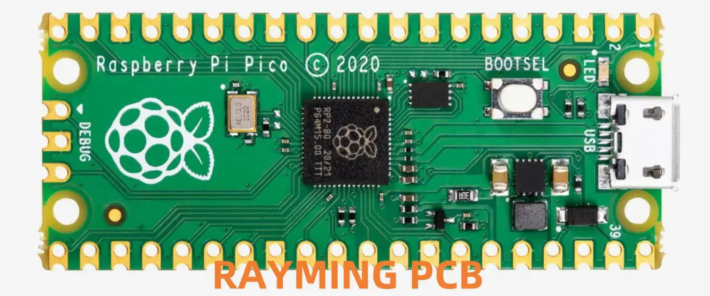
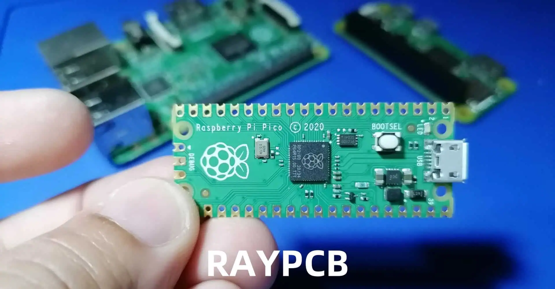
2.1 Raspberry Pi Pico

The Raspberry Pi Pico is a powerful microcontroller board based on the RP2040 chip. Its features make it ideal for IoT and home automation projects:

FeatureSpecification
ProcessorDual-core Arm Cortex-M0+ @ 133MHz
RAM264KB
Flash Memory2MB
GPIO Pins26
ADC Channels3
Operating Voltage3.3V

2.2 Temperature and Humidity Sensors

For our climate control system, we’ll use the DHT22 (also known as AM2302) sensor. It’s a popular choice for its accuracy and reliability:

FeatureSpecification
Temperature Range-40 to 80ยฐC
Humidity Range0-100% RH
Accuracy (Temp)ยฑ0.5ยฐC
Accuracy (Humidity)ยฑ2-5% RH
Resolution0.1ยฐC / 0.1% RH

2.3 Energenie Pi-mote

The Energenie Pi-mote system allows you to control electrical sockets remotely. It consists of:

  1. Energenie Pi-mote control board
  2. Radio-controlled sockets

Key features include:

  • Control up to 4 sockets independently
  • 433MHz radio frequency
  • Compatible with Raspberry Pi GPIO

3. Setting Up the Raspberry Pi Pico for Climate Control
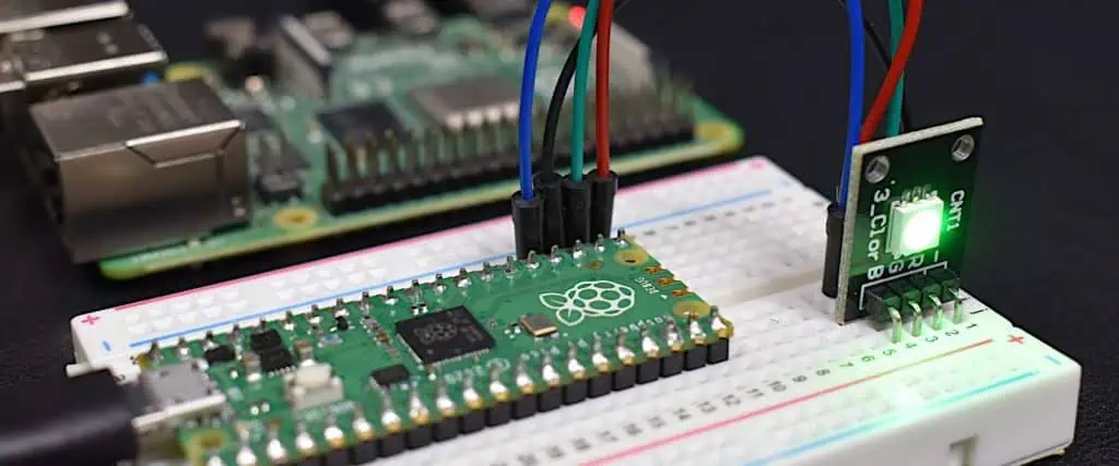
3.1 Hardware Setup

To set up the Raspberry Pi Pico for climate control:

  1. Connect the DHT22 sensor to the Pico:
    • VCC to 3.3V
    • GND to GND
    • Data to GPIO 28
  2. (Optional) Add an OLED display for real-time readings:
    • VCC to 3.3V
    • GND to GND
    • SDA to GPIO 4
    • SCL to GPIO 5

3.2 Software Setup

  1. Install MicroPython on the Raspberry Pi Pico.
  2. Install necessary libraries:
    • dht.py for the DHT22 sensor
    • ssd1306.py for the OLED display (if used)

3.3 Basic Code Structure

Here’s a basic code structure for reading temperature and humidity:

pythonCopyimport machine
import utime
from dht import DHT22

sensor = DHT22(machine.Pin(28))

while True:
    try:
        sensor.measure()
        temp = sensor.temperature()
        hum = sensor.humidity()
        print('Temperature: %3.1f C' % temp)
        print('Humidity: %3.1f %%' % hum)
    except OSError as e:
        print('Failed to read sensor.')
    
    utime.sleep(2)

4. Implementing Climate Control Logic

Raspberry Pi Pico

4.1 Defining Comfort Zones

Establish comfortable temperature and humidity ranges:

ConditionRange
Temperature20-25ยฐC
Humidity30-60%

4.2 Control Logic

Implement control logic based on sensor readings:

pythonCopydef control_climate(temp, hum):
    if temp < 20:
        # Activate heating
        pass
    elif temp > 25:
        # Activate cooling
        pass
    
    if hum < 30:
        # Activate humidifier
        pass
    elif hum > 60:
        # Activate dehumidifier
        pass

4.3 Implementing Hysteresis

To prevent rapid cycling of devices, implement hysteresis:

pythonCopyTEMP_HYSTERESIS = 1.0
HUM_HYSTERESIS = 5.0

def control_climate(temp, hum):
    global heating_on, cooling_on, humidifier_on, dehumidifier_on
    
    if temp < 20 - TEMP_HYSTERESIS and not heating_on:
        heating_on = True
        # Activate heating
    elif temp > 20 + TEMP_HYSTERESIS and heating_on:
        heating_on = False
        # Deactivate heating
    
    # Similar logic for cooling, humidifier, and dehumidifier

5. Setting Up Energenie Pi-mote

5.1 Hardware Setup

  1. Connect the Energenie Pi-mote board to the Raspberry Pi:
    • Ensure the board is properly seated on the GPIO pins
  2. Set up radio-controlled sockets:
    • Plug devices into the sockets
    • Assign each socket a unique code (1-4)

5.2 Software Setup

Install the required libraries:

bashCopysudo apt-get update
sudo apt-get install python3-rpi.gpio
sudo pip3 install energenie

5.3 Basic Control Script

Here’s a basic script to control Energenie sockets:

pythonCopyfrom energenie import switch_on, switch_off
import time

# Turn on socket 1
switch_on(1)
time.sleep(5)

# Turn off socket 1
switch_off(1)

6. Integrating Climate Control with Energenie Pi-mote

6.1 Assigning Devices to Sockets

Assign climate control devices to specific sockets:

SocketDevice
1Heater
2Air Conditioner
3Humidifier
4Dehumidifier

6.2 Updated Control Logic

Modify the control logic to activate Energenie sockets:

pythonCopyfrom energenie import switch_on, switch_off

def control_climate(temp, hum):
    if temp < 20:
        switch_on(1)  # Turn on heater
        switch_off(2)  # Turn off AC
    elif temp > 25:
        switch_off(1)  # Turn off heater
        switch_on(2)  # Turn on AC
    
    if hum < 30:
        switch_on(3)  # Turn on humidifier
        switch_off(4)  # Turn off dehumidifier
    elif hum > 60:
        switch_off(3)  # Turn off humidifier
        switch_on(4)  # Turn on dehumidifier

7. Advanced Features and Optimizations

Raspberry Pi Zero Board

7.1 Scheduling and Time-based Control

Implement time-based control for energy efficiency:

pythonCopyimport time

def time_based_control():
    current_hour = time.localtime().tm_hour
    
    if 22 <= current_hour or current_hour < 6:
        # Night-time settings
        set_temperature(18)  # Lower temperature at night
    else:
        # Day-time settings
        set_temperature(22)

7.2 Remote Monitoring and Control

Set up a simple web server for remote monitoring:

pythonCopyimport socket
import network

def setup_webserver():
    wlan = network.WLAN(network.STA_IF)
    wlan.active(True)
    wlan.connect('YOUR_SSID', 'YOUR_PASSWORD')
    
    addr = socket.getaddrinfo('0.0.0.0', 80)[0][-1]
    s = socket.socket()
    s.bind(addr)
    s.listen(1)
    
    while True:
        cl, addr = s.accept()
        # Handle client request
        cl.close()

7.3 Data Logging and Analysis

Implement data logging for long-term analysis:

pythonCopyimport ujson

def log_data(temp, hum):
    data = {'timestamp': time.time(), 'temperature': temp, 'humidity': hum}
    with open('climate_log.json', 'a') as f:
        ujson.dump(data, f)
        f.write('\n')

8. Troubleshooting and Maintenance

8.1 Common Issues and Solutions

IssuePossible CauseSolution
Inaccurate readingsSensor calibrationRecalibrate or replace sensor
Unresponsive socketsSignal interferenceCheck for obstacles, adjust antenna
System crashesMemory leaksImplement watchdog timer, optimize code

8.2 Regular Maintenance Tasks

  • Calibrate sensors every 6 months
  • Check and replace batteries in wireless devices
  • Update firmware and software regularly
  • Clean air filters in HVAC devices

9. Future Expansions and Integrations

Consider these potential expansions for your system:

  1. Integration with smart home platforms (e.g., Home Assistant, OpenHAB)
  2. Voice control through virtual assistants
  3. Machine learning for predictive climate control
  4. Energy consumption monitoring and optimization

10. Conclusion

By combining the Raspberry Pi Pico for climate sensing and control with the Energenie Pi-mote system for device automation, we’ve created a powerful and flexible home automation solution. This system not only enhances comfort but also has the potential to improve energy efficiency and provide valuable insights into your home’s climate patterns.

As you implement and expand upon this system, remember to prioritize safety, regularly maintain your devices, and stay informed about the latest developments in home automation technology. With creativity and continuous improvement, your smart home can become more intelligent, efficient, and tailored to your specific needs.

11. Frequently Asked Questions (FAQ)

  1. Q: Can this system work with other types of sensors besides the DHT22? A: Yes, the Raspberry Pi Pico is compatible with various sensors. You can use alternatives like the BME280 or SHT31 for temperature and humidity sensing. You’ll need to modify the code to work with the specific sensor’s library and pinout.
  2. Q: How many Energenie sockets can I control with one Pi-mote board? A: The standard Energenie Pi-mote board can control up to 4 individual sockets. However, there are advanced versions that can control more sockets or even work with Energenie’s smart home ecosystem for expanded control.
  3. Q: Is it possible to control the system remotely when I’m away from home? A: Yes, you can set up remote access by creating a web server on your local network and using port forwarding on your router. Alternatively, you can use cloud-based solutions like MQTT to send commands to your system from anywhere with an internet connection. Always ensure you implement proper security measures when setting up remote access.
  4. Q: How accurate is the temperature and humidity control with this setup? A: The accuracy depends on several factors, including the sensor quality, placement, and the responsiveness of your heating/cooling devices. With proper setup and calibration, you can achieve accuracy within ยฑ0.5ยฐC for temperature and ยฑ2-5% for humidity. Implementing hysteresis and proper control logic helps maintain stable conditions.
  5. Q: Can this system help reduce energy consumption? A: Yes, by maintaining optimal temperature and humidity levels and implementing features like scheduling and occupancy-based control, this system can potentially reduce energy consumption. However, the actual savings depend on various factors such as your home’s insulation, climate, and previous usage patterns. Monitoring energy consumption before and after implementation can help quantify the savings.

Key Difficulties and Tips for Backplane PCB Fabrication

Backplane Printed Circuit Boards (PCBs) are essential components in many electronic systems, serving as the backbone for interconnecting various modules and subsystems. These complex boards present unique challenges in design and fabrication due to their size, complexity, and high-performance requirements. This article will explore the key difficulties encountered in backplane PCB fabrication and provide valuable tips to overcome these challenges.

As we delve into the intricacies of backplane PCB fabrication, we’ll cover topics such as material selection, layer stackup, signal integrity, power distribution, and manufacturing considerations. By understanding these challenges and implementing the suggested solutions, engineers and PCB designers can create more reliable and efficient backplane systems.

YouTube video

2. Understanding Backplane PCBs

2.1 What is a Backplane PCB?

A backplane PCB is a large, complex circuit board that serves as the main interconnect for various daughtercards or modules in an electronic system. Backplanes are commonly used in:

  • Telecommunications equipment
  • Servers and data centers
  • Industrial control systems
  • Aerospace and defense applications

2.2 Key Characteristics of Backplane PCBs

Backplane PCBs have several distinguishing features:

CharacteristicDescription
SizeTypically larger than standard PCBs, often exceeding 24 inches in length
Layer CountHigh layer count, frequently ranging from 20 to 40 layers or more
ThicknessGreater overall thickness due to multiple layers and rigid construction
ConnectorsNumerous high-density connectors for daughtercard interfacing
Signal IntegrityCritical for high-speed data transmission across long traces
Power DistributionComplex power planes to supply various voltages to multiple modules

Understanding these characteristics is crucial for addressing the challenges in backplane PCB fabrication.

3. Key Difficulties in Backplane PCB Fabrication

3.1 Material Selection and Management

Choosing the right materials for backplane PCBs is critical due to their size and performance requirements.

3.1.1 Difficulty: Thermal Management

Backplanes generate significant heat due to their size and power requirements.

Tip: Select materials with good thermal conductivity and consider using thermal vias or embedded heat sinks.

3.1.2 Difficulty: Signal Integrity at High Frequencies

High-speed signals can degrade over long traces.

Tip: Use low-loss, high-frequency materials such as PTFE or low-loss FR-4 for critical signal layers.

3.2 Layer Stackup Design

The complex layer stackup of backplane PCBs presents several challenges.

3.2.1 Difficulty: Impedance Control

Maintaining consistent impedance across multiple layers is challenging.

Tip: Use impedance-controlled stackup design tools and work closely with your PCB manufacturer to ensure feasibility.

3.2.2 Difficulty: Inter-layer Registration

Aligning multiple layers accurately becomes more difficult with increasing layer count.

Tip: Use buried and blind vias judiciously, and consider using sequential lamination techniques for better registration.

3.3 Signal Integrity

Maintaining signal integrity over long traces and through multiple connectors is a significant challenge in backplane design.

3.3.1 Difficulty: Signal Attenuation and Distortion

Long traces can lead to signal attenuation and distortion.

Tip: Implement pre-emphasis and equalization techniques, and consider using re-driver ICs for long signal paths.

3.3.2 Difficulty: Crosstalk

Dense routing and long parallel traces increase the risk of crosstalk.

Tip: Use differential signaling, maintain proper trace spacing, and implement guard traces or ground planes between critical signals.

3.4 Power Distribution

Providing clean, stable power to multiple modules is a complex task in backplane design.

3.4.1 Difficulty: Voltage Drop

Long power distribution paths can lead to significant voltage drops.

Tip: Use thick copper planes for power distribution and implement local voltage regulation on daughtercards.

3.4.2 Difficulty: Power Plane Resonance

Large power planes can exhibit resonance at certain frequencies.

Tip: Implement stitching capacitors and use segmented power planes to reduce resonance effects.

3.5 Manufacturing Considerations

The sheer size and complexity of backplane PCBs present unique manufacturing challenges.

3.5.1 Difficulty: Warpage and Dimensional Stability

Large PCBs are prone to warpage during manufacturing processes.

Tip: Use materials with low coefficient of thermal expansion (CTE) and work with manufacturers experienced in large board production.

3.5.2 Difficulty: Plating and Aspect Ratio

High layer counts result in high aspect ratio holes, which are difficult to plate uniformly.

Tip: Design with realistic aspect ratios (typically 10:1 or less) and consider using stacked microvias for high layer count designs.

4. Advanced Tips for Backplane PCB Fabrication

4.1 Simulation and Modeling

Extensive simulation is crucial for successful backplane design.

Tip: Use 3D electromagnetic simulation tools to model critical structures and validate design choices before fabrication.

4.2 Design for Manufacturing (DFM)

Incorporating DFM principles early in the design process can significantly improve manufacturability.

Tip: Develop and maintain a close relationship with your PCB manufacturer, and involve them early in the design process for feedback on manufacturability.

4.3 Test and Verification Strategies

Comprehensive testing is essential for ensuring backplane reliability.

Tip: Implement built-in self-test (BIST) features and design for testability to facilitate thorough testing during and after manufacturing.

5. Emerging Technologies in Backplane PCB Fabrication

5.1 High-Speed Materials

New materials are being developed to support higher frequencies and lower losses.

Tip: Stay informed about new material options and their characteristics, and consider using advanced materials for critical high-speed sections of the backplane.

5.2 Embedded Passives and Actives

Embedding components within the PCB structure can improve performance and save space.

Tip: Consider using embedded capacitors for power decoupling and embedded resistors for termination networks.

5.3 Optical Interconnects

As data rates continue to increase, optical interconnects are becoming more prevalent in backplane designs.

Tip: Evaluate the potential benefits of incorporating optical interconnects for high-speed data paths, especially for longer distances within the backplane.

6. Case Studies

6.1 Case Study 1: High-Speed Telecom Backplane

A telecommunications equipment manufacturer faced challenges with signal integrity in a 40-layer backplane design.

Solution:

  • Implemented impedance-controlled differential pairs
  • Used advanced low-loss materials for critical layers
  • Incorporated re-driver ICs for long signal paths

Result: Achieved 25 Gbps data rates with excellent signal integrity across all channels.

6.2 Case Study 2: High-Reliability Aerospace Backplane

An aerospace company needed a highly reliable backplane for a mission-critical system.

Solution:

  • Used polyimide materials for improved thermal stability
  • Implemented redundant power and ground planes
  • Designed for extreme environmental conditions

Result: Produced a backplane that passed rigorous qualification testing and met all reliability requirements.

7. Future Trends in Backplane PCB Fabrication

As technology continues to advance, several trends are shaping the future of backplane PCB fabrication:

  1. Increased adoption of optical interconnects
  2. Higher integration of smart features and embedded systems
  3. Advanced materials for improved signal integrity and thermal management
  4. Greater emphasis on environmental sustainability in materials and processes

Staying abreast of these trends will be crucial for designing competitive and future-proof backplane systems.

8. Conclusion

Backplane PCB fabrication presents numerous challenges due to the complexity, size, and high-performance requirements of these critical components. By understanding the key difficulties and implementing the tips and strategies outlined in this article, designers can create more reliable, efficient, and manufacturable backplane PCBs.

Remember that successful backplane design requires a holistic approach, considering electrical, mechanical, thermal, and manufacturing aspects. Continuous learning, collaboration with manufacturers, and leveraging advanced design and simulation tools are essential for staying at the forefront of backplane PCB fabrication technology.

9. Frequently Asked Questions (FAQ)

  1. Q: What is the maximum size for a backplane PCB? A: The maximum size for a backplane PCB depends on the manufacturer’s capabilities and the specific application requirements. Some manufacturers can produce boards up to 60 inches or more in length. However, as size increases, challenges related to warpage, handling, and uniformity become more significant. It’s essential to work closely with your PCB manufacturer to determine the feasible size for your specific design.
  2. Q: How many layers are typically used in a backplane PCB? A: Backplane PCBs typically have a high layer count, often ranging from 20 to 40 layers. Some complex designs may have even more layers. The exact number depends on factors such as the required interconnect density, signal integrity requirements, and power distribution needs. It’s important to balance the layer count with manufacturability and cost considerations.
  3. Q: What are the key considerations for signal integrity in backplane design? A: Key considerations for signal integrity in backplane design include:
    • Proper impedance control
    • Minimizing crosstalk through appropriate trace spacing and shielding
    • Managing signal attenuation and distortion over long traces
    • Implementing appropriate termination strategies
    • Using differential signaling for high-speed signals
    • Careful power and ground plane design to minimize noise
  4. Q: How do you address thermal management issues in backplane PCBs? A: Thermal management in backplane PCBs can be addressed through several strategies:
    • Using materials with good thermal conductivity
    • Implementing thermal vias to conduct heat from inner layers to external layers
    • Designing with adequate copper weight for power and ground planes
    • Incorporating embedded heat sinks or thermal management layers
    • Ensuring proper airflow in the system design
    • Using thermal simulation tools to identify and address hotspots
  5. Q: What are the advantages of using optical interconnects in backplane designs? A: Optical interconnects offer several advantages in backplane designs:
    • Higher data rates over longer distances
    • Immunity to electromagnetic interference
    • Reduced power consumption compared to high-speed electrical interconnects
    • Lower latency for long-distance connections within the backplane
    • Potential for higher density interconnects However, optical interconnects also present challenges in terms of cost, integration, and interfacing with traditional electrical systems. The decision to use optical interconnects should be based on a careful analysis of the specific application requirements and overall system design.

How to Defeat Control Power Supply Grounding Defects Based on Insulation Reduction in PCB Design

In the world of Printed Circuit Board (PCB) design, one of the most critical aspects is ensuring proper grounding for control power supplies. Grounding defects can lead to a myriad of issues, including electromagnetic interference (EMI), signal integrity problems, and even system failures. This article will explore the concept of defeating control power supply grounding defects through insulation reduction techniques in PCB design.

We will delve into the fundamental principles of grounding, common defects encountered in PCB design, and how insulation reduction can be leveraged to mitigate these issues. By the end of this article, you will have a comprehensive understanding of how to implement effective grounding strategies and optimize your PCB designs for better performance and reliability.

YouTube video

2. Understanding Grounding in PCB Design

Ground a Circuit
Ground a Circuit

2.1 The Importance of Proper Grounding

Grounding is a critical aspect of PCB design that serves several essential functions:

  1. Providing a reference point for voltage measurements
  2. Establishing a return path for current flow
  3. Shielding sensitive components from electromagnetic interference
  4. Ensuring safety by providing a path for fault currents

2.2 Types of Grounding

There are several types of grounding schemes used in PCB design:

Grounding TypeDescriptionTypical Applications
Single-Point GroundingAll ground connections converge at a single pointLow-frequency circuits, analog designs
Multi-Point GroundingMultiple ground connections distributed across the boardHigh-frequency circuits, digital designs
Hybrid GroundingCombination of single-point and multi-point groundingMixed-signal designs
Floating GroundIsolated ground plane not connected to earth groundBattery-powered devices, medical equipment

2.3 Common Grounding Defects

Despite best efforts, grounding defects can still occur in PCB designs. Some common issues include:

  1. Ground loops
  2. Insufficient ground plane coverage
  3. Poor component placement
  4. Improper separation of analog and digital grounds
  5. Inadequate via placement

These defects can lead to various problems, such as increased noise, signal distortion, and reduced system performance.

3. Insulation Reduction Techniques

Insulation reduction is a strategy that can be employed to mitigate grounding defects in PCB design. By strategically reducing insulation in certain areas, we can improve grounding performance and reduce the likelihood of defects.

3.1 Principles of Insulation Reduction

The basic principle behind insulation reduction is to minimize the impedance between different ground points on the PCB. This can be achieved through various techniques:

  1. Increasing copper pour areas
  2. Optimizing stackup design
  3. Strategic via placement
  4. Implementing ground stitching
  5. Using buried and blind vias

3.2 Copper Pour Optimization

One of the most effective ways to reduce insulation and improve grounding is through optimized copper pour. This involves:

  • Maximizing ground plane coverage
  • Minimizing splits in the ground plane
  • Using thick copper for power and ground layers

3.3 Stackup Design for Improved Grounding

The PCB stackup can significantly impact grounding performance. Consider the following strategies:

LayerPurposeBenefits
Top LayerSignal routing, component placementEasy access for components
Power PlanePower distributionLow impedance power delivery
Ground PlaneReturn current pathReduced EMI, improved signal integrity
Inner Signal LayersHigh-speed signal routingShielding from external interference
Bottom LayerAdditional routing, ground planeImproved thermal management

3.4 Strategic Via Placement

Proper via placement is crucial for effective grounding. Consider these techniques:

  1. Place vias near high-frequency components
  2. Use via fencing for improved isolation
  3. Implement ground vias in a grid pattern for better current distribution

4. Implementing Insulation Reduction in PCB Design

Now that we understand the principles of insulation reduction, let’s explore how to implement these techniques in practice.

4.1 Ground Plane Design

When designing the ground plane, consider the following:

  1. Use a solid ground plane whenever possible
  2. Minimize cuts and splits in the ground plane
  3. Ensure proper ground plane coverage under high-speed signals
  4. Implement ground islands for sensitive analog circuits

4.2 Component Placement for Optimal Grounding

Proper component placement is crucial for effective grounding:

  1. Place high-frequency components close to their respective ground connections
  2. Group similar components together (analog, digital, power)
  3. Use short and wide traces for power and ground connections
  4. Implement star grounding for sensitive analog circuits

4.3 Via Stitching Techniques

Via stitching is an effective method for reducing ground impedance:

  1. Place ground vias along the edges of the board
  2. Use a grid pattern for ground via placement
  3. Implement via fencing around high-speed signal traces
  4. Place vias near decoupling capacitors for improved performance

4.4 Dealing with Mixed-Signal Designs

Mixed-signal designs present unique challenges for grounding. Consider these strategies:

  1. Separate analog and digital grounds
  2. Use a split ground plane with a single connection point
  3. Implement guard traces around sensitive analog signals
  4. Use dedicated power and ground planes for analog and digital sections

5. Advanced Techniques for Grounding Defect Mitigation

5.1 Electromagnetic Bandgap (EBG) Structures

EBG structures can be used to suppress electromagnetic interference:

  1. Implement periodic structures in the ground plane
  2. Use EBG structures to isolate noisy components
  3. Design custom EBG patterns for specific frequency ranges

5.2 Embedded Capacitance

Embedded capacitance can improve power delivery and reduce ground bounce:

  1. Use thin dielectric materials between power and ground planes
  2. Implement embedded capacitance in critical areas of the board
  3. Combine embedded capacitance with strategic decoupling capacitor placement

5.3 Ground Plane Stitching

Ground plane stitching can help reduce ground impedance in multi-layer designs:

  1. Use multiple vias to connect ground planes on different layers
  2. Implement a stitching pattern that follows high-speed signal paths
  3. Combine ground plane stitching with via fencing for improved isolation

6. Verification and Testing

After implementing insulation reduction techniques, it’s crucial to verify and test the design:

6.1 Simulation and Analysis

Use electromagnetic simulation tools to:

  1. Analyze current distribution in the ground plane
  2. Identify potential EMI hotspots
  3. Verify signal integrity for critical traces

6.2 Physical Testing

Perform physical tests to ensure proper grounding:

  1. Use a vector network analyzer to measure impedance
  2. Conduct EMI/EMC testing to verify compliance with regulations
  3. Perform functional testing under various operating conditions

7. Case Studies

To illustrate the effectiveness of insulation reduction techniques, consider the following case studies:

7.1 Case Study 1: High-Speed Digital Design

A high-speed digital design experienced signal integrity issues due to grounding defects. By implementing the following insulation reduction techniques, the problems were resolved:

  1. Optimized stackup with dedicated ground planes
  2. Implemented via stitching around high-speed traces
  3. Used embedded capacitance for improved power delivery

Results:

  • 40% reduction in EMI emissions
  • Improved signal integrity with reduced jitter
  • Enhanced overall system performance

7.2 Case Study 2: Mixed-Signal Audio Circuit

A mixed-signal audio circuit suffered from noise and crosstalk issues. The following techniques were applied:

  1. Separated analog and digital grounds with a single connection point
  2. Implemented guard traces around sensitive analog signals
  3. Used a combination of single-point and multi-point grounding

Results:

  • 25 dB improvement in signal-to-noise ratio
  • Eliminated audible crosstalk between channels
  • Achieved compliance with audio equipment standards

8. Conclusion

Defeating control power supply grounding defects through insulation reduction techniques is a crucial aspect of modern PCB design. By implementing the strategies discussed in this article, designers can significantly improve the performance, reliability, and electromagnetic compatibility of their circuits.

Remember that effective grounding is not a one-size-fits-all solution. Each design requires careful consideration of its unique requirements and constraints. Continuously educate yourself on new techniques and technologies to stay at the forefront of PCB design best practices.

9. Frequently Asked Questions (FAQ)

  1. Q: What is the most common grounding defect in PCB design? A: The most common grounding defect is often ground loops, which occur when there are multiple paths for current to flow back to the source, potentially creating unwanted voltage differences and noise.
  2. Q: How does insulation reduction help with grounding defects? A: Insulation reduction techniques, such as optimizing copper pours and via placement, help minimize the impedance between different ground points on the PCB. This reduces the likelihood of voltage differences and improves overall grounding performance.
  3. Q: Can I use a single ground plane for both analog and digital circuits? A: While it’s possible, it’s generally not recommended for sensitive mixed-signal designs. Separating analog and digital grounds with a single connection point (split ground plane) is often a better approach to minimize noise coupling between the two domains.
  4. Q: How do I determine the optimal number of ground vias to use in my design? A: The optimal number of ground vias depends on factors such as board size, frequency of operation, and current requirements. A general rule of thumb is to place ground vias every quarter-wavelength of the highest frequency of interest, but electromagnetic simulation can provide more accurate guidance for your specific design.
  5. Q: What are the signs of poor grounding in a PCB design? A: Signs of poor grounding can include excessive EMI emissions, signal integrity issues (such as ringing or reflections), unexpected voltage drops, and system instability. These issues may manifest as intermittent failures, noise in analog signals, or reduced performance in high-speed digital circuits.

SMT Assembly Process Optimization by Multi-head Gantry-Type Chip Mounter

Surface Mount Technology (SMT) has revolutionized electronic manufacturing, enabling the production of smaller, more complex, and highly efficient electronic devices. At the heart of SMT assembly lies the chip mounter, a crucial piece of equipment responsible for accurately placing components onto printed circuit boards (PCBs). Among various types of chip mounters, the multi-head gantry-type chip mounter stands out for its high speed and precision, making it an ideal choice for high-volume production environments.

This article delves into the optimization of SMT assembly processes using multi-head gantry-type chip mounters. We will explore various strategies, techniques, and technologies that can significantly enhance production efficiency, reduce errors, and improve overall product quality.

Understanding Multi-head Gantry-Type Chip Mounters

Basic Principles

Multi-head gantry-type chip mounters are advanced pick-and-place machines designed for high-speed, high-precision component placement in SMT assembly lines. These machines typically feature:

  1. A gantry system for X-Y axis movement
  2. Multiple placement heads mounted on the gantry
  3. A variety of nozzle types for handling different component sizes and shapes
  4. Advanced vision systems for component recognition and alignment
  5. Sophisticated software for optimizing placement sequences and machine movements

Advantages of Multi-head Gantry-Type Chip Mounters

AdvantageDescription
High SpeedMultiple heads allow simultaneous pick-and-place operations, significantly increasing throughput
FlexibilityCan handle a wide range of component types and sizes
PrecisionAdvanced vision systems and motion control ensure high placement accuracy
ScalabilityEasily adaptable to different production volumes and product types
EfficiencyOptimized movements and parallel operations reduce cycle times

Understanding these fundamental aspects is crucial for implementing effective optimization strategies in SMT assembly processes.

Key Components of a Multi-head Gantry-Type Chip Mounter

To optimize the SMT assembly process, it’s essential to understand the key components of a multi-head gantry-type chip mounter and their roles in the overall system.

1. Gantry System

The gantry system provides the main framework for the chip mounter, enabling precise X-Y axis movement.

  • X-axis: Typically the longer axis, allowing movement across the width of the PCB
  • Y-axis: Allows movement along the length of the PCB
  • Z-axis: Vertical movement for component pickup and placement

2. Placement Heads

Multiple placement heads are mounted on the gantry, each capable of independent movement and component placement.

  • Number of Heads: Typically ranges from 2 to 24, depending on the machine model
  • Head Types: Can include fixed heads, rotating heads, or a combination

3. Nozzles

Nozzles are responsible for picking up and placing components. Different nozzle types are used for various component sizes and shapes.

  • Nozzle Types: Include vacuum nozzles, mechanical grippers, and specialized nozzles for odd-shaped components
  • Nozzle Change System: Allows quick and automatic nozzle changes during operation

4. Feeder Systems

Feeders supply components to the placement heads. Various types of feeders are used depending on the component packaging.

  • Tape Feeders: For components in tape and reel packaging
  • Tray Feeders: For larger or tray-packaged components
  • Tube Feeders: For components supplied in tubes
  • Bulk Feeders: For small, loose components

5. Vision System

The vision system is crucial for component recognition, alignment, and placement verification.

  • Upward-looking Camera: For component pickup inspection and alignment
  • Downward-looking Camera: For PCB fiducial recognition and placement verification
  • High-speed Image Processing: For real-time component and feature recognition

6. Control System

The control system manages all aspects of the chip mounter’s operation.

  • Main Controller: Coordinates all machine functions and optimizes placement sequences
  • Motion Controllers: Manage the precise movements of the gantry and placement heads
  • User Interface: Allows operators to program and monitor the machine

7. Conveyor System

The conveyor system transports PCBs through the chip mounter.

  • Input Buffer: Holds PCBs waiting to enter the placement area
  • Placement Area: Where components are placed on the PCB
  • Output Buffer: Holds completed PCBs

Component Specifications Table

ComponentKey SpecificationsTypical Range
Gantry SystemAcceleration, Maximum Speed1-3 G, 1-2 m/s
Placement HeadsNumber of Heads, Rotation Speed2-24 heads, 2-3 rotations/s
NozzlesDiameter Range, Pickup Force0.3-6 mm, 1-10 N
FeedersTape Width, Pitch8-56 mm, 2-72 mm
Vision SystemResolution, Processing Speed5-20  ฮผm, 50-200 ms/frame
Control SystemCPU Speed, Memory2-4 GHz, 16-64 GB RAM
Conveyor SystemWidth Range, Transport Speed50-460 mm, 1-2 m/min

Understanding these key components and their specifications is crucial for implementing effective optimization strategies in the SMT assembly process using multi-head gantry-type chip mounters.

Optimization Strategies for SMT Assembly

Optimizing the SMT assembly process using multi-head gantry-type chip mounters involves a multifaceted approach that addresses various aspects of the production line. This section outlines key strategies for enhancing efficiency, accuracy, and overall productivity.

1. Component Placement Optimization

Efficient component placement is crucial for maximizing throughput and minimizing cycle times.

  • Intelligent Grouping: Group components based on size, type, and placement location
  • Dynamic Head Assignment: Optimize the use of multiple heads for parallel operations
  • Path Optimization: Minimize head travel distances and optimize placement sequences

2. Feeder Arrangement and Management

Proper feeder setup and management can significantly impact machine efficiency.

  • Strategic Feeder Placement: Arrange feeders to minimize pick-up distances
  • Component Family Grouping: Group similar components for efficient nozzle utilization
  • Just-in-Time Feeder Replenishment: Implement systems for timely feeder refills

3. Vision System Enhancements

Improving vision system performance can lead to faster and more accurate placements.

  • Advanced Algorithms: Implement state-of-the-art image processing algorithms
  • Multi-camera Integration: Use multiple cameras for simultaneous inspections
  • Adaptive Lighting: Optimize lighting conditions for different component types

4. Motion Control and Path Optimization

Enhancing motion control can lead to smoother, faster movements and reduced cycle times.

  • Acceleration Profile Optimization: Fine-tune acceleration and deceleration profiles
  • Jerk Control: Implement advanced motion control algorithms to reduce vibration
  • Predictive Path Planning: Use AI algorithms for optimal path generation

5. Nozzle Selection and Management

Efficient nozzle management is crucial for handling diverse component types.

  • Automated Nozzle Selection: Implement intelligent nozzle selection algorithms
  • Nozzle Wear Monitoring: Use sensors to detect and predict nozzle wear
  • Quick-change Nozzle Systems: Minimize downtime during nozzle changes

6. Production Planning and Scheduling

Effective planning can optimize machine utilization and reduce changeover times.

  • Intelligent Job Sequencing: Group similar jobs to minimize setup changes
  • Real-time Production Monitoring: Implement systems for live production tracking
  • Predictive Maintenance Scheduling: Use data analytics to schedule maintenance

7. Machine Learning and AI Integration

Leveraging advanced algorithms can lead to continuous process improvements.

  • Self-optimizing Systems: Implement machine learning for ongoing process refinement
  • Predictive Error Detection: Use AI to anticipate and prevent potential errors
  • Adaptive Process Control: Dynamically adjust parameters based on real-time data

Optimization Strategy Impact Table

StrategyPotential ImpactImplementation ComplexityROI Timeframe
Component Placement OptimizationHighMediumShort-term
Feeder Arrangement and ManagementMediumLowShort-term
Vision System EnhancementsHighHighMedium-term
Motion Control and Path OptimizationMediumHighMedium-term
Nozzle Selection and ManagementMediumMediumShort-term
Production Planning and SchedulingHighMediumMedium-term
Machine Learning and AI IntegrationVery HighVery HighLong-term

By implementing these optimization strategies, manufacturers can significantly enhance the performance of their multi-head gantry-type chip mounters, leading to improved productivity, reduced errors, and increased overall efficiency in the SMT assembly process.

Component Placement Optimization

High Volume Assembly Line

Component placement optimization is a critical aspect of improving the efficiency of multi-head gantry-type chip mounters in SMT assembly. This section delves into specific techniques and strategies for optimizing the component placement process.

1. Intelligent Component Grouping

Grouping components based on their characteristics and placement requirements can significantly reduce cycle times and improve overall efficiency.

Grouping Criteria:

  • Component size and type
  • Placement location on the PCB
  • Required nozzle type
  • Placement force and speed requirements

Benefits of Intelligent Grouping:

  • Minimizes nozzle changes
  • Reduces head travel distances
  • Allows for parallel placements by multiple heads

2. Dynamic Head Assignment

Optimizing the use of multiple placement heads is crucial for maximizing throughput.

Strategies for Dynamic Head Assignment:

  • Assign components to heads based on their proximity and grouping
  • Balance workload across all available heads
  • Dynamically reassign tasks to idle heads to minimize wait times

Head Assignment Optimization Algorithm:

  1. Analyze component placement map
  2. Group components based on proximity and type
  3. Assign groups to heads considering travel distances and nozzle compatibility
  4. Continuously reassess and adjust assignments during operation

3. Path Optimization

Minimizing head travel distances and optimizing placement sequences can significantly reduce cycle times.

Path Optimization Techniques:

  • Implement advanced pathfinding algorithms (e.g., modified Traveling Salesman Problem solutions)
  • Consider component height and placement order to avoid collisions
  • Optimize Z-axis movements for efficient pick-and-place operations

Path Optimization Metrics:

  • Total travel distance
  • Number of direction changes
  • Z-axis movement efficiency

4. Component-specific Placement Strategies

Tailoring placement strategies to specific component types can improve both speed and accuracy.

Component TypePlacement StrategyBenefits
Fine-pitch ICsSlow, precise placement with vision assistanceImproved accuracy, reduced placement errors
Large ComponentsUse of specialized nozzles, adjusted placement forceBetter handling, reduced risk of damage
Small Passive ComponentsHigh-speed placement, gang pick-upIncreased throughput for high-volume components
Odd-shaped ComponentsCustom nozzles, adjusted placement parametersImproved handling of non-standard parts

5. Placement Sequence Optimization

Optimizing the order in which components are placed can lead to significant efficiency gains.

Sequence Optimization Considerations:

  • Minimize nozzle changes
  • Reduce head travel distances
  • Consider component dependencies (e.g., taller components placed after shorter ones)
  • Balance workload across multiple heads

Sequence Optimization Algorithm:

  1. Create initial sequence based on component locations
  2. Apply local optimization techniques (e.g., 2-opt, 3-opt swaps)
  3. Consider constraints (nozzle changes, component height)
  4. Iteratively improve sequence using metaheuristic algorithms (e.g., Genetic Algorithms, Simulated Annealing)

6. Real-time Adjustment and Adaptation

Implementing systems for real-time optimization can help adapt to changing conditions during production.

Real-time Optimization Strategies:

  • Continuous monitoring of placement accuracy and speed
  • Dynamic adjustment of placement parameters based on feedback
  • Real-time resequencing to account for unexpected events (e.g., component shortages, feeder issues)

Component Placement Optimization Impact

Optimization TechniquePotential Throughput IncreaseAccuracy ImprovementImplementation Complexity
Intelligent Grouping10-20%ModerateMedium
Dynamic Head Assignment15-25%MinimalHigh
Path Optimization5-15%MinimalMedium
Component-specific Strategies5-10%SignificantMedium
Sequence Optimization10-20%ModerateHigh
Real-time Adjustment5-10%SignificantVery High

By implementing these component placement optimization techniques, manufacturers can significantly enhance the performance of their multi-head gantry-type chip mounters. The combined effect of these strategies can lead to substantial improvements in throughput, accuracy, and overall efficiency of the SMT assembly process.

Feeder Arrangement and Management

Efficient feeder arrangement and management are crucial for optimizing the performance of multi-head gantry-type chip mounters in SMT assembly. This section explores strategies and techniques for improving feeder setup and operation.

1. Strategic Feeder Placement

Proper placement of feeders can significantly reduce pick-up times and improve overall machine efficiency.

Feeder Placement Strategies:

  • Place high-usage components closest to the center of the pickup area
  • Group similar component types together
  • Consider the PCB layout when arranging feeders
  • Minimize head travel distances for frequently used components

Feeder Placement Optimization Algorithm:

  1. Analyze component usage frequency from production data
  2. Rank components based on usage and criticality
  3. Assign optimal feeder slots based on ranking and physical constraints
  4. Iteratively refine placement to minimize overall travel distance

2. Component Family Grouping

Grouping similar components can lead to more efficient nozzle utilization and reduced setup times.

Grouping Criteria:

  • Component size and shape
  • Required nozzle type
  • Placement force and speed requirements
  • Packaging type (tape and reel, tray, tube)

Benefits of Component Family Grouping:

  • Minimizes nozzle changes
  • Simplifies feeder setup and changeover
  • Improves overall pick-and-place efficiency

3. Just-in-Time Feeder Replenishment

Implementing systems for timely feeder refills can minimize machine downtime and maintain continuous operation.

JIT Replenishment Strategies:

  • Use smart feeders with component level monitoring
  • Implement warning systems for low component levels
  • Develop standardized procedures for quick feeder changes
  • Train operators in efficient replenishment techniques

JIT Replenishment Workflow:

  1. Continuous monitoring of component levels
  2. Automated alerts for low-stock situations
  3. Preparation of replacement feeders off-line
  4. Quick-swap procedures for minimal production interruption

4. Intelligent Feeder Management Systems

Advanced feeder management systems can significantly improve setup times and reduce errors.

Key Features of Intelligent Feeder Management:

  • RFID or barcode tracking for individual feeders
  • Automated feeder

Design and Implementation of High Density FDR Interconnection Switch Boards

High Density FDR (Fourteen Data Rate) Interconnection Switch Boards are at the forefront of high-speed data communication technology. These advanced boards play a crucial role in modern data centers, high-performance computing systems, and telecommunications infrastructure. This article delves into the intricate design and implementation aspects of these complex systems, exploring the challenges and solutions in creating efficient, reliable, and high-performance FDR switch boards.

YouTube video

Understanding FDR Technology

What is FDR?

FDR, or Fourteen Data Rate, is an InfiniBand specification that supports data rates up to 14 Gbps per lane. It’s a significant advancement over previous generations, offering increased bandwidth and improved efficiency for high-performance computing and data center applications.

Key Features of FDR

  1. Data Rate: 14 Gbps per lane
  2. Aggregated Bandwidth: Up to 168 Gbps (12 lanes)
  3. Low Latency: Typically sub-microsecond
  4. Enhanced Error Correction: Improved reliability
  5. Backward Compatibility: With previous InfiniBand standards

Comparison of InfiniBand Standards

StandardData Rate (per lane)Max Aggregate Bandwidth (12 lanes)Year Introduced
SDR2.5 Gbps30 Gbps2001
DDR5 Gbps60 Gbps2005
QDR10 Gbps120 Gbps2008
FDR14 Gbps168 Gbps2011
EDR25 Gbps300 Gbps2014
HDR50 Gbps600 Gbps2017

Understanding these fundamental aspects of FDR technology is crucial for designing and implementing high-density interconnection switch boards.

Key Design Considerations

Designing high-density FDR interconnection switch boards requires careful consideration of various factors to ensure optimal performance, reliability, and manufacturability. Here are the key design considerations:

1. High-Speed Signal Integrity

  • Impedance control
  • Signal routing and trace length matching
  • Minimizing crosstalk and electromagnetic interference (EMI)
  • Proper termination and return path design

2. Density and Form Factor

  • Maximizing port density while maintaining signal integrity
  • Efficient use of PCB real estate
  • Considerations for cooling and airflow

3. Power Distribution

  • Clean and stable power delivery to all components
  • Proper decoupling and bypass capacitor placement
  • Power plane design and current capacity

4. Thermal Management

  • Heat dissipation strategies for high-power components
  • Thermal modeling and analysis
  • Integration of cooling solutions (e.g., heatsinks, fans)

5. Manufacturability and Testability

  • Design for manufacturing (DFM) considerations
  • Implementation of test points and debug features
  • Compliance with industry standards and regulations

6. Scalability and Modularity

  • Design for future upgrades and expansion
  • Modular architecture for easier maintenance and replacement

7. Cost Optimization

  • Balance between performance and cost
  • Component selection and sourcing strategies

8. Reliability and Longevity

  • Component lifecycle management
  • Redundancy and fault tolerance features
  • Environmental considerations (temperature, humidity, vibration)

By addressing these key design considerations, engineers can create high-density FDR interconnection switch boards that meet the demanding requirements of modern high-performance computing and data center environments.

PCB Layout and Routing Strategies

Effective PCB layout and routing are crucial for the performance and reliability of high-density FDR interconnection switch boards. This section explores strategies and best practices for achieving optimal layout and routing.

Layer Stack-up Design

The layer stack-up is fundamental to the PCB design and affects signal integrity, power distribution, and overall performance.

Typical High-Speed Layer Stack-up

LayerFunction
1Signal (Top)
2Ground
3Signal
4Power
5Ground
6Signal
n-1Ground
nSignal (Bottom)
  • Use multiple ground planes for improved return path and EMI shielding
  • Alternate signal and ground layers for better impedance control
  • Place power planes strategically to minimize power distribution network (PDN) impedance

High-Speed Routing Techniques

  1. Controlled Impedance Routing
    • Maintain consistent trace width and spacing
    • Use impedance calculators to determine optimal trace geometries
  2. Length Matching
    • Match trace lengths within differential pairs and between pairs in a bus
    • Implement serpentine routing for length equalization
  3. Differential Pair Routing
    • Keep differential pairs tightly coupled
    • Maintain symmetry in routing and layer transitions
  4. Via Management
    • Minimize the use of vias in high-speed paths
    • Use back-drilling for stub reduction in thick boards
    • Implement via stitching for improved return path and EMI shielding
  5. Guard Traces and Shielding
    • Use guard traces between sensitive signals
    • Implement ground planes and stitching vias for shielding

Component Placement Strategies

  1. Logical Grouping
    • Place related components close together to minimize trace lengths
    • Consider signal flow and data path optimization
  2. Thermal Considerations
    • Distribute heat-generating components to avoid hotspots
    • Allow space for thermal management solutions
  3. EMI Mitigation
    • Separate analog and digital circuits
    • Keep noisy components (e.g., switching regulators) away from sensitive circuits
  4. Serviceability
    • Place debug and test points in accessible locations
    • Consider modular design for easier maintenance and upgrades

Routing Guidelines for FDR Signals

ParameterGuideline
Differential Impedance100 ฮฉ ยฑ10%
Trace WidthTypically 3-5 mils (depends on stack-up)
Trace SpacingTypically 4-6 mils (depends on stack-up)
Max Length Mismatch< 5 mils within a pair, < 25 mils between pairs
Max Via Countโ‰ค 2 per signal path (if unavoidable)
Guard Trace Spacing3x trace width (minimum)

Advanced Routing Techniques

  1. Embedded Passives
    • Integrate resistors and capacitors within PCB layers
    • Reduce board space and improve signal integrity
  2. Coplanar Waveguide Structures
    • Implement for improved impedance control and reduced crosstalk
    • Useful for ultra-high-speed signals and transitions
  3. Micro Via Technology
    • Use for high-density interconnects
    • Improve signal integrity by reducing via stub effects

By implementing these PCB layout and routing strategies, designers can create high-density FDR interconnection switch boards that meet the stringent requirements for signal integrity, performance, and reliability in demanding high-speed applications.

Signal Integrity and EMI Considerations

Ensuring signal integrity and minimizing electromagnetic interference (EMI) are critical aspects of designing high-density FDR interconnection switch boards. This section explores key considerations and techniques for maintaining signal quality and reducing EMI in these high-speed designs.

Signal Integrity Challenges in FDR Designs

  1. Attenuation: Signal loss due to conductor and dielectric losses
  2. Reflection: Impedance discontinuities causing signal reflections
  3. Crosstalk: Unwanted coupling between adjacent signals
  4. Jitter: Timing variations in signal edges
  5. Inter-Symbol Interference (ISI): Distortion of signals due to bandwidth limitations

Techniques for Improving Signal Integrity

1. Impedance Control

  • Maintain consistent impedance throughout signal paths
  • Use impedance-controlled PCB fabrication processes
  • Implement proper termination strategies

2. Equalization Techniques

  • Implement pre-emphasis at the transmitter
  • Use adaptive equalization at the receiver
  • Consider channel-based equalization for long traces

3. Jitter Mitigation

  • Optimize clock distribution networks
  • Use low-jitter clock sources and PLLs
  • Implement proper power supply decoupling

4. Crosstalk Reduction

  • Optimize trace spacing and layer assignments
  • Use guard traces and ground planes for isolation
  • Implement differential signaling for improved noise immunity

EMI Mitigation Strategies

1. Board-Level Shielding

  • Use ground planes and power planes for shielding
  • Implement ground stitching vias around high-speed areas
  • Consider embedded shield layers for critical signals

2. Component-Level Shielding

  • Use shielded connectors and cable assemblies
  • Implement local shielding for noisy or sensitive components
  • Consider EMI suppression components (e.g., ferrite beads, common-mode chokes)

3. Filtering and Decoupling

  • Implement proper power supply filtering
  • Use adequate bypass capacitors for all ICs
  • Consider bulk decoupling for power distribution networks

4. Edge Rate Control

  • Optimize driver slew rates to reduce EMI
  • Use series termination to control edge rates
  • Consider spread spectrum clocking techniques

Signal Integrity Analysis Tools and Techniques

  1. Time Domain Reflectometry (TDR)
    • Analyze impedance discontinuities along signal paths
    • Identify and locate signal integrity issues
  2. Vector Network Analysis (VNA)
    • Measure S-parameters for high-speed channels
    • Characterize frequency domain behavior of signals
  3. Eye Diagram Analysis
    • Assess overall signal quality and timing margins
    • Identify issues such as jitter, noise, and ISI
  4. Electromagnetic Field Simulation
    • Perform full-wave analysis of complex structures
    • Predict EMI and crosstalk behavior

EMC Compliance Considerations

Ensuring electromagnetic compatibility (EMC) is crucial for FDR switch boards to meet regulatory requirements and function reliably in various environments.

EMC Standards Relevant to FDR Switch Boards

StandardDescriptionRelevance
FCC Part 15US EMC regulationsEmissions limits for digital devices
CISPR 22/EN 55022International EMC standardIT equipment emissions requirements
IEC 61000-4-xImmunity test standardsVarious immunity tests (ESD, radiated, conducted)
EN 55024IT equipment immunitySpecific requirements for IT equipment

EMC Design Checklist

  1. Implement a solid grounding strategy
  2. Use proper shielding techniques
  3. Optimize component placement for EMI reduction
  4. Implement filtering on all I/O and power connections
  5. Consider EMC requirements early in the design process
  6. Perform pre-compliance testing during development
  7. Design with margins to account for manufacturing variations

By addressing these signal integrity and EMI considerations, designers can create high-density FDR interconnection switch boards that not only meet performance requirements but also comply with relevant EMC standards and regulations.

Power Distribution and Thermal Management

Effective power distribution and thermal management are critical for the reliable operation of high-density FDR interconnection switch boards. This section explores strategies and best practices for designing robust power delivery systems and managing heat dissipation in these complex, high-speed designs.

Power Distribution Network (PDN) Design

1. Power Budgeting

  • Calculate total power requirements for all components
  • Account for variations in power consumption under different operating conditions
  • Include margin for future upgrades or expanded functionality

2. Voltage Regulation

  • Select appropriate voltage regulators for each power rail
  • Consider using distributed power architecture for improved efficiency
  • Implement point-of-load (POL) regulation for noise-sensitive components

3. Power Plane Design

  • Use dedicated power planes for each voltage rail
  • Implement split planes to isolate noisy and sensitive circuits
  • Consider using buried capacitance technology for improved PDN performance

4. Decoupling Strategy

  • Use a multi-tiered decoupling approach:
    • Bulk decoupling at power entry points
    • Local decoupling near voltage regulators
    • High-frequency decoupling at IC power pins
  • Select appropriate capacitor types and values based on frequency requirements

Power Distribution Components Selection

Component TypeConsiderationsExamples
Voltage RegulatorsEfficiency, thermal performance, output current, noiseLinear (LDO), Switching (Buck, Boost)
Decoupling CapacitorsCapacitance, ESR, resonant frequency, sizeCeramic (X5R, X7R), Tantalum, Polymer
Power InductorsInductance, DCR, saturation current, sizeShielded, Unshielded, Molded, Toroidal
Power ConnectorsCurrent rating, insertion/extraction force, durabilityATX, PCIe, Custom high-current

Thermal Management Strategies

1. Thermal Modeling and Analysis

  • Perform detailed thermal simulations using CFD tools
  • Identify hotspots and areas of concern
  • Optimize component placement and board layout for improved heat dissipation

2. Heat Spreading Techniques

  • Use thick copper planes for improved lateral heat spreading
  • Consider embedding heat spreading layers (e.g., copper coins) in PCB stack-up
  • Implement thermal vias under high-power components

3. Active Cooling Solutions

  • Design for proper airflow channels across the board
  • Select appropriate fans or blowers based on airflow and noise requirements
  • Consider liquid cooling for extreme high-power applications

4. Passive Cooling Techniques

  • Use appropriately sized heatsinks for high-power components
  • Implement thermal interface materials (TIMs) for improved heat transfer
  • Consider heat pipes or vapor chambers for efficient heat removal

Thermal Design Considerations Table

ComponentThermal ConsiderationMitigation Strategy
High-Speed SerDesJunction temperature < 105ยฐCHeatsink, airflow optimization
Voltage RegulatorsKeep FETs and inductors coolCopper spreading, thermal vias
Memory DevicesEnsure uniform cooling across arraysEven airflow distribution
ConnectorsManage heat in high-current pathsThick copper, thermal reliefs
PCB SubstrateAvoid excessive layer-to-layer gradientsBalanced stack-up design

Power Integrity Analysis Techniques

  1. DC Analysis
    • Verify voltage drop across power planes
    • Ensure sufficient current-carrying capacity in planes and traces
  2. AC Analysis
    • Analyze PDN impedance across frequency range
    • Identify and mitigate resonances in the power delivery system
  3. Transient Analysis
    • Simulate dynamic load conditions
    • Verify power supply response to fast load changes

Thermal Testing and Verification

  1. Infrared Thermography
    • Capture real-time thermal images of operating boards
    • Identify hotspots and validate thermal models
  2. Thermocouple Measurements
    • Place thermocouples at critical points for accurate temperature readings
    • Verify compliance with component thermal specifications
  3. Thermal Cycling and Stress Testing
    • Perform accelerated life testing under various thermal conditions
    • Validate long-term reliability of thermal design

By implementing these power distribution and thermal management strategies,

Effective Measures for Quality Control on Ball Grid Array (BGA) Solder Joints

Ball Grid Array (BGA) technology has become increasingly prevalent in modern electronics manufacturing due to its ability to provide high-density interconnections in a compact footprint. However, the complexity of BGA solder joints presents unique challenges in terms of quality control. Ensuring the reliability and integrity of these connections is crucial for the overall performance and longevity of electronic devices. This article explores effective measures for implementing robust quality control processes for BGA solder joints, covering various stages of production and utilizing advanced inspection techniques.

YouTube video

Understanding BGA Technology

What is a Ball Grid Array?

A Ball Grid Array is a type of surface-mount packaging used for integrated circuits. It uses an array of solder balls arranged in a grid pattern on the underside of the package to establish electrical connections with the printed circuit board (PCB).

Advantages of BGA Technology

  1. Higher pin count in a smaller package
  2. Improved electrical performance due to shorter connections
  3. Better heat dissipation
  4. Self-alignment properties during reflow

Challenges in BGA Soldering

  1. Hidden solder joints making visual inspection difficult
  2. Increased complexity in the soldering process
  3. Higher sensitivity to thermal stress
  4. Potential for warpage and coplanarity issues

Understanding these fundamentals is crucial for implementing effective quality control measures throughout the BGA soldering process.

Common Defects in BGA Solder Joints

Before delving into quality control measures, it’s essential to understand the types of defects that can occur in BGA solder joints. This knowledge forms the basis for developing targeted inspection and prevention strategies.

Types of BGA Solder Joint Defects

  1. Open Joints: Lack of electrical connection between the BGA ball and the PCB pad.
  2. Bridging: Unwanted connection between adjacent solder balls.
  3. Head-on-Pillow: Incomplete coalescence between the BGA ball and the solder paste.
  4. Voids: Gas pockets within the solder joint, reducing its strength and conductivity.
  5. Insufficient Solder: Not enough solder to form a reliable connection.
  6. Excess Solder: Too much solder, potentially leading to bridging or altered joint geometry.
  7. Cracked Joints: Fractures in the solder joint, often due to thermal or mechanical stress.
  8. Misalignment: Improper positioning of the BGA package on the PCB.

Defect Classification Table

Defect TypeSeverityCommon CausesPotential Impacts
Open JointsHighInsufficient solder, poor wetting, warpageComplete failure of affected connections
BridgingHighExcess solder, improper stencil designShort circuits, functional failures
Head-on-PillowMedium-HighWarpage, improper reflow profileIntermittent connections, reduced reliability
VoidsLow-MediumOutgassing, improper flux chemistryReduced joint strength, potential long-term reliability issues
Insufficient SolderMediumIncorrect solder paste volume, poor wettingWeak joints, potential open connections
Excess SolderMediumOverfilled stencil apertures, improper stencil designRisk of bridging, altered joint geometry
Cracked JointsHighThermal stress, mechanical shockIntermittent or complete connection failure
MisalignmentHighPick-and-place errors, poor component designMultiple defects, functional failures

Understanding these defects and their potential impacts is crucial for developing a comprehensive quality control strategy for BGA solder joints.

Pre-Soldering Quality Control Measures

Implementing quality control measures before the soldering process begins is crucial for preventing defects and ensuring optimal conditions for successful BGA attachment. These pre-soldering measures focus on component preparation, PCB quality, and process parameter verification.

1. BGA Component Inspection

Visual Inspection

  • Check for any visible damage to the BGA package
  • Verify correct part number and specifications
  • Inspect for signs of oxidation or contamination on solder balls

Coplanarity Check

  • Use automated optical inspection (AOI) or coordinate measuring machines (CMM) to verify ball coplanarity
  • Ensure compliance with manufacturer specifications for ball height variation

2. PCB Quality Assurance

Pad Design and Finish

  • Verify correct pad size, shape, and finish according to BGA specifications
  • Inspect solder mask defined (SMD) vs. non-solder mask defined (NSMD) pad designs
  • Check for proper surface finish (e.g., ENIG, OSP) and cleanliness

PCB Flatness

  • Measure PCB warpage using vision systems or flatness gauges
  • Ensure compliance with IPC standards for maximum allowable warpage

3. Solder Paste Inspection

Solder Paste Composition

  • Verify correct solder alloy and flux composition for the BGA application
  • Check solder paste expiration date and storage conditions

Stencil Design Verification

  • Confirm stencil aperture size and shape match BGA pad design
  • Verify stencil thickness is appropriate for required solder volume

4. Process Parameter Verification

Reflow Profile Optimization

  • Develop and verify reflow profile using thermocouples or profiling systems
  • Ensure profile meets BGA manufacturer’s recommendations for temperature and time

Pick-and-Place Machine Calibration

  • Verify pick-and-place machine accuracy and repeatability
  • Calibrate placement force and alignment systems

5. Environmental Control

Humidity and Temperature Monitoring

  • Implement controls to maintain recommended humidity levels (typically 30-60% RH)
  • Ensure stable ambient temperature in the production area

ESD Protection Measures

  • Verify proper ESD protection equipment and procedures are in place
  • Conduct regular ESD audits and staff training

Pre-Soldering Quality Control Checklist

CategoryCheck PointAcceptance Criteria
BGA ComponentVisual InspectionNo visible damage or contamination
CoplanarityWithin ยฑX ฮผm (as per manufacturer specs)
PCBPad DesignMatches BGA footprint, correct finish
FlatnessMax warpage < X mm/inch (as per IPC standards)
Solder PasteCompositionCorrect alloy and flux for application
Stencil DesignAperture size within ยฑX% of pad size
Process ParametersReflow ProfileMeets manufacturer’s temp-time recommendations
Pick-and-Place CalibrationPlacement accuracy within ยฑX ฮผmm
EnvironmentHumidity30-60% RH
ESD ProtectionAll stations properly equipped and grounded

By implementing these pre-soldering quality control measures, manufacturers can significantly reduce the risk of defects in BGA solder joints and set the stage for a successful assembly process.

In-Process Quality Control Measures

In-process quality control is critical for monitoring and adjusting the BGA soldering process in real-time. These measures help identify and correct issues as they occur, preventing defects and ensuring consistent solder joint quality.

1. Solder Paste Deposition Control

Automated Solder Paste Inspection (SPI)

  • Implement inline SPI systems to verify solder paste volume, area, and height
  • Set up alerts for out-of-specification deposits
  • Use feedback loops to adjust stencil printer parameters automatically

Stencil Cleaning Frequency

  • Monitor stencil cleanliness and implement regular cleaning cycles
  • Adjust cleaning frequency based on inspection results and production volume

2. Component Placement Verification

Automated Optical Inspection (AOI) Post-Placement

bga x ray
  • Use AOI systems to verify correct BGA placement and orientation
  • Check for misalignment, skew, or missing components
  • Implement real-time feedback to pick-and-place machines for adjustments

X-ray Inspection for Critical Components

  • Utilize X-ray systems for high-value or critical BGA components
  • Verify proper alignment and ball shape before reflow

3. Reflow Process Monitoring

Profiling and Monitoring Systems

  • Implement continuous reflow profiling systems
  • Monitor key parameters such as peak temperature, time above liquidus, and cooling rate
  • Set up alerts for deviations from the optimal reflow profile

Oxygen Level Control

  • Monitor and control oxygen levels in the reflow oven
  • Maintain nitrogen atmosphere when required for specific solder alloys or components

4. Visual Inspection During Production

Operator Checks

  • Train operators to perform regular visual checks during production
  • Implement checklists for key inspection points
  • Encourage reporting of any anomalies or concerns

Microscope Stations

  • Set up microscope stations at key points in the production line
  • Allow for detailed inspection of suspicious joints or random sampling

5. Statistical Process Control (SPC) Implementation

Real-time Data Collection

  • Collect data from various inspection points (SPI, AOI, X-ray)
  • Implement statistical process control charts for key parameters

Trend Analysis

  • Analyze trends in defect rates and process variations
  • Use data to drive continuous improvement initiatives

In-Process Quality Control Parameters Table

Process StageControl ParameterMeasurement MethodAcceptable Range
Solder Paste DepositionPaste VolumeAutomated SPIยฑX% of nominal volume
Paste HeightAutomated SPIX-Y ฮผm
Paste Area CoverageAutomated SPIX-Y% of pad area
Component PlacementX-Y OffsetAOI/X-rayยฑX ฮผm
RotationAOI/X-rayยฑX degrees
CoplanarityAOI/X-rayยฑX ฮผm
Reflow ProcessPeak TemperatureProfiling SystemXยฐC ยฑYยฐC
Time Above LiquidusProfiling SystemX-Y seconds
Cooling RateProfiling SystemX-YยฐC/second
Oxygen Level (if applicable)O2 Sensor<X ppm

By implementing these in-process quality control measures, manufacturers can maintain tight control over the BGA soldering process, quickly identify and correct issues, and ensure consistent solder joint quality throughout production.

Post-Soldering Quality Control Measures

After the soldering process is complete, thorough inspection and testing are crucial to ensure the quality and reliability of BGA solder joints. Post-soldering quality control measures help identify any defects that may have occurred during the soldering process and verify the overall integrity of the connections.

1. Visual Inspection

Automated Optical Inspection (AOI)

  • Use high-resolution AOI systems to inspect visible aspects of BGA joints
  • Check for solder balls, bridging, and general package alignment
  • Implement pattern matching algorithms to detect anomalies

Manual Microscopic Inspection

bga assembly
bga assembly
  • Perform sample-based manual inspection using high-magnification microscopes
  • Focus on critical areas and components identified by AOI

2. X-ray Inspection

2D X-ray Inspection

  • Implement inline or offline 2D X-ray systems
  • Inspect for voids, insufficient solder, and hidden bridges
  • Set up automated algorithms for void calculation and joint analysis

3D Computed Tomography (CT) X-ray

  • Use for high-reliability applications or failure analysis
  • Provide detailed 3D reconstruction of solder joints
  • Analyze internal structures and defects

3. Electrical Testing

In-Circuit Testing (ICT)

  • Design and implement ICT fixtures and programs
  • Test for opens, shorts, and basic component functionality
  • Use for high-volume production testing

Functional Testing

  • Develop comprehensive functional test procedures
  • Verify overall product functionality and performance
  • Implement boundary scan testing for complex BGAs

4. Thermal Imaging

Infrared (IR) Thermography

  • Use IR cameras to detect thermal anomalies
  • Identify potential cold solder joints or high-resistance connections
  • Perform during powered functional testing

5. Reliability Testing

Environmental Stress Testing

  • Subject samples to thermal cycling, vibration, and humidity tests
  • Analyze the impact of environmental stresses on BGA solder joints
  • Use results to improve process parameters and materials selection

Accelerated Life Testing

  • Perform highly accelerated life testing (HALT) or highly accelerated stress screening (HASS)
  • Identify potential long-term reliability issues
  • Use data to enhance product design and manufacturing processes

6. Destructive Testing

Cross-Sectioning

  • Perform on samples or failed units
  • Analyze internal structure of solder joints
  • Identify microstructural defects or intermetallic compound formation

Pull and Shear Testing

  • Conduct on sacrificial units or test coupons
  • Measure mechanical strength of BGA solder joints
  • Compare results against industry standards or internal specifications

Post-Soldering Inspection and Testing Methods Comparison

MethodDefects DetectedAdvantagesLimitationsTypical Use
AOISurface defects, misalignmentFast, inline capableLimited to visible defects100% inspection
X-ray (2D)Voids, bridges, insufficient solderNon-destructive, can see hidden jointsLimited depth informationSample-based or 100% for critical components
X-ray (3D CT)Internal defects, complex structuresDetailed 3D analysisSlow, expensiveFailure analysis, R&D
ICTOpens, shorts, component valuesFast, comprehensiveRequires custom fixturesHigh-volume production
Functional TestingOverall product functionalityValidates end-user operationMay not catch all defect typesFinal product verification
Thermal ImagingCold joints, high-resistance connectionsNon-contact, can detect hidden issuesRequires powered operationSampling, failure analysis
Environmental TestingLatent defects, reliability issuesPredicts long-term performanceTime-consuming, destructiveDesign validation, process improvement
Cross-SectioningMicrostructural defects, intermetallicsDetailed internal analysisDestructive, limited samplesFailure analysis, process development

Implementing a combination of these post-soldering quality control measures provides a comprehensive approach to ensuring the reliability and quality of BGA solder joints. The specific methods and frequency of testing should be tailored to the product requirements, production volume, and criticality of the application.

Advanced Inspection Techniques

As BGA technology continues to evolve with smaller pitch sizes and more complex package designs, advanced inspection techniques become increasingly important for maintaining high-quality standards. These techniques offer enhanced capabilities for detecting and analyzing defects that may be missed by conventional methods.

1. Advanced X-ray Technologies

Angled X-ray Imaging

  • Use multiple angles to create pseudo-3D images of solder joints
  • Improve detection of head-in-pillow defects and small voids
  • Enhance visualization of joint shape and fillet formation

X-ray Fluorescence (XRF)

  • Analyze chemical composition of solder joints
  • Detect contamination or incorrect solder alloy usage
  • Useful for process control and material verification

2. Acoustic Micro Imaging

Scanning Acoustic Microscopy (SAM)

  • Use ultrasound to detect internal defects and delamination
  • Particularly effective for identifying voids and cracks
  • Non-destructive technique suitable for high-reliability applications

Time-Domain Reflectometry (TDR)

  • Analyze signal integrity and impedance discontinuities
  • Detect open or partially connected BGA joints
  • Useful for high-speed circuit applications

3. Laser-Based Inspection Methods

Confocal Laser Scanning Microscopy

  • Create high-resolution 3D surface maps of BGA packages and PCBs
  • Measure critical dimensions and surface roughness
  • Useful for analyzing warpage and coplanarity issues

How to Design an External Antenna for an ESP32 Board

The ESP32 is a powerful and versatile microcontroller that has gained immense popularity in the world of IoT and embedded systems. One of its key features is its built-in Wi-Fi and Bluetooth capabilities, which rely heavily on antenna performance. While the ESP32 comes with an on-board PCB antenna, there are many scenarios where an external antenna can significantly improve wireless performance. This article will guide you through the process of designing an external antenna for your ESP32 board, covering everything from basic concepts to advanced techniques and regulatory considerations.

YouTube video

Understanding ESP32 and Antenna Basics

ESP32 RF Capabilities

The ESP32 is a dual-core microcontroller with integrated Wi-Fi and Bluetooth functionality. It operates in the 2.4 GHz ISM band for both Wi-Fi and Bluetooth, and some variants also support the 5 GHz band for Wi-Fi. Understanding these RF capabilities is crucial for designing an appropriate external antenna.

Antenna Fundamentals

Before diving into the design process, it’s essential to grasp some fundamental antenna concepts:

  1. Resonant Frequency: The frequency at which the antenna is most efficient at radiating or receiving electromagnetic energy.
  2. Impedance: The opposition an antenna presents to the flow of alternating current, typically aimed at 50 ohms for most RF systems.
  3. Gain: A measure of an antenna’s ability to direct radio frequency energy in a particular direction, expressed in dBi (decibels relative to an isotropic radiator).
  4. Polarization: The orientation of the electric field in an electromagnetic wave, which can be linear (vertical or horizontal) or circular.
  5. Bandwidth: The range of frequencies over which an antenna can operate effectively.
  6. Radiation Pattern: A graphical representation of the antenna’s transmission and reception properties in various spatial directions.

Understanding these concepts will help you make informed decisions when designing your external antenna for the ESP32.

Types of Antennas for ESP32

When considering an external antenna for your ESP32 board, you have several options to choose from. Each type has its own set of characteristics, advantages, and limitations. Here’s an overview of the most common antenna types suitable for ESP32 applications:

1. Monopole Antennas

Monopole antennas are simple, omnidirectional antennas that are easy to implement and offer good performance for many applications.

Pros:

  • Simple design
  • Omnidirectional radiation pattern
  • Good bandwidth

Cons:

  • Requires a ground plane
  • May be physically longer than other options

2. Dipole Antennas

Dipole antennas consist of two identical conductive elements and are known for their simplicity and effectiveness.

Pros:

  • Balanced design
  • Good impedance matching
  • Omnidirectional in the azimuth plane

Cons:

  • Larger size compared to monopoles
  • May require a balun for optimal performance

3. Patch Antennas

Patch antennas, also known as microstrip antennas, are low-profile antennas that can be easily integrated into PCB designs.

Pros:

  • Low profile and compact
  • Can be easily integrated into PCB designs
  • Directional radiation pattern

Cons:

  • Narrower bandwidth
  • Lower gain compared to some other types

4. Chip Antennas

Chip antennas are very small, surface-mount components that can be easily integrated into compact designs.

Pros:

  • Extremely compact size
  • Easy to integrate into PCB designs
  • Good for space-constrained applications

Cons:

  • Generally lower gain
  • May require careful PCB layout for optimal performance

5. Helical Antennas

Helical antennas consist of a conducting wire wound in the form of a helix and are known for their ability to produce circular polarization.

Pros:

  • Circular polarization
  • Good axial ratio
  • Compact size for their electrical length

Cons:

  • More complex to manufacture
  • May require precise tuning

Here’s a comparison table of these antenna types to help you choose the most suitable option for your ESP32 project:

Antenna TypeSizeGainBandwidthPolarizationEase of ImplementationBest Use Case
MonopoleMediumMediumWideLinearEasyGeneral-purpose, omnidirectional coverage
DipoleLargeMediumWideLinearModerateBalanced systems, improved performance over monopole
PatchSmallMediumNarrowLinearModerateLow-profile applications, directional needs
ChipVery SmallLowModerateLinearEasySpace-constrained devices, wearables
HelicalSmall-MediumHighWideCircularComplexSatellite communications, robust link in multipath environments

When selecting an antenna type for your ESP32 project, consider factors such as available space, desired radiation pattern, gain requirements, and the specific application environment. Each type has its strengths, and the best choice will depend on your project’s unique needs.

Designing Your External Antenna

Once you’ve chosen the type of antenna that best suits your ESP32 project, it’s time to dive into the design process. This section will guide you through the steps of designing your external antenna, focusing on key parameters and considerations.

Step 1: Determine the Antenna Requirements

Before starting the design, clearly define your antenna requirements:

  1. Frequency Range: Typically 2.4 GHz for ESP32, but some variants support 5 GHz.
  2. Bandwidth: Ensure it covers the entire Wi-Fi and Bluetooth spectrum.
  3. Gain: Determine the required gain based on your application’s range needs.
  4. Size Constraints: Consider the available space in your device.
  5. Radiation Pattern: Decide if you need omnidirectional or directional coverage.
  6. Polarization: Choose between linear and circular polarization based on your use case.

Step 2: Antenna Dimensioning

Calculate the dimensions of your antenna based on the wavelength of the operating frequency. For a 2.4 GHz signal, the wavelength (ฮป) is approximately 125 mm. Here are some general guidelines for common antenna types:

  • Monopole: Length โ‰ˆ ฮป/4 (about 31.25 mm for 2.4 GHz)
  • Dipole: Each arm length โ‰ˆ ฮป/4 (total length โ‰ˆ ฮป/2)
  • Patch: Width and length โ‰ˆ ฮป/2, but exact dimensions depend on substrate properties

For more complex antennas like helical or specialized chip antennas, refer to manufacturer guidelines or use antenna design software for precise dimensioning.

Step 3: Choose Antenna Materials

Select appropriate materials for your antenna and substrate:

  1. Conductor: Copper is commonly used due to its excellent conductivity and cost-effectiveness.
  2. Substrate: For PCB-based antennas, consider FR-4 for its low cost and good performance at 2.4 GHz. For higher frequencies or more demanding applications, consider materials like Rogers RO4350B.
  3. Dielectric: The choice of dielectric material and its thickness will affect the antenna’s performance and size.

Step 4: Simulation and Optimization

Use electromagnetic simulation software to model and optimize your antenna design. Popular tools include:

  • ANSYS HFSS
  • CST Microwave Studio
  • FEKO
  • OpenEMS (open-source alternative)

Simulate the antenna’s performance, including:

  • S-parameters (S11 for reflection coefficient)
  • Radiation pattern
  • Gain
  • Efficiency

Iterate on your design, adjusting dimensions and materials to achieve the desired performance characteristics.

Step 5: Prototyping

Once you’re satisfied with the simulated results, create a prototype of your antenna PCB. This can be done through:

  1. PCB fabrication for patch, monopole, or other PCB-based designs
  2. 3D printing for more complex structures, followed by metallization
  3. Wire-forming for wire antennas like dipoles or helical designs

Step 6: Integration with ESP32

Design the interface between your antenna and the ESP32 board:

  1. Choose an appropriate connector (e.g., U.FL, SMA) or direct PCB connection.
  2. Ensure proper impedance matching (typically 50 ohms) between the antenna and the ESP32’s RF output.
  3. Consider using a pi-matching network for fine-tuning the impedance match.

Here’s a table summarizing key design parameters for different antenna types at 2.4 GHz:

Antenna TypeTypical DimensionsGain (dBi)BandwidthKey Design Considerations
MonopoleLength: 31.25 mm2.-3100-200 MHzGround plane size, feed point
DipoleTotal length: 62.5 mm2.15200-300 MHzBalun design, arm length
Patch~50 mm x 50 mm5.-750-100 MHzSubstrate properties, feed position
ChipVaries (typically < 10 mm)0-2100-200 MHzClearance area, ground plane
HelicalDiameter: ~10 mm, Length: ~30 mm5.-10200-400 MHzNumber of turns, pitch angle

Remember that these are general guidelines, and the exact dimensions and performance will depend on your specific design and implementation. Always verify your design through simulation and prototyping for optimal results.

Matching Network and Impedance Matching

Proper impedance matching is crucial for maximizing power transfer between the ESP32 and your external antenna. A well-designed matching network ensures that the antenna’s impedance matches the ESP32’s RF output impedance, typically 50 ohms. This section will guide you through the process of designing and implementing a matching network.

Understanding Impedance Matching

Impedance matching aims to minimize signal reflections and maximize power transfer. When the antenna’s impedance doesn’t match the source impedance (ESP32’s RF output), a portion of the signal is reflected, reducing the overall system efficiency.

The reflection coefficient (ฮ“) is given by:

ฮ“ = (ZL – Z0) / (ZL + Z0)

Where:

  • ZL is the load impedance (antenna)
  • Z0 is the characteristic impedance (typically 50 ohms)

The goal is to minimize ฮ“, ideally bringing it as close to zero as possible.

Types of Matching Networks

There are several types of matching networks you can use:

  1. L-Network: Simple and effective, consists of two reactive elements.
  2. Pi-Network: Offers more flexibility and bandwidth, uses three reactive elements.
  3. T-Network: Another three-element network, useful for certain impedance transformations.

For most ESP32 external antenna applications, an L-network or Pi-network is sufficient.

Designing an L-Network

An L-network consists of two reactive elements (inductors or capacitors) arranged in an “L” shape. There are four possible configurations:

  1. Low-Pass L-Network
  2. High-Pass L-Network
  3. Low-Pass Inverted L-Network
  4. High-Pass Inverted L-Network

The choice depends on the specific impedance transformation required and any additional filtering needs.

To design an L-network:

  1. Measure or simulate the antenna’s impedance at the operating frequency.
  2. Calculate the required reactance values using Smith chart techniques or matching network calculators.
  3. Choose the nearest standard component values.
  4. Fine-tune the values through simulation or measurement.

Implementing a Pi-Network

A Pi-network offers more flexibility and can provide a wider bandwidth than an L-network. It consists of three reactive elements arranged in a “ฯ€” shape.

To design a Pi-network:

  1. Determine the desired Q-factor (affects bandwidth and loss).
  2. Calculate the required reactance values using specialized Pi-network calculators or Smith chart techniques.
  3. Choose standard component values close to the calculated ones.
  4. Optimize the network through simulation or measurement.

Practical Considerations

When implementing your matching network:

  1. Component Quality: Use high-quality RF components with low loss and tight tolerances.
  2. PCB Layout: Keep traces short and use proper RF layout techniques.
  3. Tunability: Consider adding provisions for fine-tuning, such as footprints for optional components.
  4. Measurement: Use a vector network analyzer (VNA) to measure and optimize the matching network’s performance.

Here’s a comparison table of L-network and Pi-network characteristics:

CharacteristicL-NetworkPi-Network
ComplexitySimpleModerate
Component Count23
FlexibilityLimitedHigh
BandwidthNarrowWide
Q-factor ControlNoYes
Typical Use CaseSimple impedance matchingWideband matching, additional filtering

Remember that the specific values and configuration of your matching network will depend on your antenna’s characteristics and the ESP32’s RF output. Always verify the performance through simulation and measurement to ensure optimal results.

PCB Layout Considerations

Proper PCB layout is crucial for the performance of your ESP32 external antenna system. A well-designed layout can significantly improve RF performance, reduce interference, and ensure compliance with regulatory standards. This section covers key considerations for your PCB layout when integrating an external antenna with an ESP32 board.

General RF PCB Layout Guidelines

  1. Impedance Control: Maintain consistent 50-ohm impedance for all RF traces.
  2. Trace Width: Calculate and maintain appropriate trace width based on your PCB stack-up to achieve 50-ohm impedance.
  3. Minimize Trace Length: Keep RF traces as short as possible to reduce losses.
  4. Avoid Sharp Bends: Use curved or 45-degree traces instead of 90-degree bends in RF paths.
  5. Ground Plane: Provide a solid, uninterrupted ground plane under RF traces and components.
  6. Component Placement: Place RF components close to each other and to the ESP32 module.

ESP32-Specific Considerations

  1. Antenna Placement: Position the antenna or antenna connector at the edge of the PCB, away from other components and metal objects.
  2. Keep-Out Area: Maintain a keep-out area around the antenna free from ground plane and other metal.
  3. Isolation: Separate RF traces and components from digital and power circuits.
  4. Shielding: Consider using shielding for sensitive RF components or the entire RF section.

Matching Network Layout

  1. Component Placement: Place matching network components as close as possible to the antenna feed point or connector.
  2. Minimize Parasitics: Use short, direct connections between components to reduce parasitic inductance and capacitance.
  3. Ground Connections: Ensure good, low-inductance ground connections for shunt components.

Antenna Feed Considerations

  1. Microstrip vs. Coplanar Waveguide: Choose the appropriate transmission line type based on your design requirements and PCB stack-up.
  2. Transition Design: Carefully design transitions between different transmission line types or to connectors.
  3. Connector Footprint: If using a connector, ensure the footprint is designed for proper impedance matching and minimal discontinuities.

Layer Stack-Up Recommendations

For a typical 4-layer PCB design with an ESP32 and external antenna:

  1. Top Layer: RF traces, antenna (if PCB-based), and critical components
  2. Layer 2: Uninterrupted ground plane
  3. Layer 3: Power planes and some signal routing
  4. Bottom Layer: General routing and non-critical components

Design for Testing and Tuning

  1. Test Points: Add test points for critical RF nodes to facilitate testing and debugging.
  2. Tuning Provisions: Include footprints for optional tuning components in the matching network.
  3. Probe Landing Areas: Designate areas for probe landing when using a VNA

PCB Design and Research on High-Speed Password Card Based on PCIE

In the rapidly evolving landscape of cybersecurity, the demand for robust encryption solutions has never been higher. High-speed password cards based on the Peripheral Component Interconnect Express (PCIe) standard have emerged as a powerful tool in this domain. These cards offer unparalleled performance in encryption and decryption tasks, making them invaluable in sectors ranging from finance to government security. This article delves into the intricacies of PCB design and research for these cutting-edge devices, exploring the challenges, methodologies, and best practices in creating efficient and reliable high-speed password cards.

YouTube video

Understanding PCIe and High-Speed Password Cards

PCIe Technology Overview

PCIe (Peripheral Component Interconnect Express) is a high-speed serial computer expansion bus standard designed to replace older PCI, PCI-X, and AGP bus standards. It offers several advantages that make it ideal for high-performance applications like password cards:

FeatureBenefit
High BandwidthSupports data transfer rates up to 64 GB/s (PCIe 5.0)
Low LatencyMinimal delay in data transmission
Hot-PluggableAllows for easy installation and removal
ScalabilityAvailable in different lane configurations (x1, x4, x8, x16)

High-Speed Password Cards

High-speed password cards are specialized hardware devices designed to perform encryption and decryption tasks at high speeds. They typically include:

  1. Dedicated encryption processors
  2. Secure key storage
  3. Hardware random number generators
  4. High-speed interfaces (e.g., PCIe)

These cards offload cryptographic operations from the main CPU, significantly improving system performance and security.

PCB Design Considerations for High-Speed Password Cards

Layer Stack-up and Material Selection

Layer Configuration

A typical high-speed PCB for password cards might use a 10-12 layer stack-up:

LayerPurpose
1Signal (Top)
2Ground
3Power
4.-7Signal
8Power
9Ground
10Signal (Bottom)

H3: Material Considerations

  • Use low-loss materials like Megtron-6 or CLTE-XT
  • Consider impedance control requirements
  • Evaluate thermal management needs

Signal Integrity and EMI Considerations

Impedance Control

EMI Mitigation

  • Implement proper grounding and shielding techniques
  • Use stitching vias to reduce EMI
  • Consider EMI suppression components like ferrite beads

Power Integrity and Distribution

  • Implement robust power distribution network (PDN)
  • Use decoupling capacitors to reduce power noise
  • Consider using embedded capacitance layers for improved power integrity

Thermal Management

  • Identify and address potential hotspots
  • Implement thermal vias under high-power components
  • Consider using heat sinks or thermal pads for critical components

Key Components and Their Layout

PCIe Controller

  • Place the PCIe controller close to the edge connector
  • Minimize the length of PCIe lanes
  • Implement proper termination for signal integrity

Encryption Processor

  • Position the encryption processor centrally for efficient routing
  • Ensure adequate power and ground connections
  • Implement proper thermal management

Memory Components

  • Use DDR4 or HBM2 for high-speed operations
  • Implement proper fly-by topology for clock and control signals
  • Adhere to memory manufacturer’s layout guidelines

Clock Distribution

  • Implement a low-jitter clock distribution network
  • Use controlled impedance traces for clock signals
  • Consider using clock buffers for fan-out

High-Speed Signal Routing Techniques

Differential Pair Routing

  • Maintain consistent spacing between differential pairs
  • Use symmetrical routing for length matching
  • Avoid sharp bends (use 45-degree angles or arcs)

Length Matching and Timing Considerations

  • Implement intra-pair and inter-pair length matching for PCIe lanes
  • Consider using serpentine routing for length matching
  • Use timing analysis tools to verify signal integrity

Via Design and Transitions

  • Minimize the use of vias in high-speed paths
  • Use back-drilling to reduce via stub effects
  • Implement proper via stitching for signal integrity and EMI reduction

PCB Fabrication and Assembly Challenges

High-Density Interconnect (HDI) Techniques

  • Use microvias for high-density routing
  • Implement stacked and staggered via structures
  • Consider using laser-drilled vias for precision

Component Placement and Thermal Considerations

  • Optimize component placement for signal integrity and thermal management
  • Use thermal modeling to identify and address hotspots
  • Consider using vapor chambers or heat pipes for advanced cooling

Testing and Verification

  • Implement proper test points for in-circuit testing
  • Use boundary scan (JTAG) for improved testability
  • Consider using embedded test structures for signal integrity verification

Performance Optimization Techniques

Nelco N4000-13 High-Speed pcb

Parallel Processing Architecture

  • Implement multiple encryption cores for parallel processing
  • Use efficient load balancing algorithms
  • Optimize data flow between components

Memory Hierarchy and Caching

  • Implement multi-level cache architecture
  • Use high-bandwidth memory interfaces
  • Optimize memory access patterns for encryption algorithms

Hardware Acceleration of Cryptographic Functions

  • Implement dedicated hardware for common cryptographic operations (e.g., AES, SHA)
  • Use FPGA-based reconfigurable logic for algorithm flexibility
  • Optimize critical path delays in encryption circuits

Security Features and Considerations

Secure Key Management

  • Implement a hardware security module (HSM) for key storage
  • Use tamper-resistant packaging
  • Implement key zeroization mechanisms

Side-Channel Attack Mitigation

  • Implement power analysis countermeasures
  • Use constant-time algorithm implementations
  • Consider electromagnetic shielding

Secure Boot and Firmware Update Mechanisms

  • Implement secure boot using hardware root of trust
  • Use cryptographic signatures for firmware validation
  • Implement secure firmware update mechanisms

Compliance and Certification

PCIe Compliance Testing

  • Adhere to PCI-SIG compliance test specifications
  • Perform electrical and protocol compliance testing
  • Consider using compliance test boards for validation

FIPS 140-2/3 Certification

  • Design with FIPS 140-2/3 requirements in mind
  • Implement required cryptographic boundaries
  • Document design and security features for certification process

EMC and Safety Certifications

  • Design for EMC compliance (FCC, CE)
  • Implement proper ESD protection measures
  • Consider safety requirements for different markets (UL, TรœV)

Future Trends and Research Directions

Integration of Quantum-Resistant Algorithms

  • Research implementation of post-quantum cryptographic algorithms
  • Optimize hardware for lattice-based and multivariate cryptography
  • Consider flexibility for future algorithm updates

Advanced Interconnect Technologies

  • Explore optical interconnects for increased bandwidth
  • Research advanced packaging technologies (2.5D, 3D IC)
  • Investigate new materials for improved signal integrity and thermal management

AI-Assisted Cryptography and Design Optimization

  • Explore AI-based attack detection and prevention
  • Implement machine learning for dynamic algorithm selection
  • Use AI-assisted tools for PCB layout optimization

Case Studies

xilinx kria board
xilinx kria board

High-Performance Enterprise Security Solution

  • Design goals: 100 Gbps throughput, FIPS 140-2 Level 3 compliance
  • Challenges: Thermal management, signal integrity at high speeds
  • Solutions: Advanced cooling system, optimized PCIe Gen 4 implementation

Government-Grade Encryption Card

  • Design goals: Multi-algorithm support, tamper-resistant design
  • Challenges: Side-channel attack prevention, secure key management
  • Solutions: Faraday cage implementation, dedicated HSM integration

Frequently Asked Questions (FAQ)

  1. Q: What are the key advantages of using PCIe for high-speed password cards? A: PCIe offers several advantages for high-speed password cards, including high bandwidth (up to 64 GB/s with PCIe 5.0), low latency, hot-plug capability, and scalability. These features allow for rapid data transfer between the card and the host system, enabling high-speed encryption and decryption operations. The PCIe interface also provides flexibility in terms of form factor and power delivery, making it suitable for a wide range of applications.
  2. Q: How does the PCB design for a high-speed password card differ from a standard PCB design? A: PCB design for high-speed password cards requires special considerations due to the high-frequency signals and security requirements. Key differences include:
    • More complex layer stack-up to manage signal integrity and power distribution
    • Use of specialized low-loss materials for high-speed signal propagation
    • Stricter impedance control and signal routing techniques
    • Enhanced thermal management to handle heat from high-performance components
    • Implementation of security features like tamper-resistant designs and secure key storage
    • Compliance with stringent EMI/EMC requirements due to high-speed operations
  3. Q: What are the main challenges in designing a PCIe-based high-speed password card? A: The main challenges include:
    • Maintaining signal integrity at high speeds (10-16 GT/s for PCIe 3.0-4.0)
    • Managing power integrity and thermal issues with high-performance components
    • Implementing robust security features to protect sensitive data and keys
    • Achieving compliance with various standards (PCIe, FIPS 140-2/3, EMC)
    • Balancing performance, security, and cost in the design
    • Ensuring reliability and longevity of the card in various operating environments
  4. Q: How is security implemented at the hardware level in these password cards? A: Security is implemented at the hardware level through several measures:
    • Dedicated hardware security modules (HSMs) for secure key storage and management
    • Tamper-resistant packaging and sensors to detect physical intrusion attempts
    • Hardware-based random number generators for strong cryptographic operations
    • Secure boot mechanisms using a hardware root of trust
    • Isolated cryptographic boundaries to prevent unauthorized access
    • Implementation of side-channel attack countermeasures (e.g., power analysis resistance)
    • Hardware-accelerated encryption engines for secure and fast cryptographic operations
  5. Q: What future developments can we expect in high-speed password card technology? A: Future developments in high-speed password card technology may include:
    • Integration of quantum-resistant cryptographic algorithms to prepare for post-quantum threats
    • Adoption of advanced interconnect technologies like optical interconnects for even higher bandwidth
    • Increased use of AI and machine learning for adaptive security and performance optimization
    • Implementation of more advanced packaging technologies (e.g., 2.5D, 3D IC) for improved performance and reduced form factor
    • Enhanced integration with cloud and edge computing infrastructures for distributed security solutions
    • Development of more energy-efficient designs to meet growing sustainability requirements
    • Increased focus on multi-tenancy and virtualization support for cloud and data center applications

Application of Bottom Filling Technology in Printed Circuit Board Assembly

In the ever-evolving world of electronics manufacturing, Printed Circuit Board (PCB) assembly techniques play a crucial role in determining the quality, reliability, and performance of electronic devices. Among these techniques, bottom filling technology has emerged as a game-changing approach, particularly for components with bottom terminations such as Ball Grid Arrays (BGAs), Land Grid Arrays (LGAs), and Quad Flat No-Leads (QFNs). This article delves into the application of bottom filling technology in PCB assembly, exploring its benefits, challenges, and best practices.

Understanding Bottom Filling Technology

What is Bottom Filling?

Bottom filling, also known as underfilling or capillary underfill, is a process used in PCB assembly to enhance the mechanical and thermal reliability of surface mount components. It involves dispensing a specially formulated epoxy material beneath a component after it has been soldered to the PCB.

The Need for Bottom Filling

As electronic devices become smaller and more complex, the demand for higher component density and improved reliability has increased. Bottom filling addresses several challenges associated with modern PCB assembly:

  1. Thermal stress management
  2. Mechanical shock resistance
  3. Enhanced solder joint reliability
  4. Improved moisture resistance

Types of Bottom Filling Materials

Capillary Flow Underfills

Capillary flow underfills rely on capillary action to flow beneath the component after dispensing.

Characteristics:

  • Low viscosity
  • Self-leveling properties
  • Longer working time

No-Flow Underfills

No-flow underfills are applied before component placement and cure during the reflow soldering process.

Characteristics:

  • Higher viscosity
  • Shorter working time
  • Integrated flux for soldering

Comparison of Underfill Types

CharacteristicCapillary Flow UnderfillsNo-Flow Underfills
ApplicationPost-reflowPre-reflow
ViscosityLowHigh
Working TimeLongerShorter
Process StepsMoreFewer
Flux ContentNoneIntegrated
ReworkabilityModerateDifficult

Bottom Filling Process

Step 1: Surface Preparation

Ensure the PCB surface and component undersides are clean and free from contaminants.

Step 2: Material Selection

Choose the appropriate underfill material based on:

  • Component type and size
  • PCB material and surface finish
  • Environmental conditions
  • Thermal requirements

Step 3: Dispensing

Dispensing Methods

  1. Needle dispensing
  2. Jetting
  3. Stencil printing (for no-flow underfills)

Dispensing Patterns

  • L-shape
  • U-shape
  • I-shape

Step 4: Capillary Flow (for capillary underfills)

Allow time for the underfill to flow beneath the component through capillary action.

Step 5: Curing

Cure the underfill material according to the manufacturer’s specifications.

Benefits of Bottom Filling Technology

1. Enhanced Reliability

Bottom filling significantly improves the reliability of solder joints by:

  • Distributing stress across a larger area
  • Reducing thermal fatigue
  • Minimizing the effects of CTE mismatch

2. Improved Thermal Management

Underfill materials often have better thermal conductivity than air, leading to:

  • Enhanced heat dissipation
  • Reduced thermal resistance
  • Improved overall thermal performance

3. Increased Mechanical Strength

Bottom filling provides additional mechanical support, resulting in:

  • Higher resistance to shock and vibration
  • Reduced risk of component detachment
  • Improved drop test performance

4. Moisture Protection

Underfill acts as a barrier against moisture, offering:

  • Enhanced corrosion resistance
  • Improved long-term reliability in humid environments
  • Reduced risk of electrical shorts due to moisture ingress

5. Enabling Finer Pitch Components

By providing additional mechanical and thermal support, bottom filling allows for:

  • Use of finer pitch components
  • Higher component density
  • More compact PCB designs

Challenges and Considerations

1. Process Control

Maintaining consistent underfill coverage and flow requires careful process control:

  • Temperature management
  • Dispense volume accuracy
  • Flow time optimization

2. Material Selection

Choosing the right underfill material is critical:

  • Compatibility with solder mask and flux residues
  • Thermal expansion coefficient matching
  • Curing temperature and time considerations

3. Reworkability

Underfilled components can be challenging to rework:

  • Specialized rework equipment may be required
  • Risk of PCB damage during underfill removal
  • Increased time and cost for rework processes

4. Voiding

Air entrapment can lead to voids in the underfill:

  • Reduced thermal and mechanical performance
  • Potential reliability issues
  • Need for careful process optimization to minimize voiding

5. Cost Considerations

Implementing bottom filling technology involves additional costs:

  • Material costs
  • Equipment investment
  • Increased process time
  • Potential yield impact during initial implementation

Best Practices for Bottom Filling Implementation

1. Design for Underfill

Consider underfill requirements during PCB design:

  • Adequate clearance around components
  • Proper pad and via design for underfill flow
  • Thermal management considerations

2. Material Qualification

Thoroughly qualify underfill materials:

  • Compatibility testing with PCB and component materials
  • Reliability testing (thermal cycling, drop test, etc.)
  • Shelf life and storage condition verification

3. Process Optimization

Develop and optimize the underfill process:

  • Dispense pattern and volume optimization
  • Flow and cure time characterization
  • In-line inspection implementation

4. Equipment Selection

Choose appropriate dispensing and curing equipment:

  • Precision dispensing systems
  • Temperature-controlled stages
  • Automated optical inspection (AOI) systems

5. Training and Documentation

Invest in operator training and create detailed process documentation:

  • Standard operating procedures (SOPs)
  • Visual aids for proper underfill application
  • Troubleshooting guides

Future Trends in Bottom Filling Technology

1. Advanced Materials

Development of new underfill materials with:

  • Improved thermal conductivity
  • Faster curing times
  • Enhanced reworkability

2. Automation and Industry 4.0 Integration

Increased automation in underfill processes:

  • Inline underfill dispensing and curing
  • Real-time process monitoring and adjustment
  • Integration with MES and Industry 4.0 systems

3. Miniaturization Support

Underfill technologies adapted for increasingly miniaturized components:

  • Ultra-fine pitch BGAs and CSPs
  • 3D packaged devices
  • Flexible and stretchable electronics

4. Sustainability Focus

Development of more environmentally friendly underfill solutions:

  • Bio-based materials
  • Reduced volatile organic compound (VOC) content
  • Improved recyclability and end-of-life considerations

Case Studies: Success Stories in Bottom Filling Application

1. Automotive Electronics

Application of bottom filling in harsh automotive environments:

  • Improved reliability in high-temperature underhood applications
  • Enhanced vibration resistance for powertrain control modules
  • Increased lifespan of safety-critical systems

2. Mobile Devices

Bottom filling enabling advancements in smartphone design:

  • Support for ultra-thin package-on-package (PoP) configurations
  • Improved drop test performance for consumer devices
  • Enhanced heat dissipation in high-performance mobile processors

3. Aerospace and Defense

Bottom filling technology in mission-critical aerospace applications:

  • Extreme temperature cycling resistance for satellite electronics
  • Improved shock and vibration tolerance for military equipment
  • Enhanced long-term reliability for avionics systems

Frequently Asked Questions (FAQ)

  1. Q: What types of components typically require bottom filling? A: Bottom filling is commonly used for components with bottom terminations, such as Ball Grid Arrays (BGAs), Land Grid Arrays (LGAs), Chip Scale Packages (CSPs), and Quad Flat No-Leads (QFNs). These components often have a high pin count and fine pitch, making them more susceptible to thermal and mechanical stresses.
  2. Q: How does bottom filling improve the reliability of PCB assemblies? A: Bottom filling enhances reliability by distributing stress across a larger area, reducing thermal fatigue, minimizing the effects of CTE mismatch, and providing additional mechanical support. This results in improved resistance to thermal cycling, shock, and vibration, as well as better protection against moisture ingress.
  3. Q: What are the main challenges in implementing bottom filling technology? A: The main challenges include process control (maintaining consistent underfill coverage and flow), material selection (ensuring compatibility and performance), reworkability (difficulty in removing underfilled components), voiding (air entrapment in the underfill), and cost considerations (additional materials, equipment, and process time).
  4. Q: How does bottom filling affect the thermal performance of a PCB assembly? A: Bottom filling generally improves thermal performance by enhancing heat dissipation. Underfill materials often have better thermal conductivity than air, reducing the thermal resistance between the component and the PCB. This can lead to lower operating temperatures and improved overall thermal management of the assembly.
  5. Q: Is it possible to rework underfilled components, and if so, how? A: While challenging, it is possible to rework underfilled components. The process typically involves carefully heating the underfill to soften it, then removing the component and underfill material. Specialized rework equipment and techniques are often required. The PCB pads must then be cleaned and prepared before a new component can be installed. Due to the complexity and potential for damage, rework of underfilled components should be approached with caution and performed by trained technicians.

The Quickest Way to Produce a Double-Side PCB in a Lab

Printed Circuit Boards (PCBs) are the backbone of modern electronics, providing a stable platform for components and conductive pathways for electrical signals. While many PCBs are manufactured in specialized facilities, there’s often a need for rapid prototyping or small-scale production in laboratory settings. This article explores the quickest and most efficient methods to produce a double-sided PCB in a lab environment, covering everything from design to final testing.

Understanding Double-Sided PCBs

What is a Double-Sided PCB?

A double-sided PCB has conductive copper layers on both sides of the substrate material, allowing for more complex circuit designs and higher component density compared to single-sided boards.

Advantages of Double-Sided PCBs

AdvantageDescription
Higher Component DensityAllows for more components in a smaller area
Improved Signal IntegrityShorter trace lengths reduce signal degradation
Enhanced FlexibilityEasier routing of complex circuits
Better EMI PerformanceGround planes can be incorporated for improved shielding

Preparing for PCB Production

pattern plating line 2
Pattern plating line 2

Required Materials and Equipment

To produce a double-sided PCB in a lab, you’ll need the following:

  1. Copper-clad board (FR-4 or similar)
  2. Photoresist film or spray
  3. Laser printer or inkjet printer (for toner transfer method)
  4. Transparency sheets (for photoresist method)
  5. Ferric chloride or other etchant solution
  6. UV light source (for photoresist method)
  7. Drill and drill bits
  8. Soldering iron and solder
  9. Safety equipment (gloves, goggles, ventilation)

Design Considerations

Software Tools

Popular PCB design software options include:

Design Rules

When designing for quick lab production, keep these rules in mind:

  1. Use wider traces (at least 0.3mm) for easier etching
  2. Maintain larger clearances between traces (0.3mm minimum)
  3. Avoid small drill holes (use 0.8mm or larger)
  4. Incorporate alignment marks for double-sided alignment

Quick PCB Production Methods

Toner Transfer Method

The toner transfer method is one of the quickest ways to produce a PCB in a lab setting.

Process Overview

  1. Print PCB layout on glossy paper
  2. Transfer toner to copper-clad board using heat and pressure
  3. Etch the board
  4. Drill holes
  5. Clean and prepare for component mounting

Pros and Cons

ProsCons
Fast and simpleLimited resolution
Low equipment costInconsistent results
Suitable for prototypesNot ideal for fine-pitch components

Photoresist Method

The photoresist method offers better precision but requires more specialized equipment.

Process Overview

  1. Apply photoresist to copper-clad board
  2. Print PCB layout on transparency
  3. Expose board to UV light through transparency
  4. Develop photoresist
  5. Etch the board
  6. Drill holes
  7. Clean and prepare for component mounting

Pros and Conss

ProsCons
Higher precisionRequires UV exposure equipment
Consistent resultsMore time-consuming
Suitable for fine-pitch componentsHigher material cost

Step-by-Step Guide to Quick Double-Sided PCB Production

1. Design Phase

Circuit Design

  1. Create schematic diagram
  2. Convert schematic to PCB layout
  3. Optimize component placement and routing
  4. Add ground planes and power planes
  5. Include alignment marks for double-sided alignment

Design Verification

  1. Run Design Rule Check (DRC)
  2. Perform visual inspection
  3. Generate Gerber files

2. Preparing the Copper-Clad Board

  1. Cut the board to size
  2. Clean the copper surfaces thoroughly
  3. Apply photoresist or prepare for toner transfer

3. Transferring the PCB Layout

Toner Transfer Method

  1. Print the PCB layout on glossy paper (mirror image for bottom layer)
  2. Align and place the printed layout on the copper-clad board
  3. Apply heat and pressure using an iron or laminator
  4. Carefully remove the paper, leaving the toner on the copper

Photoresist Method

  1. Print PCB layout on transparency sheets
  2. Align transparency on photoresist-coated board
  3. Expose to UV light for the recommended duration
  4. Develop the photoresist using the appropriate chemical developer

4. Etching the Board

  1. Prepare etching solution (e.g., ferric chloride)
  2. Submerge board in etchant, agitating gently
  3. Monitor etching progress
  4. Rinse board thoroughly when etching is complete

5. Drilling Holes

  1. Use alignment marks to ensure proper registration
  2. Drill component holes and vias
  3. Clean the board to remove any debris

6. Through-Hole Plating (Optional)

For a true double-sided PCB, through-hole plating is necessary to connect both sides.

Quick Through-Hole Plating Methods

  1. Riveting: Use small copper rivets in vias
  2. Wire Bridging: Solder thin wires through vias
  3. Conductive Paint: Apply silver-based conductive paint in vias

7. Applying Solder Mask (Optional)

  1. Clean the board thoroughly
  2. Apply liquid solder mask or solder mask film
  3. Expose and develop solder mask (if using photoimageable type)
  4. Cure solder mask according to manufacturer’s instructions

8. Applying Silkscreen (Optional)

  1. Print component labels and markings on transfer paper
  2. Iron-on transfer or use acrylic paint and stencils

9. Final Preparation and Quality Check

  1. Perform visual inspection
  2. Check for shorts using a multimeter
  3. Clean the board one last time

Tips for Faster Production

3D Printing
3D Printing
  1. Optimize your PCB design for quick production (wider traces, larger clearances)
  2. Prepare all materials and equipment before starting
  3. Use pre-sensitized boards to save time on photoresist application
  4. Consider using spray-on etchant for faster and more even etching
  5. Invest in a small CNC drill for quicker and more accurate drilling
  6. Use alignment pins or a jig for double-sided alignment

Common Challenges and Solutions

ChallengeSolution
Misalignment between layersUse proper alignment marks and techniques
Overetching or underetchingCarefully monitor etching process and time
Poor toner transferEnsure proper heat and pressure application
Broken tracesCarefully inspect and repair with solder or conductive paint
Drill wanderingUse a drill press or CNC drill for accuracy

Safety Considerations

  1. Always work in a well-ventilated area
  2. Wear appropriate personal protective equipment (PPE)
  3. Handle chemicals carefully and dispose of them properly
  4. Be cautious when using hot tools like irons or laminators
  5. Follow proper electrical safety practices when testing the PCB

Frequently Asked Questions (FAQ)

  1. Q: What’s the fastest method to produce a double-sided PCB in a lab? A: The toner transfer method is generally the fastest for producing a double-sided PCB in a lab setting. It requires minimal specialized equipment and can be completed in a few hours.
  2. Q: How can I ensure proper alignment between the top and bottom layers? A: Use alignment marks in your PCB design, and consider using alignment pins or a jig during the transfer process. For the photoresist method, you can use a double-sided UV exposure unit for perfect alignment.
  3. Q: What’s the quickest way to create through-hole connections in a lab-produced PCB? A: The fastest method is usually to solder thin wires through the vias, connecting the top and bottom layers. This technique, known as wire bridging, is quick and doesn’t require specialized plating equipment.
  4. Q: How can I improve the resolution of my lab-produced PCBs? A: To improve resolution, consider using the photoresist method instead of toner transfer. Also, ensure your transparency or printout is high quality, use fine-tipped markers for touch-ups, and carefully control the etching process.
  5. Q: Is it possible to produce multilayer PCBs quickly in a lab setting? A: While it’s possible, producing multilayer PCBs in a lab setting is significantly more complex and time-consuming than double-sided PCBs. For quick prototyping, it’s often more efficient to redesign the circuit for a double-sided board or use commercial PCB fabrication services for multilayer designs.