In the ever-evolving world of electronics and circuit board manufacturing, aesthetics and functionality often go hand in hand. One of the latest trends in this field is the rise of matte black PCBs (Printed Circuit Boards). These sleek, dark boards are not just a feast for the eyes but also offer several practical benefits. In this comprehensive guide, we’ll delve into the world of matte black PCBs, exploring their characteristics, advantages, applications, and manufacturing process.
Understanding PCBs
Before we dive into the specifics of matte black PCBs, let’s briefly review what PCBs are and their importance in electronics.
What is a PCB?
A Printed Circuit Board (PCB) is a fundamental component in electronic devices. It serves as a platform for mounting and connecting electronic components using conductive pathways, tracks, or signal traces etched from copper sheets laminated onto a non-conductive substrate.
Traditional PCB Colors
Traditionally, PCBs have come in various colors, each serving specific purposes:
| Color |
Characteristics |
Common Applications |
| Green |
Most common, good contrast |
General-purpose electronics |
| Blue |
Good for high-frequency applications |
Aerospace, medical devices |
| Red |
Heat-resistant, good for high temperatures |
Automotive, power electronics |
| White |
Reflects heat, good for LED applications |
LED lighting, optical devices |
| Yellow |
Used for flexible PCBs |
Wearable technology, flexible electronics |
Introducing Matte Black PCBs
Matte black PCBs are a relatively new addition to the PCB color palette. They offer a unique combination of aesthetic appeal and functional benefits.
What Makes a PCB Matte Black?
A matte black PCB is created by applying a special black solder mask to the board’s surface. This solder mask is formulated to have a non-reflective, matte finish, which gives the PCB its distinctive appearance.
Advantages of Matte Black PCBs
Matte black PCBs offer several advantages over traditional PCB colors:
1. Aesthetic Appeal
The sleek, modern look of matte black PCBs makes them particularly attractive for products where the circuit board is visible, such as in transparent or open-case designs.
2. Heat Dissipation
Black surfaces are known to emit heat more effectively than lighter colors. This property can contribute to better thermal management in electronic devices.
3. Reduced Light Reflection
The matte finish reduces light reflection, which can be beneficial in optical applications or in environments where glare needs to be minimized.
4. Contrast for Assembly
The dark background provides excellent contrast for component placement and soldering, potentially improving assembly accuracy and quality control.
5. Stealth and Security
In some applications, the dark color can help conceal circuit details, adding a layer of visual security to proprietary designs.
Applications of Matte Black PCBs
Matte black PCBs find applications in various industries and product types:
Consumer Electronics
Many high-end consumer electronics, particularly those with transparent or open designs, use matte black PCBs for their aesthetic appeal.
Automotive Industry
The heat-dissipating properties and sleek look make matte black PCBs suitable for automotive electronics, especially in luxury vehicles.
Aerospace and Defense
The reduced reflectivity can be advantageous in certain aerospace and defense applications where minimizing light reflection is crucial.
LED Lighting
The dark background of matte black PCBs can enhance the visual impact of LED displays and lighting systems.
Audio Equipment
High-end audio equipment often incorporates matte black PCBs for both their aesthetic and potential noise-reduction properties.
Manufacturing Process of Matte Black PCBs
The manufacturing process of matte black PCBs is similar to that of traditional PCBs, with a few key differences:
1. Base Material Preparation
The process begins with the selection of the base material, typically FR-4 (Flame Retardant 4) or a similar substrate.
2. Copper Layering
Copper foil is bonded to the substrate. For multi-layer boards, this process is repeated with insulating layers between copper layers.
3. Photoresist Application
A layer of photoresist is applied to the copper surface.
4. Image Transfer
The circuit pattern is transferred onto the photoresist using UV light.
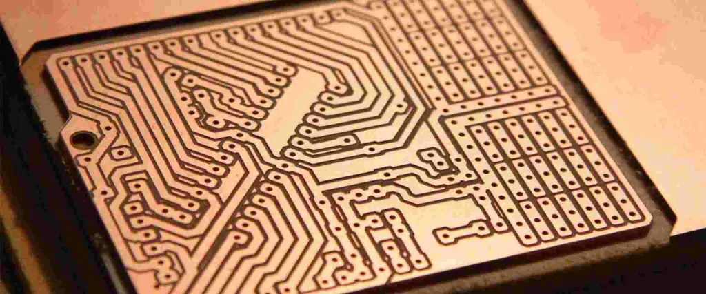
5. Etching
Unwanted copper is removed through chemical etching, leaving only the desired circuit pattern.
6. Solder Mask Application
This is where the matte black PCB process differs significantly. A specially formulated black solder mask is applied to the board.
7. Curing
The board is cured, usually through heat treatment, to set the matte black solder mask.
8. Surface Finish
A surface finish is applied to protect exposed copper and facilitate soldering.
9. Silkscreen
If required, a silkscreen layer is added, usually in white or other light colors for contrast.
Comparison: Matte Black vs. Traditional PCBs
Let’s compare matte black PCBs with traditional PCB colors across various parameters:
| Parameter |
Matte Black PCBs |
Traditional PCBs (e.g., Green) |
| Aesthetic Appeal |
High |
Moderate |
| Heat Dissipation |
Better |
Good |
| Light Reflection |
Low |
Moderate to High |
| Assembly Contrast |
Excellent |
Good |
| Visual Security |
High |
Moderate |
| Cost |
Slightly Higher |
Standard |
| Availability |
Limited |
Widely Available |
| Tradition/Familiarity |
New, Less Common |
Well-established |
Challenges and Considerations
While matte black PCBs offer numerous advantages, there are some challenges and considerations to keep in mind:
1. Cost
The specialized solder mask and potentially lower production volumes can make matte black PCBs slightly more expensive than traditional options.
2. Availability
Not all PCB manufacturers offer matte black as a standard option, which might limit sourcing choices.
3. Inspection Challenges
The dark color can make visual inspection more challenging in some cases, particularly for solder joint quality assessment.
4. Heat Considerations
While black surfaces can emit heat more effectively, they also absorb more heat. This dual nature needs to be considered in thermal design.
5. Novelty Factor
As a relatively new option, there’s less long-term data on the performance and durability of matte black PCBs in various applications.
Future Trends
The popularity of matte black PCBs is part of a broader trend towards more aesthetically pleasing and functionally diverse circuit board options. We can expect to see:
- More color options with specialized properties
- Advanced surface treatments for enhanced performance
- Integration of aesthetic considerations into early-stage PCB design
- Development of eco-friendly PCB materials and processes
Conclusion
Matte black PCBs represent an exciting development in the world of electronics manufacturing. They offer a unique combination of aesthetic appeal and functional benefits, making them an attractive option for a wide range of applications. While they come with some challenges and considerations, their growing popularity suggests that matte black PCBs are more than just a passing trend.
As with any technological choice, the decision to use matte black PCBs should be based on a careful consideration of the specific requirements of each project. Whether for their sleek appearance, thermal properties, or reduced reflectivity, matte black PCBs are certainly leaving their mark on the electronics industry.
FAQ
1. Are matte black PCBs more expensive than traditional PCBs?
Matte black PCBs can be slightly more expensive than traditional PCBs due to the specialized solder mask and potentially lower production volumes. However, the price difference is often minimal, especially for larger orders.
2. Do matte black PCBs affect the electrical performance of the circuit?
Generally, the color of the PCB does not significantly affect its electrical performance. The matte black finish is primarily a cosmetic and functional surface treatment that doesn’t interfere with the circuit’s operation.
3. Can all PCB designs be manufactured in matte black?
In theory, most PCB designs can be manufactured in matte black. However, some very complex or specialized designs might require specific considerations. It’s always best to consult with your PCB manufacturer about the feasibility of using a matte black finish for your specific design.
4. Are matte black PCBs more heat-resistant than traditional PCBs?
While the black color can help with heat dissipation through better emission, it doesn’t necessarily make the PCB more heat-resistant. The heat resistance of a PCB is primarily determined by its base material and overall design, not its color.
5. Can I use regular white silkscreen on a matte black PCB?
Yes, white silkscreen can be used on matte black PCBs and often provides excellent contrast for labels and markings. However, other light colors can also be used effectively, depending on the specific aesthetic and functional requirements of your design.