Why Assembly Testing is Crucial in Electronics Production

Assembly Testing

As technology keeps advancing, there is more demand for testing. Assembly testing plays a crucial role in PCB and electronics manufacturing. Also, this testing is critical within manufacturing processes. This is because it saves time and money. Assembly testing is beneficial to both OEMs and CMs.

Asides assembly testing, there are other forms of testing. In this article, we will be discussing assembly testing, unit testing, and regression testing. Also, we will shed more light on the impact of these tests in production processes.

What is Assembly Testing?

Assembly testing verifies if two or more modules can communicate and generate expected outcomes or not. There is no unit that can carry out stand alone activities. Also, another moduleโ€™s output may be utilized as input by another module. Therefore, it is very crucial if related modules can connect and generate the desired outcome.

You can carry out assembly testing through the UI. Also, assembly testing helps to know if the modules can interact in a proper manner. It is a black box testing style. Assembly testing comprises a complete application which evaluates if a program responds to elementary input. It then shuts the program back.

The brain behind assembly testing is that devices should perform well. Assembly testing shows the interactions among modules in a proper manner defined in the functional requirements by clients.

What is Assembly Integration and Testing?

Assembly integration and testing (AIT) is very crucial. This stage of testing consists of the assembly of components before aligning and testing the optical system. Integration deals with the assembly subsystems and opto-mechanical systems. Also, it carries out glass-metal and metal-metal bonding operations. ย 

Also, integration is a crucial stage in any project. It involves the assembly of components before aligning and testing the system. AIT plays significant roles in certain applications like aerospace. This is because this testing enables the assembly, integration, and testing of a device in a cost-effective way. Overtime, assembly integration and testing has continued to gain momentum in several industries.

AIT guarantees system quality. Also, it ensures the success of a particular project. Assembly integration and testing is widely used in several industries. Costly electronic equipment with complex manufacturing processes requires precision. AIT offers the precision and preparation required for this production process.

The Importance of Independent Assembly Testing

It is important to know how different materials and products will react when integrated. Therefore, assembly testing is a crucial process that identifies how products react when combined. An independent assembly testing provides information on the reaction of some materials. Also, assembly testing is important in formulating an accurate expense budget for a project.

For instance, some industries depend on the reports from assembly testing to meet a learning curve. There are increasing changes in products. Therefore, it is important to study the performance of new products. Also, assembly testing provides industries a trusted source of standard results.

Independent assembly testing offers the best solution in a project. This is because it offers unbiased results. Opting for an independent assembly testing service is the best way to trust the results.  Also, assembly testing assures contract manufacturers their products are of quality standards.

What is Unit Testing?

Unit testing ensures that the program unit meets their requirements. Also, a programmer conducts unit testing. This programmer must be under the supervision of the project team lead. The essence of unit testing is to test every unit individually and in isolation. The programmer achieves this by knowing the expected outputs and inputs to the unit.  

Unit testing is also known as component testing. This testing usually occurs in the implementation stage of a project. However, unit testing isnโ€™t restricted to a function or component. Therefore, the approach determines the definition of unit testing.

Also, the main objective of unit testing is to test if a certain unit of a program meets the expected output when there is a certain input. The programmer needs to beware of the code of the system and the internal logic. Unit testing is a method of carrying out the white box testing. Also, this testing involves verifying the implementation of every specified feature in the โ€œComponent Design.โ€

Examples of unit testing include logic testing for algorithms. Some projects feature critical algorithms. For instance, security implementation and custom setting. Therefore, you can test logic independently. Unit testing can be a simple function or method in case of functional programming.

What is Regression Testing?

Regression testing is a software testing that checks any update or modification in a software. It does this without impacting the working functionality of the particular software. Also, this testing is necessary when there is a code modification in a software.

This testing ensures that the change doesnโ€™t generate bugs in the functioning of the software. Functionality testing of the build begins after clearing regression testing. Also, it verifies that a recent code change doesnโ€™t adversely impact existing features. Therefore, it ensures that new code changes shouldnโ€™t negatively affect existing functionalities.

To carry out this testing, the programmer must debug the code first. Debugging helps to detect the bugs. Once you detect the bugs, the required changes will fix it. After this, the programmer selects relevant cases from the test suite. Regression testing helps to ensure that an application performs properly.

Frequently Asked Questions

What is the difference between Unit testing, Assembly testing, and Regression testing?

Unit testing tests if a certain unit of a program meets the expected output when there is a certain input. A โ€œunitโ€ in this testing refers to a module self contained.

Assembly testing is a step ahead of unit testing. This testing verifies if modules can interact and generate expected outcomes or not. In assembly testing, no unit can carry out stand alone activities.

Regression testing ensures the code change doesnโ€™t generate bugs in the functioning of the software. Functionality testing of the build begins after clearing this testing. Also, it verifies that a recent code change doesnโ€™t adversely impact existing features.

Who should use assembly tests?

Assembly tests are widely used across different industries. These tests offer a lot of advantages to users. An assembly test is ideal for use in designing spacecraft and satellites. Therefore, this test plays significant roles in the aerospace and defense sector.

This test is ideal for identifying the root cause of a device failure. Therefore, this test is suitable for use in industries that need to test their products. Also, assembly tests are widely used by original equipment manufacturers and contract manufacturers.

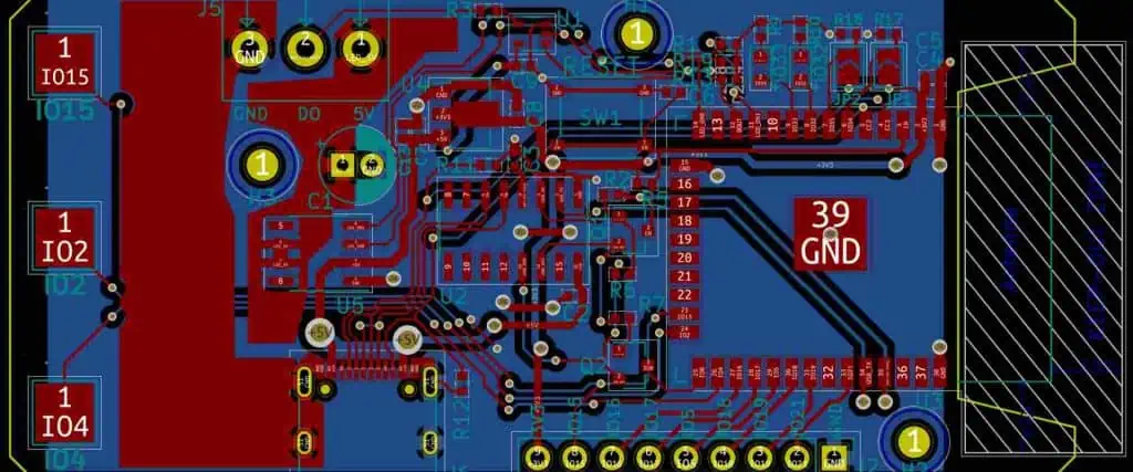
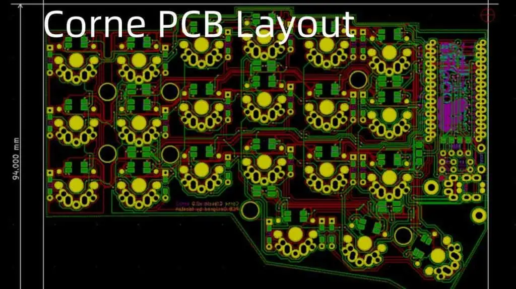
What is Component and PCB assembly Testing?

There is an increasing demand for electronic component testing and verification. Component verification and testing determines component functionality or failure analysis. PCB assembly testing helps to detect and prevent any PCB manufacturing defects.

Testing is important to ensure the fabrication of high quality PCBs. Therefore, all PCB assembly should go through proper testing.

Conclusion

Defective products have costly implications. Therefore, it is important to save time and cost by carrying out the necessary tests. In PCB fabrication and electronic manufacturing, assembly testing is of great importance. We have discussed assembly testing and other forms of testing in this article. Also, we have shed more light on unit testing and regression testing.

Is A FPGA a CPU?

LGA PGA BGA

Field Programmable Gate Arrays (FPGAs) and Central Processing Units (CPUs) are two fundamental components used in many digital systems. But there are some key differences between their architectures and applications. This article will examine if an FPGA can be considered a type of CPU or if they are distinct technologies.

CPU Overview

A Central Processing Unit, or processor, is a digital circuit that executes instructions contained in software programs. CPUs implement fundamental computing operations like:

  • Fetching instructions and data from memory
  • Decoding instructions
  • Executing arithmetic, logic and data processing operations
  • Controlling program flow
  • Communicating with peripheral devices

Modern CPUs utilize architectures like x86, ARM, RISC-V etc. They are fabricated as complex integrated circuits containing billions of transistors. CPUs are optimized for executing sequential instruction streams at high speed.

Key characteristics of CPUs:

  • Fixed architecture optimized for general-purpose code execution
  • Sequential Fetch-Decode-Execute cycle
  • Caches, pipelines, branch prediction for performance
  • Standard interfaces like memory, PCIe, USB
  • Run software operating systems and applications
  • Fabricated by silicon vendors like Intel, AMD, etc.

FPGA Overview

Achronix FPGA

A Field Programmable Gate Array is an integrated circuit containing configurable logic blocks and programmable interconnects. Users can customize the FPGA to implement digital logic functions by programming it after manufacturing.

Capabilities of FPGAs include:

  • Custom logic using Look-Up Tables (LUTs) and flip-flops
  • Flexible I/O interfaces
  • Low-latency parallel execution
  • High bandwidth internal routing
  • DSP slices and block RAM
  • Reconfigurability and field updates

Key characteristics:

  • Programmable logic cells and routing
  • Parallel execution architecture
  • No fixed instruction set
  • Designs defined using HDL or schematic entry
  • Used for hardware acceleration, prototyping, DSP
  • Provided by vendors like Xilinx, Intel (Altera)

So in summary, the CPU is optimized for software programmability while the FPGA is optimized for hardware flexibility and customizability.

Comparing CPUs and FPGAs

Here is a comparison between some key attributes of CPUs and FPGAs:

ParameterCPUFPGA
ArchitectureFixedConfigurable logic + routing
ExecutionSequentialParallel
ProgrammingSoftware instructionsHDL or schematics
PerformanceGeneralized computingApplication-specific acceleration
FlexibilityMinimalHighly flexible
Power efficiencyLowerHigher
CostLowHigh
Design effortLowHigh

While CPUs and FPGAs both implement digital logic functions, they have fundamental differences in capabilities and use cases. CPUs are best suited for running software programs while FPGAs excel at application-specific hardware acceleration.

Can FPGAs Function like CPUs?

CPU PCB

Even though they have different architectures, FPGAs can be configured to implement functionality quite similar to CPUs. This is achieved by programming the FPGA fabric using HDL code to realize components like:

  • Instruction register and decoder
  • Arithmetic logic unit (ALU)
  • General purpose registers
  • Control unit implementing a state machine
  • Caches for instructions and data
  • Bus interfaces like AXI, OCP, etc.

Using these CPU-like blocks, FPGAs can execute software binary code loaded into their internal memory and access external memories and peripherals.

While possible, such soft CPU architectures on FPGAs have lower performance compared to hard CPUs built as ASICs. They consume more power and area when implemented in programmable logic. Hence FPGAs are not a replacement for CPUs in running software.

Can CPUs be Used like FPGAs?

Modern CPUs also have some capabilities to improve flexibility and customizability typically associated with FPGAs:

Reconfigurable Instruction Sets

RISC-V, ARM and other latest CPU architectures have configurable instruction sets that can be extended with custom logic and accelerators.

Partial Reconfiguration

Features like Intel Management Engine allow parts of a CPU to be reconfigured without affecting the entire device.

FPGA Co-Processors

Intel and AMD CPUs integrate FPGA fabric as co-processors to enable application specific acceleration.

General Matrix Multiply Units

Programmable matrix multiply units in CPUs like Intel DL Boost provide an FPGA-like configurability.

However, these capabilities are quite limited compared to full-fledged FPGAs. The CPU flexible logic is tightly coupled to fixed cores and cannot be repurposed independently. CPUs are still firmly in the software programmability domain versus FPGAs designed for custom hardware flexibility.

Reasons FPGAs Are Not CPUs

While FPGAs can implement soft CPU cores, they differ from true CPUs in several fundamental aspects:

Sequential vs Parallel Execution

The Von Neumann architecture used in CPUs is optimized for sequential fetch-decode-execute. FPGAs employ a parallel architecture executing custom hardware blocks concurrently.

Fixed vs Configurable

CPUs have standardized fixed blocks like ALUs, caches, etc. In contrast, FPGAs are fully customizable at the logic and routing level.

Hardware vs Software Programming

CPUs execute software instructions. FPGAs are programmed using hardware description languages (HDLs) defining digital logic.

General Purpose vs Application Specific

CPUs are generalized computing engines. FPGAs are designed and optimized for a specific application.

Discrete Chips vs On-Chip Variants

Standard CPUs are manufactured as standalone chips. FPGAs are on-chip accelerators integrated with CPUs.

Due to these architectural differences, even though both implement digital logic, FPGAs cannot be classified as general-purpose CPUs. They complement CPUs with application-specific acceleration.

Reasons CPUs Are Not FPGAs

Intel FPGA

While CPUs are gaining more configurable logic, they are fundamentally not equivalent to FPGAs due to the following:

Instruction Driven vs Digital Logic

CPUs are constrained to an instruction set architecture. FPGAs allow designers to implement arbitrary digital logic unconstrained by instructions.

Limited Flexibility vs Highly Programmable

CPU configurable logic is minimal compared to the highly programmable FPGA fabric with millions of logic cells and robust routing.

Fixed Pipelines vs Arbitrary Datapaths

The CPU datapath is fixed. FPGAs can implement any custom datapath.

Full-Stack Software vs HDL Based Development

CPUs utilize rich full-stack software ecosystems. FPGA design relies on hardware description languages.

Generalized Cores vs Specialized IP

CPUs cores are generalized processors. FPGAs integrate application-specific accelerators and interfaces.

Due to these inherent differences, CPUs cannot match the custom hardware flexibility and parallelism offered by FPGAs.

Similarities Between FPGAs and CPUs

While they have distinct architectures and applications, FPGAs and CPUs have some high-level similarities:

  • Both implement digital logic functions ultimately consisting of logic gates and flip flops at their foundation.
  • They utilize similar semiconductor fabrication techniques like CMOS on silicon wafers.
  • Standard CAD tools are used for designing and verifying both FPGA and CPU chips.
  • They employ common interfaces like PCIe, DDRx memory, USB, etc. to communicate with peripherals.
  • Higher level system integration happens over standard buses like AXI, OCP, Avalon, etc.
  • They are combined together frequently as FPGA accelerated CPUs or SoC designs.

So while distinct internally, from an external perspective FPGAs and CPUs enable complementary benefits for digital systems designers.

Pros and Cons of FPGAs Compared to CPUs

FPGAs Advantages Over CPUs

  • Customizable and reconfigurable logic
  • Massive parallelism
  • Optimized for application-specific needs
  • Low latency, high bandwidth
  • Algorithms directly in hardware
  • Energy and performance efficiency
  • Flexibility for future enhancements

FPGAs Disadvantages Relative to CPUs

  • Higher design complexity
  • Specialized toolset and skillset
  • Redesign needed for new algorithms
  • Limited by available gates
  • Difficult optimization and debugging
  • Higher cost
  • Not software programmable

CPU Advantages Over FPGAs

  • Generalized architecture
  • Mature software ecosystem
  • Easy integration and abstraction
  • Quick to develop and modify
  • Scalable through multicore
  • Broad availability of standard CPUs

CPU Disadvantages Relative to FPGAs

  • Less performance and power optimized
  • Higher latency
  • Limited parallelism
  • Constrained by instruction set
  • Not tailored for applications
  • Less flexible for future enhancement

In summary, both technologies have pros and cons depending on the use case requirements, so they complement each other in building high performance digital systems.

Conclusion

While FPGAs and CPUs both provide digital logic capabilities, they have fundamentally different architectures optimized for their specific applications. CPUs are designed to efficiently execute software instruction streams. In contrast, FPGAs offer flexible digital logic that can be customized to accelerate specific workloads. FPGAs do not have a fixed instruction set or run software operating systems and are programmed using hardware description languages rather than a software toolchain. While FPGAs can implement soft CPU cores, they lack the full software programmability of a microprocessor. Similarly, CPUs are gaining more configurable logic but cannot match the hardware customizability of FPGAs. Both technologies have complementary strengths ideal for heterogeneous computing systems.

Top 5 FAQs about FPGAs and CPUs

Xilinx Kintex fpga
Xilinx Kintex fpga

Here are answers to some frequently asked questions about the relationship between FPGAs and CPUs:

Q1: Can an FPGA fully replace a CPU in a system?

A: Not usually, because FPGAs lack native software programmability. FPGAs excel at accelerating fixed hardware functions but CPUs are still needed to run software programs controlling the overall system.

Q2: Do FPGAs implement the same functions as a CPU internally?

A: No, FPGAs consist of configurable logic/routing while CPUs have fixed functional blocks like ALUs, caches, pipelines. The internal architecture is fundamentally different.

Q3: Can CPUs implement the same functionality as FPGAs?

A: To a limited degree, but CPUs have very constrained configurable logic compared to the massive programmable fabric in FPGAs. CPUs cannot match FPGA customizability.

Q4: Why can’t FPGAs fully replace CPUs if they can also execute software?

A: Soft processor cores in FPGAs have much lower performance than hard CPU cores. FPGAs lack native software programmability and OS support required in most systems.

Q5: Will FPGAs ultimately replace CPUs as technology improves?

A: Unlikely, since CPUs excel at generalized software execution which is easier to develop for. FPGAs and CPUs will continue to complement each other in heterogeneous compute systems.

In summary, while FPGAs and CPUs overlap in some capabilities, they are optimized for different applications and provide complementary strengths that make them both indispensable for modern digital designs.

How to Design Your Own FPGA ?

fpga design

Field Programmable Gate Arrays (FPGAs) are integrated circuits that can be programmed and reconfigured by the user after manufacturing. This makes them a flexible and powerful option for digital circuit implementation. While hobbyists typically use commercial FPGAs from vendors like Xilinx and Intel (Altera), it is possible to design your own FPGA as well. This article will provide an overview of the key steps involved in custom FPGA design.

Overview of FPGA Architecture

To understand how to design an FPGA, we first need to understand the high-level architecture. A basic FPGA consists of the following key components:

Configurable Logic Blocks (CLBs) โ€“ These are the basic logic units whose functions can be programmed. CLBs include lookup tables (LUTs) and flip-flops.

Programmable Interconnects โ€“ Routing channels between CLBs can be programmed to connect them in different ways. This includes connection boxes and switch matrices.

I/O Blocks โ€“ Provide the interface between the I/O pins and internal programmable logic. Support various I/O standards.

Clock Circuitry โ€“ Includes clock buffers, PLLs, DLLs to drive clock networks across the FPGA.

Memory and DSP Blocks โ€“ Some FPGAs include dedicated blocks of RAM, ROM and DSP slices.

Configuration Memory โ€“ Stores the programming that defines the FPGA functionality. Volatile or non-volatile.

PCIe, Ethernet, etc. โ€“ Some FPGAs have hard cores for various interfaces integrated on-chip.

Processor Cores โ€“ Modern FPGAs may include embedded ARM cores for SoC applications.

This architecture with flexible programmable logic, routing and I/O provides the foundation for an FPGA that can be customized by designers.

FPGA Design Flow Overview

FPGA processor

Designing an FPGA from scratch involves several steps that can be grouped into two main phases:

1. Design and Verification

This involves using HDLs like VHDL or Verilog to design, simulate and verify the functionality of the various FPGA blocks at the register-transfer level (RTL). EDA tools like Quartus from Intel or Vivado from Xilinx are leveraged for synthesis and simulation. Reusable IP cores may be purchased for some functions.

Once RTL models of the FPGA fabric are finalized, gate level netlists are generated, checked for logical equivalence against RTL and timing analysis is done to meet speed goals.

2. Physical Implementation

The gate level netlist is then taken through the physical design stages of floorplanning, place-and-route, timing closure, and tapeout. Electronic design automation (EDA) tools automate mapping the netlist to actual gates and transistors on silicon but manual optimization is required.

The final tapeout is the complete database (GDSII stream format) defining the photolithographic masks to manufacture the FPGA. This is sent to a silicon foundry like TSMC for fabrication.

This overall flow requires expertise in digital logic design, HDL modeling, ASIC/FPGA architecture and semiconductor fabrication. Let’s look at each major step in more detail.

Detailed FPGA Design Steps

Here are the specifics of designing and implementing an FPGA from concept to final silicon:

1. Concept Development

  • Define target device capabilities and applications. Factors like logic cells, speed, power, cost, and features impact architecture decisions.
  • Specify high-level functional requirements. Example: “The FPGA should support 250K logic cells, 200 MHz speed and DDR3 memory interface”.
  • Plan top-level architecture – logic blocks, routing channels, I/O count, clocking, embedded IP cores etc.
  • Evaluate commercial IP cores that can be licensed to reduce design effort for standard functions.

2. Feasibility Study

  • Research existing open literature and patents around similar architectures.
  • Create silicon area and power rough estimates for planned architecture.
  • Estimate expected timing performance based on planned process node.
  • Assess if performance targets can realistically be met within area and power budget.
  • Refine architecture if needed based on feasibility study results.

3. RTL Functional Design

  • Use Hardware Description Languages like VHDL or Verilog to model the following FPGA modules at the RTL level:
    • Configurable Logic Blocks (CLBs)
    • Input/Output Blocks (IOBs)
    • Programmable Interconnect
    • Clocking resources
    • Memory/DSP blocks
    • Configuration memory
    • Any other logic blocks
  • Verify functionality by simulating RTL modules/subsystems. Develop testbenches to validate operation.
  • Iterate modules as needed till functionally correct.

4. Synthesis and Gate-Level Simulations

  • Perform logic synthesis to convert RTL models into technology-mapped gate-level netlists.
  • Verify netlists match RTL functional behavior via gate-level simulation.
  • Run equivalency checking to formally verify logical equivalence of netlists vs RTL code.
  • Iterate until netlists match RTL functionality and are logically equivalent.

5. Static Timing Analysis

  • Perform static timing analysis on gate-level netlist using timing constraints.
  • Identify critical timing paths that need optimization to meet clock frequency target.
  • Modify RTL and re-synthesize to close timing if needed.
  • Sign-off on timing closure when all paths meet timing goals with margin.

6. Floorplanning

  • Determine the relative placement of FPGA blocks on the die based on connectivity and shape.
  • Decide aspect ratio and pin locations.
  • Allocate space for routing channels between blocks.
  • Ensure good floorplan to optimize timing, routability and die area.

7. Power Planning

  • Estimate power consumption of logic blocks and I/Os.
  • Plan power grid distribution across the die to provide clean power to cells.
  • Insert power gating cells or switches if needed to control power.
  • Add voltage islands if required for low power modes.

8. Place and Route

  • Automatically place logic gates and cells within each FPGA functional block.
  • Route interconnect wires between cells following electrical and timing constraints.
  • Verify all connections meet physical design rules for width/spacing.
  • Iterate optimizations to meet timing closure and minimize wirelength.

9. Physical Verification

  • Run design rule checks for errors like minimum spacing or overlaps between shapes and layers.
  • Verify layout versus schematic matching.
  • Extract parasitics and redo timing analysis to validate performance.
  • Perform formal verification on final routed layout.
  • Signoff physical verification when the tapeout database passes all checks.

10. Tapeout

  • Generate final GDSII layout database containing mask layers to send for fabrication.
  • Include other deliverables like LEF, Liberty timing models, CDL netlist, etc.
  • Perform manufacturability checks like DFM analysis.
  • Submit tapeout data to foundry like TSMC for mass production.

With these steps complete, the FPGA design is fabriccated into actual silicon chips that can be programmed by designers!

Challenges in Custom FPGA Design

Achronix FPGA

While the design flow seems straightforward, creating a custom FPGA from scratch poses several tough challenges:

  • Achieving timing closure across P&R, synthesis and physical optimization is extremely difficult given the complexity.
  • Router has to implement programmable interconnects with an enormous solution space.
  • Strict silicon area targets for optimal transistor density and die yield.
  • Power grid has to provide very clean power across the die.
  • Thorough simulation and verification requires exhaustive testbenches.
  • Fabrication process tolerances can affect performance.
  • Requires large, experienced, multi-disciplinary engineering teams.
  • Total design cost can easily reach tens of millions of dollars.

Because of these challenges, custom FPGA startups require substantial financial backing to design competitive products. Leveraging existing FPGA vendor solutions or licensing their IP can help mitigate technical risks and costs.

When Does Custom FPGA Design Make Sense?

Given the high costs, effort and risks involved, developing a custom FPGA device from scratch is only justified for a few specific applications:

  • Building differentiated FPGA products for a niche application space not served well by existing vendors. Eg. radiation-hardened FPGAs.
  • Merging an FPGA with other silicon IPs like processors, SerDes, analog, etc. to create a highly integrated system-on-chip solution.
  • Implementing novel FPGA architectures for research purposes to push new ideas in academia.
  • Developing strategic advantage in critical domains like aerospace, defense or high-end computing where competitive edge in programmable chips is valued.

For most commercial applications, licensing proven FPGA technology from Xilinx, Intel or others and customizing the design on top offers a faster time-to-market with lower risk.

Options for FPGA Design Without Fabricating Silicon

For hobbyists, researchers, or smaller teams with limited budgets, there are options to design and validate custom FPGA architectures without having to actually fabricate the chip which requires millions of dollars:

FPGA Prototyping Boards

  • Prototyping boards like the Xilinx Virtex-7 or Intel (Altera) Stratix-10 allow implementing and testing FPGA architectures using their programmable fabric.

FPGA Emulation on FPGAs

  • Using HLS or HDLs, the architecture of a novel FPGA can be modeled and functionally verified by mapping it onto an existing physical FPGA.

FPGA Simulation Environments

  • Computer-based simulations of FPGA fabrics using HDL testbenches and tools like ModelSim can be created to evaluate new architectures.

Rapid Prototyping Using CPLDs

  • For limited logic capacity testing, Complex Programmable Logic Devices (CPLDs) provide an easier and cheaper alternative to prototype concepts.

Cloud-based FPGA Resources

  • Xilinx and Intel provide cloud-based access to FPGAs that can be leveraged for experiments before committing to silicon fabrication.

While not exactly the same as taping out real custom silicon, these options allow flexibility for innovators and startups to validate their ideas without prohibitive fab costs.

Open Source FPGA Projects

fpga design

For reference, there are some open-source projects that aim to provide free and customizable FPGA platforms:

  • Symbiflow – Toolchain for developing open-source FPGAs.
  • LiteX – Migen and LiteX ecosystem for building FPGA-based systems.
  • OpenFPGA – Open-source framework for developing FPGA architectures.
  • GreenArrays – Ultra low-power open FPGA architecture.
  • Kiwi – Educational miniature FPGA board designed in New Zealand.

While full-custom FPGA design requires substantial expertise and effort, these open initiatives help democratize access to FPGA technology for hobbyists.

Conclusion

Designing a custom FPGA device from the ground up is a complex process requiring advanced engineering expertise across RTL design, EDA tools, architecture, physical implementation, and fabrication. While challenging, for specific applications like IP differentiation, research or vertical integration, a custom-designed FPGA can provide strategic benefits. For most purposes, however, leveraging existing proven FPGA technology and IP from vendors like Xilinx and Intel provide the best trade-offs. The emergence of open-source FPGA tooling and platforms is also making FPGA customization more accessible to innovators.

Top 5 FAQs about FPGA Design

Here are some frequently asked questions about designing your own custom FPGA:

Q1: What expertise is required for full-custom FPGA design?

A: You need digital design engineers proficient in RTL coding (VHDL/Verilog), FPGA architects, physical design engineers, verification specialists, and semiconductor process technology know-how.

Q2: What kind of budget is needed for a new FPGA tapeout?

A: The cost can range from $10M to $50M+ for a new full-custom FPGA depending on the complexity, process node, tool licenses, engineering team size etc.

Q3: How long does it take to design and tapeout an FPGA?

A: For a reasonably complex FPGA architecture with all the steps done rigorously, the entire process typically takes 12-18 months from concept to final tapeout database.

Q4: Can I modify an existing FPGA without taping out new silicon?

A: Yes, you can customize existing FPGA designs using HDL overrides, IP integration, partial reconfiguration etc. without having to create a brand new device from scratch.

Q5: Is open source FPGA technology mature enough for commercial use?

A: Open-source FPGA tooling provides a great learning platform but still has limitations in the complexity of designs possible compared to Cadence/Synopsys/Mentor commercial EDA tools.

What is Altera quartus used for?

Altera QUARTUS

Overview of Altera Quartus

Altera Quartus is a design software produced by Intel (formerly Altera) for programmable logic devices. It allows engineers to design, analyze, optimize, and program Intel FPGAs, CPLDs, and SoCs using system-level design techniques and advanced place-and-route algorithms.

Some key capabilities offered by Altera Quartus:

  • FPGA design entry using schematic, HDL, block diagrams
  • Timing analysis, power analysis, design optimization
  • IP core integration, parameterization
  • Advanced place-and-route algorithms
  • Device programming and configuration
  • System-level integration and co-simulation
  • Support for Intel and third-party tools/IP

Altera Quartus works across the entire Intel FPGA product range and provides a unified environment for FPGA and SoC development. It includes tools for the complete development cycle from design to test, programming and debug.

The Quartus software runs on Windows and Linux operating systems. A free version is available for small FPGAs with limited features.

Key Features of Altera Quartus

Here are some of the major features provided by the Altera Quartus suite:

Design Entry

  • VHDL, Verilog, SystemVerilog support for RTL design
  • Schematic capture editor
  • Block diagram design with memory mapped interconnect
  • Import from math software like MATLAB/Simulink

Simulation and Verification

  • RTL simulation engine for functional verification
  • Timing analysis for design optimization
  • Power analysis for low-power designs
  • SignalTap logic analyzer
  • Formal verification support

Synthesis and Place-and-Route

  • Advanced synthesis optimizes for speed, area or power
  • Physical synthesis optimizes post-layout netlist
  • Timing-driven incremental place and route
  • Support for automated optimization strategies
  • Floorplan editor for constraint-driven layout

Program and Debug

  • Program Intel FPGA devices via programmer
  • In-system source-level debugging
  • Signal probe to tap internal signals
  • Device configuration via PCIe, Ethernet, JTAG

IP Library and Third-party Integration

  • Extensive library of Intel FPGA IP cores
  • Parameterizable IP core generation
  • Third-party tool integration e.g. MATLAB, Synopsys
  • Co-simulation with various simulators
  • Support for industry standard interfaces

Applications and Use Cases

Altera Quartus can be used across a wide spectrum of applications that utilize programmable logic chips. Here are some common use cases:

Prototyping and Pre-Silicon Validation

Quartus allows quick prototyping of system architectures on FPGAs for early validation before ASIC designs are finalized. Reduces risk by proving the design before manufacturing.

Networking and Telecom

Used for implementing algorithms in networking gear like switches, routers, base stations, transmission systems etc. Provides rapid upgrades via reprogramming.

IoT and Embedded Systems

Ideal for implementing logic in smart sensors, industrial controls, motor drives, automation systems etc. that require flexibility.

Automotive

Used to design engine control units, driver assistance systems, infotainment systems etc. which require reliability and safety.

Aerospace and Defense

Suitable for mission critical guidance systems, navigation electronics, signal processing etc. that demand precision.

High-Performance Computing

HPC applications leverage FPGAs for parallel processing. Used in data centers, supercomputers, artificial intelligence.

SoC Design

Quartus supports embedded ARM cores for designing entire systems on a programmable chip.

Academic Research

Widely used in universities and research centers due to low cost, flexibility and rich feature set.

In summary, Altera Quartus serves any application that benefits from FPGA capabilities like rapid prototyping, hardware acceleration, low latency, power efficiency etc.

Quartus Editions – Comparison of Features

Intel offers different editions of Altera Quartus based on the FPGA model size and features required. The key variants are:

Quartus Prime Lite

  • Entry-level design for low-end FPGAs
  • Limited to small designs
  • Only supports Verilog/VHDL
  • No advanced analysis or debug
  • Free edition for Intel MAX series

Quartus Prime Standard

  • For mid-range FPGAs like Cyclone series
  • Full HDL support with advanced synthesis
  • Timing/power analyzer, SignalTap logic analyzer
  • Supports Device Programming
  • Costs around $2,500 per year

Quartus Prime Pro

  • Highest performance FPGAs like Stratix/Arria
  • Advanced place-and-route algorithms
  • Floorplan Editor, PowerPlay power analyzer
  • Formal verification, design security features
  • Subscription around $5,500 per year

SoC Embedded Design Suite

  • All Quartus Prime Pro features
  • Multi-core design with ARM cores
  • Platform Designer system integration
  • Nios II embedded processor design
  • Subscription – $9,000 per year

So developers can choose the edition with capabilities matching their design requirements. Entry-level projects can leverage the free version whereas complex designs require advanced features of Pro or SoC editions.

How to Choose the Right Edition?

Here are some key considerations when selecting the Quartus edition for your project:

FPGA Model

Pick an edition that supports your target FPGA architecture – MAX, Cyclone, Stratix etc. Entry editions have FPGA size limits.

Design Complexity

Higher complexity needs more advanced place-and-route, analysis and debug features only available in Pro/SoC.

Design Methodology

System-level, visual designers benefit from Embedded/SoC edition capabilities. RTL designers can stick to Standard or Pro.

Tool Integration Needs

Projects needing to integrate MATLAB, C/C++ and verification tools require Pro or Embedded editions.

Budget

Free and Standard editions are ideal for academic and hobbyists. Commercial users should evaluate the design productivity benefit of the premium editions.

Technical Support

Paid editions include Intel technical support which can be useful for mission-critical projects. Free and academic editions have community forums only.

For most hobbyists and engineering students, the free Quartus Lite provides an abundant feature set. Enterprise users require the premium editions to access Intel’s latest architectures, place-and-route innovations and technical support.

Typical FPGA Design Flow Using Quartus

Here is a typical FPGA design flow using the Altera Quartus suite:

  1. Design Entry – Use schematic entry, VHDL/Verilog coding or block diagrams to define the RTL or system-level design.
  2. Functional Simulation – Verify functionality by simulating the design in ModelSim integrated with Quartus.
  3. Synthesis – Synthesize the RTL to convert to logic gates. The Compiler optimizes for speed, area or power.
  4. Place-and-Route – Place logic blocks and route signal connections using timing-driven algorithms to meet design constraints.
  5. Timing Analysis – Verify timing performance to ensure clock frequency requirements are met. Optimize critical paths as needed.
  6. Power Analysis – Estimate power consumption and optimize power saving options like clock gating.
  7. Programming – Configure the FPGA by programming it with the compiled design files via programmer.
  8. Debug – Debug the design on the development board via SignalProbe, SignalTap or Logic Analyzer.
  9. Timing Closure – Iterate between place-and-route, timing analysis and optimization until timing goals are met.

With these steps, designers can implement their digital systems on Intel FPGAs using the Quartus integrated environment.

How is Quartus Different from Xilinx Vivado?

Xilinx Vivado and Altera Quartus serve the same purpose – to design and program FPGAs manufactured by their respective companies. Both provide a unified environment for FPGA development.

Here are some key differences between Quartus and Vivado:

Supported FPGA Vendors

  • Quartus supports Intel (Altera) FPGAs
  • Vivado supports Xilinx FPGAs

Toolset Integration

  • Vivado has tighter integration between analysis, implementation and debug tools
  • Quartus offers broader third-party integrations like MATLAB/Simulink, Synopsys tools

IP Libraries

  • Both have exhaustive IP libraries tailored to their FPGAs
  • Vivado includes embedded ARM cores while Quartus supports Nios soft cores

Programming Interface

  • Vivado provides command line Tcl interface
  • Quartus offers GUI and Qsys system integration tools

Licensing

  • Vivado WebPACK is free for small FPGAs
  • Quartus Prime Lite is free for Intel MAX series

So in essence, the two serve the same purpose but are optimized for their respective FPGA architectures. Users typically prefer using the vendor provided toolchain. But designs can be migrated across platforms with some effort.

Advantages and Disadvantages of Quartus

Here are some of the major pros and cons of using the Altera Quartus suite:

Advantages

  • Unified design environment for Intel FPGAs and SoCs
  • Advanced timing/power analysis and optimization
  • Mature scheduling, placement and routing algorithms
  • Extensive optimization strategies to meet constraints
  • Simulation, debug and programming in one suite
  • Broad support for standards and third-party tools
  • Huge library of Intel FPGA optimized IP cores
  • Effective for both RTL designers and system architects

Disadvantages

  • Only supports Intel/Altera FPGAs
  • Less intuitive compared to GUI-driven Vivado
  • Steeper learning curve than schematic/block design flows
  • Primarily targets RTL designers rather than system architects
  • Limited support for latest high-end EDA standards
  • Can be slow for optimizing large hierarchical designs
  • Expensive licenses for full-featured editions

In summary, Quartus provides a very capable design environment tailored for Intel’s FPGAs but has a learning curve for new users. The free edition is an easy way to get started for Intel-based designs.

Top 5 FAQs about Quartus Lite

Here are some frequently asked questions about using the free Quartus Prime Lite edition:

Q1: What FPGAs are supported in Quartus Lite?

Quartus Lite only supports small FPGAs like the Intel MAX 10 series. Larger devices require Standard or Pro editions.

Q2: Can I simulate my design with Quartus Lite?

Yes, Quartus Lite includes ModelSim-Intel Starter Edition for RTL simulation and functional verification.

Q3: Does Quartus Lite allow timing analysis?

No, Quartus Lite does not have timing analysis, power analysis or formal verification capabilities.

Q4: Can I build a PLL using Quartus Lite?

Unfortunately PLLs are not supported in the free version. You would need Quartus Standard or Pro.

Q5: Is there technical support for Quartus Lite users?

No official support. You would need to rely on community forums and knowledge bases for assistance.

In summary, Quartus Lite has limited capabilities but lets you get started with Intel FPGA design at no cost. It works well for academic projects but commercial users require the Standard or Pro editions.

Is Eagle PCB design software free?

Top PCB design software

An overview of Eagle PCB design software

Eagle (Easily Applicable Graphical Layout Editor) is a popular printed circuit board (PCB) design software package developed by CadSoft and now owned by Autodesk. It allows electronic engineers and enthusiasts to design printed circuit boards and schematics for electronics projects.

Eagle consists of a schematic editor for creating circuit schematics and a PCB layout editor for designing PCBs. It also includes an auto-router module for automatically routing traces on the PCB.

Some key features of Eagle include:

  • Schematic capture with over 7000 parts in component libraries
  • PCB layout and routing
  • Design rule checking to ensure manufacturability
  • Autorouting of PCB traces
  • Gerber and NC drill file generation for manufacturing
  • Import/export of CAD and image files
  • Simulation and 3D modeling

Eagle is available in free and paid versions. The free version has limited board size, number of layers and part libraries but is sufficient for basic projects. The paid versions start at around $500 for a yearly subscription and allow bigger board sizes, more layers and components.

Eagle Free vs Paid

Here is a comparison between the free and paid versions of Eagle:

FeatureEagle FreeEagle StandardEagle Professional
Board size100 x 80 mm160 x 100 mmAny size
Layers2416
Schematic sheets1UnlimitedUnlimited
Library partsLimitedOver 7000Over 7000
AutorouterNoYesYes
PriceFree$55/year$1600/year

So in summary, the free version is great for basic projects but limits board size and layers. The paid versions unlock more features and capabilities.

Is the free version really free to use?

Modular PCB Design
Modular PCB Design

Yes, the free/Lite version of Eagle is completely free to download and use. There are no hidden costs or licensing fees associated with it. The free version is meant to allow hobbyists, students and enthusiasts to get started with PCB design at zero cost.

However, the free version does have some limitations imposed to encourage users to upgrade to the paid versions. As seen earlier, the free Eagle has limited board size (100 x 80 mm), only 2 layers, and a restricted component library. These constraints may be inadequate for more complex projects. But for simple boards, the free version offers full access to schematic capture, layout, autorouting and file generation features.

The free version is licensed for non-commercial use only. Those intending to manufacture and sell boards designed with free Eagle need to purchase a commercial license.

Some key things to note about the free Eagle license:

  • No cost to download, install and use
  • Available for Windows, Mac and Linux
  • Fully functional schematic and layout editors
  • No locked features or disabled tools
  • Can be used to design basic PCBs for hobby and learning
  • Output files can be used for manufacturing with PCB fabrication services
  • Non-commercial license only – commercial use requires paid license

So in summary, the free Eagle provides a very capable design tool at no cost for non-commercial use. It is a great way to get started with PCB design with no financial investment. The feature limits encourage upgrading to paid versions when more complex or commercial boards are required.

What are the steps to download and install the free version?

Downloading and installing the free version of Eagle is quick and straightforward. Here are the steps:

1. Download Eagle from the Autodesk website

Go to the Autodesk Eagle website and click the “FREE DOWNLOAD” button to download the latest free version install file. Choose the version for your Windows, Mac or Linux OS.

2. Run the install file to launch the installation wizard

Locate the downloaded install file and double click to launch the installation process. Follow the setup wizard by clicking Next and accepting the license agreement. Choose the installation folder location.

3. Select the ‘Lite’ installation when prompted

During installation, you will be asked to select between the Free/Lite version or Premium/Standard version. Make sure to select the ‘Lite’ or ‘Free’ option.

4. Allow the installation to complete

Continue with the installation by leaving the default options enabled. The setup will copy Eagle files and install required libraries and device files.

5. Launch Eagle in EAGLE Lite mode

Once installation completes, you can launch Eagle directly. The software will open in the Free/Lite mode with restrictions applicable.

That’s it! With those simple steps you will have the free version of Eagle ready to start designing basic PCB projects.

What are the key limitations of the free version?

esp32 pcb design
esp32 pcb design

While the free Eagle allows unfettered access to the core PCB design features, it does impose some constraints to limit board complexity. Being aware of these limitations will help make best use of the free version.

1. Limited board size

The maximum PCB size is restricted to 100 x 80 mm or about 4 x 3.2 inches. This allows simple and compact boards but rules out bigger designs.

2. Only 2 PCB layers

Designs are constrained to 2 copper layers – top and bottom. High density designs may require 4 or more layers.

3. No auto-routing

The autorouter module is disabled in the free version. Traces will need to be routed manually.

4. Restricted component libraries

The component libraries contain fewer parts compared to the paid versions. If required parts are unavailable, they will need to be created from scratch.

5. Single schematic sheet

Designs are limited to one schematic sheet. Multi-page schematics for complex circuits cannot be done.

6. No technical support

There is no technical support for the free version. You will need to rely on online help resources and communities.

7. Non-commercial use license

Boards designed in free Eagle cannot be used for commercial production and sale.

So in summary, the free Eagle is very capable for basic hobby and learning projects but hits limitations for more advanced PCB designs intended for volume production.

What projects is the free version suitable for?

The free Eagle toolset is well equipped for hobbyist and student projects that require simple PCBs without high complexity. Here are some examples of projects suitable for the free version:

  • Simple microcontroller boards like Arduino shields
  • Basic breakout boards for sensors, motors, connectors etc.
  • Analog circuits like opamp filters, oscillators and amplifiers
  • Power supply circuits using linear regulators and charge controllers
  • LED lighting projects using a few discrete components
  • Prototyping boards like breadboards and perfboards
  • Education and learning focused projects
  • Wireless circuits using modules like Bluetooth, WiFi
  • Non-critical, low-volume or one-off personal projects

For such applications, the free Eagle provides full PCB design capabilities without limitations. Complex commercial projects with higher layer counts, small features and tight tolerances may require the paid version.

Overall, the free Eagle is a great design tool for educational, hobby and basic prototyping applications thanks to its generous non-commercial license.

What are some tips to work around the free limitations?

The generous free capabilities of Eagle allow designing surprisingly complex boards despite the imposed restrictions. Here are some tips to work around the limitations:

Optimize component placement

Careful placement while leaving room for routing helps reduce the need for extra layers. Place connectors, keys and grouped components intelligently.

Use both sides for routing

Effectively utilize both top and bottom copper layers for routing traces. Plan component placement to simplify routing.

Use surface mount devices

SMD parts take less space than through-hole, allowing greater component density.

Utilize Eagle libraries

Make use of the huge selection of readymade schematic symbols and PCB footprints in Eagle’s component libraries.

Break out sections into modules

Partition complex circuits into smaller sub-sections using connectors to interface between modules.

Design hierarchically

Group related schematic sections into hierarchical blocks to reduce clutter.

Create custom libraries

For unavailable parts, build custom schematic and package libraries.

Reduce trace width

Use thinner traces when layout area is constrained.

Share grounds

Use ground planes/polygons instead of drawing individual ground traces.

With smart strategies like these, fairly complex boards can be designed and routed within the free version’s limitations.

What are some good projects for getting started?

Corne PCB Layout
Corne PCB Layout

Eagle’s free version provides an excellent platform for electronics enthusiasts and students to gain experience with PCB design. Here are some recommended beginner-friendly projects:

1. Arduino Shield

Arduino shields are add-on boards that stack onto an Arduino board to expand its capabilities. A custom Arduino shield is a great first project to implement in Eagle.

2. LED Blinkers

A simple circuit with a microcontroller, clock source and a few LEDs makes for an easy first project in Eagle. Useful to gain experience with schematics and layout.

3. Voltage Regulator

Linear voltage regulator designs allow creating a clean and stable power supply source for other circuits. Simple to layout and route.

4. H-Bridge Driver

Used to control motors, H-bridge drivers utilize a few MOSFETs or transistors and passive components. Easy to design and construct.

5. Buck Converter

Switching buck converter circuits efficiently step down voltage levels. Good practice for SMD-based designs.

The open-ended nature of these projects provides flexibility to get comfortable with Eagle’s interface and features at your own pace.

What are some good resources for learning Eagle as a beginner?

Here are some recommendations of resources to help get started with learning PCB design using the free version of Eagle:

Eagle Tutorials

Books

YouTube Tutorials

Great Eagle video tutorials are available on YouTube channels like All About Circuits and Contextual Electronics.

Forums

The Eagle Support Forum at Autodesk and Element14 Community are active in solving issues with Eagle.

With these excellent guides, tutorials, books and an active user community, the free Eagle provides everything you need to get started with PCB design for your own projects.

Top 5 FAQs about Eagle Free

Here are answers to some frequently asked questions about using the free version of Eagle:

Q1: Does the free version expire after some time?

No, there is no expiration date associated with the free Eagle. You can use it indefinitely for free with no time restrictions. Only a paid license is required for commercial use.

Q2: Can I use the AutoRouter with the free version?

Unfortunately no, the AutoRouter module is disabled in the free version and can only be used after buying a paid license.

Q3: Can I design 2-layer boards for commercial production?

PCBs designed with free Eagle cannot be used for commercial purposes due to the non-commercial license. A paid license is required for mass production.

Q4: Does free Eagle allow importing custom libraries?

Yes, you can freely import custom created or downloaded schematic symbols and package libraries into the free version of Eagle.

Q5: Can I unlock more features in the free version?

The free Eagle is deliberately limited in capabilities to motivate purchasing the paid versions. There is no way to unlock features like board size or layers in free Eagle.

So in summary, the free Eagle provides plenty of capability for hobbyist use but paid licenses are required for commercial projects and access to advanced features. The limitations are what make the free version viable for Autodesk.

The State of the Vietnam Electronic Manufacturing Industry

Vietnam Electronic Manufacturing

The rate at which electronics consumption keeps rising is phenomenal. This has also led to competition between different electronic manufacturing services.

Vietnam’s electronic industry, of late, has become a well-known name in electronic manufacturing. This has played a major role in the economy of the country. It has also gained a reputation in the production of high-quality products and at affordable prices.

Letโ€™s explain further by discussing the state of electronics production in Vietnam. We will then explain factors to consider before choosing a manufacturing company in Vietnam. After this, we will give you the best ems companies in Vietnam offering electronics manufacturing, and lastly, we will answer some related questions.

Please read with full concentration to understand the topic properly.

The State of Electronics Production in Vietnam

Due to the trade war between the United States and China, as well as China’s rising manufacturing costs, Vietnam has been able to enjoy the benefits and participate further in the global and regional value chains.

The nation has been able to find its way upwards as a major exporter of electronics including high end mobile phones. This is obvious after its sudden rise from 47th place that it attained back in 2001, to its 12th place, which it attained recently in 2019. Most importantly, they were ranked second when it comes to exports of mobile phones. This has a value of more than US$50 billion back in 2019.

Vietnamโ€™s consumer electronics industry imports have almost doubled between 2015 and 2019. Exports, on the other hand, have increased constantly by about US$12 billion yearly. This is an increase from the US$47.3 billion to the US$96.9 billion it attained in 2019.

Furthermore, in 2019, the Electronics Industry exports reached about 36% of Vietnamโ€™s total export turnover, rising by 1.15% in contrast to that of 2018. Also imports were responsible for about 30% of the whole import flow, rising by 2.01% from 2018. In addition, electronics sales from Vietnam increased by 12.1% as well, in contrast to its value in 2018.

Tax Incentives

Investors cannot just take advantage of the reduced tariffs; however, the Vietnamese government also offers corporate income tax breaks for any company that works in high technological sectors and zones, socio-economic regions that are underdeveloped and some industrial zones.

Government Reforms

Telecommunication, information, and electronics technologies are included among the major priority sectors having the approval of the Vietnamese government. Investors are given some encouragement to run in industrial zones and El clusters. Here, they are well equipped with the right facilities and infrastructure.

Trade Liberalization

Any company that seeks to have an investment in Vietnam can quickly make use of the available Free Trade Agreements

Factors to Consider Before Choosing an Electronics Manufacturing Company in Vietnam

Do you need a company in Vietnamโ€™s electronics industry which can offer you a great experience? This situation could be a little challenging because there are many manufacturing companies in Vietnamโ€™s electronics industry. Your choice should depend on a specific product which youโ€™ll love to produce i.e. mobile phones. However, to make the right decision, these are some factors for you to consider.

Longevity and Experience in the Industry

Your running business or startup must know the experience and history of this company. This is to maintain a productive business relationship. You can rely on full-fledged businesses to offer you high-quality jobs. Moreover, these companies in Vietnamโ€™s electronics industry will be proud to design and manufacture each board.

Environment Friendly

When an electronics manufacturer offers the majority of their worries regarding the environment, this will give you a very good image of that company. Electronic products manufactured usually produce high toxic wastes. Therefore, having the best waste disposal ways gives your company a good image.

Testing of the Product

There must be a test on the electronics box build. This is to help in checking the quality compliances. This task is a must, as it makes sure that the design has the best quality standard. So, to avoid any errors related to production, a professional electronics manufacturer will give a quality assurance report.

Advancements in Technology

Advancements in technology involve asking yourself what type of tools, equipment, and machinery that the electronic manufacturing company in Vietnamโ€™s electronics industry uses. It would be wise to work with a manufacturer which uses the benefits of cutting-edge technologies. This makes sure that you can manufacture your products in a very competitive marketplace.

Management of supply chain

Any manufacturing company ought to have the sourcing contracts for components and commodities all over the world. Also, they will desire your requirements in line with agreement requirements, sourcing requirements, etc.

Compliance to industry standards

Any manufacturing company has to know the standards of the industry. Also, they must abide by the product standard too. Also, they must work with the right protocol for quality assurance to produce any assemblies.

Post-production

Because the majority of companies in Vietnamโ€™s electronics industry only offer services until the production of the product is completed, it is advisable to choose companies that will also guide and assist you when the phase of post-production comes in.

8 Best Electronic Manufacturing Companies in Vietnam

Below are our 10 best electronic manufacturing companies in Vietnam

Fab 9

This PCB manufacturer is located in the Binh Duong area of Vietnam. It was established back in 2003, and the company claims to be the first company that offers full-service PCBV in Vietnam. Fab 9 boasts of more than 13 years experience in this field. Specifically, the company offers engineering design and layout services, PCB assembly, PCB fabrication, and mechanical box building for its clients.

Furthermore, the service that Fab 9 offers seeks to develop prototypes of PCBs in order to meet the requirements of production. Therefore, they personalize the results with respect to the needs, as well as the preferences of the client.

Fab 9 also exports all its products globally. The company has its presence in Singapore, the Philippines, Japan, Europe, and the United States. Their capabilities include DFM in inch, DFM in mm, DFT, electronics manufacturing, and PCB Assembly.

RayMing PCB

RayMing-PCB-and-Assembly

RayMing PCB was founded back in 2005, and this company has made a name in the manufacturing, fabrication, as well as assembling of PCBs. This company boasts an international presence with a great presence in Vietnam.

RayMing has a great and skilled team, industry-leading and modern machines, and state-of-the-art technologies. This helps them to fabricate, manufacture, as well as assemble two-layer and multilayer printed circuit boards. However, with different industry certification, you can be sure of getting high-quality PCB products and services.

The company also responds quickly and delivers the best delivery time. Also, RayMing is known to offer full production of PCBs, as well as assembly services. The companyโ€™s products include Rogers, Taconic, Teflon, Flexible-rigid PCB, Aluminum boards, HDI boards, Isola, and high-frequency circuit boards.

Please visit RayMing PCB here

Trungnam EMS

This company was established recently in 2020. It is associated with the Trungnam Group. The Trungnam Group is involved in construction, infrastructure, as well as real estate in Vietnam.

Trungnam EMSโ€™ production facility is a factory plant of two-story which is situated in Danang. This area has over 2,000 square meters as well as three SMT lines. This company specializes in assembly of PCBs, cable assembly, and offers support from the design state to the prototyping, as well as mass production. Presently, the company’s production capacity can reach about 7 million products every year.

The capabilities of this company include prototype, packaging, cable assembly, PCB assembly, refurbishment and repair, mechanical test, etc.

Please visit Trungnam EMS here

IFM

IFM was established back in 1969. This already shows how much experience they have in the field. This company has been able to transform into a powerhouse, rather than just passion. This strength isnโ€™t just in Vietnam alone, but is present in more than 95 countries globally.

Despite its reputation and huge growth, this company still maintains high-quality products and sticks to its companyโ€™s virtues. IFM always keeps its customers informed of their work. Also, they produce high-quality products constantly and have always delivered excellence when offering services to the customer.

The products IFM offers include IIoT solutions, IIoT software, power supplies, position sensors, IO-Link, Identification systems, IIoT appliances and gateway, mobile machine systems, and more.

Spartronics

Spartronic s is known for offering comprehensive services, as well as its use of state-of-the-art technology. Situated in the Ho Chi Minh City area of Vietnam, Spartronics offers different exceptional services. This includes product testing, after sales services, high-level assemblies, PCB assemblies and product design. This is to make sure that there is a functionality ball through its lifecycle.

The highlights of the company include cutting-edge technology, team of great and experienced professionals, safe and high-quality products, etc. The electronic products offered by this company in Ho Chi Minh city include medical devices, control and instrumentation, equipment for life sciences, components of defense equipment, and components for commercial aerospace.

Please visit Spartronics here

East West Manufacturing

This company was founded in 2001. It is a global company offering many services. The main service has to do with the designing of manufacturing solutions, offers engineering support, and analysis of the finite element and computational fluid.

Generally, this company claims to offer solutions to setbacks that can happen in manufacturing, as well as supply chain. Some setbacks include limited support, manufacturersโ€™ transparency, and supply chain diversification. This company gives advice to its customers on ways to solve these issues.

Also, this is a well-known global chain that has multiple factories and offices in Vietnam, China, India, Israel, UK, and US. Its capabilities include EMS prototyping and EMS, design services, 3D printing, and more.

Please visit East West Manufacturing here

Sunching Electronics

Sunching Electronics is a company in Vietnam, founded in 2001. It is one of the few Vietnam manufacturers that are UL approved. This company strives to ensure cost reduction, as well as increase in flexibility in the supply chain delivery.

Therefore, the company offers services in printed circuit board manufacturing as well as distribution. Here, the highest board thickness for any PCB is 12 layers. On the other hand, the minimum is 4 layers. Also, the minimum line width and line spacing for all printed circuit boards is 0.17 mm. Their capabilities include mechanical drilling.

Please visit Sunching Electronics Here

Jing Gong Electronics

This electronic manufacturing company in Vietnam was established back in 2007. Taiwan Seiko, which is Jing Gongโ€™s parent company, boasts of more than 20 years experience when we talk of the manufacturing as well as supply of electronics. This company is situated in the Binh Duong area of Vietnam, although they also offer their top-notch services abroad.

During the display of the product samples, Jing Gong also displays each circuitโ€™s applications. The companyโ€™s aim is to help the client to comprehend the significance and uses of PCBs and the way they function. e.g. this company manufactures PCBs that are useful in the manufacturing of LED lighting, UPS systems, electronic appliances, and sound equipment.

Please visit Jing Gong Electronics Here: https://www.jinggong-pcb.com.vn/

Frequently Asked Questions

What electronics are made in Vietnam?

This country, Vietnam, features some semiconductor companies that manufacture in its market. This includes Canon Foxconn, HP, Google, Apple, as well as other huge electronics firms.

Which country is known as the best for electronics manufacturing?

The United States, Hong Kong and China are known as leaders when it comes to electronics manufacturing globally. Furthermore, these countries maintain their positions as the producers of high-quality and affordable electronic components.

What Products does Vietnam manufacture majorly?

Vietnam plays a huge role in the exportation of petroleum goods, which include metal iron, leathers, and steel garments. Speaking generally, they support and back the quick developing industries in the country.

Conclusion

Due to Chinaโ€™s rising manufacturing costs, Vietnam has been able to enjoy the benefits and participate further in the global and regional value supply chains. Working with the best Vietnam electronic manufacturer that will meet your requirements isnโ€™t easy. This is because the industry is growing rapidly in Vietnam. However, we have saved you the stress. You can choose one of the best 7 companies we reviewed here. The great thing is that this article reveals everything that will help you achieve only the best services.

The Cheapest FPGA Development Boards

FPGA and CPLD

There are many different types of FPGA, each with its unique characteristics. Here’s a look at the cheapest of the bunch: Xilinx Spartan-7. The Altera Cyclone II is the second cheapest. The Basys Artix 7 is the third cheapest. All three are good choices, though. The price of each FPGA will depend on the features you need for your project.

Xilinx Spartan-7

The Xilinx Spartan-7 is a high-performance, small-form-factor FPGA designed for automotive, consumer, and industrial applications. The Spartan-7 has a MicroBlaze soft processor with over 200 DMIPs and 800Mb/s DDR3 memory support. In addition to these capabilities, it also features an embedded ADC and dedicated security characteristics. As a result, the Spartan-7 can operate in sensor fusion, embedded vision, and Q-grade security applications.

The Spartan-7’s clocking architecture is simpler than that of the Spartan-6, which relied on several types of buffers and High-Discharge-Rate (HD) logic. As a result, the new Spartan-7 employs a simpler clocking structure, which results in improved performance. In addition, the Xilinx design software will automatically migrate most of the Spartan-6 buffers to the Spartan-7, while we must manually mitigate BUFIO2.

The Spartan-7 FPGA line includes models with DDR3-800 memory. These chips come equipped with a DNA serial number and a 57-bit binary sequence. Additionally, the Spartan-7 series supports AES-256 CBC mode and SHA-256 symmetric authentication. Other features include dual 12-bit ADCs, an on-chip multiplexer, and on-chip power sensors.

The Spartan-7 FPGA Module features a dedicated analog-to-digital converter. Its 12-bit resolution can handle a range of analog input and output signals. An onboard USB-UART bridge allows for communication with a host. In addition, the Spartan-7 FPGA Module includes four microswitches and a 100 MHz system clock source. This Xilinx FPGA module offers essential functions required by many FPGA applications.

The Spartan-7 FPGA series is a high-performance, low-power, and flexible logic design. It includes multiple integrated blocks, RAM blocks, and memory interfaces. Its high-efficiency architecture provides 6000102000 logic resources. The Spartan-7 series also boasts a smaller package than previous products. Its 8mm package is ideal for easy manufacturing and easy integration into various types of devices.

Altera Cyclone II

A board with the Altera Cyclone II FPGA is available for as little as $15 on Chinese distributor Rayming PCB & Assembly. Unfortunately, the board doesn’t come with a programmer, so you’ll need an external JTAG programmer. The cheapest FPGA boards that come with a programmer are Lattice’s iCEstick boards. They’re very cheap, but they lack the features that the more expensive boards do.

The Cyclone II family offers devices ranging from four to eighty-eight logic elements in terms of performance. They also feature up to 150 embedded 18 x 18 multipliers, eliminating performance bottlenecks caused by complex arithmetic calculations. In addition, this enables users to use these devices as FPGA co-processors. Lastly, the Cyclone II devices offer 1.1 Mbits of on-chip memory. These devices support single-port and dual-port RAM, ROM, and FIFO buffers.

Basys Artix 7

The Basys3 board is an entry-level FPGA board for beginners that uses Xilinx’s Artix 7 FPGA architecture. It includes all the hardware you need for a first project, a comprehensive collection of onboard I/O devices, a free version of development tools, and a student-level price tag. In addition, this board features double the amount of onboard switches, double the number of outputs, and a USB-UART bridge.

The most appealing aspect of this board is its low price. It comes with a comparatively high number of I/O ports, including 56 I/Os. In addition, it also features 32 MB of SDRAM, SPI flash memory, a micro SD card, and eight user LEDs. It also features an ESP32 WiFI module and an FM/ASK receiver. The board also includes an I/O interface for USB-serial and USB-to-FPGA.

You should consider the Digilent Basys 3 Artix 7 FPGA Trainer Board if you’re a beginner. It is based on Xilinx’s Artix-7 FPGA and is fully compatible with Vivado Design Suite. In addition, it offers a VGA and USB interface and 90 DSP slides. It is not cheap, but the board has all the essential reconfigurable components that make it a valuable tool for beginners.

If you’re looking for the cheapest FPGA kit, you should consider the Basys Artix 7. It includes 30 1GHz GTH transceivers, four 10 Gbps Ethernet ports, and eight lanes of third-generation PCIe. It also has programmable resources that make it ideal for high-end hardware development. There are plenty of FPGA kits available on the market, allowing even the smallest start-ups to develop an FPGA-based solution.

Why Are FPGAs So Expensive?

While the hardware design is similar, FPGAs can be significantly more expensive than equivalent chips made by Intel and Xilinx. The difference is primarily due to the different uses for these devices, which can influence the price. Xilinx, for example, specializes in field-programmable gate arrays for autonomous vehicles. While Intel and Xilinx produce FPGAs similar in functionality, they are far less appealing to the eye.

Previously, FPGAs were very expensive and used only in costly systems. These days, however, FPGAs are becoming more affordable and cheaper to manufacture. As a result, FPGA vendors create smaller and cheaper devices with fewer logic gates. A single chip can run up to one million tasks. These benefits have helped FPGAs become a popular choice in various industries. However, the question remains, why are FPGAs so expensive?

As a result, FPGA prices are still higher than ASICs. The main difference is in the way logic is implemented. An FPGA chip contains logic on almost ninety percent of the chip area. Therefore, the cost of an FPGA chip is ten times higher than the equivalent ASIC. ASICs are generally more efficient, but they require a greater initial investment and a longer time to market. That’s where ASICs shine.

Complexity

This price increase is because FPGAs are difficult to implement in conventional semiconductor and logic devices. The hardware design requires attention to timing and hardware propagation. In other words, designers need to know the number of physical logic gates placed at specific timing points. In such cases, FPGA designers can use pipelining techniques to divide up logical construction into smaller blocks and execute them in sprints between clock cycles. While this makes the process longer, the whole chip can run faster.

Versatility

In addition to accelerated computation, FPGAs are also highly versatile. They are capable of any digital computation, including image processing. The difference between an FPGA and a CPU lies in their programming techniques. CPUs use more abstraction, while FPGAs use much less. The difference is apparent when comparing the speed and the cost of these two types of chips. Compared to a conventional CPU, an FPGA costs between PS100s and PS10s.

Application

As an added benefit, FPGAs are optimized for enterprise business applications, making them more efficient than CPUs. And since programming an FPGA is lower than the cost of an ASIC, this is an even greater reason to choose them over CPUs. However, it’s not just the technology that makes them more expensive – the design process is a lot more complex. To create the perfect application, you must learn about simulation tools and hardware description languages.

Flexibility

An FPGA is an extremely powerful chip that can work as a microprocessor, encryption unit, and graphics card and can do all three simultaneously. In addition, its modular design and flexibility allow it to be programmed multiple times. An FPGA has two main architectures: a symmetrical architecture of rows and columns of connected logic blocks. A row-based architecture alternates rows of logic blocks with programmable interconnect resources. It also has input/output blocks along the edges.

The Fastest and Most Expensive FPGA Processors

FPGA processor

Introduction

FPGAs (Field Programmable Gate Arrays) are integrated circuits that can be reconfigured to implement custom hardware functions as needed. High-end FPGAs offer immense processing power and advanced features, but come at a premium price.

This article will explore the fastest and most expensive FPGA processors on the market today from leading vendors like Xilinx and Intel (Altera). We will analyze their architectures, performance specifications, advanced capabilities, target applications, and cost factors.

What are High-End FPGAs?

FPGAs consist of a fabric of basic logic blocks and interconnects that can be programmed to synthesize desired hardware functionality. High-end FPGAs push the limits in:

  • Logic density – More logic blocks and memory blocks for larger/complex designs.
  • Performance – Fast clock speeds, wide bus widths, and high throughput.
  • Features – Advanced I/O, hard blocks for functions like processing and security.
  • Software – Mature tool chains for programming and debugging.

These capabilities come at a price premium, but enable much higher implementation complexity and performance vs mainstream FPGAs.

The largest high-end FPGAs today offer ~10 million logic elements, terabits per second of bandwidth, hardened processor cores, and extensive software ecosystems for development.

Fastest FPGA Processors

Let’s analyze the fastest FPGA processors currently available from the leading vendors Xilinx and Intel/Altera:

Xilinx Versal ACAP

The Versal ACAP (Adaptive Compute Acceleration Platform) is the latest flagship series from Xilinx combining FPGA fabric with hardened processor cores, DSP blocks, and AI Engines.

Specifications:

  • Up to 3.7 million logic cells
  • AI Engines deliver up to 72 TMACs (trillion MACs per second)
  • 8 high performance ARM cores clocked up to 2.5 GHz
  • 112G transceivers with up to 58Gb/s bandwidth
  • 11500 DSP slices capable of up to 36 TFLOPs

With its massive scale, Versal excels at data center acceleration, 5G networking, test & measurement, and aerospace/defense applications. The ACAP architecture brings tighter coupling between the FPGA fabric and processing subsystems.

Intel Stratix 10 GX/SX

The Stratix 10 series represents the flagship FPGAs from Intel (formerly Altera) providing high performance logic, DSP, and transceiver integration.

Highlights:

  • Up to 9.8 million adaptive logic modules (ALMs)
  • Up to 5818 Kb of Hyper-RAM blocks
  • Up to 2592 DSP blocks with adaptive signal processing
  • 56G transceivers with up to 112 Gbps per channel
  • Hardened HBM2 PHY supporting up to 16GB of memory

Stratix 10 provides leading performance for 5G wireless, software defined networks (SDN), mid-range high performance computing (HPC), and test and measurement systems.

Performance Comparison

The table below compares the key performance specs between the Versal and Stratix 10 FPGA families:

MetricXilinx VersalIntel Stratix 10
Logic CellsUp to 3.7 millionUp to 9.8 million
Transceiver SpeedUp to 58 GbpsUp to 112 Gbps
DSP SlicesUp to 11500Up to 2592
AI EnginesUp to 72 TMACsN/A
Processor CoresUp to 8x ARM at 2.5GHzN/A

While the Stratix 10 leads in pure FPGA fabric performance, the Versal adds considerable processing power through its hardened AI Engines and multicore ARM processors. Both represent the cutting edge of speed and capabilities in high-end FPGA technology today.

Most Expensive FPGA Processors

In addition to being the fastest, high-density FPGAs also carry premium price tags. Here are examples of the most expensive FPGA processors and their costs:

Xilinx Versal Premium ACAP VCK5000

The Versal VCK5000 series includes the largest and highest performance options. The VCK5000 is available in 3 variants:

  • VCK5000T โ€“ Top tier with full AI Engine complement
  • VCK5000L โ€“ Mid-range model
  • VCK5000H โ€“ Optimized for high memory bandwidth

List pricing for commercial grade VCK5000 FPGAs ranges from $18,600 to $44,500 based on density configuration.

Intel Stratix 10 GX 2800

Among the Stratix 10 family, the GX 2800 offers the maximum transceiver count and bandwidth. Key specs:

  • 112G transceivers for dense 4T4R configurations
  • 8752K adaptive logic modules (ALMs)
  • 5818Kb of Hyper-RAM
  • Fast DDR4 multi-bank memory interfaces

The Stratix 10 GX 2800 retails for $59,465 per unit at the high end. Lower density options with fewer transceivers and ALMs are priced from $18k to $30k.

Driving Factors for Cost

What accounts for the steep price tags for high-performance FPGAs? Here are some of the key factors:

State-of-the-Art Fabrication

Leading edge fabrication processes are used to manufacture high-density FPGAs such as TSMCโ€™s 7nm. The latest lithography techniques and wafer technologies are employed.

Precise DieYield Management

To maximize usable dies per wafer, laser and design techniques are used to enable complex FPGAs with minimal defects. This improves costs but requires extremely tight process control.

Advanced Packaging

High pin counts, thermal management, and interconnect bandwidth require advanced substrate and flip-chip packaging technologies. This increases materials and assembly costs.

Rigorous Qualification

Extensive product qualification including hot temperature testing and burn-in screening ensure the reliability demanded by aerospace, defense and networking customers.

Software Ecosystems

Mature software tool chains for programming, debugging and analysis have been developed around flagship FPGAs, improving productivity but requiring tremendous R&D investments.

Customer Support Infrastructure

For large accounts using high-end FPGAs, significant technical account management and field application engineering resources provide design support and training.

By targeting the highest densities, performance levels and capabilities, premium FPGAs ultimately entail greater costs across the entire product life cycle.

Applications Demanding Maximum Performance

What types of applications utilize the most advanced FPGAs despite their high price?

Aerospace and Defense Systems

Real-time sensor processing, radar/image processing, and encrypted communications require the performance and reliability provided by top-tier FPGAs.

Data Center Acceleration

Cloud service providers use high-end FPGAs for low latency financial analytics, software defined networking, and machine learning inference acceleration.

Test and Measurement

Leading-edge FPGAs keep pace with emerging standards for networking, automotive, and communications equipment testing.

5G Wireless Infrastructure

Early 5G base stations and core network elements often adopt large FPGAs for their performance, reconfigurability and rapid time to market.

Deep Learning

For training and deploying cutting edge neural networks, high-end FPGAs coupled with high bandwidth memory provide the horsepower needed.

For these mission-critical workloads, customers are willing to adopt expensive, top-of-the-line FPGA solutions to future-proof their systems and gain a competitive edge.

Conclusion

Xilinx Versal FPGA
Xilinx Versal FPGA

Key takeaways:

  • High-end FPGAs push the envelope on logic density, performance, features and software maturity.
  • Xilinx Versal and Intel Stratix 10 represent the fastest FPGA processors today, each with unique strengths.
  • Largest FPGAs can cost from $18k up to nearly $60k for flagship offerings.
  • Cutting-edge fabrication, packaging, reliability and software development increase costs.
  • Aerospace, defense, 5G wireless, data center acceleration, and ML inference demand and justify high-end FPGAs.

As FPGA architectures continue evolving, we can expect more integration of processor cores along with larger and faster programmable fabrics. The fastest and most expensive FPGAs will remain sought after in applications where performance is paramount despite the premium price.

Frequently Asked Questions

What are some key characteristics of high-end FPGAs?

High logic density, fast transceivers, abundant DSP blocks, advanced I/O, hardened IP blocks, and mature software toolchains distinguish high-end FPGAs. They enable much more complex designs vs mainstream FPGAs.

Which FPGA offerings are currently the fastest in the market?

The Xilinx Versal ACAP and Intel Stratix 10 FPGA families represent the top-tier for performance presently. Both support complex designs with 10+ million logic cells and transceiver speeds above 100Gbps.

Why do the largest FPGAs cost tens of thousands of dollars?

Cutting-edge fabrication, precision manufacturing, extensive qualification, advanced packaging, and full-fledged software ecosystems contribute to the steep cost of high-end FPGAs targeted at top performance.

What types of applications require and justify such expensive FPGAs?

Aerospace/defense, 5G infrastructure, data center acceleration, test systems, and AI inference rely on the capabilities of expensive, high-end FPGAs to future-proof their systems and gain a competitive edge.

How do costs scale with the size and performance level of the FPGA?

There is an exponential increase in cost as FPGAs climb the ladder from low-cost/low-density to mainstream and finally high-end. The largest FPGAs can cost up to 10-20X more than entry-level devices.

Designs Considerations and Applications of PCB Sensors

PCB sensor

Industrial equipment, mobile devices, environmental sensor networks, IoT devices. This list for different sensor types seems endless. Furthermore, the sensor market keeps growing just to satisfy the ever increasing demand. As of today, where virtually everything in our everyday life has to do with our mobile devices, we expect something. That new products have some connectivity level. We expect it to have an interaction with the environment as well as the user by using sensors.

Asides consumer PCB, there are a whole lot of applications demanding the usefulness of sensors. New manufacturing developments, as well as other industries have started causing daily tasks to be heavily dependent on data. This is why sensor networks are becoming very important.

In this article, we will be discussing what a PCB sensor is.

How You Can Select a PCB Sensor

Choosing sensors to be used in new products is more than thinking of the phenomena that you want to measure. Furthermore, youโ€™ll have to think of the environment that the product is being deployed in. Also, consider the manner of use of the product when determining the different sensor types as well as that unique sensor youโ€™ll need to have in the device.

Also, your deviceโ€™s functionality and design requirements are one of the first places to begin when you consider the type of sensor that your device has to operate. Furthermore, different sensors feature different breadth of capabilities, accuracy levels, form factor, limit of detection, power requirements, and measurement range. Also, youโ€™ll have to balance the necessary capabilities with the enclosure and mechanical footprint of your device when choosing a specific sensor that needs to be included in a specific design.

For example, letโ€™s say you are creating an environmental monitor for use in a specific factory, thereโ€™s a need for you to balance the necessary accuracy level as well as the range of measurement with the requirement that helps in keeping the device very small and wearable.

In addition, if thereโ€™s a need for the monitor to detect a specific noxious gas, then thereโ€™s no need to check it down to the ppb levels once an unsafe exposure gets to a high ppm level. Generally, sensors having a lower detection limit will carry a higher cost as well. This becomes significant if the production of your device will come with a high volume.

What are the Design Considerations for the Different PCB Sensors?

Note that the designing of PCB sensors to interface well with todayโ€™s analog world. Therefore, the collected signals serve as analog data. Moreover, if the information has to undergo some processing and then stored into a specific memory module or moved to a base station, then the analog output present in sensors has to be changed into a digital signal.

What this means is that thereโ€™ll be a need to make use of routing techniques and standard signal design. This is to make sure that there is signal integrity all through your device. Also, power integrity is another important consideration anytime you are working with a mobile device. This includes pcb sensors. This is because the devices can run off the batteries. Also, problems relating to power integrity such as power bus ringing and ground bounce can alter the digital ICVโ€™s operating point which is present in your board as well as convert corrupt data. Also, these issues can affect your PCB sensor readingsโ€™ accuracy.

Applications of PCB Sensors

Below are some of the applications of PCB Sensors

Thermal Imaging and Monitoring

A photodiode is known as the simplest sensor that helps to detect infrared light. Also, you can easily include this PCB sensor in any printed circuit board. Furthermore, it permits fast infrared light detection from a specific point source.

Also, for optical signals that are weak, you can make use of avalanche photodiodes to offer some gain, offering more detection of visible or infrared light.

As regards thermal imaging, you will need to make use of a CCD in your Printed circuit board. This is because the combination of photosensitive pixels offers the necessary resolution to create an image. What this offers is thermal monitoring that covers a large view.

Vibration Monitoring

For the manufacturing industry as well as other types of industry, the vibrations present in different equipment plays a huge role in affecting the quality of any product manufactured in a factor. Also, they serve as indicators of mechanical issues which need quick maintenance.

In addition, you cannot always detect these vibrations through touch. Also, you cannot differentiate them easily with the help of the ear. To monitor vibration over a frequency range plays a significant role in the monitoring of different heavy equipment.

Furthermore, the piezoelectric transducers and sensors are great for the monitoring of the vibrations over a frequency range. When you deploy this in any manufacturing environment, you must design the sensor modules to help in meeting additional strict mechanical demands in contrast to the majority of consumer-grade devices.

Furthermore, the piezoelectric sensors play a huge role in the monitoring of biological or chemical agents whenever it is driven close to any of their frequencies. Also, a little application of a mechanical load to a specific piezoelectric element helps in shifting the driving amplitude and resonance frequencies that can be detected with ease making use of analog circuits for signal processing.

Wireless Sensor Networks

You can monitor infrastructure, environmental, as well as safety in the factories making use of wireless sensor networks. Also, these little embedded device networks include a small number of wireless connectivity and sensors over Bluetooth, Zigbee, WiFi, as well as other wireless protocols.

 You can then pass the gathering and processing of data using a small microcontroller to a base station over any wireless protocol. This allows you to have real-time monitoring of any important information on the environment over a wide and broad area.

Conclusion

We hope we have been able to explain to you what PCB sensors are and what its applications. Feel free to reach out if you have any questions.

The Functions and Types of PCB Plates

PCB Plates

Different materials and components contribute to the successful operation of a circuit board. A printed circuit board is the heart of most electronic devices. However, some materials are used for designing this circuit board. A PCB plate is an example of such materials.

A plate is an important component in a circuit board. PCBs offer both mechanical and electrical support to electronic devices. A plate is often used in a keyboard PCB. In this article, we will discuss everything you need to know about PCB plates.

What is a PCB Plate?

A PCB plate is a metal plate attached over the PCB used in a keyboard. This plate offers extra support. Also, the keys on a keyboard are directly mounted on the PCB plate and not the PCB. In addition, the PCB plate on the keyboard prevents it from bending.  This plate enables the keyboard to be more stable and reinforced.

PCB plates are usually used with bigger keyboards. This is because it offers more support. Also, the keyboard might flex more due to the extra size. However, some keyboards donโ€™t have a PCB plate. Modern keyboards feature a plate. You can choose to design your keyboard without using a plate. However, the soldering quality will determine the stability of the switches.

The PCB is the building block of a keyboard. A keyboard functions based on the PCB. Everything built on a keyboard starts from the PCB. Just like the way a motherboard serves as the foundation of a computer, so is the PCB to a keyboard.  The PCB plate provides additional support when placed on the top of the PCB.

This plate helps to provide enough stability to the keyboard. Also, it prevents the keyboard from any flex.

Types of Plate Materials

There are several materials used for designing a PCB. However, the two commonest materials used for plates are brass and aluminum. The type of material you use for your plate depends on your choice. However, it is good to explore these materials and see what works for you.

Brass

A brass plate is a very rigid one. Also, brass is a great material for a PCB plate. However, this material can tarnish or oxidize over time if left untreated. According to some users, brass can be loud and bassy.

Carbon fiber

This plate is very durable. Also, it is lightweight and enables flex when typing. Therefore, carbon fiber plates offer a bouncy feel.

Aluminum

This material is the commonest PCB plate material. Aluminum plates are often used on prebuilt keyboards and custom. Also, aluminum is an available material. This material offers sturdiness and it is easy to cut. It is a rigid material that features no flex in a keyboard.

Polycarbonate

This is a plastic material. A polycarbonate plate enables flex and can be bouncy when used. However, users maintained that this plate features a bassy sound.

Application of PCB Plate

Plates are majorly used in keyboards. These plates offer additional support when installed on top of the PCB used for keyboards.

Plate-mounted switches: These switches require plates. Also, they feature 3-pins on the bottom. There is a middle circular knob and two metal pins. However, they donโ€™t have stabilization pins. This is where the plate becomes functional. Therefore, this plate stabilizes every switch and minimizes side-to-side wobbling anytime you press the key.

Difference between a PCB-mounted and Plate-mounted Keyboard

Both plate mount and PCB mount feature the circuit board. However, the major difference is if the keyboard uses or doesnโ€™t use a metal plate for support.

PCB mounted keyboard

With this type of keyboard, the key switches will be directly mounted to the PCB. Also, a PCB mounted keyboard doesnโ€™t require a mounting plate. This style of mounting is ideal for smaller keyboards. However, it isnโ€™t ideal for larger keyboards. This is because the result will be a flimsy keyboard.

Using a plate mount style on a smaller keyboard may not be worth it. However, a plate mount is ideal for a larger keyboard. Also, it is cheaper to design a PCB mounted keyboard since it offers more flexibility. PCB mounted keyboards are very easy to modify. Also, they are less expensive.

Plate-mounted keyboard

Here, the key switches are all installed on a plate. The metal plate is often installed above the PCB. Also, the designer mounts the key switches on the plate and then solders it on the PCB. A plate-mounted keyboard often takes more time to design. Also, this mounting style is time-consuming and requires more cost.

The plate mount style is suitable for larger keyboards. Also, it could be a great option for a smaller keyboard. However, the outcome will be a high-quality keyboard.  The mounting plate is very difficult to move. Therefore, customizations or modifications can be very difficult to do. So, it is advisable to desolder all key switches and resolder once done.

Types of PCBs Used for Keyboards

There are different types of PCBs used for keyboards.

Through-hole PCB

A through-hole PCB is a 5-pin PCB. The use of a PCB plate here is optional. Keyboards with through-hole PCB often come with build guides. Also, the designer will need to solder in some components like resistors when using this PCB. This PCB is ideal for more advanced keyboards builders who have experience in soldering.

Hot-swappable PCB

This PCB is already installed with hot-swap sockets. Also, this PCB allows you to install switches without desoldering or soldering it. Therefore, it is an ideal option for beginners. Also, it doesnโ€™t require you to purchase soldering equipment. In addition, it is of great benefit as it allows experimenting with several switches.

Soldered PCB

Soldered PCB is widely used in custom mechanical keyboards. With a soldered PCB, you have to solder in the switches. Also, this PCB features 5-pin pockets to allow switches. A soldered PCB supports 5-pin switches.

Conclusion

PCB plates offer great functionality when used in keyboards. Their importance canโ€™t be underestimated. However, not all keyboards feature them. This depends on the size of the keyboard. PCB plates offer stability when used in a keyboard.