Your Complete Guide to Electronic Products Manufacturing

PCBA electronics

Companies offering electronic manufacturing services (EMS) offer design, deliver, build, test, and give aftermarket assistance for electronic assemblies and parts. An expert, steady hand that guides you all through the entire electronics manufacturing processes will give your products an edge over your competitors.

In this guide, we will give proper explanation on all you need to know about electronic products manufacturing. This includes the different applications, benefits of outsourcing your services, what you should expect from an electronic product manufacturing service. Also, we will discuss what high mix low volume manufacturing means and entails. If you wish to have a full understanding of this topic, please get set because we have everything explained in here.

What are the Electronic Manufacturing Services and Applications?

The core of an electronics manufacturing service offering comes from the distribution, test, manufacture, and design. The electronics manufacturing services (ems) companies perform all these functions that may include the full assembly of the systems for the original equipment manufacturers.

Offering system integration, manufacturers will be able to utilize a process in combining the wire harnesses, PCB assemblies, enclosure fabrications, testing, etc.

The Electronics Manufacturing Industry

The electronic product manufacturing industries is a very broad one spanning across consumer (PC, smartphones, and more), electronic components (semiconductors, robotics, etc), government (defense and aerospace), health care (all medical devices), as well as industrial products (automation and robotics). As the electronic product manufacturing industries and markets keep growing, there are four major driving forces that need to be observed.

These driving factors of the electronic manufacturing services market are:

  • Increasing demand for automotive electronics โ€“ this surge could be credited to safety systems demand.
  • Increasing demand for different consumer electronics โ€“ this increase in demand can cause an increase in the outsourcing trend.
  • The proliferation of different mobile devices โ€“ There is a continuous growth in the market for wearable technology and iPhones, as well as Android devices.
  • More focus on the core competencies and advanced skill โ€“ companies are constantly searching for all solution providers, which offer the necessary expertise in the market sector or specific field.

There are diverse and broad applications in the space of electronic manufacturing services. You can apply the majority of these processes in any specific industry to be used globally. It includes consumer, industrial, and commercial. Now, let us consider some applications.

What are the Applications of Electronics Manufacturing Services?

Medical

Electronic manufacturing services (EMS) providers offer the best quality standards and processes as well as industry experience and expertise for the medical original equipment manufacturers. Also, this can guide the seamless introduction of new products through development.

Defense and Aerospace

There is a need for safety solutions for high reliability and peak performance for the harsh environment applications. Also, they are for the aircrafts electrification, there will be increased focus.

Industrial

The industrial applications make use of a lot of technologies in different industries. Also, the whole product lifecycle, right from the scope and the specification, and then through to the testing and prototyping, then to the assembly, all necessary electronic manufacturing services that will help bring new products onto the market.

Telecom

Data processing and telecommunications is complex. Also, this is why there is a need for support for different devices. It is also necessary for the network infrastructure that underpins the technology.

What are the Benefits of Outsourcing Your Electronic Product Manufacturing Services?

  • Quick time to the market
  • Increase in productivity
  • Risk mitigation/reduction
  • Converting the investments of your costs to the cost model
  • Providers of electronic manufacturing services (ems providers) provide more agility
  • Higher global supply chain and much broader (global network extension)
  • Greater competence and experience in the manufacturing processes

There are so many EMS providers out there (more than 4000). However, just one of them is best fit.

What does High Mix Low Volume Manufacturing Mean?

Any electronic product manufacturing environment referred to as high mix low volume deals with many different products, which are usually manufactured in very small quantities. Its market advantages and benefits come in two fold. It tailors to the customer demand and it lowers the inventory requirements.

The expectations of customers are beginning to change to more customized products. Also, this is transferring other electronic component manufacturing into a high-product-mix-low-volume scenario. This helps in putting more dynamics into the electronic components manufacturing systems.

The creation of small quantities of complex products can become an issue for the OEMs (original equipment manufacturers). Also, this is why a good number usually decide to outsource their production to the providers of electronic manufacturing services, which have more expertise or experience in a specific field.

With the outsourcing of production, this can lead to less costly errors. It can also free up R&D resources and internal engineering. Lastly, it allows a greater control of your finances.

What you should expect from the Electronic Manufacturing Service (EMS Company)

With respect to the supplier, electronics manufacturing services vary. Your partner may deliver any of the following services: Cable assembly, pcb assembly, testing, contract design, electromechanical assembly, prototyping, conformal coating, thermal and burn-in cycling, revision and repair upgrading, testing and aftermarket services.

Some of the services rendered here is electronics industry standard. Other offerings however are niche-specific. Whatever way, there are some thoughts you should have on the electronic manufacturing services (EMS) companies:

  • You should work with companies having an engineering staff that is dedicated. This is very valuable.
  • Ensure that the vendor you choose possesses your desired industry-specific certifications. For example, a specific medical company may require a special certification, which gas meter companies donโ€™t need.

Letโ€™s go into details regarding what you should expect from an EMS company.

Electronics Engineering Services

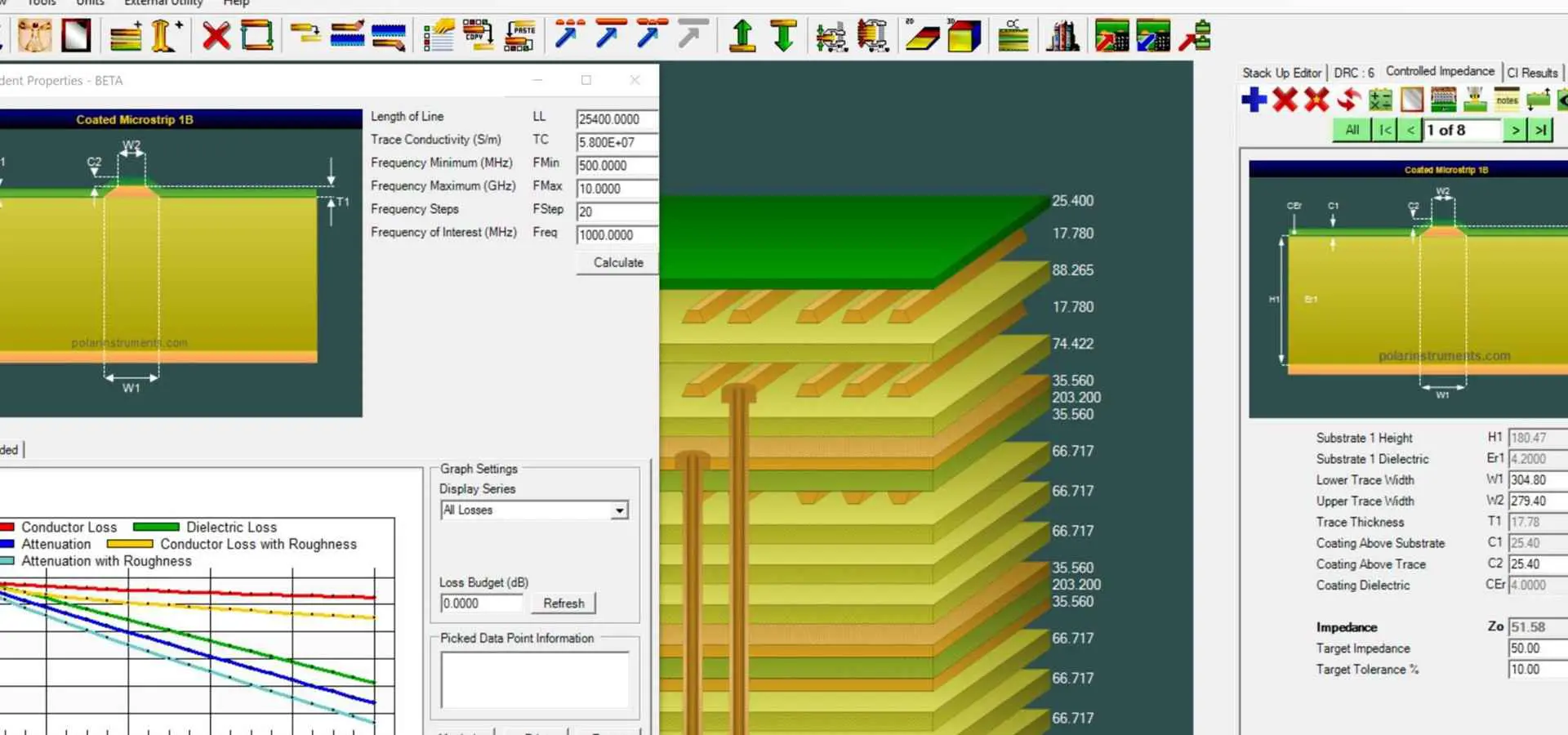
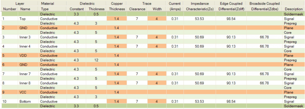
With electronic design services, you should be able to convert the concept of your product into reality, regardless of the complexity. The skill and experience of the company handling your PCB design should be displayed from the initial discussion down to the validation of the final product.

Furthermore, all the products must be well-engineered, usually attractive, built, and at times possess all three features. Also, any state-of-the-art ems company develops the custom housings routinely in line with the form factors of the printed circuit board (PCB) and they should give you some advice regarding the right material, whether injection-molded plastic, aluminum, or stainless steel.

The electronics engineering services include

  • Digital and analog contract printed circuit board (PCB) design
  • Contract PCB layout and schematic capture
  • Power switching drive and circuits
  • 3D modeling and enclosure design
  • Intrinsically safe systems, barriers, and power
  • RF site assessment and design
  • DFM and DFX analysis
  • Simulation, prototypes, and breadboarding
  • Validation, which includes assessment of the CE precertification, environmental compliance, emissions compliance & electromagnetic immunity, design effects analysis and failure modes, Life testing, and custom test procedures and fixtures.

Note than OEMs have to expect support with the development of the product meeting the AS 9100, ISO 13485, and ISO 9001 standards.

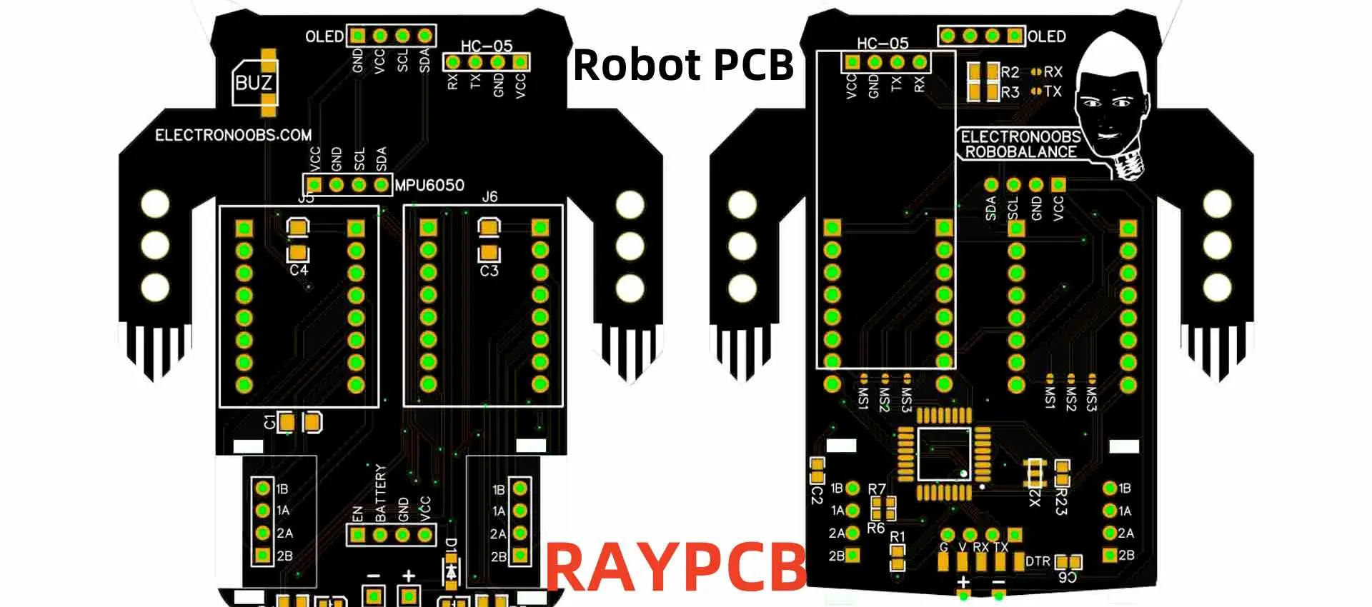
PCB Assembly Services Using Surface Mount Technology

PCB assembly or printed circuit board assembly involves the use of the surface mount technology, as well as through hole technology in soldering components such as integrated circuits, resistors, transistors, onto a specific bare board. With a completed PCB, you will be able to route the signals and power between the physical devices.

Furthermore, through hole technology takes a bit longer because it has to do with more of human interactions with the circuit board. So also, the surface mount technology is better advanced, and is known as the standard for majority of modern products.

In addition, the advanced and professional electronics manufacturers have the ability to transform the aged through hole products in more SMT-designed modern products in order to maximize the usability and lifespan of their life. We can give merit to the improved state-of-the-art machinery, which has improved in both accuracy and speed.

The parts of the circuit board are very small. Therefore, you may not know that you are not building it the right way until you decide to test it. Gladly, the full electronics manufacturer will provide complete in-house functional testing services.

Cable Assembly

cable assembly

Custom mechanical and cable assembly can be a great experience when you are working with the top electronics manufacturers. Dealing in very harsh environment cables, companies involved in electronics contract manufacturing must have the ability to engineer, conduct test, and also produce high-quality cable assemblies. These include harnesses, micro connectors, as well as complex subassemblies.

Cable assembly has more than just these services. The other products linked with the following services are: harnesses, cable assemblies in a harsh environment, control boxes/panels, panel assembly and wiring, and mechanical subassemblies.

Also, this well-rounded electronics manufacturing services will help in engineering, testing, and manufacturing process of the products.

Concerning cable assemblies, hand soldering is used for the manufacturing. Ensure that your vendor has the certification for this. Also, many companies offering electronic manufacturing services may possess a capability known as injection over-molding. This is a process whereby you create a single part making use of multiple materials. The initial material, which is referred to as the substrate at time, is partially covered at least by the subsequent materials during manufacturing.

Ask yourself if your vendor offers over-molding capabilities. Before buying, it is advisable to check it out. Testing time? The cables can get a pull test and functional test. This process of testing does not require much rigorousness like the PCB assemblies.

Electromechanical Assembly

Here, these electronic manufacturing services deal with products like box builds. With respect to the manufacturer, the enclosure can come in plastic, aluminum, and steel. The top electronics manufacturers can have a dedicated team for the final assembly for delivering these services.

Vendors can also provide functional testing, shipment packaging, encapsulation, configuration management, potting & use of heat shrink and 3-D modeling.

Configuration management has to do with establishing consistency in the look and performance of the product. Potting deals with filling the completed assembly using good stuff in improving shock, vibration, moisture, corrosion, and shock resistance. Furthermore, heat shrink can be referred to as plastic tubing that is shrinkable, which goes over its cable.

When conducting any electromechanical assembly, you must practice intrinsic safety at all times both in the process of electronics manufacturing and during the design stage.

Contract Design

At times, you will require an expert, and this expert may not reside in your building, which is fine. When you contract your design, it will allow you to take advantage of the electronics industry specific production teams and expert engineers. They help generate validation tests, firmware and software, DFX analysis (which includes cost-effectiveness, testability, and design for manufacturability), and environmental compliance tests.

Furthermore, the vendor should engage in this while offering documentation of all the steps throughout the electronics contract manufacturing process. In addition, the company engaging in electronic manufacturing services must meet regulatory approval.

However, Electronics manufacturing services (EMS) can shine effectively when the vendor is actively involved in the development process of the product. This means that the vendor is actively involved even before starting the product design.

Furthermore, electronic manufacturing services has to include the material manager, engineers, as well as others that assist in refining the contracted design all through the process of testing, costing exercises, circuit prototyping and simulation, studies in technical feasibility, quality review, costing exercises, physical modeling and 3-D CAD.

Testing

Before your circuit board arrives at your doorstep, you have to ensure you are getting exactly what you have paid for. This refers to a fully functional and properly assembled board. If you get anything less, this can compromise the supply chain. Failure to commit to the PCB testing could

  • Hamper the lead times
  • Harm your company and productโ€™s reputation
  • Cost additional money to help fix issues

There are staggering ways by which your electronic contract manufacturing services can test the PCB assembly. The offering of manufacturers can range from the basic or visual inspection, down to the functional test (this allows for turnkey operation).

PCB testing types includes the following, but arenโ€™t limited to them:

  • AOI (automated optical inspection)
  • Burn-in testing,
  • In-circuit testing,
  • Flying probe testing,
  • Other forms of functional testing

Note that, if you choose extensive testing before receiving your product, then you will discover that it was constructed in line with your specifications. Importantly, you will know if there is a need for your product to undergo additional testing or is set to deliver to your customers.

Prototyping

Note that messing up the rollout of the electronic device could be expensive and painful. With PCB prototyping, you will be able to prevent any embarrassing situation or scenario when heading to launch. Majority of the prototyping justifications are clear and obvious, however, not all.

Durability of the product:

In our world, the product must be able to withstand at least any of these: shock resistivity, power variations, or temperature variations

Design fault checks:

Companies offering expert electronic contract manufacturing services will be able to detect human and technical faults easily. Then it can recommend some improvements before you go ahead with finalizing the design.

Protecting the budget:

It is important to know if the product is meant for the masses, or for a specific niche market. This is because redoing it will be very expensive. Once the last PCB design is heading to mass production, then there is no going back.

Inspecting the product characteristics:

At times, a productโ€™s practical values are a shade off of the theoretical vales, which are considered in the stage of design. With prototypes, you will be able to check as well as update the values.

The prototyping services of printed circuit boards usually take any out of the four forms. Going doing that list, this build now becomes more complete:

  • Proof of concept
  • Visual model
  • Working prototype
  • Functional prototype

Aftermarket Services

The commitment of the company offering electronic manufacturing services to deliver customer satisfaction has to continue for a long time after the delivery of the product. There are three main qualities that you need to check for in providers of electronics aftermarket services. These include technology, expertise, and experience.

Regardless of the place where your consumer or industrial was made or the motive behind the manufacturing, the provider of the electronics manufacturing services has to possess the necessary know-how in servicing it properly. The services here include:

  • Calibration
  • Remanufacturing
  • Refurbishing
  • Burn-in
  • Automated system simulation
  • Electromechanical and Electrical
  • Component-level troubleshooting

Also, the products serviced include:

  • Industrial cabling
  • Single-board computers
  • Distributed control systems
  • HMI and Displays devices
  • Consumer electronics
  • Base stations and RF handhelds
  • Underground mining electronics

Other Capabilities include:

  • Sandblasting
  • Low temperature drying oven
  • Cleaning
  • Thermal testing
  • High pressure spray washer
  • Conformal coating
  • Bringing the units to the OEM specifications
  • Repair analysis via customer, product group, or part number
  • Painting facility
  • Two eye inspections
  • Cable-cleaning machine (can clean any length within seconds)
  • Drying oven with low temperature

This may include the work on the manufactured products by a different company and on the legacy products, which requires sustaining engineering. There are some providers of electronic manufacturing services that can assist you in getting ahead of the problems with failure analysis. Furthermore, if you repeat this same repair, then the provider can come in to quote a redesign, which will save you some money in the future.

Obsolescence Management

A very similar problem in electronics manufacturing is Obsolescence. This is a point whereby a part is coming close to its end, and then the supplier will definitely be able to give you a quote for new supplies, so that you wonโ€™t be taken unawares.

The provider of electronic manufacturing services will give you three recommendations. These include

Last time buy: This is the final purchase in bulk before the part is discontinued by the maker.

End of life: The part isnโ€™t useful anymore and isnโ€™t support any longer

No recommendation for the new design: The partโ€™s future is not certain, is outdated, and carries the risk of becoming obsolete.

To assist with the managing of component obsolescence, the vendor should be able to provide life-cycle analysis. The assessment checks the componentโ€™s entire environmental impacts via its whole life. Even before the production is completed, the vendor will proactively search for parts that need replacement and then assist you in obtaining alternatives.

Therefore, even with the word โ€˜aftermarketโ€™, there are some services which will benefit you even before the customers see the end result. Before you go ahead to send your product to the market, there is a need to understand and know the risks involved.

Your Choice of Vendor Matters

You can see that this is just the beginning of the electronic manufacturing services. It is clear that the delivery you get is determined and varies by vendor. Also, there are some just seeking to print the bare boards in large volumes. For others, they offer creative and complex solutions in much smaller volumes. They also assist you with different steps in the supply chain.

Are you taken aback to see how much the best provider of electronic manufacturing services have to offer? You donโ€™t need to be in any way. In addition, there are three major reasons why the best consumer electronics manufacturer provides all in one services:

  • More investment in the projectโ€™s success
  • Understanding your goals and project completely and less miscommunications
  • Fewer transportation and shipping costs, as well as delays

Conclusion

Electronic manufacturing services are always evolving and has a fast pace. The flexible solution providers that are useful in offering electronic components. Also, this helps in keeping pace with this quick change and will keep experiencing and delivering success to themselves and to their customers.

We at Rayming PCB have developed a global business, which is established on the backing of complex high mix low volume devices. Also, we help in solving the different challenges related to global electronics.

Robot PCB Assembly: Design and Manufacturing for Robotics Applications

The integration of printed circuit boards (PCBs) in robotics has revolutionized the way autonomous systems operate, communicate, and interact with their environments. Robot PCB assembly represents a specialized field within electronics manufacturing that combines the precision demands of robotics with the complexity of modern circuit board design. As robotics applications continue to expand across industries from manufacturing and healthcare to consumer electronics and space exploration, the need for sophisticated, reliable, and efficient robot PCB solutions has never been greater.

YouTube video

Understanding Robot PCB Fundamentals

Robot PCBs differ significantly from conventional circuit boards due to the unique operational requirements of robotic systems. These boards must withstand constant motion, vibration, temperature fluctuations, and electromagnetic interference while maintaining precise control over motors, sensors, and communication systems. The design philosophy behind robot PCB assembly prioritizes durability, signal integrity, and real-time processing capabilities that enable seamless human-robot interaction and autonomous decision-making.

Modern robotics applications demand PCBs that can handle multiple simultaneous functions including sensor data processing, motor control, wireless communication, and power management. This multifaceted approach requires careful consideration of component placement, thermal management, and electrical isolation to prevent interference between different subsystems. The complexity of these requirements has led to the development of specialized design methodologies and manufacturing processes tailored specifically for robotic applications.

Design Considerations for Robotic PCB Systems

The design phase of robot PCB assembly begins with a thorough analysis of the robotic system’s operational requirements. Engineers must consider factors such as power consumption, processing speed, environmental conditions, and mechanical constraints when developing the circuit board architecture. One critical aspect is the selection of microcontrollers and processors that can handle real-time control algorithms while maintaining low power consumption for battery-operated robots.

Signal routing in robot PCBs requires particular attention to minimize electromagnetic interference (EMI) and crosstalk between high-speed digital signals and sensitive analog sensor inputs. The use of ground planes, proper trace routing techniques, and strategic component placement helps maintain signal integrity across the board. Additionally, the integration of power management circuits must be carefully planned to provide stable voltage levels to various subsystems while implementing efficient switching regulators to maximize battery life.

Thermal management becomes increasingly important in compact robotic designs where heat dissipation is limited. The placement of high-power components such as motor drivers and processors must be optimized to prevent thermal coupling and ensure reliable operation across the robot’s operational temperature range. This often involves the use of thermal vias, heat sinks, and copper pour techniques to distribute heat effectively across the PCB.

Component Selection and Integration

The selection of components for robot PCB assembly requires balancing performance, size, cost, and reliability considerations. Microcontrollers specifically designed for robotics applications often feature integrated motor control peripherals, analog-to-digital converters for sensor interfacing, and communication interfaces such as UART, SPI, and I2C. Popular choices include ARM Cortex-M series processors, which offer excellent real-time performance and low power consumption.

Sensor integration represents another crucial aspect of robot PCB design. Modern robots typically incorporate multiple sensor types including accelerometers, gyroscopes, magnetometers, proximity sensors, and cameras. The PCB must provide appropriate analog conditioning circuits, voltage level translation, and noise filtering to ensure accurate sensor readings. Inertial measurement units (IMUs) require careful placement away from magnetic interference sources and proper decoupling to maintain measurement accuracy.

Motor control circuits form the backbone of most robotic systems, requiring robust driver circuits capable of handling the current and voltage requirements of various actuator types. The selection between brushed and brushless motor controllers depends on the specific application requirements, with brushless controllers offering higher efficiency and longer lifespan at the cost of increased complexity and cost.

Manufacturing Processes and Quality Control

Robotics Integration

The manufacturing of robot PCBs follows specialized processes designed to meet the stringent reliability requirements of robotic applications. Surface mount technology (SMT) assembly has become the standard for most robot PCB manufacturing due to its ability to achieve high component density and excellent mechanical stability. The SMT process involves solder paste application through precision stencils, component placement using high-accuracy pick-and-place machines, and reflow soldering in controlled temperature profiles.

Quality control measures in robot PCB manufacturing include automated optical inspection (AOI) to detect component placement errors, in-circuit testing (ICT) to verify electrical connectivity, and functional testing to ensure proper system operation. These testing procedures are particularly important for robotic applications where field failures can result in costly downtime or safety hazards.

The use of lead-free soldering processes has become standard in robot PCB manufacturing to comply with environmental regulations and ensure long-term reliability. However, the higher processing temperatures required for lead-free soldering can present challenges for temperature-sensitive components, requiring careful process optimization and component selection.

Advanced Technologies in Robot PCB Design

The evolution of robotics has driven the adoption of advanced PCB technologies including flexible and rigid-flexible designs that can accommodate the mechanical constraints of articulated robotic systems. Flexible PCB enable connections between moving parts while maintaining electrical continuity, making them ideal for robotic joints and rotating assemblies.

High-density interconnect (HDI) technology has become increasingly important for compact robotic designs where space is at a premium. HDI techniques such as microvias, embedded components, and sequential build-up processes allow for increased routing density while maintaining signal integrity. This technology is particularly beneficial for mobile robots and drone applications where weight and size constraints are critical.

The integration of wireless communication capabilities into robot PCBs has opened new possibilities for remote control, data logging, and swarm robotics applications. The design of antenna circuits and RF shielding requires specialized knowledge to prevent interference with other electronic systems and ensure reliable communication performance.

Power Management and Energy Efficiency

Power management represents one of the most critical aspects of robot PCB design, particularly for autonomous mobile robots that rely on battery power. Efficient power management circuits must provide stable voltage rails to various subsystems while minimizing power consumption to extend operational time. The use of switching regulators, low-dropout regulators, and power management ICs specifically designed for robotics applications helps optimize energy efficiency.

Battery management systems integrated into robot PCBs monitor cell voltage, current, and temperature to prevent overcharging, over-discharging, and thermal runaway conditions. These systems are essential for ensuring safe operation and maximizing battery lifespan in robotic applications. The implementation of sleep modes and power gating techniques allows robots to reduce power consumption during idle periods while maintaining the ability to respond quickly to external stimuli.

Energy harvesting technologies are increasingly being integrated into robot PCB designs to supplement battery power in specific applications. Solar cells, piezoelectric generators, and thermoelectric devices can provide additional power sources for sensors and low-power circuits, extending the operational range of autonomous robots.

Connectivity and Communication Systems

Modern robot PCBs must support multiple communication protocols to enable interaction with other systems, sensors, and network infrastructure. The integration of wired and wireless communication interfaces requires careful consideration of signal integrity, power consumption, and electromagnetic compatibility. Common communication standards include Ethernet, USB, CAN bus, and various wireless protocols such as Wi-Fi, Bluetooth, and Zigbee.

The design of communication circuits must account for the harsh electromagnetic environment typically encountered in industrial robotic applications. Proper shielding, filtering, and isolation techniques help prevent interference from motor drives and switching power supplies that can disrupt sensitive communication signals.

Real-time communication capabilities are essential for many robotic applications, particularly those involving coordinated motion or safety-critical operations. The implementation of time-sensitive networking protocols and deterministic communication stacks requires specialized hardware and software design considerations.

Testing and Validation Methodologies

The testing and validation of robot PCBs involves comprehensive procedures that verify both electrical functionality and mechanical reliability. Environmental testing includes temperature cycling, vibration testing, and humidity exposure to simulate real-world operating conditions. These tests are particularly important for robots operating in harsh environments such as manufacturing facilities, outdoor applications, or space missions.

Functional testing of robot PCBs requires specialized test fixtures and software that can simulate the full range of robotic operations. This includes testing motor control algorithms, sensor calibration procedures, and communication protocols under various operating conditions. The use of hardware-in-the-loop (HIL) testing systems allows for comprehensive validation of control algorithms before deployment.

Electromagnetic compatibility (EMC) testing ensures that robot PCBs meet regulatory requirements and do not interfere with other electronic systems. This testing is particularly important for robots operating in sensitive environments such as hospitals, laboratories, or near critical infrastructure.

Future Trends and Innovations

Line following robot

The future of robot PCB assembly is being shaped by several emerging technologies and trends. The increasing adoption of artificial intelligence and machine learning in robotics is driving demand for more powerful processing capabilities and specialized AI accelerator chips. These developments require PCB designs that can accommodate high-speed interfaces and provide sufficient power delivery for computational intensive operations.

The miniaturization of robotic systems continues to push the boundaries of PCB design, with the development of three-dimensional circuit architectures and embedded component technologies. These advances enable the creation of smaller, more capable robots while maintaining the functionality and reliability required for practical applications.

The integration of advanced materials such as graphene, carbon nanotubes, and metamaterials into PCB designs offers new possibilities for improving thermal management, reducing weight, and enhancing electromagnetic performance. These materials are particularly promising for aerospace and military robotics applications where performance requirements are most demanding.

Conclusion

Robot PCB assembly represents a rapidly evolving field that combines the precision requirements of robotics with the complexity of modern electronics manufacturing. The successful design and manufacturing of robot PCBs requires a deep understanding of robotic system requirements, advanced PCB technologies, and specialized manufacturing processes. As robotics applications continue to expand across industries, the demand for sophisticated, reliable, and efficient robot PCB solutions will continue to grow, driving innovation in design methodologies, manufacturing processes, and testing procedures. The future of robotics depends heavily on the continued advancement of PCB technologies that can support the increasingly complex requirements of autonomous systems while maintaining the reliability and performance standards essential for practical deployment.

A Comprehensive Guide on Advanced Circuits Stackup

multilayer pcb stackup

The rapid development in the electronics industry has continued to increase the need for lightweight and compact boards. Also, the miniaturization of circuit boards has helped the production of compact and complex electronic devices. Therefore, this development has resulted in the popularity of multilayer boards. These boards involve the combination of two or more double-sided or single-sided boards stacked together.

Proper stackup is crucial in multilayer circuit boards. This is because stackup affects the performance and functionality of a printed circuit board. A multilayer circuit features three or more conductive layers with one layer placed on the insulation board and two layers outside. The increase in the densities and complexities of PCBs could result in issues like stray capacitance, cross-talk, and noise.

What is a Stackup?

A stackup refers to how copper and insulating layers are arranged to create a PCB before board layout design. Also, a stackup enables manufacturers to get more circuitry through different PCB board layers.  A PCB stackup can help to reduce the vulnerability of a circuit to external noise. Also, it reduces radiation and crosstalk concerns on high-speed PCB layouts.

A multilayer circuit board comprises inner signal layers, power plane, and ground plane. Several layers in a circuit board help to increase the ability of a board to disperse energy. ย A PCB stackup is simply the arrangement of copper and insulating layers in a circuit board design. Manufacturers arrange these layers to achieve functionality in circuit boards.

Optimal stackup in multilayer circuits is one of the most crucial factors that determine electromagnetic compatibility (EMC) performance. A good layer stack-up can reduce radiation and can prevent interference in circuits caused by external noise sources. Also, a well-stacked circuit board substrate can minimize impedance mismatch and crosstalk issues. However, a poor stackup can result in EMI radiation since ringing and reflections in the systems can reduce PCB performance.

Common Types of PCB Layer Stackups

10 Layer PCB Stackup

There are various PCB board layers. The EMC requirements of the board and the size of the circuit are factors that determine the number of layers in a board. After determining the number of layers your board needs, you will have to determine the board layout.

2 layer stackup

A 2 layer board which is also known as a double-sided board is a type of multilayer board that allows interconnects on both sides. These circuit boards comprise three material layers which are the signal layer, laminate core, and bottom layer.  Two of these layers are functional.

Also, the signal layer is the top layer. It features copper within a particular range of thickness. The laminate core is the layer that separates the bottom and top copper layers. Therefore, it keeps the copper layers isolated. The bottom layer is similar to the signal layer. It is the second layer of copper.

4 layer stackup

 A 4 layer PCB stackup features 4 layers to route electrical signals. Also, the PCB manufacturer sandwiches these layers together.  These layers are the bottom layer, top layer, and two inner layers. The bottom and top layers are on the outside while the two inner layers are between them. Manufacturers place components on the top and bottom layers of a 4 layer PCB.

The inner layers canโ€™t create external connections. Therefore, they serve as power planes for routing signals. This helps to improve trace signal quality and also minimize EMI emissions. It is not advisable to make the inner layers signal layers. If your PCB project requires four signal layers, you will need to consider the 6 layer PCB stack up.

The 4 layer PCB stack up comprises top layer-inner layer 1- inner layer 2-bottom layer. Also, the 4-layer PCB stackup offers enhanced functionality. However, the 4 layer PCB stack up may not be ideal for some applications. You can switch the ground layers of a 4 layer PCB stack up based on the layer having more signals. A 4 layer PCB stackup features the power and ground planes as the inner layer. A 4 layer stackup produces a board thickness of 0.062.โ€

6 layer stackup

A 6 layer stackup is a 4 layer stackup with two more signal layers. Therefore, 6 layer stack up comprise four routing layers and two internal planes for power and grounding. This means that a 6 layer stack up comprises two outer and two internal layers, one ground plane, and one power plane.

This stackup arrangement for a 6-layer PCB is very common. This is because this stackup arrangement provides a balance between high-speed signaling and EMI control. Also, this stackup runs high-speed signals via the two buried layers. However, this design isnโ€™t ideal for all applications.

For instance, you will need to place the power planes and ground planes close to each other for high-speed designs.  A 6 layer stackup feature board thickness between the range of 0.031 and 0.062

8-layer stackup

An 8 layer PCB stackup provides better options as it adds two more layers for performance or routing. Also, it is an advanced circuit stack up that sets to achieve the objectives of a multilayer PCB design. A typical 8 layer stackup comprises ground and power planes in the center. Therefore, this provides great capacitance between layers. Also, it protects signal integrity by separating the second and third signal planes.

An 8 layer stack up comprises four signal layers, two power planes, and two ground planes. Also, 8-layer stackup doesnโ€™t include more than four signal layers. Rather than adding more signal layers, this PCB includes more ground and power planes. The board thickness for an 8 layer board is available in 0.093โ€, 0.0125โ€, and 0.062.โ€

10 layer stackup

If the requirement of your PCB design involves six routing layers, a 10 layer stack up is an ideal choice. A 10 layer PCB stackup comprises four planes and six signal layers. Therefore, it features a tight coupling between the return and signal planes. A 10 layer stackup offers board thickness that ranges from 0.062โ€ and 0.125.โ€

This PCB stackup arrangement routes high-speed signals on the internal signal layers. Therefore, this stackup offers exceptional signal integrity when properly routed and stacked. Also, it offers excellent EMC performance. It isnโ€™t advisable to replace any of the power or ground planes with signal layers. If you do so, it could lead to poor performance. A 10 layer PCB stackup features multiple ground planes.

Objectives of a Multilayer PCB Stackup

FULL PCB MANUFACTURING Quote

While creating a multilayer stack up, manufacturers set out to achieve some objectives. Multilayer stackups design must meet certain design requirements. Therefore, multilayer boards should achieve the following objectives:

  • Signal layers must be adjacent to planes
  • Multiple ground planes lower impedance and radiation
  • Ground and power planes must be closely coupled together
  • Route high speed signals through buried layers between planes
  • Signal layers must be closely coupled to their planes

While achieving these objectives is crucial, it is crucial to know that not every PCB layer stack up will meet all these objectives. Therefore, it is important to work with professional engineers to determine the objectives you should prioritize.

Benefits of PCB Layer Stackups

A PCB stackup offers a lot of benefits in electronics devices. The introduction of multilayer boards has contributed to the development of advanced electronic devices. Also, multilayer boards comprise at least three conductive layers. Due to the number of conductive layers in these boards, they offer great functionality. While PCB layering may be more complex, PCB stackups offer these benefits:

Reduce vulnerability

Multilayer PCBs can shield an inner layer from external noise. Therefore, this makes them less vulnerable to exterior forces. Also, it can reduce radiation and impedance problems on high-speed systems.

Improve functionality

Multilayer PCBs can improve the functionality and speed of an electronic device. Also, these boards can enhance electromagnetic compatibility of a board. Also, solid ground planes and power planes can help to minimize EMI emissions. This can as well improve signal quality on the traces.

Minimize costs

A properly arranged PCB stack up can help to achieve lower production costs. This is because these stackups place multiple circuits on a single board.

Reduce radiation

A good stackup can reduce radiation from an electronic device, particularly in high-speed boards. Therefore, it is crucial to arrange PCB stackup with functionality in mind. This is because poorly stacked layers can cause impedance mismatches and this can lead to greater EMI radiation.

Factors to Consider when Creating a Multilayer Stackup

There are design factors you need to take into consideration when designing a multilayer stackup.

Core materials

For a normal single sided board, a manufacturer can use aluminum cores. Aluminum cores are not ideal for multilayer stackups. This is because multilayer aluminum boards are very difficult to fabricate.

Interlayer offset

PCB layers can be offset when fabricating a multilayer PCBs. Therefore, you can prevent this by using rivet and bowel method and hot melting for PCB design.

Bow and twist

Bow and twist can result from uneven distribution of copper in a multilayer stackup. Therefore, ensure you design all multilayer boards symmetrically.

The inner layer copper thickness is a crucial factor when arranging PCB stackups. This is because board thickness offers great functionality. With the right PCB layer stack, you can achieve great functionality. Also, the board thickness is crucial when creating a multilayer stackup.

Conclusion

To maintain signal performance in a PCB layer stackup, the power plane is usually close to the ground plane. Multilayer printed circuit boards offer great benefits. Therefore,  a good layer stackup is critical in ensuring functionality in these boards. Multilayer PCBs can have a board thickness that ranges from 0.4mm to 3.2mm.

Xilinx XC2C32A-6QFG32Iโ€™s Technical Specifications, Buying Guide & Comparison with FPGA

Xilinx XC7Z010-2CLG400i

Ordinarily, a Complex Programmable Logic Device (CPLD) may pass for a Programmable Logic Array (PLA) because of the connection format.

However, a CPLD, as the name signifies, is more complex than a traditional PLA. If you are looking to invest in one, consider the Xilinx XC2C32A-6QFG32I. Manufactured by Xilinx, it is optimized for low-power and high-performance applications.

In this article, we discuss the technical specifications of the chip. We also cover the buying guide/the things to look for before buying the Xilinx XC2C32A-6QFG32I. Finally, we compared the Xilinx XC2C32A-6QFG32I to a Field Programmable Gate Array (FPGA).

Technical Specifications of Xilinx XC2C32A-6QFG32I

The table below represents the different values of the components making the Xilinx XC2C32A-6QFG32I CPLD.

Technical AttributesDescription
Type of ProgrammingIn System Programmable
Package/Case32-VFQFN (Exposed Pad)
Propagation Delay Time6 nanoseconds (ns)
Operating TemperatureBetween 40 and 85-degree Celsius
Operating Voltage Supply (minimum to maximum)1.7V to 1.9V
Mounting StyleSurface Mount Technology (SMT)
Number of Logic Elements (LE)2
Speed Grade6
Number of Macrocells32
Number of Logic Gates750
Number of I/Os21
Screening LevelIndustrial
Maximum Internal Frequency300 MHz
Moisture Sensitivity Level (MSL)3 (168 hours)


Xilinx XC2C32A-6QFG32I Buying Guide

No doubt that the Xilinx XC2C32A-6QFG32I is one of the high-performance and low-power Complex Programmable Logic Devices (CPLDs).

However, to be on the safer side, consider checking out some things before you place your order. Here is a list of some of the things you want to check before ordering for the Xilinx XC2C32A-6QFG32I CPLD:

1. Capability of the I/O

The Input and Output (I/O) is one of the most important factors to consider. It deals on the number of pins used in configuring the chip.

For emphasis, you want to concentrate on specific aspects of the I/Oโ€™s capabilities. Here are some of the areas of concentration.

The type of logic is worth considering. This is so because its capability should be able to increase the overall functionality of the chipโ€™s design.

The next thing to look into (as per the I/O) is the independence of the I/O. We must mention that not all I/Os are independent. Some need to be tied to the master reset and clock input as dedicated I/Os to help their operations.

The output capability of the I/Os is another important factor to consider. It has to do with the current and voltage levels supported by the I/O.

2. Programming Technology

What type of programming technology is required to configure the Xilinx XC2C32A-6QFG32I CPLD?

The programming technology helps determine the number of configurations due for the chip.

The most popular programming technologies are:

3. The Function Blockโ€™s Capability

What can the Function Block do towards the improvement of the Xilinx XC2C32A-6QFG32I design?

The things to look into here include the minimum and maximum propagation delay timeframes (in nanoseconds) for the Function Block.

You also want to check the number of Function Blocks in the Xilinx XC2C32A-6QFG32I CPLD and whether these Function Blocks have any need for additional logic resources.

Xilinx XC2C32A-6QFG32I vs FPGA

Xilinx XC2C32A-6QFG32I CPLD has some advantages over a Field Programmable Gate Array (FPGA).

Here are some of them:

  • Xilinx XC2C32A-6QFG32I CPLDโ€™s memory architecture is persistent, meaning that it doesnโ€™t wipe out the memory even if the device shuts down. This is unlike most FPGAs that use the SDRAM memory that clears data once the circuit is off.
  • Xilinx XC2C32A-6QFG32I propagation delay is more predictable than that of an FPGA. Most FPGAs propagation delays are unpredictable because of the reconfigurable design of the circuit.
  • Last but not least, Xilinx XC2C32A-6QFG32Iโ€™s CPLD is a competitive option to an FPGA because it has a lower development cycle. Therefore, it will hit the market faster than an FPGA would.

Conclusion

Need professional advice on how to get started with the Xilinx XC2C32A-6QFG32I? Do not hesitate to contact RayPCB.

What You Need to Know before Buying the Xilinx XC2C64A-7QFG48I

xilinx spartan 3

The best way to buy or invest in a Field Programmable Gate Array (FPGA) is to be certain of what it has to offer. Today, we have more FPGA consumers that are either unsure of the capability of the board or simply donโ€™t know the components that make it up.

We hope to simplify the process for you so you can make an informed decision. In this article, you will learn more about some of the important features and technicalities worth knowing before buying the Xilinx XC2C64A-7QFG48I.

What is the Xilinx XC2C64A-7QFG48I?

Xilinx XC2C64A-7QFG48I is a part of the CoolRunner-II series. For emphasis, the series include Field Programmable Gate Arrays (FPGAs) and Complex Programmable Logic Devices (CLPDs) designed to help bolster the performance of the circuit board.

As a consumer, it is expedient that you understand how these components can come together to make a unified circuit board peripheral.

According to Xilinx, the manufacturer of the Xilinx XC2C64A-7QFG48I, the FPGA cum CLPD can be used in both high and low applications. In that case, it can be used for low-powered applications, while helping in the improvement of higher performances in the applications.

Technical Specifications of Xilinx XC2C64A-7QFG48I

FULL PCB MANUFACTURING Quote

In this section, we give a breakdown of the specifications, parameters and components that make up the technical attributes of the Xilinx XC2C64A-7QFG48I.

Logic Components

The logic components making up the Xilinx XC2C64A-7QFG48I are the Logic Elements (LE) and Logic Array Blocks (LABs). As CLPDs and FPGAs cannot make do without these, the provision thereof help in bolstering the performance of the IC.

First, the Logic Elements (LE) or cells are made up of 4 blocks. Second, the Logic Array Blocks (LABs) are made up of the same composition โ€“ 4.

On the other hand, the Xilinx XC2C64A-7QFG48I is made up of 1,500 logic gates. These logic components come together to combine functions that make Xilinx XC2C64A-7QFG48I one of the best CLPDs you can work with out there.

Operating Temperature

Xilinx XC2C64A-7QFG48Iโ€™s operating temperature is a little bit above the industry standards. The rating is 40-degree Celsius minimum and 85-degree Celsius maximum.

The regulation of temperature and heat dissipation is an important element worth considering in the FPGA design process.

In addition to the operating temperature, Xilinx XC2C64A-7QFG48I also has a rated Moisture Sensitivity Level (MSL) of 3, equivalent to 168 hours 7 days. What this means is that after 7 days of exposure to ambient room conditions, the Xilinx XC2C64A-7QFG48I may be susceptible to certain damages.

Mounting Technology

The Surface Mount Technology (SMT) has become a standard of sorts for placing components atop an electronic device.

The same is the case with the Xilinx XC2C64A-7QFG48I. It uses the Surface Mount Technology (SMT) to place components on the CLPD using Surface Mount Devices (SMDs).

Voltage Supply

Last but not least is the voltage supply. It has to do with the supply of current (voltage) throughout the CLPD and at which rate?

Xilinx XC2C64A-7QFG48Iโ€™s internal voltage supply is between 1.7 volts and 1.9 volts. The rated operating voltage supply is 1.8 volts.

Conclusion

You can be confident of getting value for money when working with the Xilinx XC2C64A-7QFG48I. Contact RayPCB with your specifications and to get a quotation.

What You Need to Know About Xilinx XCZU9EG-2FFVB1156I SoC FPGA

Xilinx XC7Z020-2CLG400i

Xilinx XCZU9EG-2FFVB1156I doubles as a System on a Chip (SoC) and a Field Programmable Gate Array (FPGA).

It is one of the SoCs categorized under the Zynq UltraScale + MPSoC series by Xilinx. In this article, you will learn about some of the things you needed to know about this Integrated Circuit (IC).

Powered by Powerful Processors

In line with latest trends in FPGA development, the Xilinx XCZU9EG-2FFVB1156I is powered by some of the best processors.

These processors are sourced from ARM, one of the leading brands in the market. As per the information in the datasheet, Xilinx XCZU9EG-2FFVB1156I is powered by three (3) core processors.

Here are some of the processors and what they have to offer:

1. ARM Mali-400 MP2

ARM Mali-400 MP2 is one of the processors used in Xilinx XCZU9EG-2FFVB1156Iโ€™s design. According to NotebookCheck.com, the processor is an OpenGL ES 2.0-capable GPU used for System on a Chip (SoC) manufactured by ARM.

The ARM Mali-400 MP2 is the GPUโ€™s version of two cores and a vertex processor.

One of the attributes is cost-saving, being that the manufacturer designed it to reduce both the bandwidth and power consumption of devices.

2. ARM Cortex R5

The ARM Cortex R5 is another core processor used in Xilinx XCZU9EG-2FFVB1156I. It helps on enabling the implementation and integration of the Xilinx XCZU9EG-2FFVB1156I SoC into both safety-critical and embedded real-time applications.

3. ARM Cortex A53

This is the third core processor found in Xilinx XCZU9EG-2FFVB1156I. Its primary function is to provide improved performance for a wide range of applications, such as aerospace, storage, mobile and automobile applications.

Technical Specifications of Xilinx XCZU9EG-2FFVB1156I

Now that you know some of the core processors, let us talk about the technical attributes. The table below shows some of the technical elements or components making up the Xilinx XCZU9EG-2FFVB1156I System on a Chip (SoC).

Technical AttributesDescription
Number of Logic Elements (LE)599,500
Number of Logic Array Blocks (LABs)34,260
Distributed RAM8.8 Mbit
Embedded Block RAM (EBR)32.1 Mbit
Operating Temperature (min-max)40-degree Celsius to 100-degree Celsius
Number of Cores7
Moisture Sensitivity Level (MSL)Yes, 4 (72 hours)
RAM Size256 kilobytes
Package/Case1156-BBGA, FCBGA
Number of Transceivers24
Number of I/O352
Clock Frequency (maximum)600 MHz, 667 MHz, and 1.5 GHz

Xilinx XCZU9EG-2FFVB1156I Buying Guide

Certain factors are worth considering before paying for a Field Programmable Gate Array (FPGA) or a System on a Chip (SoC).

In the case of Xilinx XCZU9EG-2FFVB1156I, here are some of the things we would like you to look out for.

1. Connectivity and Peripherals

One of the things you want to look for is both the connectivity and peripherals making up the IC. For example, the peripherals and connectivity help bolster the transmission of data and signals on the board.

Xilinx XCZU9EG-2FFVB1156I has several connectivity options, ranging from CANbus, USB OTG and Ethernet.

2. Buying Source

Where do you intend on buying the Xilinx XCZU9EG-2FFVB1156I SoC? The supplier should among many other things, have a Minimum Order Quantity (MOQ), competitive pricing and faster delivery timeframe.

Conclusion

To wrap it up, contact RayPCB to help configure the Xilinx XCZU9EG-2FFVB1156I SoC with all the additional components and specifications you want it to have.

How the Xilinx Board is improving the Future intelligent of Electronics

Xilinx Virtex-5 fpga

Xilinx SoC and FPGA boards offer you with hardware platforms to enhance your development time. If you need an evaluation board or a development board, Xilinx boards are an ideal option for you. Also, Xilinx solution enables differential systems that integrate the greatest levels of software-based systems with hardware optimization.

Xilinx offers the most comprehensive set of hardware platforms in the industry. This helps to speed your time-to-revenue application. Also, Xilinx boards offer a wide range of capabilities and features which make them widely used across several fields.

What is the Function of a Xilinx Board?

There is a thin line between hardware and software engineering. FPGAs feature physical attributes that can be easily manipulated via the utilization of hardware description languages (HDL). Also, FPGAs bridge the gap between programming hardware and programming software.

The Xilinx board is a semiconductor device based around the configurable logic blocks (CLBs) linked through programmable interconnects. Also, you can reprogram this board to desired application after manufacturing. Therefore, this makes the Xilinx FPGA board different from ASICs.

The Xilinx board offers the greatest product portfolio that allows the next generation of advancement in several industries. Also, the Xilinx board comprises CLBs and other features a user can program and reprogram. The basic functionality of this board is wholly built on adaptive hardware. This adaptive hardware enables modification after production.

The adaptability of Xilinx boards distinguishes them from GPUs and CPUs. However, CPUs can be very flexible. One limitation is that they have fixed underlying hardware. Also, you canโ€™t change the hardware of a CPU once manufacturing has taken place. On the other hand, Xilinx boards can process huge amounts of data in parallel.

The Xilinx board helps designers and programmers to update the computer architecture with more flexibility. Therefore, this results in domain-specific architectures. Also, Xilinx boards are becoming necessary due to the innovationโ€™s speed in areas such as artificial intelligence.

Features of Xilinx Boards

xilinx-kintex-ultrascale-development-board

Xilinx boards come with certain features which contribute to their outstanding performance when used in applications. These benefits include:

  • Thousands of Inputs and Outputs
  • High speed with synchronous circuitry about 50 MHz
  • Lower power consumption
  • Programmable logic device
  • System on Chip
  • Programming at Behavioral level
  • Easily configurable
  • Supports programming by using SystemVerilog, SystemC, VHDL, and more
  • Several DSPs/multiplier blocks

Applications of Xilinx Boards

Xilinx boards are widely used across several industries. Over time, these boards have become an integral part of high-performance devices. Also, Xilinx has been engaging several industries and creating deep understanding. The applications of Xilinx boards are vast. These days, they are commonly used in defense, data center, and artificial intelligence.

Automotive

Xilinx boards are widely used in automotive silicone and IP solutions. IP solutions and automotive silicon offer gateway and in-vehicle infotainment.

Consumer electronics

Xilinx boards offer cost-effective solutions which enable next generation consumer applications like digital flat panel displays and home networking. Also, these boards play a crucial role in the development of todayโ€™s consumer electronics.

Computing and data storage

These boards offer great solutions for Storage Area Network (SAN) and solutions for Network Attached Storage (NAS).

Industrial

Xilinx boards are ideal for Industrial, Scientific and Medical (ISM). This allows greater degrees of flexibility and lower overall NRE costs for several applications like industrial automation and industrial imaging.

Video and image processing

The xilinx boards and design platforms allow greater degrees of faster-time-to-market for several video and imaging applications.

Xilinx Board Programming

FULL PCB MANUFACTURING Quote

Xilinx boards utilize an HDL to manipulate circuits based on your desired capabilities. Also, the programming of this board is absolutely different from a CPU or GPU. Xilinx programming involves the use of an HDL to develop circuits and change the hardware based on what you desire to do. Also, this process is similar to software programming where you write code and transform it into a binary file. However, the result is that the HDL allows physical changes to the hardware instead of strictly optimizing the device to manage the software.

Xilinx boards offer a great level of flexibility since you are manipulating the hardware from the bottom. Also, you can adjust functions like power or memory usage based on the project. When we talk about programming a Xilinx board, it is not the same as developing software. Also, programming involves writing and executing code.

Those days, only hardware engineers could program Xilinx boards. However, this is no longer the case. Software developers can utilize various languages to program a Xilinx board without being well scripted in HDLs. Therefore, this eliminates the need to pivot to a new programming language. Also, this can help software developers concentrate on concepts instead of hardware.

There are various mainstream HDLs that can program FPGA today. Below are some of these HDLs and their main attributes

Verilog

Verilog is the first ever created HDL. Today, it is mainly used for test verification and analysis. C was the core of this language.

Lucid

Lucid was specifically designed for FPGAs. It overcame some of the downsides of more archaic languages like Verilog.

VHDL

The VHDL first appeared in the 1980s and depended on Ada and Pascal.

How to Program Xilinx Board

Xilinx boards have always existed in the world of hardware engineers.  However, software programmers and AI scientists can access new platforms that enable the process to feel like writing software. You will get a solution for FPGA programming with the right tool. Therefore, this meets the current knowledge level of hardware and software.

Programming a Xilinx board comprises writing code and translating the program to a low-language. Also, it involves converting the program into a binary file. After this, you need to feed the program to the FPGA board. Also, you will need to have access to the appropriate platform to streamline the programming process.

Conclusion

With the emerging applications, there is more demand for Xilinx boards. The FPGA industry is growing at a healthy rate. The fast changing fields like machine learning and AI need flexible and adaptable architectures. Also, the Xilinx FPGA boards are ready to optimize these new opportunities.

Technical Specifications and Features for Xilinx XC2C64A-7VQ44I

Xilinx Kintex UltraScale FPGA Board

Xilinx XC2C64A-7VQ44I is one of the Complex Programmable Logic Devices (CLPD) designed and categorized under the CoolRunner-II series. As the name signifies, it can be โ€œcomplex,โ€ but you can be confident when it is handled by a professional digital designer.

According to ElProCus, a CLPD is a more โ€œclassy type of chipโ€ in the sense that it is compact and can combine the functions of most logics. For emphasis, it has less logic than a Field Programmable Gate Array (FPGA), but can offer higher performance than a Simple Programmable Logic Device (SPLD).

In this article, you are going to learn more about the Xilinx XC2C64A-7VQ44I technical specifications. We also provided a list of features to help you pick the best Xilinx XC2C64A-7VQ44I in the market.

Xilinx XC2C64A-7VQ44Iโ€™s Technical Specifications

printed circuit board assembly services
Technical AttributesDescription
Number of Macrocells64
Number of Logic Gates1,500
Number of Logic Elements (LE)/Cells4
Number of I/Os33
Propagation Delay Time6.7 ns
Mounting TypeSurface Mount Technology (SMT)
In System ProgrammabilityYes
Type of MemoryROMless
Number of Pins44
Operating Temperature (min to max)40-degree Celsius to 85-degree Celsius
Maximum Operating Frequency159 MHz
Package/Case44-TQFP
Minimum Operating Voltage Supply1.7 volts
Maximum Operating Voltage Supply1.9 volts
Speed Grade7
Maximum Internal Frequency300 MHz
Operating Supply Voltage1.8 volts
Operating Supply Current17 uA
Moisture Sensitivity Level (MSL)3 (168 hours)
Screening LevelIndustrial

Xilinx XC2C64A-7VQ44I Features

1. Easy Interfacing

Interfacing or linking the Xilinx XC2C64A-7VQ44I isnโ€™t an issue, thanks to the flexible I/O banking. With two dedicated I/O banks, the digital designer can comfortably route the Xilinx XC2C64A-7VQ44I CLPD to multiple devices.

Examples of these devices are the ones with the 1.5-volt, 1.8-volt, 2.5-volt and 3.3-volt.

2. Combined Mode of Operation

Xilinx XC2C64A-7VQ44I has a combinational or intertwined mode of operation. This registered operation mode is fostered with the interconnection of the Advanced Interconnect Matrix (AIM) with the Function Blocks.

On a standalone basis, the AIM feeds forty (40) true and complimentary inputs to the Function Blocks to enable the interconnection.

3. Signal Storage

Storing signals is very essential, because it can help simplify the configuration of the Xilinx XC2C64A-7VQ44I CLPD.

This is possible via the configuration of the macrocell registers to work as โ€œdirect input.โ€ Through this, signals coming from the input pins can be securely stored in the macrocell registers.

4. The Relationship between Power Management and Improved Performance

Is there a way to balance the low-power output in a Complex Programmable Logic Device (CLPD) with the anticipated higher output from the same?

Xilinx XC2C64A-7VQ44I has found a way to balance that. It does it via the CoolRunner-II 64-macrocell device that boasts of both low-power applications and improved performance.

On the low-power part, it improves the system reliance. On the part of improved performance, it improves the speed of battery-operated devices and lends power savings to high-end communication equipment.

Conclusion

Xilinx XC2C64A-7VQ44I is a mix of higher performance, low-cost and power-saving Complex Programmable Logic Device (CLPD). Request for a quotation today!

How Xilinx XCZU9EG-2FFVB1156E Can Guarantee Improved Performance for Your Electronic Devices

Xilinx XC9572XL-7PCG44I

Xilinx has consistently proven its name in the field of manufacturing Programmable Logics, Integrated Circuits (ICs) and Field Programmable Gate Arrays (FPGAs).

The company has now delved into a new dimension โ€“ System on a Chip (SoC). Unlike the previous products, an SoC is designed to provide โ€œfull-suiteโ€ electronic device configuration options. With it, you can configure and optimize your electronic devices without necessarily using multiple external components.

This article explains how the Xilinx XCZU9EG-2FFVB1156E SoC may be able to turn around the fortunes of your electronic device designs and make them wholesome.

Understanding the Concept of SoC

System on a Chip (SoC) as the name connotes, is more of a โ€œsystem sitting on a chip.โ€ You can think of it as a chip that contains most of the peripherals and components you need to design your electronic products.

Xilinx XCZU9EG-2FFVB1156Eโ€™s SoC does not only have most of these components. It also has a wide range of application and offers low-cost, high-performance for the applications.

Xilinx XCZU9EG-2FFVB1156E Features

PCB fabrication and assembly services

The features of the Xilinx XCZU9EG-2FFVB1156E SoC includes but are not limited to 7 cores, multiple core processors and a host of logic cells and elements.

Talking about the core processors, it uses the trio of ARM Cortex A53, ARM Cortex R5 and ARM Mali-400 MP2.

The ARM Cortex A53 is adjudged to be one of the best processors to use when executing complex projects. According to the manufacturer, the โ€œCortex-A53 can be implemented in two execution states: AArch32 and AArch64. The AArch64 state allows execution of 64-bit applications. The AArch32 state allows execution of existing Armv7-A applications.โ€

With this explanation, you can deduce that Xilinx XCZU9EG-2FFVB1156Eโ€™s ARM Cortex A53 is capable of dual-issuing some instructions to be used during the boardโ€™s development.

We also have the ARM Cortex R5, a core processor enabling the improvement of designs in the areas of enhanced error management and extended functional security. The core processor also โ€œprovides extended fault containment for real-time applications.โ€

The third core processor used by Xilinx XCZU9EG-2FFVB1156E is the ARM Mali-400 MP2. It sees to the reduction of power and bandwidth consumption in the board. It also enables improved performance of the product.

Technical Specifications of Xilinx XCZU9EG-2FFVB1156E SoC

Here is a table highlighting the technical attributes of Xilinx XCZU9EG-2FFVB1156Eโ€™s System on a Chip (SoC):

Technical AttributesDescription
Screening LevelExtended Industrial
Moisture Sensitivity Level (MSL)Yes, 4 (72 hours)
Operating Temperature0-degree Celsius to 100-degree Celsius
ArchitectureField Programmable Gate Array (FPGA) and Microcontroller (MCU)
Package/Case1156-BBGA, FCBGA
PeripheralsDMA, WDT
Number of I/O328
Speed Grade2
Speed533 MHz, 600 MHz, and 1.3 GHz
Primary AttributesZynq UltraScale + FPGA, 559 Logic Cells
Number of Registers548,160
In System ProgrammabilityNo
Operating Supply Voltage (min-max)0.808 volts to 0.892 volts
RAM Size256 kilobytes
Connectivity OptionsCANbus, USB OTG, EBI/EMI, UART/USART, Ethernet, SPI, I2C and MMC/SD/SDIO.
Number of Logic Elements (LE)599,500
Pin Count1,156

Xilinx XCZU9EG-2FFVB1156E Conclusion

You can get started on the right foot with your Xilinx XCZU9EG-2FFVB1156E design by contacting a professional digital designer. RayPCB is ready to take your orders and help you configure the SoC according to your specifications.

How to Get the Most out of Xilinx XC2C32A-6VQG44C

Xilinx Virtex 7 FPGA

Getting value for money, to most people, is all about getting the product working. To some others, it has to do with the combination of optimum performance for the product, as well as getting it for a low cost.

You can derive the both, even if what you are buying is a Complex Programmable Logic Device (CPLD). No doubt, the process of configuring the chip is a bit complicated, considering that it uses fewer logic blocks than a Field Programmable Logic Device (CPLD).

What it lacks in logic blocks, it covers via optimal performance and low-power usage. That is the case with the Xilinx XC2C32A-6VQG44C CPLD. In this article, you are going to discover some of the things you wanted to know about it.

Features of the Xilinx XC2C32A-6VQG44C CPLD

What are some of the features that make up the Xilinx XC2C32A-6VQG44C CPLD? What are some of the attributes that can endear you not just to the chip, but also to the value it can deliver to your electronic product?

Here are some of the features:

1. Global Resetting

By default, the Xilinx XC2C32A-6VQG44C doesnโ€™t rely on internal memory. It rather uses externa memory interfaces, including flash drives, Storage Device (SD) cards and other forms of external memory types.

In line with that, resetting the chip may not result in a loss of data, as could have been the case if a different type of memory was used.

Also, Xilinx XC2C32A-6VQG44C uses the globalized resetting function. It is responsible for setting and resetting register during its operation. The setting and resetting are done asynchronously.

The globalized setting and resetting also includes the optional configuration of the CPLDโ€™s grounds on the unused Input and Output (I/O).

It also includes the setting and resetting of the Programmable Logic Array (PLA) architecture, and the inclusion of an open-drain output option for Wired-OR and LED drive.

2. Multiple Clocking Performance

Another remarkable feature of Xilinx XC2C32A-6VQG44C is the improved clocking performance.

This is based on the multiple clock signals, which are available both via the local and global product terms.

These clock signals are also configurable on a per macrocell basis.

One outstanding feature of the multiple clock signals is the provision of three (3) global clocks to function as asynchronous clock sources for the Function Blocks.

Technical Specifications for the Xilinx XC2C32A-6VQG44C CPLD

Let us now delve into some of the technical attributes of Xilinx XC2C32A-6VQG44C. They are represented in the table below:

Technical SpecificationsDescription
Mounting Technology/StyleSurface Mount Technology (SMT)
Number of Macrocells32
Pin Count32
Number of Logic Gates750
Operating TemperatureBetween 0 and 70-degree Celsius
Propagation Delay Time5.5 nanoseconds (ns)
Package/Case44-TQFP
Type of MemoryROMless
Number of I/Os33
Number of Logic Elements (LE)2
Programmable TypeIn System Programming
Internal Frequency (maximum)323 MHz
Operating Supply Voltage (min to max)1.7V-1.9V
Screening LevelIndustrial

Wrapping Up on Xilinx XC2C32A-6VQG44C

Xilinx XC2C32A-6VQG44Cโ€™s Complex Programmable Logic Device (CPLD) offers a balance between low-power and speed. Contact RayPCB to get professional advice and real-time configuration of the chip.