What is Electrical Testing (E-test) in a PCB?

Assembly Testing

Ensuring the stable and consistent functionality and reliability of Printed Circuit Boards (PCBs) is essential. PCB electronic testing is a critical component of the manufacturing process, as it helps identify potential issues and prevents costly failures. In this comprehensive guide, we will examine the various methods used to test and characterize PCBs, offering valuable insights for engineers, manufacturers, and electronics enthusiasts alike.

What is PCB Electrical Testing?

PCB electrical testing is a critical quality control measure in the manufacturing of printed circuit boards. It involves a series of tests designed to verify the electrical integrity and functionality of a PCB before it is integrated into a final product. The primary goal of PCB electrical testing is to identify any defects, shorts, opens, or other electrical issues that could compromise the performance or reliability of the circuit board.

Electrical testing is typically performed after the PCB has been fabricated and before components are mounted. This stage is crucial as it allows manufacturers to detect and rectify any issues early in the production process, saving time, resources, and potential headaches down the line.

YouTube video

The importance of PCB electrical testing cannot be overstated. It ensures that each board meets the specified electrical requirements and functions as intended. By identifying and eliminating defective boards early, manufacturers can:

  1. Improve overall product quality
  2. Reduce production costs associated with rework and repairs
  3. Enhance customer satisfaction by delivering reliable products
  4. Meet industry standards and regulatory requirements

Now that we understand the basics of PCB electrical testing, let’s explore the various types of tests that are commonly performed.

PCB Electrical Testing Types

There are numerous types of electrical tests that can be conducted on PCBs, each designed to evaluate different aspects of the board’s electrical characteristics. Here are some of the most common types of PCB electrical testing:

1. Capacitance Testing

Capacitance testing is essential for evaluating the ability of a PCB to store electrical charge. This test measures the capacitance between different points on the board, ensuring that it falls within the specified range. Proper capacitance is crucial for timing circuits, filtering, and other applications where charge storage is important.

Key points of capacitance testing include:

  • Verifying capacitor values and tolerances
  • Identifying parasitic capacitance issues
  • Ensuring proper impedance control in high-speed circuits

2. Resistance Testing

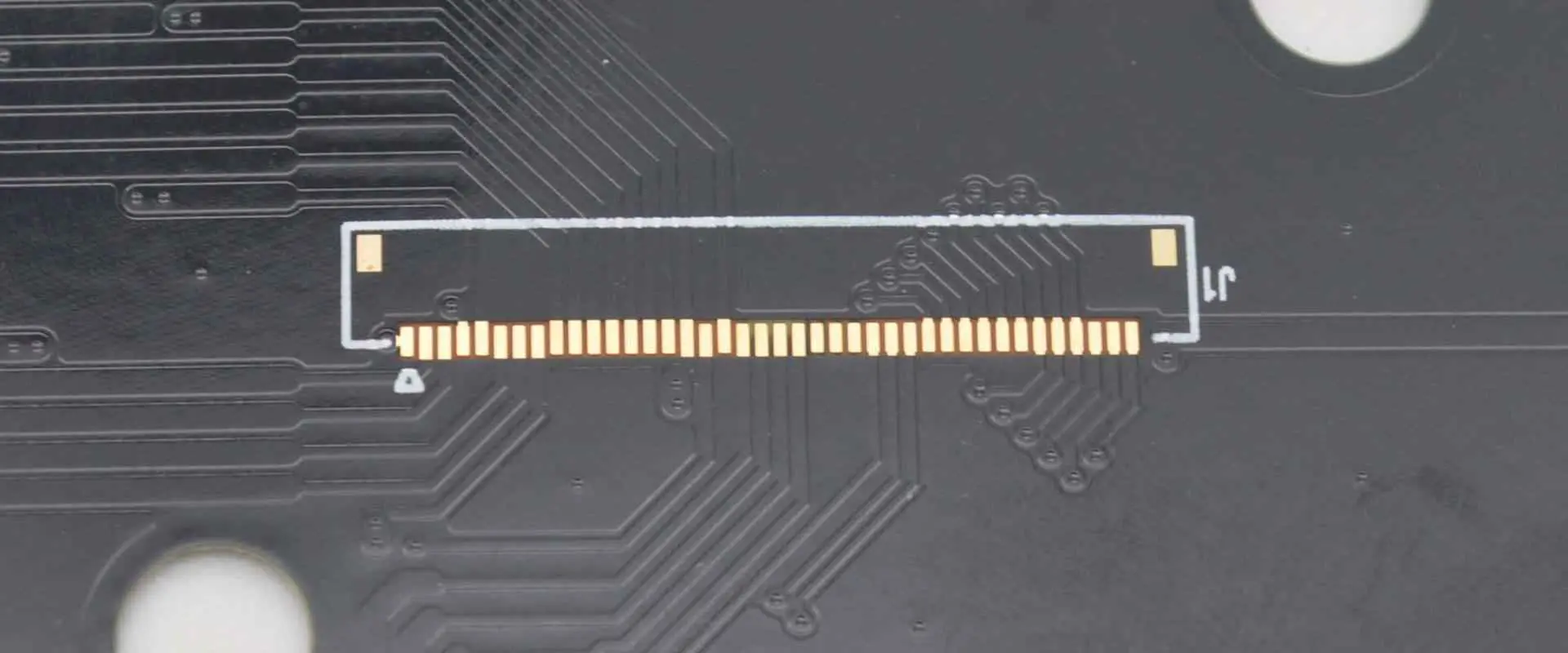
Resistance testing is fundamental in PCB electrical testing. It measures the resistance between various points on the board to ensure that connections are properly made and that there are no unwanted shorts or opens. This test is crucial for verifying the integrity of traces, vias, and other conductive elements on the PCB.

Resistance testing helps in:

  • Detecting manufacturing defects such as broken traces or incomplete vias
  • Verifying the correct resistance values of embedded resistors
  • Identifying potential issues with solder mask or other insulating materials

3. Comparative Testing

Comparative testing involves comparing the electrical characteristics of a PCB under test with those of a known good board. This method is particularly useful when dealing with complex or custom designs where absolute measurements may be difficult to interpret.

Benefits of comparative testing include:

  • Quick identification of deviations from expected performance
  • Reduced need for extensive test programming
  • Ability to catch subtle issues that might be missed by other testing methods

4. Continuity Testing

Continuity testing is a fundamental PCB electrical test that checks for the presence of a complete electrical path between two points. This test is crucial for ensuring that all intended connections are properly made and that there are no open circuits.

Continuity testing helps in:

  • Verifying proper connections between components and layers
  • Identifying manufacturing defects such as broken traces or incomplete plated-through holes
  • Ensuring the integrity of ground and power planes

5. Flip Test

The flip test is a specialized PCB electrical test used to verify the proper orientation of components on double-sided boards. It involves testing the board in both orientations to ensure that components are correctly placed and that there are no issues with mirrored layouts.

Key aspects of the flip test include:

  • Detecting reversed component placements
  • Verifying proper connections on both sides of the board
  • Identifying potential issues with through-hole components

6. Clamshell Testing

Clamshell testing is a method of PCB electrical testing that uses a fixture with two halves that close around the board like a clamshell. This technique allows for simultaneous testing of both sides of the PCB, improving efficiency and reducing test time.

Advantages of clamshell testing include:

  • Faster testing of double-sided boards
  • Improved contact reliability due to even pressure distribution
  • Ability to test boards with components on both sides

7. Adjacency Testing

Adjacency testing focuses on verifying that there are no unintended electrical connections between adjacent traces or pads on a PCB. This test is particularly important for high-density boards where the risk of shorts due to manufacturing defects is higher.

Adjacency testing helps in:

  • Detecting potential short circuits between closely spaced traces
  • Identifying issues with solder mask or other insulating materials
  • Ensuring proper isolation between different circuit sections

8. Flying Probe Testing

YouTube video

Flying probe testing is a flexible PCB electrical testing method that uses movable probes to make contact with specific points on the board. This technique is particularly useful for testing prototype or low-volume PCBs where the cost of a dedicated test fixture may not be justified.

Key features of flying probe testing include:

  • Ability to test complex boards with minimal setup time
  • Flexibility to accommodate design changes without modifying test fixtures
  • High precision and ability to test fine-pitch components

9. PCB Stress Testing

PCB stress testing involves subjecting the board to various environmental and electrical stresses to evaluate its performance under extreme conditions. This type of testing helps ensure that the PCB can withstand the rigors of its intended operating environment.

Common PCB stress tests include:

  • Thermal cycling to simulate temperature variations
  • Vibration testing to assess mechanical durability
  • Power cycling to evaluate the board’s response to repeated on/off cycles

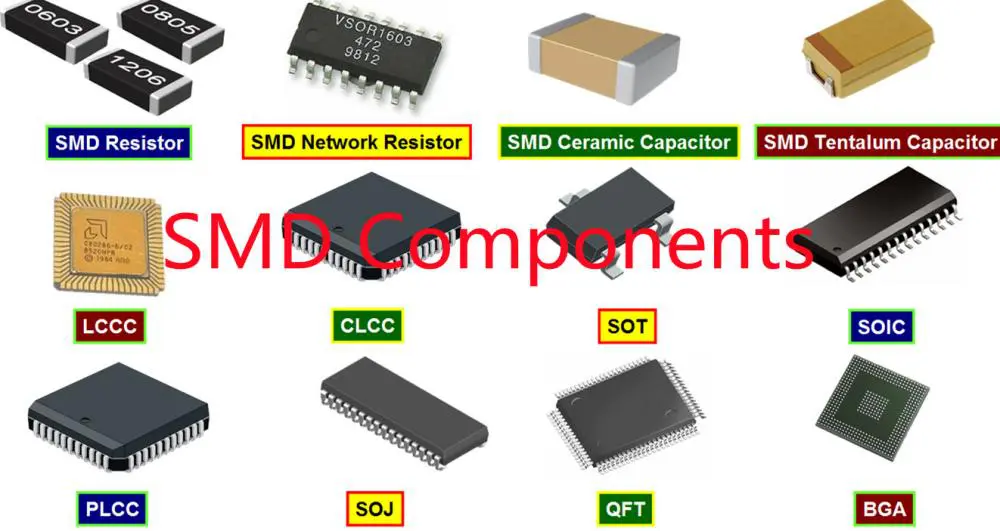
10. In-Circuit Testing

In-circuit testing (ICT) is a comprehensive PCB electrical testing method that evaluates individual components on a populated board. This test uses a bed-of-nails fixture to make contact with numerous test points simultaneously, allowing for rapid and thorough testing of complex assemblies.

Benefits of in-circuit testing include:

  • Ability to test both passive and active components
  • Detection of manufacturing defects such as solder bridges or missing components
  • Verification of component values and basic functionality

11. Functional Testing

Functional testing is the final stage of PCB electrical testing, where the assembled board is evaluated under conditions that simulate its intended use. This test verifies that the PCB performs all its required functions correctly and meets the specified performance criteria.

Key aspects of functional testing include:

  • Verifying proper operation of all circuit functions
  • Testing board performance under various input conditions
  • Evaluating the interaction between different subsystems on the PCB

12. Burn-In Testing

YouTube video

Burn-in testing is a reliability test that involves operating the PCB under elevated stress conditions (such as high temperature or voltage) for an extended period. This test is designed to identify any early-life failures or “infant mortality” issues before the product is shipped to customers.

Burn-in testing helps in:

  • Identifying weak components or manufacturing defects that might lead to premature failure
  • Improving overall product reliability
  • Reducing the likelihood of field failures during the product’s early life

Methods of PCB Electrical Testing

Now that we’ve explored the various types of PCB electrical testing, let’s delve into the methods used to perform these tests. There are several approaches to PCB electrical testing, each with its own advantages and applications.

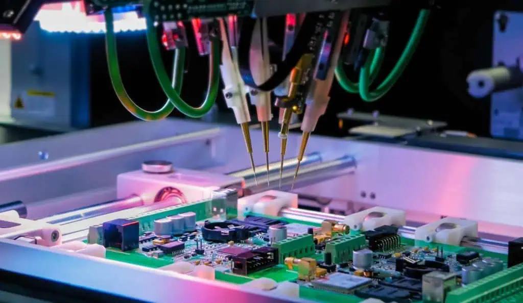
1. E-test Method 1: Flying Probe Testing (FPT)

Flying Probe Testing, also known as FPT, is a versatile and widely used method for PCB electrical testing. This technique employs movable probes that can be positioned anywhere on the board’s surface to make electrical contact with test points.

Key features of Flying Probe Testing include:

  • Flexibility: FPT can easily adapt to different board designs without the need for custom fixtures.
  • Cost-effectiveness: Ideal for low-volume production or prototype testing where dedicated fixtures may not be economical.
  • Precision: Capable of testing fine-pitch components and densely populated boards.
  • Minimal setup time: New boards can be programmed and tested quickly.

The FPT process typically involves the following steps:

  1. Board alignment and registration
  2. Probe movement and contact with test points
  3. Electrical measurements and data collection
  4. Analysis and reporting of test results

While FPT is slower than fixture-based testing for high-volume production, its flexibility and low setup costs make it an excellent choice for many PCB manufacturers.

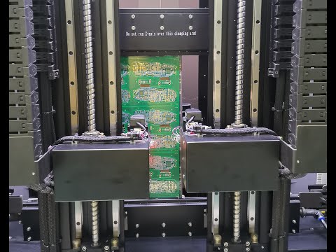
2. E-test Method 2: Fixture Method

The fixture method, also known as bed-of-nails testing, is a high-speed PCB electrical testing technique that uses a custom-designed test fixture with numerous spring-loaded pins (the “nails”) to make contact with specific points on the board simultaneously.

Advantages of the fixture method include:

  • High-speed testing: Ideal for high-volume production
  • Comprehensive coverage: Can test hundreds or thousands of points simultaneously
  • Repeatability: Consistent results due to fixed probe locations
  • Durability: Fixtures can withstand thousands of test cycles

The fixture method process typically involves:

  1. Designing and manufacturing a custom test fixture for the specific PCB
  2. Loading the PCB into the fixture
  3. Applying pressure to ensure good contact between the board and test pins
  4. Performing a series of electrical tests
  5. Analyzing and reporting the results

While the initial cost of creating a custom fixture can be high, this method becomes very cost-effective for large production runs where the setup cost is amortized over many boards.

3. PCB Testing During Manufacturing

PCB electrical testing is not a single-step process but rather an integral part of the entire manufacturing workflow. Testing occurs at various stages to ensure quality and catch defects as early as possible.

Key testing stages during PCB manufacturing include:

  1. Bare board testing: Performed after PCB fabrication but before component assembly
  2. In-circuit testing: Conducted after components are mounted but before final assembly
  3. Functional testing: Performed on the fully assembled PCB

Each stage of testing serves a specific purpose and helps to maintain high quality standards throughout the production process.

4. Mechanical PCB Testing and Inspection

While not strictly part of electrical testing, mechanical testing and inspection are crucial components of overall PCB quality assurance. These processes ensure that the physical characteristics of the board meet specifications and that there are no visible defects.

Mechanical PCB testing and inspection may include:

  • Dimensional verification: Checking board size, hole diameters, and component placement
  • Visual inspection: Looking for visible defects such as scratches, dents, or misaligned layers
  • X-ray inspection: Examining internal layers and hidden solder joints
  • Microsectioning: Analyzing the internal structure of the PCB

These mechanical tests complement electrical testing to provide a comprehensive quality assessment of the PCB.

5. Electrical PCB Testing During Manufacturing

Electrical testing during the PCB manufacturing process is a multi-stage approach that ensures the quality and functionality of the board at each critical step. Here’s a closer look at how electrical testing is integrated into the manufacturing workflow:

  1. Bare Board Testing:
    • Performed after PCB fabrication but before component assembly
    • Checks for opens, shorts, and correct impedance on traces
    • Verifies the integrity of plated-through holes and vias
    • Ensures proper isolation between layers
  2. Component Placement Verification:
    • Conducted immediately after component placement but before soldering
    • Uses optical or X-ray inspection to verify correct component orientation and placement
    • Helps prevent issues caused by misplaced or missing components
  3. Post-Reflow Testing:
    • Performed after components are soldered to the board
    • Checks for solder bridges, cold joints, and other soldering defects
    • May include thermal imaging to identify potential hot spots
  4. In-Circuit Testing (ICT):
    • Conducted on the assembled board
    • Tests individual components for proper values and basic functionality
    • Identifies manufacturing defects such as shorts, opens, or incorrect components
  5. Functional Testing:
    • Performed on the fully assembled PCB
    • Verifies that the board functions as intended under various operating conditions
    • May include power-on testing, signal integrity analysis, and performance benchmarking
  6. Final Quality Assurance:
    • Combines results from all previous tests
    • May include additional environmental stress testing or burn-in procedures
    • Ensures that only fully functional and reliable PCBs are shipped to customers

By incorporating electrical testing throughout the manufacturing process, PCB producers can identify and address issues at the earliest possible stage, minimizing rework costs and improving overall product quality.

Why Electrical Testing Is Crucial and How It Matters to You

PCB electrical testing is not just a technical requirementโ€”it has far-reaching implications for manufacturers, customers, and end-users alike. Understanding the importance of thorough electrical testing can help you make informed decisions about your PCB projects and ensure the success of your electronic products.

1. Quality Assurance

Electrical testing is the backbone of PCB quality assurance. It provides objective data on the performance and reliability of each board, ensuring that only high-quality products reach the market. For manufacturers, this means:

  • Reduced warranty claims and returns
  • Enhanced reputation for reliability
  • Improved customer satisfaction and loyalty

For customers and end-users, rigorous electrical testing translates to:

  • More reliable electronic products
  • Longer product lifespans
  • Reduced frustration from malfunctioning devices

2. Cost Savings

While electrical testing does add to the initial production cost, it ultimately leads to significant cost savings:

  • Early detection of defects reduces costly rework and scrap
  • Fewer field failures mean lower warranty and support costs
  • Improved yield rates lead to more efficient production

These savings can be passed on to customers in the form of more competitive pricing or reinvested in product development and innovation.

3. Regulatory Compliance

Many industries have strict regulatory requirements for electronic products. Comprehensive electrical testing helps ensure that PCBs meet these standards, which is crucial for:

  • Obtaining necessary certifications (e.g., UL, CE, FCC)
  • Entering regulated markets (e.g., medical devices, aerospace)
  • Avoiding legal issues and potential recalls

4. Product Performance and Reliability

Thorough electrical testing contributes to improved product performance and reliability:

  • Identifies potential weak points before they become field failures
  • Ensures consistent performance across production batches
  • Helps in fine-tuning designs for optimal performance

For end-users, this means products that work as expected and continue to perform reliably over time.

5. Time-to-Market

While it might seem counterintuitive, investing in comprehensive electrical testing can actually speed up time-to-market:

  • Catches design issues early in the development process
  • Reduces the likelihood of last-minute design changes
  • Streamlines the certification process

This can give manufacturers a competitive edge in fast-paced markets where being first to market is crucial.

6. Continuous Improvement

The data gathered from electrical testing is invaluable for continuous improvement efforts:

  • Identifies trends in manufacturing defects
  • Provides insights for refining design guidelines
  • Helps in optimizing production processes

For customers, this ongoing improvement translates to ever-increasing product quality and reliability.

PCB Electrical Testing at RAYMING PCB

At RAYMING PCB, we understand the critical importance of thorough and accurate electrical testing in the PCB manufacturing process. Our state-of-the-art testing facilities and experienced technicians ensure that every board we produce meets the highest standards of quality and reliability.

Our Comprehensive Testing Approach

  1. Advanced Testing Equipment:
    • We utilize cutting-edge flying probe testers for flexible, high-precision testing
    • Our bed-of-nails fixtures provide rapid, comprehensive testing for high-volume production
    • Thermal imaging and X-ray inspection systems complement our electrical testing capabilities
  2. Customized Testing Solutions:
    • We develop tailored testing protocols based on your specific PCB design and requirements
    • Our engineers work closely with you to identify critical test points and parameters
  3. Multi-Stage Testing:
    • We perform electrical tests at every crucial stage of the PCB manufacturing process
    • From bare board testing to final functional verification, we ensure quality at every step
  4. Data-Driven Quality Assurance:
    • Our advanced data analytics help identify trends and potential issues before they become problems
    • We provide detailed test reports with each order, giving you complete visibility into the quality of your PCBs
  5. Continuous Improvement:
    • We regularly review and update our testing procedures to stay ahead of industry standards
    • Our team undergoes ongoing training to maintain expertise in the latest testing methodologies

What is FR4 Tg PCB?

Isola FR406N PCB

As electronic technology continues to develop, there is a high demand for high Tg boards.Furthermore, glass transition temperature (Tg) is a very important property of an epoxy. Also, this temperature region is one whereby the base material, which is either glass or polymer changes from its glassy, rigid, solid state into a rubbery state.

All PCB features a unique Tg value which is usually based on the substrate. Furthermore, PCB will begin to alter its state. This affects the PCB fabrication process wrongly if the PCBโ€™s operating temperature surpasses its Tg value. In addition, the PCB boards with high Tg usually feature better stability whenever there are high temperatures. This is due to the fact that the substrate offers better chemical and mechanical stability, and heat resistance for the board.

Therefore, your Tg value must fall within 20 and 25 degrees centigrade more compared to the operating temperature of that device expected for the board to be useful in selecting a PCB.

What Does FR4 Mean?

Printed circuit boards usually make use of composite material glass fabric as well as a flame retardant made of epoxy resin.

This reinforcing material of 4th grade is useful in PCB boards to help in resisting a more glass transition temperature. Also, the presence of this substrate in the PCB is significant, such as printed circuit boards (PCBs) present in the electrical machines.

FR means fire retardant material. Majority of PCB manufacturers make use of FR4 as a result of its consistent mechanical and physical properties. In addition, the FR4 laminates are board materials with epoxy pigment useful in enhancing the integrity of the circuit board.

What does High TG PCB Mean?

Base material, either glass or polymer, is shifting from its rigid, solid, glassy state to a rubbery state whereby the temperature rises to a specific area. The temperature here is referred to as the glass transition temperature(Tg). What we mean is that Tg is known as a mechanical property, which designates the glass transition temperature. This temperature is one at which this substrate stays rigid.

What are the Properties of the Fr4 Tg PCB?

FULL PCB MANUFACTURING Quote

The use of materials of high Tg PCB is becoming higher in the global electronics industry. The usefulness of these high Tg PCBs can be seen in communication equipment, control panels, and computers.

The major difference here is the high prices. This is because these high Tg fr4 PCBs are more expensive than the usual Tg PCBs. Furthermore, these high Tg material feature most of the important properties. These include:

  • Adhesion
  • Better strength and mechanical property
  • Stronger moisture resistance and water absorption
  • Stability in its dimensions
  • Thermal decomposition during any hot condition
  • Chemical resistance
  • High heat resistance or higher heat resistance
  • More resistance to any thermal stress
  • Longer durability for the PCB laminates
  • Reliable and efficient PTH
  • Lower CTE (coefficient of thermal expansion) at the Z-axis

What are the Benefits of a High Tg PCBs?

Greater stability: This automatically improves the chemical resistance, heat resistance, moisture resistance, temperature resistance and the deviceโ€™s stability by raising the temperature of glass transition (Tg) of a specific PCB substrate.

It bears designs with high power density: A high Tg PCB serves as a very good solution for all heat management. This holds if that device features high power density as well as a high heat generation rate.

Also, with the use of the larger PCB (printed circuit board) in changing a deviceโ€™s power and design requirements when reducing an ordinary boardโ€™s heat generation. In addition, it can also make use of high Tg PCB (Printed circuit board).

Great for HDI and multilayer PCBs: This can cause high heat dissipation levels. This is due to the fact that the HDI and multilayer PCBs feature dense circuits and are usually more compact. Therefore, the high Tg PCBs are usually useful for the HDI and multilayer PCBs. This ensures reliability during PCB fabrication

Reasons why Using the high Tg PCB is Necessary

Note that if yourPCB (printed circuit board) canโ€™t bear the thermal load that is not having a Tg value that is 25 degrees centigrade less than the usual Tg, then there is a need for a high Tg PCB (Printed circuit board)to work with your applications.

Furthermore, it ensures the safety with your high Tg PCB if the product operates at a range of 130 degrees centigrade or more. The major reason behind the high Tg PCB is due to the movement onto the RoHS PCB (Printed circuit board). Therefore, there are additional PCB industries that are moving toward the high TG materials because the lead-free solder needed to flow will require higher temperatures.

What are the Applications of High Tg FR4?

Note that when a higher power density is present in electronic products and then heat generation also tends to disturb the heat sink as well as other parts of your products, the most appropriate solution is to using a high Tg FR4 PCB.

Furthermore, youโ€™ll learn that the high Tg FR4 PCBs are usually applied in the electronic industries. These industries can function in high temperatures This is because high Tg FR4 PCB are becoming more popular recently. Top manufacturers like RayMing serve their customers from many different industries. They achieve this by offering high Tg FR4 PCBs having a heat resistance, which meet all the demands as well as the specifications of the customer in the quick lead time.

The following areas are places where the High Tg fr4 is applicable:

  • Rfid
  • Gateway
  • Antenna
  • Inverter
  • Embedded systems development
  • Contract manufacturing services
  • WiFi Booster
  • Low Cost Plc
  • AC power supplies
  • Embedded Computer Systems

Conclusion

When designing, one important feature to look into when identifying PCBs is the high Tg. Furthermore, it is necessary to pick the material with respect to the usage. This refers to the low working or high temperature requirements. Other things to consider include the thermal expansion, electrical properties, temperature resistance, mechanical and electrical properties, high temperatures, and higher heat resistance or high heat resistance. Any questions? Please notify us.

How BT PCB is Contributing to the Advancement in Electronic Equipment

bt pcb

BT stands for bismaleimide triazine. This laminate sheet has impacted the chip packaging industry. Chip packaging is crucial in PCB assembly. Laminated materials for circuit boards usually comprise several layers of impregnated and dried glass fiber cloth pressed onto the chip substrate. However, a thermal-hardened bismaleimide triazine (BT) resin material was introduced. This material offers great electrical and thermal properties and is low cost.

BT resin laminate has been playing a crucial role in the development of electronic equipment and information technology.

What is a BT PCB?

BT stands for bismaleimide triazine. ย It is one of thermoset resins utilized in manufacturing PCBs. Also, this component is a primarily a mixture of epoxy resin and BT resins. The epoxy resin is a common raw material used for PCBs. Also, the BT resins are majorly a mixture of bismaleimide, used as a common raw material for circuit boards and cyanate ester. BT resin is a combination of strongly basic molecules.

BT resin features great properties like excellent electrical properties and high thermal resistance.  These features increased the standard for high-performance semiconductors. Also, the low cost of BT laminate makes it an ideal option for chip packaging. Therefore, BT laminate is contributing to technological advances for electronic devices.

To date, BT laminate remains a good standard for chip packaging. Before the introduction of BT laminate, the laminate used for high-performance chips was high-cost ceramic. However, BT became an alternative with great electrical and thermal properties. When the chip manufacturing industry noticed this material, the BT resin was used for chip packaging in 1985.

This material became to gain acceptance in Japan and across the world when the chip manufacturing industry accepted the cost savings. Furthermore, BT resin made the chip fabrication process much simpler. To date, BT resin is a popular laminate material for chip packaging. BT PCB is a mixture of epoxy resin and bismaleimide.

Applications of BT PCB

Any devices featuring electronic components feature one or more computer chips. Device makers constantly look for how to make their products better by making them lighter and smaller. Also, they make these devices more sophisticated.  An example of this is the smartphone technology that keeps evolving each model while becoming more powerful, lighter, and more versatile.

The manufacturers of the chips in these devices keep improving their chip technology to meet the demands of manufacturers for advanced functionality. Also, chip manufacturers need to put more parts into a chip to make devices lighter and more efficient. Therefore, these manufacturers make use of denser materials that can reduce spacing between the traces.

Spacing of traces has reduced from more than 100 microns to less than 20 microns. Furthermore, the greatest challenge during PCB fabrication is avoiding curvature or deformation caused by temperature variation. Also, PCB fabrication involves processes that alternate cold and hot. Therefore, the chip must comprise materials that must keep their shape in these conditions. The bismaleimide triazine resin is a low cost material that features high performance in all aspects.

Also, chips function under conditions with incessant contraction and expansion. Therefore, they must be able to keep their performance specifications without any form of degradation throughout their life span. The bismaleimide triazine resin is a primary material in chips that function in electronic devices of today.

Also, the complexity of todayโ€™s technology keeps demanding for a dramatic revolution in the semiconductor industry. Bismaleimide triazine resin is the breakthrough these technologies need. Therefore, the industry keeps improving BT laminate and anticipating the future demands of chip makers.

Properties of BT Epoxy

BT epoxy is widely used in fabricating printed circuit boards due to their exceptional electrical and mechanical properties. Also, BT features excellent thermal properties. This laminate is ideal for lead-free PCB assembly. Also, BT epoxy resin is primarily used in multilayer PCB applications. BT epoxy offers great features like high heat resistance, exceptional electromigration, and insulation resistance.

Furthermore, BT epoxy features high bond strength at extremely high temperatures. BT epoxy resin is widely used across several industries since they offer a great level of protection.  BT epoxy is listed in some standards in the world due to its properties.  For example, IPG4101-1997 listed it as โ€œNo. 30โ€ board while EC 249-2-1994 listed it as โ€œ18โ€ board

In addition, BT epoxy features a high glass transition temperature and low dielectric constant. Therefore, BT resin substrate can improve the interconnection of printed circuit boards. BT stands for Bismaleimide triazine. This common raw material features low thermal expansion and exceptional dielectric properties. Therefore, this makes it ideal for high-density interconnect (HDI).

The properties of BT epoxy includes:

  • Exceptional thermal shock resistance
  • Great ion migration resistance
  • Exceptional dielectric performance, Dk is within 2.8 and 3.5
  • Great electrical properties
  • Excellent dimensional stability and curing shrinkage
  • Good wettability and low melt viscosity

Factors that Determine the Performance of BT PCB

BT resin as a common raw material for PCB fabrication varies from low-viscosity liquid to solid based on the ratio and variety of CE and BMI. There are several factors determine the performance of BT PCB. These factors include:

Development of lead-free soldering technology

The majority of PCB manufacturer integrate led-free soldering technology. This has become the mainstream of the industry. Higher temperature reflow soldering related with this technology will put more heat resistance requirements on PCB production.

Packaging technology development

Traditional semiconductor packaging products like DIP and QFP should connect the chip to the lead frame and utilize gold wire to link the aluminum pad on the chip. The utilization of organic substrates with internal pin, connection PBGA, EBGA, and packaging methods like TAB are increasing. Also, many new technologies like WLSCP, CSP, and chip packaging soil are increasing as portable products need component volume miniaturization.

High frequency

The information and communication technology has enhanced its working frequency. For instance, mobile phonesโ€™ standard has evolved over time. Also, the operating frequency of the CPU has changed over time. The emergence of different digital communications and the development of MHz and now GHz  are part of the development.

Conclusion

BT PCB is highly preferred among electronics manufacturers due to its electrical and mechanical properties. Also, the low cost of BT laminate makes it an ideal option for chip packaging.

How 5G IoT is Changing the Future of Technology

5G IoT Technology

5G has brought several new possibilities for businesses and enterprises that require faster data and more efficiency. The impact of 5G in the technology world and the whole world at large has become so evident. With the increasing production of more advanced electronics, there is need for faster signal transmission and data transfer.

5G is presently available in most cities in the developed world. With 5G, a lot of IoT applications and devices will be connected easily. 5G Internet of Things supports new business models. The mobile communication system has experienced a lot of development in the past years. This system has seen the transformation from 2G to 3G to 4G and now 5G.

In this article, we will provide answers to questions like what is 5G IoT and how exactly does 5G offer greater data speeds?

What is 5G?

5G refers to the fifth-generation cellular technology that enables new capabilities like cloud computing, Internet of Things, Artificial Intelligence, and Edge computing. There are several factors that trigger the integration of 5G and IoT. Some of these factors include the availability of affordable devices and the rising demand from enterprises and consumers.

In addition, the adoption of global standards is driving growth and increasing market interest in the Internet of Things. Edge computing, AI, and cloud computing can handle the volumes of data produced by the IoT. Furthermore, 5G advancements like 5G core and network slicing will help to achieve the goal of a global IoT network.

The transformation in the digital world is basically changing businesses and the society at large. Also, it is changing our daily lives. Mobile networking is the brain behind this transformation. Also, mobile networking offers reliable and global connectivity to over 6 billion mobile devices. 5G is also responsible for high computing power in modern devices.

How Does 5G Benefit IoT?

5G offers many benefits for Internet of Things. Also, faster connection of things can help enterprises and businesses to develop new products or improve existing ones. Furthermore, the impact of IoT keeps growing as it transcends almost every industry like smart manufacturing and utilities, automotive. In addition, Internet of Things will keep benefiting the society at large by enabling government policy implementation.

By enabling the reduction of waste of critical resources like water, the initial mobile networks such as 2G, 3G, and 4G offer the basic foundation for connecting things. These mobile networks were initially designed to ensure mobile broadband and personal communication services. However, they have provided the capability to meet the demands for IoT. Also, they offer technical capabilities beyond most existing use cases.

For instance, global standardization indicate that services and products can be globally scaled. With billions of connected mobiles, there will be reliability, cost efficiency, and the constant development of devices.

Therefore, 5G offers the following key benefits for IoT

  • Faster data in local and urban areas networks
  • Improved mobile broadband
  • Enhanced energy saving functions for indoor devices
  • Very reliable low latency communications
  • Better connectivity for the internet age in rural places

5G is now available across the globe. Also, this 5th generation mobile network is specially designed to support IoT use cases. Therefore, 5G offers dedicated capabilities designed for different kinds of IoT applications. 5G enables the development of new IoT applications. Also, this cellular technology will keep fueling digital transformation. Therefore, this will benefit consumers, enterprises, and the society at large.

Also, 5G offers several benefits to the mobile industry. The mobile communications industry depends on 5G IoT. In addition, 5G helps to ensure efficiency and reliability in most IoT projects.

How 5G Evolution Creates New Opportunities in IoT

As 5G becomes more available, it will offer support to mission critical Internet of Things. This is possible due to the low latency and higher bandwidth provided by 5G. Therefore, this will ensure future use cased like automated guided vehicles, assisted driving, connected devices, and more. Also, it is still not clear how 5G will be needed at the upgrade path to offer support to IoT use cases that require continuous high-speed communications.

5G will offer several new possibilities for business and enterprises that require faster and more efficient data. Also, 5G can address several use cases that require a lot data like video streaming. 5G is available in major cities. In large parts of Europe, this cellular technology will replace both 2G and 3G. The replacement of 2G and 3G with 5G in many European countries is a mainstream reality in the year 2025.

Furthermore, 5G will help IoT applications to gain more remote control. For instance, NB-IoT and LTE-M will enable network functionality that ensures improved coverage or minimized battery consumption for an application. 5G enables mass deployment for simpler and more efficient IoT devices, like sensors. Also, these devices transmit little data. However, energy efficiency, cost, and better coverage can be crucial for relevant use cases.

5G enhanced mobile broadband offers more data. Also, it improves data security. Therefore, it offers fast response which can be widely used collaborative robots and autonomous vehicles. Network edge in IOT project is crucial.

5G Development Stage from an IoT Application Perspective

For the past few years, 5G deployment became rapid in several markets across the world. Also, mobile phones with 5G capability have become more affordable. Therefore, this enables mobile broadband users start gaining 5G benefits where available. This situation is kind of different from an IoT application perspective.

For instance, several IoT use cases require continuous network access. This means the application requires optimizing networks having sufficient coverage. It is crucial to think ahead when it comes to IoT applications. This is because the decision made today will affect the cost and capabilities of the connected devices for several years.

From the perspective of an IoT application, it is better to view the road to 5G in three stages. These stages are transition, evolve, and transform.

Transition stage

FULL PCB MANUFACTURING Quote

5G introduction will be more than a 10 year period. Every network generation needs to be well standardized to enable global interoperability. Also, the regulator in every country plans the award licenses to utilize it. Furthermore, communication service providers need to operate the new network and perform roll outs.

It is a lengthy process when rolling out a new mobile network. Also, it takes years for a new network generation to accomplish the same coverage as the preceding generations. This transition stage will last until the new network offers enough coverage to eliminate dependency on legacy networks. Also, when it comes to international IoT applications, this stage may last until all countries have enough coverage.

The roll-out time for 5G will vary for different use cases. For instance, big mobile IoT capabilities such as NB-IoT and LTE-M are well optimized for a better coverage. IoT application must rely on multiple networks generation to get enough coverage. Therefore, this means the application canโ€™t enjoy full benefit of new network capabilities.

Evolve stage

It will be feasible to start indicating the first benefits from new capabilities as 5G network coverage is sufficient. The demands of the application determine the type of coverage needed. For instance, an application where the communication information isnโ€™t time critical needs less coverage than applications with near real-time characteristics. Based on the location, IoT use cases will get to this stage between now and 2025.

Physical connectivity is one of the first benefits of 5G. Device cost for applications having strict cost requirements will reduce once we eliminate fallback technology and make use of 5G. Also, this can allow new applications that have not been feasible economically. With the help of other 5G characteristics, new and improved applications can be also designed.

As economical and technical limitations relax, there will be more opportunities to innovate new applications. With 5G devices, the feasibility of bringing an โ€œalways-onโ€ user experience for IoT devices is high. Also, 5G technologies make it easy to simplify modern architecture and prepare it for more transformation change.

In several cases, one can directly attach sensors to the mobile network. This helps to enhance operational characteristics.

Transform

IoT application must enable the appropriate characteristics of the network infrastructure to enhance business. For instance, there may be a need to assure response times and data rates. Also, 5G helps the application to see the networkโ€™s capabilities. This enables 5G to support the specific needs of the network by programming it.

Furthermore, this can only work when the desired capabilities are already deployed in the network having enough coverage. It isnโ€™t an easy task to accomplish the vision of 5G. Achieving this vision can take years. However, there are new practical uses cases and more capabilities. Also, accessing low power consumption and improved coverage capabilities is now possible. Therefore, this has paved way for more new use cases.

Furthermore, IoT service providers across the globe are incorporating access to such functionality. The accessibility of 5G capabilities for development project must have been integrated into the services and software used for the application. Furthermore, 5G will result in a long period of transformation in the mobile IoT ecosystem.

Therefore, enterprises that look forward to transforming their business should opt for partners that can support business-critical processes.  Focusing on business challenges and developing the IoT system plays a key role in the future.

5G IoT Use Cases

There are several use cases of 5G IoT. These uses cases include:

Manufacturing

Industrial companies are already leveraging the Industrial IoT to keep track of the location of these assets. With 5G IoT, it is easy to develop smart factories with robotics and AI. The ultra-reliable low-latency 5G helps to reveal transformative use cases in manufacturing and infrastructure systems.

Smart traffic mobility

5G IoT applications can ensure real-time data is shared about road and traffic conditions among road users. This driver assistance services and smart mobility need 5G communication devices in roadside sensors and vehicles. Also, gathering and analyzing real-time  IoT data from vehicles and roadside infrastructure help to warn drivers about any hazardous road conditions. Therefore, traffic efficiency and road safety will improve.

Video survelliance

5G has ensured digital transformation in our todayโ€™s world. One of the IoT applications 5G has enhanced is the video surveillance. The recent events across the globe has triggered governmentโ€™s investment in security systems and public surveillance. Also, video surveillance systems often depend on wired  connectivity.

However, the integration of wireless connectivity can lead to lower costs, providing reliable connectivity and performance. 5G and IoT solutions prevent critical assets loss. With 5G, we can secure and monitor facility conditions properly.

Smart city

According to the European Commission, Smart cities are where traditional services and networks are more efficient with the integration of telecommunication and digital technologies. Smart cities utilize the 5G and IoT devices to gather real-time information. Therefore, this helps to understand the patterns of demands and respond with lower-cost and faster solutions.

Furthermore, 5G will reveal IoT potential and this will be a driving force for smart cities. It will achieve this by addressing and providing solutions to all connectivity issues.

Smart grid automation

Electricity demand is rising. Smart grids and virtual power plants are solutions for this rising demand. With 5G, we can integrate real-time management and ensure smart electricity grid automation. Maintenance optimization can begin once fault is detected. 5G IoT is widely integrated due to the lower latency and increased deployment rate.

Therefore, utility operators are gradually updating their grids with new control systems. Also, smart grid automation can help to get rid of blackouts across the world.

Asset tracking

Remote monitoring with IoT is not new. However, using 5G to secure connectivity helps to deliver great benefits. Asset tracking solutions transmits data from a sensor to the cloud for storage and analysis. 4G LTE networks are compatible with 5G. For instance, NB-IoT is the brain behind 5G massive-Type Communications. The mobile industry requires asset tracking to ensure efficiency.

Remote working and studying

5G has enabled remote studying and working. Improved mobile broadband will allow more mobile data at once. 5G can enable devices with more efficient hardware require a long battery life. Also, longer battery life indicates that devices can transmit data on their location for a long period. The internet is critical in keeping the society connected. An example of this is was the COVID-19 lockdown. During lockdown, remote working and studying became the order of the day.

Conclusion

The impact of 5G in the technology world and the whole world at large has become so evident. Also, there are several use cases of 5G IoT.

Why you Should Use TTM PCB for Your PCB Projects

Shengyi SG7350D PCB

In the technology world, various companies are working towards development. These companies offer high quality services and products. One of such companies is TTM Technologies .Inc. This company is well-known for its positive impact in the PCB industry. We are going to shed more light on the products and services provided by this company. Also, we will give more details on how they operate.

What is TTM Technologies .Inc?

TTM technologies, is a popular and leading global printed circuit boards manufacturer. Also, this leading global printed circuit board manufacturer focuses on delivering quick-turn and high volume production of technically advanced circuit boards. TTM stands or refers to โ€œfor time to market.โ€ Also, TTM Technologies .Inc specializes in manufacturing RF components.

TTM Technologies Inc. has its headquarters in Santa Ana, California. Also, the major focus of this manufacturer is time-to-market. With its advanced technologies, procedures, and services, customers can reduce the time needed to make their advanced electronics available. TTM technologies .Inc dedicates its time to production of advanced circuits, RF and microwave components, and backplane assemblies.

This company is one of the worldโ€™s biggest PCB producers and a large supplier of custom electro-mechanical solutions and backplane assemblies. Also, it offers one-stop manufacturing services that help to shorten production time.   The time-to-market reveals TTMโ€™s time-critical.

TTM Technologies .Inc offers all types of PCB boards like rigid-flex, flex, HDI, and rigid. Also, it offers up to 40 layers circuit boards. This competitive organization works with a team of experienced engineers that offers customers the necessary advice and support. also, TTM Technologies is dedicated to meeting the needs of its customers by continuously improving product quality and customer service.

More Facts about TTM Technologies .Inc

FULL PCB MANUFACTURING Quote

TTM Technologies deals with the manufacturing and sale of printed circuit boards across the world. Also, TTM Technologies. Inc operates in two different segments which are RF components and PCB. This company offers

  • Radio frequency and microwave circuits
  • PCB products
  • Conventional PCBs
  • High density interconnect (HDI) PCBs
  • System integration products
  • Advanced ceramic RF components
  • Radio frequency components
  • Beamforming and switching networks
  • Multi-chip modules

Furthermore, this company manufactures circuit boards with heavy copper cores. Also, it produces electrically passive heat sinks and circuit boards with active thermal cores. TTM Technologies .Inc delivers value added services which include PCB layout design, quick turnaround, and design for manufacturability. Also, it offers services like simulation and testing.

TTM Technologies .Inc has its headquarters in Santa Ana. This company acts as electronic manufacturing services companies and original equipment manufacturers. Therefore, TTM Technologies .Inc serve data center computing, medical, aerospace and defense sectors.

As a leading global printed circuit board manufacturer, TTM Technologies .Inc manufacturing services enable customers to achieve the best PCB project. Also, this company features design capabilities to produce technologically advanced PCBs. This leading global manufacturer has huge net sales. TTM Technologies .Inc delivers specialty components for electronics manufacturing. Also, it delivers high frequency radio frequency components.

TTM stands for time to market. Therefore, TTM Technologies .Inc offers high volume production, quick turn, and one stop manufacturing services. TTM technologies .Inc has more than 21 years experience in technology. Therefore, TTM Technologies .Inc keeps working towards meeting the goal of change and technology advancements. TTM Technologies .Inc in Santa ana California reports fiscal records annually.

The Engineering Fields of TTM Technologies

TTM Technologies .Inc works with more than 2,000 technical professionals and engineers. Therefore, it achieves great goals through continuous improvement, design and development. TTM Technologies .Inc features the following fields:

RF/Microwave engineering

The engineers in this field specialize in designing and evaluating, integrated microwave assemblies, and sub-systems. Also, this engineers use PWB SMT, advanced packaging techniques, chip and wire in this field.

Field application engineering

In this field, the engineers offer technical support and advice to customers. Also, they offer support to manufacturing groups and PCB designers. Engineers here interface with the groups involved in the design cycle and offer feedback on mechanical and electrical demands based on the end product application of the customer.

Process engineering

This field in TTM Technologies .Inc is responsible for maintaining and implementing the production processes utilized to fabricate circuit boards. Also, these processes could include establishment of operating conditions, failure analysis, and regular monitoring of process conditions.

The Financial Outlook of TTM Technologies

The net income of TTM Technologies .Inc for the first three months of 2022 amounted to $25.3 million on a non-GAAP basis. Also, in the first quarter of 2021, this company had a net income of $25.3 million. In the first three months of 2022, the adjusted E BITDA was $62.0 million. This is more than the $61.0 million realized in the first quarter of 2021.

At a conference call, TTM Technologies .Inc made high revenues and non-GAAP earnings beyond the mid-point of the guided range. The strength of the commercial end markets of this company contributed to this outperformance. Despite the production and labor problems in North America, TTM Technologies .Inc was able to achieve this.

Also, the CEO of TTM Technologies .Inc claims that the company took some steps to improve its differentiation strategy. This company agreed to get Telephonics Corporation which delivers engineered solutions for Defense and Aerospace end market. Therefore, TTM technologies .Inc could move up the value chain.

TTM technologies .inc has announced its plans to build a new manufacturing facility in Malaysia. The new facility will help customers in markets like data center computing, industrial, and networking. Also, this new facility will offer TTM Technologies .Inc with more growth vector. This is because TTM Technologies .Inc will attract more demand from existing and new customers in need for technologically advanced PCBs manufacturers outside China.

Therefore, TTM Technologies .Inc will be able to provide customers high layer count and high volume PCBs. According to estimates, the revenue for the second quarter of 2022 will be around $620 million. Meanwhile, the non-GAAP net income was estimated to be between $0.30 to $0.36.

The new facility will take up about $130 million. Also, this investment will spread through 3 years.

Applications of TTM Products

TTM printed circuit boards and other technical products are widely used across industries. Also, this company offers high-quality PCBs, RF and microwave, and more.

Automotive

TTM Technologies .Inc is a great supplier of advanced technology and high reliability PCBs to the automotive industry. Also, automotive electronics manufacturers rely on the products of this company. TTM technologies .inc supports full range of the PCB needs of its automotive customers.

Cellular

TTM Technologies .Inc is a leading supplier of PCBs used in mobile phones. Also, TTM Technologies .Inc  has been able to bring the power of computing and world-wide communication to the palm of your hand. With its leading technology in flexible circuits and advanced HDI, TTM has made major contributions to the mobile phone industry. Also, TTMโ€™s cost efficient production makes it a global leader in the smart phone industry.

Aerospace and defense

As the largest PCB manufacturer in North America, TTM Technologies .Inc has made significant contributions to the aerospace and defense industry. Also, this company delivers custom assemblies to the Aerospace and Defense industry.

Great reliability and exceptional performance are a major concern for military and aerospace electronics. Also, these electronics need to function under the most extreme conditions. Therefore, military and aerospace electronics manufacturers lay more emphasis on the products used for these devices.

RF/microwave

California TTM Technologies .Inc is one of the largest suppliers of Microwave and RF components. Also, these components are widely used in the communications industry. Furthermore, telecommunication devices need high signal integrity to function. The microwave and RF components of TTM Technologies .Inc ensure high signal integrity and minimize signal loss in telecommunication devices.

 TTM technologies .Inc offers products and services that enable satellite communication systems and GPS devices.

Benefits of Choosing TTM Technologies .Inc

There are several PCB companies in the world. However, some companies stand out among others. One of such companies is TTM technologies. Inc. Also, this leading global manufacturer offers electro mechanical solutions and one-stop manufacturing services. TTMโ€™s time critical is one of the reasons behind its quick-turn PCB services.  Below are benefits you will enjoy when you choose TTM Technologies .Inc.

Quality products and services

TTM technologies .Inc offers quality PCB products and PCB one-stop manufacturing service. Also, this company provides high volume production and quick turn services. TTM Technologies .Inc integrates state-of-the-art technologies and procedures when manufacturing circuit boards. It manufactures products like PCB products, conventional PCBs, and high density interconnect (HDI) PCBs.

Great customer service

One of the benefits you will get to enjoy from TTM Technologies .Inc is its great customer service. This PCB manufacturing company ensures it offers support and advice to its customers. Also, TTM Technologies .Inc prioritizes the demands of its customers. Its manufacturing services enable customers to get the best.

Great reputation

California TTM Technologies has built a great reputation in the printed circuit board industry. This company has more than two decades of experience in delivering quality PCB products and services. Also, this company carries out market research and competitor analysis before commencing production.

Conclusion

TTM Technologies .Inc has continued to impact the electronics and PCB industries. This global PCB company has set a great standard for PCB manufacturing. With its headquarters in Santa ana, California, this company is a global designer of PCBs.

Top 10 Analog IC Design Companies in China

Analog IC DESIGN COMPANY

China is the world’s largest manufacturer, builder, and exporter of electronics and electrical equipment. China has seen a boom in the electronics industry in the last few years. That’s because the United State-China trade war has given China a competitive edge. With tariffs on imported goods and new homegrown companies, Chinese manufacturers can offer attractive products at prices that American companies cannot match.

In this article, we will examine the key factors that influence the success of Chinese analog IC producers. This market will grow to over $80 billion by 2023. However, Chinese analog IC producers are foundries that resell their ICs to electronic systems manufacturers. Foreign firms are still reluctant to build state-of-the-art fabrication facilities in China because of the lack of consistent intellectual property (IPR) protection.

The Chinese analog chip market is booming, but local design houses are still far behind international counterparts. For instance, Chinese analog companies can’t match the parameters of their international counterparts’ products because they don’t have access to advanced process technologies. To overcome this problem, analog companies should work closely with the foundries and develop a relationship with them. The supply chain in the electronics industry is tight and foundries prioritize strategic clients.

Demand for automotive chips has spurred manufacturers to relocate production to the country. The chip industry is highly dependent on China for sales, which has resulted in booming sales in the country. China alone accounts for almost 60% of Qualcomm’s revenue globally. The company also got fined USD 1 billion by the Chinese anti-monopoly agency for overusing its dominant position in the country.

Chinese IC producers are foundries that re-sell their ICs to the electronic system producers

 Analog IC

IC production in China may not reach 70% of domestic demand by 2025. IC Insights projects that the country will be responsible for 19.4% of the global IC market by 2025, up from 10.2% in 2010. Last year, Chinese foundries produced a total of $12.3 billion worth of ICs, accounting for a 16.7% global market share. By 2026, this number could reach $183 billion.

China’s foundry sector has made strides in some lagging technologies. In 2018, Chinese foundries fabricated 45 nm and 65 nm semiconductors, which are useful in consumer electronics. Since then, there has been establishment of a few 6-inch and 8-inch fabs. The government also drives demand for these products, prioritizing autonomy over profit. China’s pure-play foundry market grew 41% last year, corresponding to a 19% global market share.

Chinese IC foundries are becoming more competitive in leading-edge technologies

A growing number of Chinese companies are gaining market share in the semiconductor industry. The country is a leader in logic semiconductors, such as CPUs and graphics processing units, but it also produces specialized semiconductors, such as field-programmable gate arrays (FPGAs). However, domestic Chinese companies currently hold only modest market shares. More engineers will be required to achieve the Chinese government’s ambitious goals.

The IC industry started like a poker championship, with hundreds of players paying entry fees and making the most money at the advanced nodes and leading edge. The IC industry has winners and losers over the past couple of decades, but now there are only four remaining players. TSMC has several high-end customers for its 7nm process and supports older generation processes, such as 180nm.

SG Micro Corp

SG Micro is a leading company in high-performance and quality analog IC design. The company introduced more than 350 analog IC products globally, including advanced consumer and medical applications, automotive applications, and energy-efficient power management solutions. Its product range includes voltage regulators, op-amps, and monitoring ICs. Besides high-quality products, SGMICRO is also aiming at production of environmentally-friendly products. The company offers the most reliable customer service, thanks to its experience and quality control.

Founded in the early part of this century, the company’s immediate market is the domestic makers of electronic equipment. Nonetheless, it has begun to attract the attention of international players, especially after it claimed that its power management ICs are part of Qualcomm’s reference designs and MediaTek. Other ICs that SG Micro is having success with include audio line drivers, video buffers, load-switch and reset ICs.

The Global Automotive Analog IC Market Report is a valuable industry information source. It offers in-depth analysis and forecast for the Analog IC industry. The report highlights each industry segment’s market size, share, and growth. It also includes detailed product and revenue forecasts by application and type. With this information, you can determine your position in this market. And, once you’re ready to make the necessary moves to take advantage of market opportunities, SG Micro Analog IC has the expertise and the experience to help you succeed.

COVID-19

A COVID-19 outbreak began in December 2019 and spread to all parts in the world. As a result, the World Health Organization declared it a public health emergency. This situation has already had a global impact, and the effects of the outbreak are still in play in 2022. One of the ways that COVID-19 has affected the Automotive Analog IC market is through its impact on the global economy. This outbreak affected the demand for automotive electronic components, supply chains, and the global economy in three ways: disrupting production and demand, supply chain, and the market itself decreasing the business confidence. It has also had a significant financial impact on firms, making the future uncertain.

One of the biggest factors that led to Beijing’s IC industry blueprint was worsening relations between the U.S. and China. In response, the Trump administration initiated Section 301 investigations and imposed retaliatory tariffs on Chinese steel and aluminum, impacting the global IC industry. In December 2021, the U.S. Bureau of Industry and Security blacklisted 611 Chinese institutions and companies involved in chip design.

Opportunities

Opportunities for SGMICRO Analog Integrated Circuit Company in China will increase in the coming years, thanks to the growth of the automotive and power management markets. IC dealers in the Chinese mainland have been hoarding consumer MCUs for the past two years, which has resulted in steep price increases and inventory levels. But the IC industry is optimistic and is anticipating stability in the price of car MCUs.

3PEAK Incorporated

3peak ic

If you are looking for a Chinese Analog IC company, you have come to the right place. 3PEAK Incorporate is a fabless semiconductor company that produces analog ICs. These ICs have superior cost performance and high performance. Here we’ll discuss the company’s business model and provide some facts about it. We’ll also discuss 3PEAK’s products and industry.

3PEAK Incorporate is a fabless semiconductor company

If you want an opportunity to trade in the latest hottest tech, 3PEAK Incorporate is the company for you. This Chinese semiconductor company is focusing on designing and manufacturing ultra-precision, high-speed, low-power, low-noise analog IC products. They are also working on several premium prospecting features, like full profile access to their team members.

The company also provides other products including interface and power management. Founded in 2012, 3PEAK headquarters are in Shanghai City.

It offers high performance

The company focuses on high performance analog IC technology and products. Its products include audio and video amplifiers, comparators, and high-speed converters. It also provides interface products and a linear regulator. The company’s mission is to provide customers with superior products with the highest possible performance.

It offers better cost performance

The fabless semiconductor company 3PEAK Incorporate is expanding its global distribution footprint by offering better cost-performance and reliability of analog IC products. 3PEAK’s product line spans diverse markets such as medical devices, automotive electronics, communications systems, and information security. Its CMOS platform allows it to make products 25% smaller than competitors. The company also offers premium prospecting features.

Chipsea Technology

Located in Shenzhen, China, Chipsea Technologies Co. Ltd. has produced analog ICs for various applications. These products include CMOS image sensor chips, OLED display devices, NOR flash modules, TD-SCDMA, and TD-LTE chips. However, what exactly makes them so special? Let’s find out.

Founded in 2003, Chipsea specializes in R&D and design of chips for products including infrared temperature measurement guns and electronic scales. The company is headquartered in Shenzhen City and employs over 1,000 people. After reviewing its company profile, you can view financial values and industry-specific data.

IC design industry’s high-growth path

IC design is one of mainland China’s fastest-growing sectors in semiconductor industry. Approximately 57 percent of the country’s ICs are useful in consumer electronics products, characterized by rapid innovation and intense competition. With a high-growth market in China, fabless design houses are a key component of China’s mobile progress.

IC design resources

One of the leading IC design companies in mainland China, Chipsea has over 100 employees in China and across the globe. With over five years of semiconductor industry experience, the team specializes in design flow and different SPECs. Additionally, the company offers industrial design resources and various styles of design flow. These factors make Chipsea an excellent choice for IC design.

Awinic Technology Company

As one of China’s leading audio-visual product manufacturers, Awinic is committed to creating audio-visual products that deliver superior sound quality. The company claims six key patents for audio-visual products, including high reliability electrostatic discharge protection design. Its audio-video products are also free from low-frequency electromagnetism interference and sound distortion and use minimal power. Awinic has eighteen unique IC layout designs.

IC design

Shanghai Awinic Technology Co., Ltd. (Awinic) is a Shanghai-based semiconductor design company specializing in high-performance IC and RF design. Among its products are ICs for mobile phones, wearables, AI, and consumer electronics. The manufacture of its products follows a range of quality standards and sold worldwide. The company’s mission is to provide customers with products of superior quality at competitive prices.

IC manufacturing

Awinic Technology Co.,Ltd is an IC manufacturing company. The company specializes in high-quality design and manufacturing integrated circuit products for consumer and automotive markets. Shanghai Awinic specializes in designing and manufacturing mixed signal, analog, and RF semiconductors. Shanghai Awinic Technology Co., Ltd. was founded in 2008 and is on the National Equities Exchange. With a core team of over 20 years in IC design, Awinic has the experience and resources to develop innovative, high-quality products. The team adheres to strict quality management standards

Products

Awinic is a high-quality design company specializing in mobile phones, automotive electronics, wearables, consumer electronics, and AI. It designs chips for these industries and adheres to strict quality management standards. The company has headquarters in Shanghai, China. Read on to learn more about the company and its products. The company combines advanced technology and innovative designs to create innovative products for a broad range of industries.

Analogix Semiconductor

Analogix Semiconductor is a leading supplier of analog chips and other electronic components to the digital multimedia market. The company manufactures chips for high-end graphics cards and large high-definition displays. Its products are good for low-power, high-speed timing applications, and it is one of the industry leaders in mobile display controllers. The company is also the leading supplier of HDMI receiver chips in China.

The world’s leading chip designer, Analogix, moved its global headquarters from Santa Clara, California to the Suzhou Innovation Park in the city’s new district in 2019. The company’s holding company, Jiangxin Zhiben, has already updated its registered address to that of Analogix (Suzhou) Semiconductor Ltd Co.

Founded in Silicon Valley in 2002, Analogix manufactures high-performance mixed-signal semiconductors for computer, mobile phone, and consumer electronics applications. Its products enable HD Everywhere, enabling mobile devices to display HD content on virtually any HD display. They also enhance battery life, support industry-standard interfaces, and enable end-to-end connectivity. These high-performance semiconductors are present in millions of popular consumer electronics products.

Analogix’s IP licensing business

The company’s IP licensing business in China has grown steadily, exceeding 10% of total revenue. In addition to concentrating on the licensing of DisplayPort technology, Analogix’s IP business has expanded into other sectors, such as the smartphone processor industry, foundry, designers and integrators. Analogix’s IP portfolio has expanded into audio and video processing and software.

Wuhan Juxin Microelectronics

In China, many semiconductor companies are heading toward the IPO route. Many of these companies specialize in analog technology, an IC technology dominated by international players. However, many Chinese startups have been trying to break into analog technology in the past decade. Now, many analog companies are ready to go public, a sign of progress and maturation in the semiconductor industry ecosystem. Wuhan Juxin is one such company.

If you are interested in semiconductors, you may be interested in Wuhan Juxin Microelectronics Co., Ltd. This company started on January 27, 2016, in the Wuhan East Lake New Technology Development Zone. Its activities include R & D, design, manufacturing, sales, technical consultation, and technology transfer. Its focus is on providing semiconductors of high quality and competitive price.

Dependence on national funding agencies

As a Chinese firm, Wuhan Juxin Microelectrics Company heavily depends on national funding agencies. The funding system in China has become increasingly complex and includes various basic research funding options. Although a company can obtain funding from national funding agencies, this is not always the case. Moreover, there is no clear distinction between national research institutes and universities. This results in over-competition among them and wasted resources. To optimize the public funding system in China, it is necessary to establish a clear distinction between the two institutions.

Jiangsu Diao Microelectronics

Jiangsu Diao Microelectronics is a leading analog IC manufacturer in China. Their products include high-performance power management chips, signal chain analog chips, and power management chips. Their products are widely useful in various applications with a focus on speed and accuracy. In addition, their process innovations have enabled them to expand their product matrix and introduce high-integration and high-reliability analog chips to market.

High-performance power management chips

The company has a highly advanced research and development team specializing in high-voltage IC technology. It has successfully developed the first single chip AC-DC integrated 700V and 1200V switching power MOS and 200V SOI MOS/LIGBT power ICs. It has also completed various state-level research projects and won various government awards.

R&D team

A tight talent pipeline characterizes the Chinese IC industry. The IC industry has become a hotbed of innovation, with Chinese companies investing in R&D and seeking overseas partnership to improve their products. In 2021, Zhou Zixue, chairman of the China Semiconductor Industry Association, said the talent shortage is a pressing challenge. The Ministry of Industry and Information Technology had estimated that China’s IC industry will require 720,000 talent by 2020.

Product models

The analog semiconductor market is growing, and Chinese companies have made huge strides in this industry. With a variety of product models ranging from low-power, analog-to-digital converters to power management chips, there is something for everyone in this market. However, the challenges remain. To keep up with the demand, Chinese companies must continue to invest in R&D and product model innovation.

As a leading domestic IC design company, Jiangsu Diao is developing a wide range of products. It has more than one hundred product models and more than 400 are revenue-generating. Other cutting-edge products include USB2.0/3.1 components, ultra-low-power operational amplifiers, and high-precision operational amplifiers.

Shanghai Tinychip Limited

In China, many startups in analog technology are trying to break into this field. During the past decade, many of them have tried and failed. However, many of them are now poised to go public. This is a sign of technological progress and the country’s maturation of the semiconductor industry ecosystem. Tinychip is one of those companies.

Many companies make semiconductors, but only Shanghai Tinychip Limited in China is a leading example. These companies have a large footprint in the country and a highly competitive manufacturing environment. These companies manufacture various kinds of semiconductors, including IoT chips and sensors.

The company has headquarters in Shanghai, China. It designs and produces analog integrated circuits for power management semiconductors. The company’s products are useful in many consumer electronics, including mobile phone chargers and televisions. It is a member of the 3M Group, a global semiconductor company. Its stock code is 688798. The company has an annual growth rate of over 20%.

The Shanghai Chipanalog

Shanghai Chipanalog Microelectronics

The Shanghai Chipanalog Microelectronics Co., Ltd., a high-tech company specializing in analog chip design, has existed since May 2016. The company’s corporate values include a focus on customers, quality and innovation. It aims to become one of the world’s top 10 full-class analog chip design companies. The company has a wholly owned subsidiary in Shenzhen, where they develop and manufacture analog chips for various applications.

Investing in R&D and expanding the product line is critical for Chinese analog IC companies. Companies should focus on improving product performance and seeking deeper system vendor cooperation to expand their product line. Further, they should be more precise in their definition of chip products. Power management, RF chips, and EV are some areas that require a closer look.

RF chips

RF chips from the Shanghai Chipanalog Analog IC company are essential components of the digital world. These chips are the bridge between the physical and digital world. They perform various functions, including sending, receiving, converting, amplifying, filtering, and interface. The company produces a variety of RF chips, including linear, converter, and interface products. Its total revenue has a projection growth from $8.4 billion in 2016 to $11.8 billion by 2023, or a CAGR of 5% annually.

The EV Shanghai Chipanalog AnalogIC Company is a promising example of a Chinese startup in the emerging world of analog semiconductors.

IC design base

The design base of IC is a key element of the chip manufacturing process. Traditionally, we construct ICs using pre-existing building blocks. To create a custom IC, decompose high-level functional descriptions of circuit elements into lower-level ones using logic synthesis software. Once the design is complete, simulate a series of devices to ensure functionality. Analog and digital circuit simulators will test the design. Use custom circuit design techniques to modify the macro-level building blocks.

Product line

The Product Line of Shanghai Chipanalog Company includes many types of chips. The company produces RF transceivers, RF amplification, and digital isolation. These products enable satellites to transmit signals while increasing precision and security.

Anamix Microsystems

Despite the recent decline of the semiconductor industry worldwide, Chinese companies continue to push forward with the development of analog technology. While international companies dominate analog technology, Chinese startups have been trying to break into this industry for the past ten years. There are now numerous Chinese analog companies in the process of going public and preparing to make their first public offering. This is a clear sign of both technological development and the maturity of the semiconductor industry ecosystem in China.

The Chinese microsystems and semiconductor infrastructure have recently experienced unprecedented growth. China has become an important supplier to the global automotive and consumer markets, and its exports of microsystem enabled products have grown significantly.

CMOS MEMS foundries are becoming popular among semiconductor companies for their wide range of capabilities. For example, Anamix Microsystems, a China-based company, has developed a unique process for post-CMOS MEMS integrations. This technique can enable new levels of functionality and reliability. It also offers high flexibility and cost effectiveness. Here, we look at the key differences between CMOS and post-CMOS MEMS technology.

How to Make BOM for PCB Production

HOW TO MAKE BOM

The Bill of Materials, popularly known as BOM plays a crucial role in the design and manufacturing stage of all electronic devices, starting from circuit boards. Without a detailed BOM, the project may need some revisions that make cause delays during production. Therefore, the BOM is one of the most critical aspects in PCB manufacturing.

Most times, manufacturers ask their customers to upload their BOM list whenever they submit an order. However, knowing the information a BOM should entail is crucial in designing one. Also, bill of materials should contain the necessary information. BOMs offer several benefits to both electronic manufacturers and customers. Therefore, it is important to understand what the bill of materials entails before designing one.

What is a Bill of Materials?

The bill of materials is regarded as a list of materials, components, and assemblies for product manufacturing. The information in the bill of materials is crucial for production.  Therefore, manufacturers must depend on these pieces of information to manufacture a product. The BOM must be well detailed and very accurate. The success of a production depends on the BOM.

BOMs are both crucial to customers and manufacturers. For instance, it helps a customer to express their needs when they order circuit boards. Therefore, the PCB assembler uses this information to fabricate the circuit board or electronics according to the requirement of the customer. Also, you can refer the BIOM as an ingredient list for manufacturing a product.

As regards PCB design, the bill of materials is a detailed list that comprises all the components and parts for PCB manufacturing. BOM helps to easily track progress during production. A bill of materials is critical in PCB design. Therefore, a BOM must be accurate and not allow any potential misunderstanding.

All manufacturers begin with the production process by creating a BOM. This is because the BOM provides basic information about the product. BOM is not only used in the electronics industry, it is used in other manufacturing industries.  Also, the BOM enhances production as the stages evolve.

What should a BOM Include?

bom bill of material

A bill of materials must include specific information about the manufacturing process of a product. Below are high-level information a BOM should include:

Component value

The component value refers to the specified value for particular components. For instance, the component value for capacitor is capacitance. Inductance is the component value for inductors. This information will help you to keep the value in mind. Also, it could help in getting alternative parts when sourcing for components.

Part number

You must include the part number of each part in the BOM. Therefore, each part must be assigned a part number. This will help you identify parts easily. Manufacturers may choose a non-intelligent or intelligent part numbering scheme.

BOM level

It is crucial to assign every assembly or part a number to know where it fits in. This provides an understanding of the BOM structure.

Quantity

This information is very delicate and as such must be in the BOM. The quantity column indicates the number of a particular component the manufacturer needs to order.

Placement method

This placement method specifies how your manufacturer should assemble your part on the board. Also, the placement method can be surface-mount, through-hole, and combination of SMD and through-hole.

Reference designators

You will have to include reference designator if you have a product that comprises printed circuit board assemblies. Also, this information can prevent confusion during the production process. Reference designators are usually labels printed in silkscreen on the printed circuit board.

Part link

The part link is just a web link that reveals more details about the part. Also, it reveals more information to you and your manufacturer.

Other information included in a BOM

Package type

This refers to the type of body that houses electronic components. Also, the package provides an idea of the shape and size of the part. Also, package can help you lay out the PCB.

Procurement type

This reveals how every part of the PCB is made or purchased. Procurement type helps to create efficiencies in procurement and manufacturing.

Alternate part number

Part stock changes over time. A part which may be in stock when you created your BOM may be unavailable by the time you begin procurement. This is when an alternate part number becomes handy. Therefore, an alternate part number offers a substitute part when your original part is unavailable. Also, it saves time spent on looking for an alternative part.

Footprint

This information reveals the number of connection points every component has on the board. In addition, including the footprint explains the arrangement of connectors like pads in SMT. Points and footprint are crucial for each BOM level and individual components.

BOM levels

BOM is a comprehensive list that contains multiple levels. Each of the BOM levels represents a sub-assembly or main assembly. Every BOM features structure marked according to the BOM levels. Therefore, the BOM level helps users to easily navigate the document and have a good understanding of the assembly.

What you should know Before Creating a Bill of Materials?

FULL PCB MANUFACTURING Quote

Before creating a bill of materials, it is important you understand certain facts. Designing a BOM can be time-consuming. However, you shouldnโ€™t skip any step. Before creating a BOM, you should consider the following questions and have answers to them.

What are you creating?

Before you decide to create a BOM, you should have started with the design phase of your project. Also, this design phase will prepare you ahead of time. It will help you know the parts, components and assemblies you will include in the BOM. Also, ensure your plan works as expected.

How should you manage the BOM?

Your bill of materials will undergo several iterations as you create it. Before you start creating a BOM, ensure you create a system for managing it. Also, ensure you use the latest version. Create identifiers for various versions. Also, you can allow a few people to edit your document. It is crucial you keep records of supporting documents like work instructions and CAD drawings.

Who will use the BOM record?

It is crucial to include several details in your BOM. In most cases, you may never have a face-to-face interaction with some people using your BOM. Therefore, your BOM have all the details they need throughout the lifecycle of the product. You should design your BOM based on the type of people who will be needing your BOM.

What information will your BOM include?

You need to know the information you will be including in your BOM list. Every BOM should comprise basic information like part name. Some items may be optional.  Also, you will need to decide if you will be including consumables like fasteners and glues. Most manufacturers second-guess whether to include consumable in their BOM.

How to Write a Bill of Materials

Writing a bill of materials is a straightforward process. However, it is crucial you follow the necessary procedures when writing one. There are softwares that help you write a BOM list without stress.

Create the document

Open the software you intend to use. After this, create a new document. Name the document and include important information at the top.

Organize the document

Create user permissions and create any levels needed. Also, you might have to include more organizational data and make changes to the data as you progress.

Fill in the columns

Here, you will have to put the names of the categories at the columnsโ€™ top. Therefore, these titles will comprise things like part number, item name, and quantity.

Fill the rows

You will need to add information to the rows based on the category of the column. Also, each component on your printed circuit board will feature a separate row. It is crucial to ensure the information is up-to-date. This will determine the success of your project.

Update information

You will need to update the details in your BOM when needed. Always remember to save all the changes you have made to the file. As you know more about the project, you will need to be more flexible in the production process.  

Tips in Creating BOM

Design your BOM based on your needs

Before creating a BOM, it is crucial to determine what you will need from it. Companies have various ways of creating BOMs. Also, the organization and information included in your BOM depends on the type of project. Therefore, you will need to customize your BOM based on the demands of your project.

Make use of a template

PCB assembler and PCB manufacturers always have BOM templates. You can get these templates on their websites or their sales departments. A template gives you an idea of what your BOM should look like. Also, it is ideal to get your template from the company you are working with. This will help to prevent problems that may arise when opening the BOM. Also, it will prevent any technical issues resulting from incompatible file types.

Ensure you include important and clear details

A bill of materials explains your PCB assembly to your manufacturer. Also, it indicates the quantity of components you will be including in your PCB assembly. Therefore, you must ensure your BOM is clear and well-detailed. Avoid adding information that will cause confusion.

Cross-check all details

Ensure you thoroughly check your BOM before you send it to your PCB manufacturer. Also, ensure all the necessary information included in the BOM is accurate. The accuracy of your BOM will determine the success of your project. Any little mistake could cost you.

Reduce editing capabilities

A lot of people will want to access your BOM. Therefore, ensure you donโ€™t give editing permission to anyone. Only do it when it is necessary. You should rather provide a read-only access to the BOM document. Also, restricting editing capabilities can avoid misinformed and accidental changes.

Benefits of Creating a Bill of Materials 

PCBA-BOARD

BOM is a detailed description of parts and components required for manufacturing. Also, it helps to create realistic project timelines. It is crucial in PCB assembly and PCB design.

Cost management

You will get a better price for every item when you order large quantities. Also, Bill of materials minimizes logistics to a significant level.  A BOM helps you to plan the purchases of materials and estimate costs. Also, this document helps to regulate inventory and reduce production delays.

Reduces data management

The bill of materials helps to coordinate budgeting and planning of your PCB designs. Ensure you generate your BOM from the PCB design. This will help to ensure your BOM remains up to date. Anytime, you add a new component, fill in the BOM and update your library.

Streamlines electronic design automation

Planning ahead minimizes the process involved in managing all parts. Also, it enables you to whip up a new prototype form library of parts.

Identify the cause of failure

With a BOM, you can identify the cause of failure in a PCB project. Therefore, the PCB manufacturer can replace the faulty parts and components on time. The information in BOMs makes it easy to track product failures. BOM detects even relatively small mistakes.

Ensures uniformity

BOM helps to ensure uniformity in the production line. This happens when every production run go through the same BOM. Therefore, these products remain consistent. Also, BOM offers efficient manufacturing processes.

A BOM offers great benefits when used in manufacturing processes. It is beneficial to both the manufacturer and customer. It ensures that both parties remain on the same page. Also, contract manufacturers can be on the same page with their customers.

Types of BOM structure

The bill of materials has two different types of structure.

Single-level BOM

This type of BOM structure displays each part of the product once. Also, this BOM displays the part alongside the quantity required. It looks like a shopping list. Single-level BOMs are quite easy to design. However, they donโ€™t reveal the relationships between components, subassemblies, and assemblies used to manufacture a product. Therefore, it is not an ideal option complex product.

Also, if a product malfunctions, it will be difficult to determine the component that needs replacement or repair. For example, if you create a BOM for a vehicle in a single-format and the door handle becomes faulty. This BOM structure wonโ€™t differentiate between the parts in the handle and the parts used in the other vehicle.

Multi-level BOM

A multi-level bill of materials reveals the relationship between assemblies, components, and sub-assemblies. Also, this type of BOM  identifying the materials that the higher-level assembly will comprise. Therefore, multi-level BOMs are the indented BOMs.

Furthermore, multilevel BOMs take more time to create. However, it provides greater details. Also, it distinguishes between the child and parent parts in a product. As a result of this, this type of BOM is commonly known as indented BOMs. Multi-level BOMs are widely used for complex products.

Types of BOM

While single and multi-level BOMs are ideal for use at different stages of product development, there are other types of BOM.  These BOM types include:

Manufacturing BOM

This type of BOM is commonly used during the production phase, Also, it identifies the assemblies and parts required for producing a product. It includes packaging and accounts for items consumed during the production process. Also, a manufacturing BOM features the information of all the required parts used to build a product shipped to customers.

Anything in used in the final packaged product will be in the manufacturing BOM. The creation of a manufacturing BOM for a new product can take several weeks. If the product needs some changes, you can update the manufacturing BOM.

Engineering BOM

Manufacturers create an engineering BOM while a product is still going through the design phase. Also, this BOM defines the original design f a finished product. An engineering BOM features parts, subassemblies, and components designated by engineering. A completed product could have more than one engineering BOM.

An accurate engineering BOM is crucial, particularly for a new product. This is because this BOM ensures correct parts and materials are available in the accurate quantities. Any error in this BOM can have great implications. Inaccurate quantities can put the production phase to a halt.

Configurable BOM

A configurable BOM is commonly used for finished products configured to meet a customerโ€™s requirements. Therefore, it identifies materials and parts needed to manufacture a product to meet the requirements of a customer.

Sales BOM

 A sale BOM comprises the components and materials required to manufacture a product based on a customerโ€™s order. You can generate this BOM from the sales order.  Also, this BOM is ideal for an off-the-shelf product.

Conclusion

A bill of materials is essential in electronics and PCB manufacturing. It makes the product development process easier. You can avoid creating multiple errors when you use a BOM. For other relevant notes, BOMs are widely used throughout the PCB manufacturing process.

 Furthermore, it is crucial to provide accurate information in your BOM list. This document must feature the right amount of raw materials, parts, and components needed for the manufacturing of a product.

How to Use Software EAGLE in Your PCB Design

EAGLE CAD

PCBs are the basic building block of any electronic device out there. Even compact and small devices like smartwatches feature printed circuit boards. These boards are crucial in connecting all electronic components in a circuit.  The manufacturing process of PCBs starts from the design process. PCB design is the first crucial stage in PCB manufacturing.

PCB design software helps electronic engineers to design layouts for a printed circuit board. Therefore, engineers leverage the software to work on the design process. Also, PCB design software is commonly used by PCB designers and engineers involved in product development. PCB design is usually integrated as part of other design software.

What does EAGLE Offer?

There are several PCB design software available out there and EAGLE is one of them. EAGLE means Easily Applicable Graphical Layout Editor.  Also, it is a special PCB design software that offers design automation of circuit boards and electronics EDA.  

It has almost everything needed to carry out a simple to complex PCB design. It is an ideal platform to start your PCB design. However, this software has some special features that make it standout.

Community support

EAGLE is one of the go-to-PCB design software due to this feature. Also, it offers support for hobbyist and first timers. Whether you want to import a sensor into your design or you need to study the design of an Arduino circuit board, EAGLE has got you covered.

Cross-platform

Another great feature of EAGLE is that it can run on anything. Also, this software can run on Mac, Linux, and Windows. This is a feature that is rare in other PCB design softwares.

Low cost

EAGLE is almost free. The freeware version of this software offers enough utility to design any board in the SparkFun catalog. Also, if you want an upgrade, it will cost more.

Lightweight

EAGLE doesnโ€™t take much space on your hard drive. Also, this software requires disk space of 50 to 200MB. In terms of space, it is better than other advanced tools that may require 10+GB. Also, the installer can be about 25MB. Therefore, you can install it immediately after downloading.

Irrespective of EAGLEโ€™s benefits, it also has its drawbacks.

How to Download and Install EAGLE

solidworks-pcb-design

EAGLE is available as part of a software package by Fusion 360. Also, you need to get a version that corresponds with your operating system. EAGLE installation is similar to other programs. Open the down file and follow the instructions. When installing EAGLE, ensure you visit the most appropriate web page. Also, you can use cookies collect data during installation.

Licensing EAGLE

One interesting thing is that EAGLE can be free for users. Also, the free download is ideal for hobbyists. It is a Personal Learning License you can use for personal use. However, there are some restrictions you need to know when utilizing the free version:

The maximum size of the PCB design is 80cm2 of PCB real estate. This is actually big enough for users. You can still work well even if your design is a big Arduino shield.

  • It allows just two sheets in your schematic editor
  • It allows two signal layers. You will need to upgrade to the single-user Fusion 360 license if you want to work with more layers.
  • Also, the Personal Learning License is only ideal for personal and non commercial use. If you will end up selling the design, you will have to integrate the single-user EAGLE license.

Despite all these limitations, EAGLE is still a great piece of software for PCB design. Engineers could design a great part of their boards by using the freeware version.

The Control Panel of EAGLE

If you are opening EAGLE for the first time, the first thing displayed is the Control Panel view. Furthermore, this Panel links all other modules in the software. Also, the control panel features six separate trees.

User Language Programs (ULPs)

These programs are scripts written in the User Language of EAGLE. Also, you can use them to automate processes like importing a graphic or generation a BOM.

Libraries

Libraries are ideal for storing PCB footprint and schematic symbol. Also, they usually feature a group of parts. For instance, the atmel.ibr stores Atmel AVR devices.

Projects

Here, each of your projects is arranged into a project folder. Also, projects often comprise board design, gerber files, and schematic window.

Scripts

You can use script files to customize the user interface of EAGLE. All you need is a click to assign key bindings and set the color scheme.

Design Rules (DRU)

A PCB design must meet certain riles before sending it to the fabrication house. Also, design rules are a set of rules for your PCB design. Here, you will find DRU files.

CAM Jobs

The CAM processor can help you open CAM jobs. This will help in creating gerber files.

How to Use the SparkFun Libraries

FULL PCB MANUFACTURING Quote

EAGLE features a great list of part libraries. Also, you can explore these part libraries in the Control Panel view. There are several libraries in there which are dedicated to specific parts like NPN transistors or resistors. Also, the part library is an amazing resource. However, it can be overwhelming. For instance, if you are just adding a through-hole electrolytic capacitor, you will need to sort through the dozens of libraries which will help to find the right thing.

You can utilize the SparkFun EAGLE Libraries, rather than utilizing hundreds of default libraries. The SparkFun EAGLE libraries include parts that have been used in designs. Here are important instructions on how to install and utilize the SparkFun libraries rather than the default ones.

Download SparkFun Libraries

The newest version of these libraries is in GitHub repository.

Update the directories window

After downloading SparkFun libraries, click on the Options menu and then click on Directories. Also, the directories are a list where EAGLE looks when it populates objects in the tree view. You will need to include a link to the directory in the libraries box. Both linkedin data and both twitter data can be of help.

Using libraries

You will notice two folders added to the Libraries tree. One of the folders is the SparkFun Eagle Libraries.

Configuring EAGLEโ€™s User Interface

The user interface of EAGLE is customizable.  From the layer colors to back ground color, you can customize anything in the user interface. Also, you can modify several things to match your preference. Customizing your interface to your preference can make PCB design much easier for you.

Both quantcast data and both double click data  are necessary when configuring the interface. Also, it is very easy to make changes to your user interface when using EAGLE.

Background color

The background color is one of the elements you can customize in the user interface. It is always the first adjustment users make to the UI. Usually, the background color is white. This doesnโ€™t always fit in with the several colored layers needed for board design. Therefore, a black background is preferable.

To change this color, go to options and  choose User interface. You can set the background color inside the layout box. Also, you can set it to black or any other color.

Adjust the grid

Another element you can easily adjust in the user interface is the grid. Sizes and dimension are core aspects of your PCB design. You can turn on the grid to have a visible reminder of the dimension and size you are working with.

Run the scripts

Scripts are a streamlined means of configuring your interface quickly. All you just need is a click of button. Also, you can set up all key binds and colors automatically. Also, you can share the script files.

Steps in Creating PCB Design using AutoDesk Eagle

Create a new project

To create a new project, click File โ€“ New-Project. After this, you can name the project. Then, right click on the new project you have just created and click New-Schematic. Also, you will need to name your new schematic.

Include parts to the schematic

Click on the โ€œAddโ€ button then you choose the parts you want to use. Then, you would have inserted the necessary parts for the project in the schematic.

Add connection between parts

Here, you will need to incorporate parts in the schematic window. You can do this by utilizing a command known as Net. Donโ€™t utilize the wire command to make connections. The Wire command is ideal for cosmetic add-ons on the schematic. When using the Net command, start with a single click. Also, it is important to avoid dragging to start or double-clicking.

Also, you can begin anywhere. Right-clicking will change the way the net will move from one point to the other. Therefore, it is advisable to utilize the 90-degree angle form for much easier netting. Also, a single click after dragging the net will move it to the cursor spot.

Name the nets

You can easily use the Label command to name every net and they will display in the wire. After this, you can use the Name command once all the names become visible. This will provide the wires with names that help other engineers to understand the schematic board.

It is crucial to name and label the nets as it helps you when re-configuring the schematic wiring. Also, you will need to track each wire visually if the labels are inaccurate. Furthermore, labeling offers a clear view when looking at the schematic. It may also help you understand the wiring of the components.

Name parts with value

The Value command helps to label all resistors and capacitors with their correct value. Also, the Value command is close to the Name command. It is crucial to always keep your work organized as incorrect naming can cause a messy schematic. Navigating the board nets is a common activity in the design process. Therefore, the appropriate value will make the overall process much easier. Both facebook data

Check electrical rules

Eagle has a way of checking if there are any errors. The electric rule check (ERC) is a way of detecting if there are any problems. By running ERC, this PCB design software will check the output of the printed circuit board.

The following errors are common errors you might likely experience:

  • Error (n): This is an error you need to pay attention to. This error can make your printed circuit board blow up after fabrication.
  • Power pin: If you have a power pin error, this means there is a connection of different voltages of power. For example, if a 5V power supply connects to a 12V power supply line. This can cause failure. However, if the difference is small, you can leave it.
  • Unconnected input pin: This is a bad error. However, if you can manually set the reference voltage, all will be fine.
  • Warnings (n): Warnings arenโ€™t as dangerous as the errors. However, they need some attention. Warning can display if you linked nets on both ends.
  • Part (n) has no value: It is one of the simplest errors to encounter. This error occurs when donโ€™t add a value to a particular part.

PCB layout editor

You can export the project in the board view once the parts connections and schematic are available. Export the project in board view by clicking File and selecting Switch to board. This will issue a warning that there is no existing board. Therefore, you will need to click Yes to design a new board according to your schematics.

Once you have created the board, you will view all parts on the left. However, you canโ€™t drag out any parts from the PCB box area. You will need to set locations to all the parts. It is advisable you group all parts and move them in cluster groups. Ensure you move all parts far away to avoid breaking any design rule. Also, ensure you meet minimum unrouted traces.

Route the parts

You will need to use the Route command when routing parts. Also, a blue trace will be displayed at the airwireโ€™s node. Meanwhile, if there is a display of red trace, you need to change the layer TOP to BOTTOM (blue). Also, click on another place to anchor a wire on the spot. To create a via between the top layer and the bottom, you can middle-click.

Why Use EAGLE PCB Design Software?

PCB Design Software CS Eagle

EAGLE is reliable PCB design software that offers new features that help with your PCB schematic layout. Also, this software provides enhanced functionality for PCB creation. For more than 20 years, EAGLE has been meeting the demands of design engineers across the world. This is because this PCB design software provides advanced functionality similar to expensive commercial software.

Design engineers opt for EAGLE because of the following benefits:

Easy to use

EAGLE features a flexible User Language Program that enables custom features like data export and import, simulation, and individual instruction sequences. All these features contribute to EAGLEโ€™s ease of use. Therefore, it is highly preferred among design engineers.

Easy to learn

The user interface of EAGLE makes it easy to use for first timers. Also, this PCB design software offers free service support via devoted experts. Furthermore, EAGLE is compatible with Linux, Windows, and Mac. EAGLEโ€™s interface offers a library that comprises several electrical and electronic components.

Advanced features

EAGLE is PCB design software that comes with some advanced features. Therefore, this enables PCB designers to link schematic diagrams, place component and route PCB.  Also, this software features comprehensive library consent. Due to these features, EAGLE is the most popular PCB design software among professionals and hobbyists.

Design Rule Check for EAGLE

EAGLE features integrated design rule check (DRC). DRC ensures that the PCB design adheres to all rules and features no errors. However, mistakes might occur. You should ensure you resolve any issue completely. Also, it is normal to encounter many errors on the DRC check.  The DRC check will accurately evaluate your PCB design.

Some common mistakes encountered in the DRC check are primarily related to shape, clearance, and distance. However, there are some common tabs you need to fulfill to achieve an appropriate DRC check. These include:

Distance: This refers to the distance from a routing to the edge of the PCB.

shapes: Shapes enable you to design pads with rounded legs. Typically, should have this by default.

Clearance: Clearance offers the PCB design software with data collected as per the room you want between the various electrical connections on the printed circuit board.

Restring: This controls the size of the through-hole pads/vias. It is advisable you leave it by default.

Conclusion

Using the best PCB design software is crucial for your PCB design projects. There are several PCB design software available today. However, EAGLE is one the best PCB design software available in the world today. A PCB designer needs personalized and relevant experience when using EAGLE files.

EAGLE can handle complex projects. Therefore, it is one of the most reliable PCB design software. Also, EAGLE offers advanced analytics methods for designing a circuit board. Both Adwords data and both onesignal data are crucial in PCB design. Both doubleclick data can collect behavioral data from a web page load.

Types of SMD Components and How to Identify Them

SMD Components

Surface mount devices (SMD components) are the main electronic function parts that are soldered onto the circuit board using the surface mount technology. They are not that different from the through-hole electronic components so far we are talking about the electrical function.

However, due to the smaller size, the surface mount components offer a much better electrical performance. Note that, not all of the smd components present in the surface mount is for the PCB assembly process of electronics.

This is why the benefits of PCB surface mounting arenโ€™t available. Also, we are limited to the mix and match surface mount type of assemblies. Using the through hole components like pin grid array (PGA) and ball grid array (BGA) for large connectors and high end processors help in keeping the industry in the mixed assembly mode for the future.

What are the Types of SMD Components?

While there are just a few DIP packages, which meet the packaging requirements, the surface mount packages world is widely more complex.

Note that the types of packages, as well as the lead and package configurations are numerous. Furthermore, the requirements of the SMD components and electronic components are much more demanding. The SMCs or SMD components have to withstand the higher temperatures for soldering. Also, selecting, placing, and soldering them have to be done very carefully so as to achieve an acceptable yield in manufacturing.

Also available are scores of different electronic components present for electrical requirements. This causes a major issue or problem, when it comes to component proliferation. Also, some smd components have good standards, whereas others are nonexistent or inadequate.

Though the SMT (surface mount technology) has matured, it evolves constantly coupled with introducing new packages. Every day, the electronics industry keeps making progress in resolving the standardization, technical, and economic problems with the SMD components. The surface mount components and SMD components come in both passive and active electronic components.

What are the Passive SMD Components?

SMD Components

Thick film resistors, tantalum capacitors, monolithic ceramic capacitors form the main group of the passive smd components. Generally, the shapes are cylindrical and rectangular. The mass of the electronic componentsโ€™ mass is usually 10 times lower when compared than the through hole.

Furthermore, the surface mount capacitors and resistors are in different case sizes. This is to meet the requirements and needs of the different applications used in the electronics industry. Though a trend falls towards the shrinking sizes of the case, there are larger case sizes as well if there are large capacitance requirements. These electronic components and surface mount devices are also available in both tubular and rectangular shapes.

SMD Resistor

These come in two types, namely thin film and thick film. The thick film type is constructed using a screening resistive film on a high purity flat alumina substrate surface. You can get the resistance value by varying the resistive pasteโ€™s composition before the laser trimming after screening and before screening.

Resistor Networks for SMT

The resistor networks of the surface mounts, also known as R-packs, are usually used in replacing discrete resistors. This helps in saving placement time and real estate. The styles currently available are usually based on the well-known Small Outline Integrated Circuits (SOIC). However there may be variations in the dimensions of the body. Generally, they come in about 16 โ€“ 20 pins having a power of 0.5 โ€“ 2 watts for each package.

SMT Ceramic Capacitors

The surface mount capacitors are great for circuit applications of high-frequency due to the fact that it doesnโ€™t have any leads. Also, you can place it under the package, which is the PCB Assemblyโ€™s opposite side. The reel and 8 mm tape is the most used when packaging the ceramic capacitors.

Also, the SMT ceramic capacitors are useful for frequency control and decoupling applications. There have been improvements in the volumetric capacity of the monolithic multilayer ceramic capacitors. This is one of the smd components that are very reliable and are useful in very high volumes in under the hood aerospace applications, military equipment, and automotive applications.

Tantalum Capacitors for SMT (surface mount technology)

This is another of the smd components that provide a very high reliability, capacitance-voltage product for each unit volume. Furthermore, the lead capacitors have leads rather than terminations as well as a beveled top as its polarity indicator.

Also, there are no placement or soldering issues when making use of the plastic molded tantalum capacitors. You will find them in two sizes โ€“ the extended and the standard range.

What are Tubular Passive SMD Components?

These cylindrical devices, which are also called MELFs, are useful for resistors, diodes, tantalum and ceramic capacitors, and jumpers. In addition, they have metal and cylindrical end caps that are useful for soldering.

What are the Active SMD Components?

Surface mounting provides more types of passive and active passages compared to the through hole technology. Below are the different categories of the active smd components.

LCCCS – Leadless Ceramic Chip Carriers

From the name, these carriers feature no leads. Rather they feature groove-shaped, gold plated terminations referred to as castellations, which offer signal paths that are shorter, thereby permitting higher frequencies for operation. Also, we can divide these LCCCs in different families. This depends on the packageโ€™s pitch. Of all, the most common is the 50 mil family. The other families available include 20, 25, and 40 mil families.

CLCC โ€“ Ceramic leaded chip carriers
FULL PCB MANUFACTURING Quote

You can find these in the postleaded and preleaded formats. For the preleaded carriers, they have Kovar or copper alloy leads, which the manufacturer attaches to it. Also, for the postleaded type, the leads are attached by the user to the ceramic leadless chip carriersโ€™ castellation.

Plastic Packages for the Active SMD Components

The ceramic packages are costly and are mainly for the military applications. Also, the plastic packages for the smd components are frequently used for the nonmilitary applications, whereby there is no need for hermeticity. Below are the plastic packages for the active smd components.

Small Outline Transistors

A small outline transistor is widely regarded as one of the important and active devices when dealing with surface mounting. These surface mount devices are both four-lead and three-lead devices. Generally, these packages are useful for transistors and diodes. Also, these packages have now become universal for the surface mounting small transistors.

Small Outline Integrated Circuit

This is basically called a shrink package having leads on centers of 0.050 inch. Also, it is useful in the housing of integrated circuits that are larger than possible in the SOT packages. There are cases whereby they are useful in housing multiple SOTs.

Furthermore, this has leads on both sides which are usually formed outward where it is referred to as the gull wing lead. It is necessary to handle the small outline integrated circuits with care to avoid any lead damage. They come in two body widths, which are 300 mil and 150 mil. Packages that have body width less than 16 leads will have a value of 150 mil. However for cases over 16 leads, then you should use the width of 300 mil.

Plastic Leaded Chip Carriers

The plastic leaded chip carrier is a less expensive option or version of the ceramic chipcarrier. Its leads offer the necessary compliance in taking up the stress of the solder joint as well as preventing cracks coming to the solder joint. They require proper handling.

Small Outline Package

The small outline package features J-bend leads. However they only feature pins on just two of its sides. Furthermore, the thin small outline package is a PLCC and SOIC hybrid. It also combines the space efficiency of the SOIC and PLCCโ€™s handling benefits. The shrink small outline package is usually useful for very high density DRAMSs.

Ball Grid Array SMD Components

Ball grid array is referred to as a type of array package such as the pin grid array, however with the exception of the leads. The BGA package comes in different types, however the major categories are plastic and ceramic BGA.

The ball pitches of the different types are standardized at 1.5, 1.27, and 1.0 mm pitch, which is equal to 60, 50, and 40 mil pitch. Also, the BGAs body sizes usually vary from about 7 โ€“ 50 mm, with their pin counts also varying from 16 -2400.

Fine Pitch SMD Packages

These smd components feature fine pitch, as well as higher number of leads. Examples of this pitch package include thin quad flat pack, plastic quad flat pack, and ceramic quad flat pack. The fine pitch package feature thinner leads and they also require a thinner pattern land design.

Identifying the SMD Components

The SMD components, which are also known as surface mount components can be described as electronic components which are mounted on the PCB (printed circuit board) to work and function. Now, we will be talking about ways of identifying the surface mount device components easily and quickly.

Identifying the SMD Resistors

The SMD resistors can be described as the main surface mount components limiting the amount of current that passes through them. The R denotes resistance and the unit of measurement of resistance is called ohm. Here, there are two main methods for indicating the resistance value present on the appearance of the SMD resistors.

In the Arabic numbers

Here, the first two of the Arabic numbers tell us the resistance valueโ€™s absolute numbers. Also, the last number indicates a power of 10. Explaining this, it means that 103 is 10000ฮฉ, then 391 indicates 390ฮฉ. While 470 indicates 47000ฮฉ.

Combining R and the Arabic numbers

Arabic numbers standing before the R indicate the value of resistance for the entire part. Also those coming after the R indicate the resistance valueโ€™s fractional part. Explaining this, it means that R100 indicates 0.100ฮฉ, while 5R60 indicates 5.60ฮฉ. Also, 30R9 indicates 30.9ฮฉ.

Furthermore, the classification of the SMD resistors according to use differences includes normal resistors, power resistors, precision resistors, high-frequency resistors, high-resistance resistors, high-voltage resistors.

Identifying the SMD Capacitors

The SMD capacitors can be described as parts of the printed circuit board (PCB) made up of two pieces of metal which an insulator separates and majorly used in storing energy. The C denotes capacitance, while the unit of measuring it is in Farad (F).

This F unit is somehow too large or big for the capacitance of SMDs, and we always make use of the smaller unit, which is pF, nF, ฮผF. Note that 1ฮผF is the same as 1000nF, while 1nF is the same as 1000pF.

Two main methods are available for indicating the value of the capacitance on the appearance of the SMD capacitors. The first method is to denote the working voltage and capacitance on the capacitors directly.

The second method is by combining the working voltage and the Arabic numbers. The first two of the Arabic numbers help to indicate the capacitance valueโ€™s absolute numbers. Also, the final number indicates a power of 10.

To explain further, 107 indicates 10 x 10^7 pF which equals 100ฮผF. Also, 225 indicates 22 x 10^5 pF which equals 2.2ฮผF. Furthermore, on the SMD capacitors, a letter and a combination of some numbers denote the capacitance. These letters indicate the capacitance tolerance.

Classifying the SMD Capacitors

Ceramic capacitors are composed of ceramic insulators having two terminals that are sprayed using solver and then sintered. On the SMD capacitors, the C.CAP indicates ceramic capacitors.

Aluminum electrolytic capacitors are composed of aluminum cylinders that are filled with a liquid electrolyte (altogether as a negative electrode) as well as an aluminum strip (denoting the positive electrode) which is covered using an oxide film which serves as the insulator and plugged into it.

The Tantalum electrolytic capacitors are composed of niobium or tantalum (serving as the positive electrode, while dilute sulfuric acid serves as the negative electrode. Also, it includes the oxide film, which is covered on niobium or tantalum, which serves as the insulator. TC or TAN.CAP denotes the tantalum capacitors.

Identifying the SMD Inductors

The SMD inductors are one of the major electronic components, which help in the conversion of electrical energy to magnetic energy. It also stores it. Also, inductors are composed of a specific enameled wire that winds around the insulator. The L indicates the inductance, and it is measured in Henry (H).

1H means 1000mH, while 1mH means 1000ฮผH. This is the method useful in indicating the value of inductance on the appearance of the SMD inductors.

The first and initial two numbers in the Arabic numbers, tells us the inductance valueโ€™s absolute numbers. While the final or last number indicates the power of 10. This means that 470 indicates 47H, while 101 indicates 100H, and 100 indicates 10H.

Identifying the SMD Triodes and SMD Diodes

The SMD diodes are the conductive and unidirectional electronic components. The Diodes are polar components, and it is impossible to reverse their negative and positive electrodes. Also, when there is a flow of current from its positive electrode, the resistance of the diode becomes extremely small. Also, vice versa, there is an extremely large value for the resistance. D or CR indicates the diodes.

On the SMD diodes, that terminal that is printed with lines can be denoted as the negative side of the electrode. The SMD triodes help in controlling the components, which amplifies the current. The Q stands or denotes the triodes.

Identifying the SMD ICs

The SMD ICs are also called surface-mount integrated circuits. This helps in the integration of components like inductors, capacitors, resistors, and diodes, on a very small semiconductor. After this, it is then packaged. With respect to the differences in packaging, the ICs, integrated circuits include SSOP, CSP, BGA, QFP, PQFP, PPGA, PLCC, etc.

Identifying the SMD Crystal Oscillators

The SMD crystal can be described as the quartz piece having two terminals that are sprayed and polished with the help of a silver film. When you package the IC using a quartz piece in forming an oscillation circuit, then it becomes an SMD oscillator. The Y denotes crystal oscillators.

The SMD crystal oscillators offer the main clock signals that serve the system. Also, on any components, if thereโ€™s a number combination and Z or HZ, then it is known as a crystal oscillator. Furthermore, you will be able to see the crystal oscillators from that image below. The DIP crystal oscillators feature two long pins. Also, the rest will be the SMD crystal oscillators. In addition, there are four or tins pins.

Identifying the SMD Connectors

The SMD connectors offer permanent and temporary electrical connections for the circuits. Also, there are normally used in the pairs.

Identifying the Switches of the SMD Button

The switches of the SMD button are the surface mount switches, which make use of a button in separating or connecting the two contacts on realizing the switch of the circuit.

Conclusion

This article has given full details regarding the entire well-known surface mount device – SMD components. We have explained how to identify these electronic components just from their appearance. However, if you have needs or concerns regarding the SMD components or printed circuit board, you can contact RayMing PCB using any of our channels.

What are Robotic System Integrators

Robotics Integration

Robotics automation and integration are the two main sides of a coin. Robotics integration is very important to integrators for the majority of top robot manufacturers. A top robotics integrator will assist you in the planning of your simulation expertise. Also, they will ultimately help you with the designing and building of the best application to suit your needs.

In this article on robotics integrator, we will explain what it is and what robotics means in general. Then we will discuss the different areas where the robotics integrator is applicable. We will then discuss the functions and benefits of the robotics integrator and lastly, we explain what the Fanuc authorized system integrator is. Get ready to learn much about the robotics integrator.

What Does Automation Integration and Robotics Mean?

Robotics integration makes use of robotic systems present in the strategic areas. This helps in performing automated tasks.

Furthermore, the robotics system integrators help to analyze your inspection lines, manufacturing, shipping, material handling, determining areas that need improvement, and install this automation technology in all those areas.

Currently, there are two major applications for the robotics integration. These include collaborative robotics and industrial robotics.

What are the Functions of the Robotic Systems Integrator?

First of all, integration has to do with outfitting and programming the industrial robots to help in performing automated manufacturing processes and tasks. These robot integrators will help to analyze your companyโ€™s robotic system needs, offer an automation plan, and as well place that automation in production.

The functions of the robotic systems integrator involve the following:

  • It performs a specific feasibility study on the project (project management)
  • Also, it helps in the identification of the right tooling, robot, work cell that suits all your application needs
  • Offers helpful tips for cost-saving
  • Helps in the integration of the system in your specific factory setting
  • Offers training on how to program your work cell and robot system

In addition to the above, a robot system integrator offers you the full package. It also guides you to attain industrial automation. Some top companies also include a warranty. This covers labor and parts.

Applications of Robotics Integration

Collaborative Robotics

The collaborative robotic integrators deal with the installation of robots, as well as other automation technology coupled with employees that help in completing tasks. Furthermore, collaborative robotics, which is also referred to as cobots, could be very challenging applications.

Therefore employees require different considerations to aid ergonomics and safety when close to robotic arms to prevent injuries and accidents. Therefore, companies have to team up with very experienced integration to aid consultation and planning before they integrate collaborative robotics.

Industrial Robotics

The industrial robotic system integrators can be described as smt machines which are designed to help finish the repetitive actions in the industrial settings, the robotics could be a robotic arms (multi-axis) conveyance, automated cells, or automated guided vehicles. Furthermore, the modern advancements have also made sure that these systems are scalable and flexible.

As there is an increase in demand, there is a change in peak seasons, or the products change, it is easy for you to reprogram the robotic systems. Due to this accuracy, flexibility, and scalability, the automation integration has started growing into high and low volume production lines globally. They typical applications include:

  • Material handling
  • Testing and inspection
  • Material removal
  • Material cutting that includes waterjet, plasma, and laser
  • Dispensing
  • Clean room
  • Welding including laser welding, spot welding, and arc welding
  • Palletizing
  • Painting
  • Assembly

Pick and Place

The pick and place solutions and automation solutions are great for repetitive, simple material handling systems and part transfer tasks. The advanced applications such as part recognition, multi-process transfers, and sorting need very complex solutions. Furthermore, the authorized system integrator can help in designing the right solution and the best part-handling solutions so as to fit the best and unique needs.

What Benefits does Robotics Integration Offer?

FULL PCB MANUFACTURING Quote

There are many benefits that robotics integration offers. Companies introducing robotics in their manufacturing process for material handling and production lines, as well as other important areas help in improving accuracy, consistency, repeatability, as well as change the speed time to the market.

The robotic integrators work with life and medical sciences, automotive industry, ecommerce, manufacturing process, as well as other industries, just to save on the labor costs, reduce production costs, as well as help in improving the quality and cycle times.

When you work with an experienced robotics integrator, it offers a lot of benefits. The robotics systems integrators help in designing and building of your work or solution with your own capital equipment so as to improve the lines.

Fanuc Authorized System Integrator

Fanuc robotics has been in a partnership with some companies in bringing the robotic technology into the Industry of North America for more than 40 years.

Furthermore, Fanuc authorized system integrator has been at the top of integrated automation and robotic systems for a very long time. Fanuc robotics has made these companies an authorized system integrator. This is how these companies have been able to integrate Fanuc robots.

Furthermore, this has provided the required economies of scale to Fanuc robotics to offer customers with the most capable and competitive robotic system and Fanuc robots.

Fanuc is well known to have extremely experienced and talented robotic system integrators, which form a part of the network of the Fanuc authorized system integrator for the automation systems.

FANUC robotics provides industrial robots for virtually all industries and applications with the robot payloads that range from 0.5 kg โ€“ 2300 kg. These include woodworking and pharmaceuticals.

In addition, FANUC robotics is set to analyze all the system requirements. They also offer a kind of robotic solution, which will improve productivity, throughput, and quality to ensure you receive the right return on investment.

Conclusion

We hope you understand the topic and everything we have discussed concerning the robotics integrator. Please ensure that you work with companies that have an experienced team and offer the right solution.