Over the years, the demand for wireless gadgets, such as wearable devices, systems, speakers, and headphones, has increased drastically. As per the 21st century, every individual, from the Millenials to Gen Z, wants a piece of wireless tech. According to specialists, upwards of 374 million BT speakers will ship in the USA in 2022 alone. Moreover, they also estimate that upwards of 675 million BT headphones will ship in the same country and the same year. And considering that the USA population is only 331,002,651 as of 2022, this wireless technology consumption is a phenomenon.
Bluetooth technology has been around for over 24 years. Its introduction into the industry was meant to help manufacturers remove the large RS-232 ports you could find on various gadgets. However, after hitting the sector, Bluetooth has become something that every consumer wants. So now you can find BT on almost every stationery or mobile tech you purchase.
But with the significant technological improvements, is Bluetooth the same tech that it was 24 years ago? That is because BT specialists have gradually improved this technology over the years. Currently, we have Bluetooth 5.0, an updated version of BT 4.2. However, this technology is pretty advanced, so finding a manufacturer producing PCBs to cater to BT 5.0 can take time and effort. Due to this spiral in the industry, if you seek to generate a project that uses BT 5.0, you might struggle to find a PCB manufacturer to help you out. But are there manufacturers who can produce PCBs that cater to BT 5.0? And are these the only cons and pros of BT 5.0?
What is Bluetooth?

If you deal with technology or are just a tech enthusiast, you probably commonly hear the term Bluetooth. In a nutshell, Bluetooth or BT is a wireless communications standard that manufacturers utilize on various gadgets. The most common devices that have BT installed include:
- Wireless headphones
- Mobile phone
- Wireless mice
- Wireless keyboard
- Some speakers
- Wireless trackers
- 21st-century game controllers
Moreover, manufacturers have also found a way to integrate BT into home gadgets to create a smart home. Bluetooth 5.0 is also a key element in IoT (internet of things) devices. Therefore you can expect to hear much more about BT in the coming years.

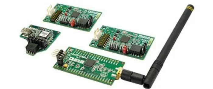
RayMing PCB HM-20 cc2340 BLE5.3 Bluetooth Module Transmission Compatible with Multi-point Links
Master-Slave Integration Remote Control Firmware Upgrade Command Rich
Bluetooth Updates
The generation of a new or updated version of Bluetooth means that there was a previous version, which is an improved one. However, the updated version has to be compatible with various peripheral gadgets and be more efficient for it to earn the name “updated version.” BT 5.0 provides all this and more.
However, after upgrading to a gadget that supports BT 5.0, you might not notice the difference if all your BT accessories only support older BT versions. That is because BT tends to be backward compatible. Therefore, it will sync with older BT versions and still function but not to its full power. This is beneficial since you can continue utilizing your accessories even if they only support BT 4.0 until you purchase an updated version. However, when you connect accessories that function with BT 5.0 with your device (that also supports BT 5.0), you will feel the difference immediately.
How much power does BT 5.0 have to offer?

Compared to the previous version (BT 4.2), Bluetooth 5.0 is more powerful, and it offers improved features such as:
- Lower energy consumption
- It is faster (doubles the speed of 4.2)
- Its range is four times that of its predecessor
- And finally, it can efficiently transfer up to 8 times more data
To put that in hard statistics, BT 5.0 offers a bandwidth of about 2 Mbps. With this bandwidth, BT 5.0 can offer reliable and fast wireless connections, leading to faster data uploading and firmware updates.
Moreover, due to the new range now hits about 800 feet (240 meters), which is a significant improvement from the previous range, which was only 200 feet. As a result, you can utilize your wireless headphones and speakers from a further distance from the source. However, barriers tend to affect BT signals slightly, but this is an excellent leap in BT technology. Due to this upgrade, you can now connect all intelligent home gadgets, for example, thermostats, smart fridges, and cameras, with much ease.
Moreover, due to how Bluetooth 5.0 is efficient in terms of utilizing channels of broadcasting on the famous 2.0 GHz band, this tech has paved the way for beacon-based, richer connectionless Bluetooth solutions. This means that you should expect more efficient wireless connectivity wherever you go, whether in a shopping center or a sports stadium.
Advanced Features of Bluetooth 5.0
Using Bluetooth 5.0, you can connect multiple headphones or speakers to a single source due to the Dual model update that came with this version. Moreover, if your gadgets bear all the proper functions, you can independently reduce or increase the volume of every headphone or speaker.
Moreover, using Bluetooth 5.0, you can stereo pair two speakers to play music seamlessly, with dedicated right and left channels. Using these features, you experience music like you are in another dimension.
Another feature that sets BT 5.0 apart from other BT versions is that it can detect and prevent interferences from close-by LTE bands. Due to this feature, you get to listen to music clearly with minimal interruptions.
When can you get BT 5.0?
Bluetooth 5.0 is already on the market today. Multiple gadgets, for example, most android smartphones, support Bluetooth 5.0. However, even after purchasing Bluetooth 5.0-enabled smartphones, you will still need BT 5.0-enabled peripheral gadgets. However, these gadgets are not widespread as of 2022, but multiple manufacturers are working on producing these gadgets tirelessly.
For iPhone users, you can gain a better experience through the AirPods, which are Apple’s gadgets. Moreover, you can also choose to go with the beast headphones because they also work seamlessly with BT 5.0 due to the new W1 chip. Additionally, if you decide to go with third-party BT headphones rather than purchase Apple’s own BT gadgets, you can still gain a great experience with your iPhone.
Upgrading Tips
As far as upgrading is concerned, you might find it hard to upgrade all your gadget at once, it is not advisable. However, having Bluetooth 5.0-enabled gadgets, such as a laptop or smartphone, will help you a lot in the long run. That is because after attaining this device, you can purchase other peripherals, for example, a BT-5.0 enabled mouse or keyboard, one by one. Moreover, since Bluetooth is getting more powerful and reliable each day, consistently making your purchases will ensure you get the best out of BT 5.0.
Bluetooth 5.0 Programs
The Bluetooth 5.0 standard is to be implemented in the following programs:
Peripherals
Technicians have found means to integrate BT 5.0 into various peripherals that include:
- Printer
- Headsets
- Mouse
- Keyboards (wireless)
Wireless speakers
Moreover, specialists have found a way to integrate Bluetooth capabilities into car sound programs and wireless speakers. Doing so has aided the advancements of hands-free pairing with mobile phones.
VR and AR
As of the 21st century, VR (Virtual Reality) and AR (Augmented Reality) have become a hit. As a result, most people now want to be immersed in the 3D world. And to make this experience even better, technicians have made BT 5.0 compatible with these two trending technologies.
Health Monitory Gadgets
Health is an essential aspect of the world that we live in, and hence companies are trying to find ways to synchronize tech into health to improve our livelihood. One way that manufacturers have made use of this concept is by the introduction of physical and sports fitness monitoring software and gadgets. Moreover, BT-5.0 tends to be a crucial element in this area. Hence it will be heavily utilized to manufacture these gadgets.
Health Care
Bluetooth 5.0 will also be integrated into the healthcare system. Doing so is predicted to make operations more seamless in many medical facilities.
IoT gadgets
Bluetooth 5.0 is also integrated into IoT gadgets. Due to this integration, and the bandwidth BT 5.0, you can easily monitor and control various smart home gadgets with ease. Moreover, you can also synchronize them.
Advantages of Bluetooth 5.0
Improved Internet of things platforms
Improved connectivity, speed, and other positive features of Bluetooth 5.0 have significantly boosted the IoT industry. In addition, the range factor, to be specific, has taken IoT gadgets to another level.
Omnipresent Connectivity
Bluetooth 5.0 allows for omnipresent connectivity where multiple wireless gadgets can function in a single area. This could have been an issue when using earlier versions due to disruptions from colliding signals, destabilizing connectivity, and subsequently furnishing poor connection.
Improvements in Location-awareness
Every Bluetooth cell tower has a fixed location with known sets of accurate coordinates. Manufacturers take advantage of this BT 5 feature to gain a user’s specific location. They can then utilize this information to offer clients a personalized experience. Moreover, since most people place their BT gadgets close to their phones, they can easily track down their devices using this feature.
The Surge in Advert Packets
The BT pairing action that occurs before you connect two or more gadgets has become more reliable, stable, faster, and stronger with BT 5.0 due to a boost in the number of advert packets. When connecting to a new device, the advert packets ask for the device’s name before connecting to it, and therefore it boosts the tech’s reliability quotient.
Disadvantages of Bluetooth 5.0
Even though BT 5.0 is pretty efficient in terms of operations, it still has some cons that you should consider before integrating it into your system.
Power Consumption
Though, on average, BT 5.0 consume less power than its predecessor, that does not eliminate the fact that it still drains your battery. When you enable Bluetooth on your gadget, it scans for BT signals continually, looking for devices to connect. During this scanning period, Bluetooth uses up a lot of energy, automatically draining your smartphone battery.
Weak Security
Compared to Wireless Fidelity (Wi-Fi) and other more advanced wireless data transmission standards, Bluetooth has weak security. And considering that Bluetooth is used in IoT gadgets such as security cameras and hospital management systems, this is a crucial disadvantage.
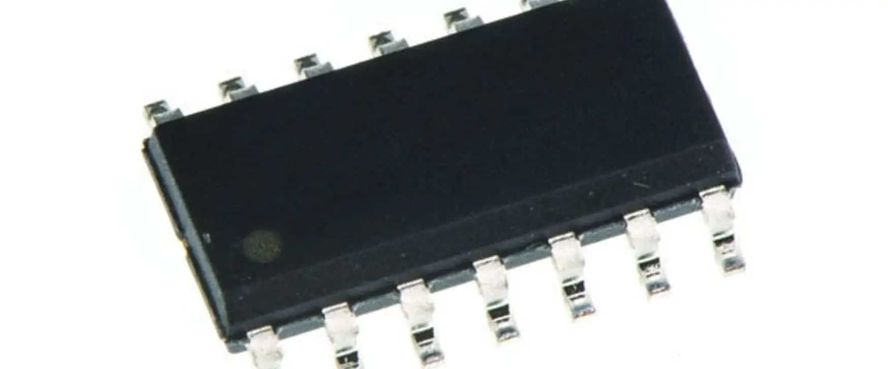
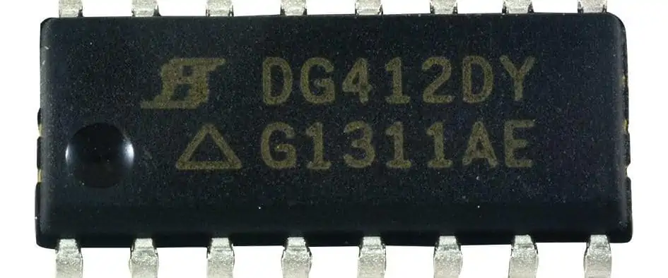
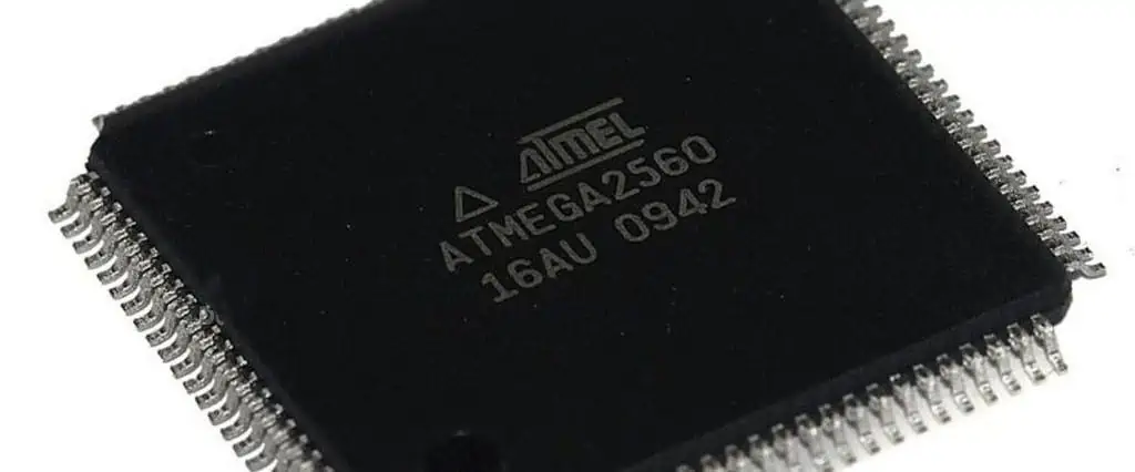
BT 5.0 Control Board
Though BT 5.0 is efficient, it must come with a corresponding BT 5.0-enabled PCB to function.
What is a Control Board?
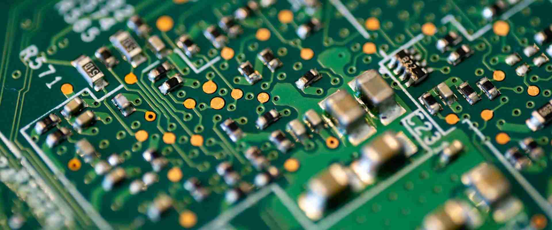
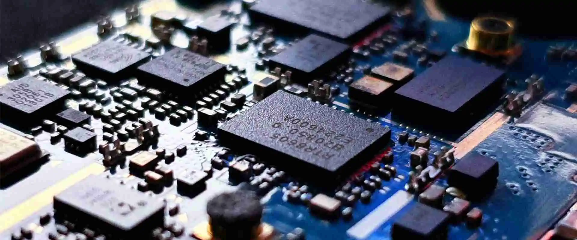
A control board or a Printed Circuit Board is an electronic gadget that utilizes copper conductors or tracks to generate electrical connections between various electrical components. PCBs provide sufficient mechanical and electrical support to various electrical components, which helps technicians mount devices in enclosed tiny areas.
A PCB board design must align with specific manufacturing guidelines to produce a functional PCB. Moreover, the design has to integrate circuit packaging and the bared board’s structure.
Conductive features that you can find on a PCB include:
- Conductive planes
- Pads
- Copper traces
Moreover, the board’s mechanical structure tends to encompass insulating elements laminated between conductor layers. At the end stages of the manufacturing process of a PCB, the board’s structure is platted and then it is covered using solder mask (non-conductive). To top off the board’s design and create a place to write content onto the board, the manufacturer then adds a silk screen as the top layer of the board.
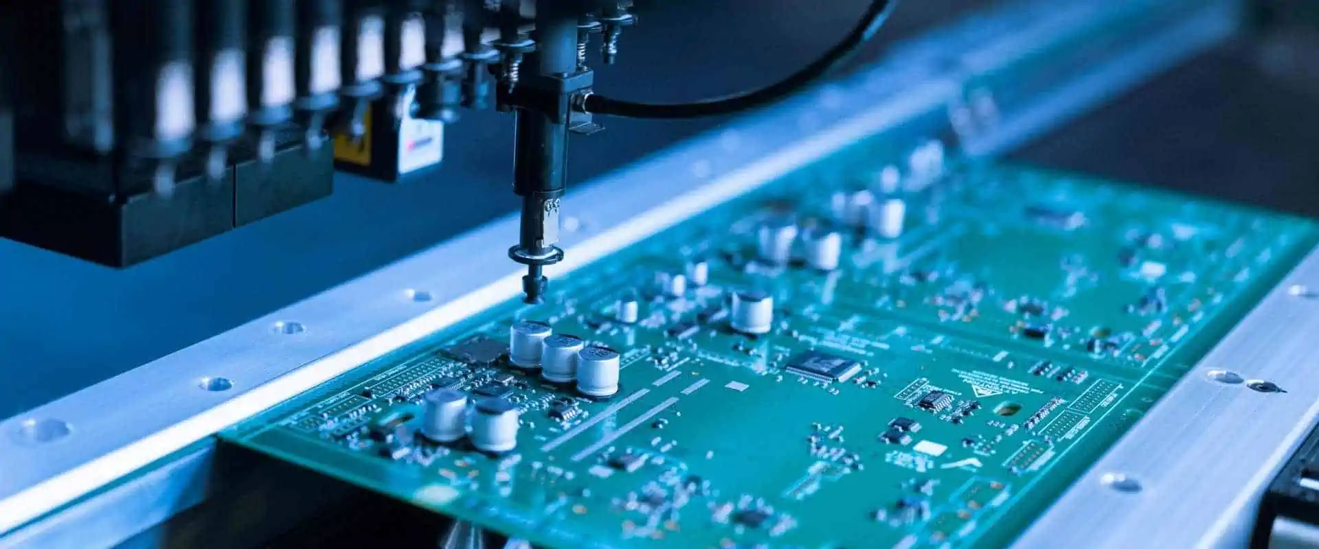
To generate a PCB, manufacturers pass a copper plate through a process known as fabrication. During this process, technicians undertake the following steps to create a PCB:
Laser imaging
Before technicians work on the PCB, they have to mark the areas that will eventually become the metal ground, pads, and traces of the board on the copper plate. To do so, they utilize a mechanism known as laser imaging.
Etching
Etching involves removing excess or unwanted copper from the inner layer of the copper plate. Doing so reveals pads and traces on the copper plate, and now the board starts to look like a Printed Circuit Board.
Layer Stacking
The following fabrication process involves stacking various PCB layers according to the design and then laminating them via pressing and heating. At this point, manufacturers separate the PCB fabrication process for PCB according to how many layers they have since a board with more layers requires more attention.
Drilling
At this stage, technicians utilize specialized equipment and computer programs to drill tiny holes (VIAs) onto the board. These holes are crucial since they are the holes that technicians use to mount various components onto the board.
Plating

The next phase of the fabrication process involves platting the vias and pin holes of the PCB. Doing so makes the PCB more efficient.
Protective Coating
The technicians add a protective coating to the solder masking or surface finish at this stage. Doing so protects the PCB against external contaminants. Moreover, it makes the board more durable.
Silkscreen Printing
Silkscreen Printing involves adding a silkscreen layer onto the control board and then using this layer to add writing to the board. Inscriptions that you can find on this layer include:
- Logos
- Polarity indicators
- The board serial number
- Manufacturing Company
Surface Finish (optional)
In some cases, technicians might decide to add a finish to the copper areas. Doing so will boost the durability of the control board but at a cost.
And that is the control board manufacturing process.
However, although this process seems simple, it gets complex when you add new variables, such as the Bluetooth 5.0 variable. Therefore, most manufacturers are struggling to adjust to this new technology. However, some companies are already there, ready to make your project a reality. These companies include Rayming, a PCB manufacturing company that has been in the industry for a couple of years.
Rayming Support to the Bluetooth 5.0 PCB industry
Rayming is a Chinese PCB manufacturing company that provides complete Printed Circuit Board assembly services. Moreover, the company has been in the industry for over 15 years. Therefore, it has a lot of experience when it comes to PCB assembly.
Rayming provides the latest control board manufacturing technologies, which helps them major in complex areas such as the production of BT 5.0-enabled circuit boards. Moreover, their cutting-edge technology helps them develop high-quality PCBs at affordable prices.
Rayming BT PCBs
BT PCBs produced by Rayming provide highly economical, low-power consumption BT radio that you can utilize to add wireless capabilities to your gadget. Moreover, the on-BT Printed Circuit Board module supports multi-interface protocols; hence it is pretty easy to use.
Through years of experience, Rayming has developed a way to carefully design BT PCBs to cater to your needs. Moreover, they have found means to add a new feature that allows you to connect a USB-UART board to your PCB and control it via your personal computer as a standalone BT device without having to utilize a microcontroller.
Through these advances, Rayming has supported the BT industry tremendously. But moreover, their support does not end at that point.
How to generate Bluetooth Control Boards Rayming Style
Generating a new BT product or any wireless gadget can be a great hassle to many people, especially the inexperienced. The reason behind this is mainly because of the effort that has to go into developing a Printed Circuit Board layout that can support radio frequency transmission. Therefore, if you nail this section, you are probably good at generating a BT 5.0-enabled PCB. Fortunately, when working with a BLE microchip, you will find that most circuitry related to RF is internal. Therefore, when working with this microchip, all you have to worry about is the antenna layout.
Using this tactic, you can quickly produce your BT-enabled PCB board at home. However, for optimum results, you can still create the board using Rayming.
Control Board Manufacturing Services that you can find in Rayming
If you seek to produce your Bluetooth PCB via Rayming, then here are the services that you will enjoy:
- Turnkey PCB assembly services
- Partial turnkey PCB assembly services
For Turnkey PCB assembly, Rayming handles the entire PCB assembly process, which includes manufacturing the circuit board, procuring materials and components, PCB assembly testing, final assembly, and continuous board monitoring for quality assessment purposes.
On the other hand, for the partial turnkey assembly service, the customer provides specific components to the company, and then Raymond handles the remaining production process.
Certifications and Qualifications
Other than being pretty versed in the control board manufacturing industry and having the ability to produce BT-enabled PCBs, Rayming has the following certifications:
- The company is ISO9001 – certified
- Moreover, it is also IPC-A-610 and IPC-A-600 compliant
Therefore, they make quality products each time.
Moreover, the organization has a well-developed printed circuit board manufacturing facility; hence it can process orders pretty fast. Moreover, Rayming has an entire team dedicated to procurements. Therefore, you can be sure that they will utilize the highest quality products in the market to produce your PCB.
Rayming has its headquarters in Shenzhen, China. However, it caters to orders from various countries, which include Canada, the USA, and so much more.
Therefore, if you have a project that requires a BT-5.0-enabled PCB, then Rayming PCB might help you out.
Conclusion
The Bluetooth standard has become a crucial element in the electronics industry. Almost every gadget you come into contact with bears Bluetooth functionalities ranging from fridges, cameras, smartphones, etc. Moreover, over time people have become fond of the wireless world, where you do not need earphones or headphones with cables. Most smartphone companies have eliminated the jack port people use to connect earphones to smartphones and left users to use Bluetooth as the only audio-out option. With this trend in the industry, you can predict that BTs will grow even more in popularity over time. Hence learning how to incorporate them into your project should help you take your device to another level. Moreover, learning about the manufacturer that can help you produce BT 5.0-enabled PCBs should save you a lot of