Why Arduino ATmega 32u4 is a Highly Preferred Microcontroller Board?

Arduino ATmega 32u4

The Arduino ATmega32u4 comes with a lot of features. This makes it a widely integrated microcontroller board in several applications. Read further to learn more about Arduino ATmega32u4 and what it offers.

 What is Arduino ATmega32u4?

The Arduino ATmega 32u4 is a family of 8-bit microcontrollers. It shares some similarities with the ATmega328P. However, the Arduino ATmega32u4 internally handles USB communication. The 328P doesnโ€™t communicate with a USB cable. Therefore, boards that integrate 328P requires a USB-to-serial converter to program.

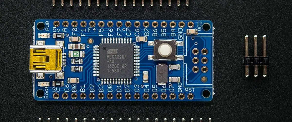
The ATMega32u4 is an 8-bit AVRs that comes with a flash memory of 32kB. Also, it has timers, ADCs, and UARTs among others. One of the benefits of using the Arduino ATmega 32u4 is its low cost. This board is much cheaper than ATmega 328 boards. Also, ATmega 32u4 can execute regular things other Arduino boards canโ€™t. One of these things is the ability to copy a USB mouse or keyboard.

Despite the numerous benefits of ATmega 32u4, this board has its own drawbacks too. It can be more difficult to utilize and can be less reliable. Furthermore, ATmega 32u4 comes with a built-in USB communication. With this feature, there is no need for a secondary processor. There are several microcontroller boards based on the ATmega 32u4. An example of such microcontroller board is the Micro.  

The Micro board works in a similar way with the Arduino Leonardo. This similarity in their operation and functioning is due to the integration of ATmega 32u4.

Since Arduino ATmega 32u4 controls its USB connection, this makes it a more flexible option compared to 328P boards. The ATmega 32u4 can be easily programmed to function as a mouse, MIDI controller, or a keyboard when connected to a computer. These capabilities arenโ€™t possible with 328P boards.

ATmega 32u4 offers support to SPI and 12C communication. Also, this microcontroller board enables CDC communication over the universal serial bus (USB).

Features of Arduino ATmega 32u4

ATmega 32u4

ATmega 32u4 is based on the AVR enhanced RISC architecture. It is a CMOS 8-bit microcontroller. This device provides throughputs of 1 about MIPS per MHz by carrying out strong instructions, enabling the optimization of power. More features of ATmega 32u4 are mentioned below:

High performance

ATmega 32u4 is a high performance and low power 8-bit microcontroller.

Enhanced RISC architecture

The RISC architecture is improved. It includes 135 instructions with single clock cycle execution. Also, it is a fully static operation with 32 x 8 general purpose working registers. This architecture is about MIPS throughput at 16MHz.

Non-volatile program and data memories

ATmega 32u4 features non-volatile data memories and program as it comes with

  • 6/32KB of In-System Self-Programmable Flash
  • 1.25/2.5KB Internal  SRAM
  • 512Bytes/1KB Internal EEPROM

I/O packages

The I/O packages comprise 26 programmable input/output lines, 44 lead QFN package, 44 lead TQFP package and I/O combine LVTTL inputs and CMOS outputs.

Special microcontroller features

ATmega 32u4 comes with an internal calibrated oscillator, programmable brown-out detection, external & internal interrupt sources, and Power-on Reset. Also, it comes with six different sleep modes which are Power-down, Extended Standby, ADC Noise Reduction, Power-save, Standby, and Idle.

IEEEยฎ std. 1149.1 compliant JTAG interface

The JTAG interface has boundary-scan capabilities based on the JTAG standard. Also, this interface allows programming of EEPROM, Lock Bits, and Flash.

Other Features of Arduino ATmega32u4

FULL PCB MANUFACTURING Quote
  • Strictly complies with Universal Serial Bus Specification Rev. 2.0
  • It offers supports to data transfer rates of about 1.5 Mbit/s  and 12 Mbit/s
  • ATmega has six different programmable Endpoints that comes wit In or Out Directions and with Bulk, Interrupt or Isochronous Transfers
  • Features 48 MHz from PLL to enable Full-Speed Bus Operation
  • The size of configurable Endpoints of this microcontroller size is about 256 bytes in double bank mode
  • Fully independent 832 bytes USB DPRAM for endpoint memory allocation
  • Comes with suspend/Resume Interrupts
  • Offers crystal-less operation to enable Low-Speed mode
  • It is possible to execute CPU Reset on USB Bus Reset detection
  • It is equipped with USB Bus Connection/Disconnection on Microcontroller Request

Peripheral Features of Arduino ATmega 32u4

  • Four PWM Channels that has Programmable Resolution ranging from 2 to 16 Bits
  • On-chip Temperature Sensor
  • One 10-bit High-Speed Timer/Counter with PLL (64MHz) and Compare Mode
  • Four 8-bit PWM  Channels
  • Six PWM Channels for High-Speed Operation, with Programmable Resolution from 2 to 11 Bits
  • On-chip PLL for USB and High-Speed Timer : 32 up to 96MHz operation
  • Byte-Oriented 2-wire Serial Interface
  • Output Compare Modulator
  • Two 16-bit Timer/Counter with Separate Prescaler, Compare- and Capture Mode
  • One 8-bit Timer/Counter with Separate  Prescaler  and Compare Mode
  • Programmable Serial USART with Hardware Flow Control
  • 12-channels, 10-bit ADC (features Differential Channels with  Programmable Gain )
  • Master/Slave SPI Serial Interface
  • Programmable Watchdog  Timer with Separate On-chip Oscillator
  • Interrupt and Wake-up on Pin Change
  • On-chip Analog Comparator

Applications of ATmega 32u4

ATmega 32u4 is a low power microcontroller ideal for many applications. Some consumer electronics feature this microcontroller board.

  • Automation and control process
  • Sensors and instrumentation
  • Consumer electronics
  • Appliances
  • Circuitry to control processes
  • Monitoring medical equipment
  • Rectification
  • Motor control
  • DAC applications
  • Power regulation

Boards Based on the ATmega32u4 Microcontroller

There are several boards based on ATmega32u4 microcontroller. Examples of such boards are the Arduino Leonardo board and The Micro.

Arduino Leonardo board

This board operates based on ATmega32u4. It features a power jack, a micro USB connection, 20 I/O pins, and in-circuit serial programming. The Leonardo works in a different way from other Arduino boards. This is because of its inbuilt USB 2.0 communication.

Arduino Leonardo board integrates a single microcontroller to communicate with your personal computer. This makes Leonardo a more flexible option for communicating with a computer.
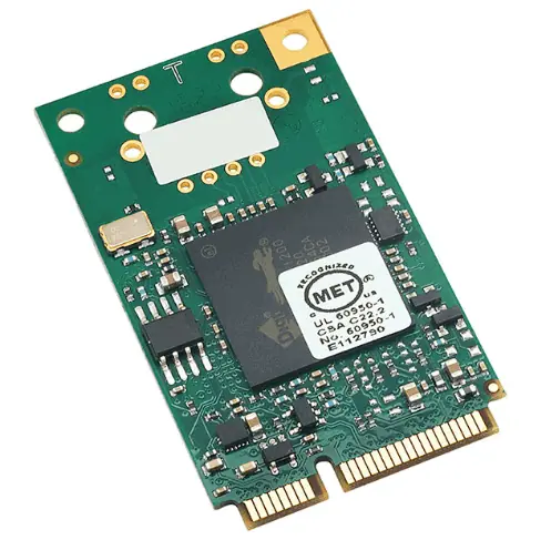
The Micro

This microcontroller board is also based on ATmega32u4. The Micro has an ICSP header, a reset button, a 16 MHz crystal oscillator, and 20 digital I/O pins. This board shares some similarities with Arduino Leonardo due to the built-in USB communication of ATmega32u4. With this, the Micro appears to a computer as a keyboard or a mouse.

The ATmega32u4 integrated in this board is already preprogrammed using a bootloader. This enables users to upload new code without the need for an external hardware programming. Also, users can ignore the bootloader and use the ICSP header to program the microcontroller. You can use a USB connection to power the Micro.

What is the Difference Between Arduino ATmega32u4 and ATmega328P?

The ATmega32u4 and ATmega328P both belong to the AVR family. These two microcontroller boards share some similarities. However, they have some differences. One of the differences is that the ATmega32U4 features a USB device peripheral while the 328P doesnโ€™t.

Furthermore, ATmega32u4 is more expensive than the ATmega328P. The ATmega32u$ offers support to serial while ATmega32u4 only works with USB. If you need a keyboard, the ATmega32u4 is a great option. However, there are some applications that require the use of serial.

For programming, the ATmega328P requires a USB-to-serial converter. This is because this microcontroller board doesnโ€™t communicate with a USB cable. The biggest benefit of ATmega32u4 is the built-in USB which enables it function like a USB keyboard, MIDI or a mouse. Also, ATmega32u4 is widely integrated in Aduino Leonardo and other compatible boards.

Frequently Asked Questions

How can a bootloader be written for ATMEGA32U4?

The built-in USB interface of Arduino ATmega 32u4 is one of its great features. This feature makes it very easy to program. All you just need to do is to connect a USB cable and voila! The Arduino bootloader will need to be burnt to the Arduino sketches to help upload the sketches. You can make use of the Arduino Uno if there is no programmer.

How can a keyboard be connected to the ATMEGA32U4?

The Human Interface Device (HID)is one of the defined USB device classes. Each USB device has a device class. The device class specifies the general purpose of the USB device. There are a wide variety of classes which include speakers, hubs, webcams, and printers among others.

Which microcontroller board is based on ATMEGA32U4?

The Micro is a microcontroller board that integrates the ATmega32u4. It comes with 20 digital I/O pins, a reset button, a 16 MHz crystal oscillator, an ICSP header, and a micro USB connection. The Micro features every important element required to support the microcontroller. All you need to do is to connect the Micro to a computer using a micro USB cable.

How can I recognize the ATmega32U4 via USB?

The ATmeaga32u4 allows the connection of USB pins to a special hardware to perform USB signaling. The hardware pretty supports the electronics, but, it doesn’t control the received or sent data. Also, you need to send and receive the data to identify the device. If the chip has no software, it wonโ€™t send any data. Windows will most likely reveal that one of the connected USB devices has malfunctioned. However, it might not be able to detect it.

Conclusion

Since the Arduino ATmega 32u4 controls its USB connection, this makes it a more flexible option compared to 328P boards. The ATmega 32u4 can be easily programmed to function as a mouse, MIDI controller, or a keyboard when connected to a computer. These capabilities arenโ€™t possible with 328P boards.

Top 9 Applications of Home automation using IoT

IoT Devices

IoT home automation involves utilizing internet-connected devices to control various household appliances. It can include setting up intricate heating & lighting systems and managing home security controls and alarms, all of which are linked to the central hub and can be operated remotely using the smartphone app.

Despite the prevalence of mood-sensing music systems, motorized blinds, intelligent heating & cooling, bright lighting, and automated doors and windows in the constantly connected world of IoT home, there seems to be a lack of dialogue about why consumers have not fully embraced the hype around IoT home or whether it has genuinely enhanced domestic life.

The American Association of Home Builders coined the term “smart house” in 1984. However, IoT smart homes, or home automation using IoT, gained popularity in the 2000s. 

With the advent of several affordable, intelligent technologies, smart houses became a viable option for consumers. The Echo IV, introduced in 1966, was the 1st IoT home automation system.

It lets customers make grocery lists, adjust their house’s temperature, and turn appliances on and off. The kitchen computer, created in the 1960s and developed recipes, was never a commercial success due to its high price.

In an IoT smart home, a central hub connected to the internet manages all the individual devices. The hub is then regulated using a smartphone application. The setup process for an IoT smart home can be complicated as specific add-ons are compatible with particular devices.

Internet-connected home security features like alarm systems and access control are also part of the equation. Once domestic appliances are linked to the internet, they become a significant aspect of the Internet of Things.

Home automation systems typically link controlled devices to a central hub/gateway. The control program for the system can be accessed through a tablet, wall-mounted terminals/desktop computers, phone applications, or an online interface that can be accessed on the internet from a remote location.

Home automation using IoT for Smart Home

IoT technology is poised to permeate nearly every facet of our daily lives, enhancing our comfort and security. According to Statista, there will be an estimated 30.9 billion IoT connections by 2025. In this article, we will examine the most prevalent methods for utilizing IoT technology in intelligent houses. 

Smart IoT sensors are aware of our temperature, music, and lighting preferences, as well as our daily routines, such as waking up, eating, and going to bed. Smart plugs, lights, & security systems work together to simplify our lives. With just a smartphone application, we can easily control our house security even when we’re not there.

Applications of Home automation using IoTSmart Homes

1. Lighting

The lighting in a home can now be adjustable to cater to individual needs. For instance, if people start watching a movie, the lights can be programmed to dim automatically to prevent any disruption to the viewing experience. Similarly, when you enter your house, the lights can switch automatically without requiring you to press a button.

The system can automatically reduce the lights when you leave your house to conserve energy, eliminating the need for you to do so manually. You can use your laptop, smartphone, and other connected devices to control all of the lights in your home. This allows you to schedule your app to turn on the lights when the alarm goes off. 

2. Bathrooms

IoT technology can enhance the convenience and enjoyment of your everyday routine in the bathroom. Intelligent mirrors can connect to other appliances like computers & smartphones, recognize the faces of members standing near them, and display personalized information such as weather forecasts, news articles, and specific websites that interest each individual. 

Special sensors can detect movement and automatically switch off the water in the bathroom if no one is present. Smart shower controls can also recognize individuals and adjust the water temperature and pressure to their preferred settings while limiting the time spent in the shower to conserve water. 

Automated jacuzzi users can relax and enjoy the bath without manually adjusting the temperature, air-jet regime, or music preferences, as the app manages everything for them

3. Gardens

Sensors can be helpful for individuals who desire to grow their vegetables, fruits, and herbs in the house. Users can use the app to check whether the optimal temperature and the plant are adequately hydrated.

The software can monitor the soil’s current condition, check if it has enough moisture, and activate an irrigation system if necessary. 

IoT technology has brought significant advancement in gardening, revolutionizing the way plants are grown. Sensors can detect the ideal moisture level and turn off the watering system, preventing water waste. The software can track the soil’s current status, determine if it has adequate moisture, and activate an intelligent irrigation system if needed.

4. Kitchen

FULL PCB MANUFACTURING Quote

By utilizing AI technologies, IoT devices can make cooking easier and safer. Smart sensors can also monitor smoke & carbon monoxide, as well as the temperature & humidity levels in the kitchen. 

IoT devices incorporating AI technology can make cooking safer and more accessible. Intelligent sensors can monitor the kitchen for smoke, carbon monoxide, and temperature and humidity levels to ensure everything is in working order. Built-in applications can track food availability in your fridge, give recipe suggestions, and reach the nutritional value of meals. Additionally, intelligent spoons can encourage users to eat slowly.

5. Security Systems

Do you consistently verify whether the doors & windows are closed, and the computer, TV, and other electrical devices are switched off before departing your residence? Utilizing specialized sensors, intelligent security systems can perform this task on your behalf.

As you depart from your home, these controllers can lock the entryway, shut the window covers, power down electronic appliances, protection against any human/animal intruders. Using the app on mobile devices, users can remotely monitor their homes and control the temperature, humidity, & lighting. In addition, they can keep a watchful eye on their elderly relatives and assist if required.

6. Safety Sensors

Intelligent safety devices equipped with sensors can identify potential hazards in your home and promptly notify you of any issues. These devices can also take preventative measures to mitigate risks. All that is required to utilize these safety features is a phone with internet access and the installation of the sensors within the household.

Temperature, humidity, or gas controls may regularly check the air in your home and notify you through email if anything is outside the recommended range. 

Safety sensors can prevent fires, explosions, water leaks, and gas leaks. Proximity or video sensors can detect attempted break-ins and immediately activate the alarm or notify the authorities.

7. Temperature Control

With temperature control automation, you can adjust the temperature in your home to a level that is most comfortable for you. Users can program smart thermostats to control the temperature based on their preferences and settings, and they can even recognize your current activity and adjust the temperature accordingly.

For example, users can use the app to automatically raise the temperature in their bath or shower or lower it to help them stay calm during at-home exercises like yoga, pilates, or other physical activities.

8. Doors and Windows

embedded iot

In the future, keys will no longer be necessary for our doors. Doors may utilize facial recognition technology to unlock your house, and anyone entering who is not recognized as a resident will need to be identified. You could even program the doors to open as you approach your home and close as you leave.

Opening a door could trigger a chain reaction in other home appliances, leading to the opening of other doors when authorized users are detected, or the automatic turning on of the TV or coffee maker.

Bright windows can be programmed to respond to various events and signals from other devices. With such a system, the windows can automatically detect and close themselves when necessary, eliminating the need for you to worry about losing them when leaving the house.

9. Home Routine

By utilizing AI and ML technologies, you can manage your home’s temperature, lighting, and security system. The technology can notify you of necessary purchases through an online app, search for information online, provide news updates, order meals, schedule appointments, and even book lodging or travel arrangements.

You can monitor the status of your home automation from anywhere. By using the app, you can verify the functionality of your lighting, security, and other internet-connected devices while you are out and about, visiting your parents or friends.

Sensors for Home automation using IoT

IoT sensors have the potential to significantly elevate our quality of life while also improving home security. Intelligent motion controllers can detect the presence of someone on your property and, through the app, alert users of any intruders, whether human or animal.

Smart controllers within the network ensure that all windows and doors are closed when residents depart the house at night, as well as during certain weather conditions, such as rain or storms.

Using the controls at your disposal, you may adjust the lighting, humidity, and temperature. Smoke controllers help prevent house fires, whereas carbon monoxide detectors help to prevent carbon monoxide poisoning.

Understanding the key fundamentals of Imagineering PCB

imagineering PCB

Imagineering PCB is a term that describes creating custom-designed printed circuit boards (PCBs). PCBs should adhere to strict specifications by combining engineering with imaginative thinking.

We can design the circuit board using sophisticated software tools and produce the actual circuit board via manufacturing. In addition to designing unique circuits not commonly available in commercially available PCBs, Imagineering PCB may also entail this.

Imagineering PCB companies can offer various services, such as design, layout, prototype, and manufacture. Also, they could collaborate with clients to create unique PCBs that address certain issues or demands.

The benefits of Imagineering PCB

Imagineering PCB is a potent tool that combines engineering and imagination to produce specially designed printed circuit boards (PCBs) that adhere to certain specifications. As a result, Imagineering PCB has various advantages, from increased performance and usefulness to more customization and flexibility. We’ll look at some of the significant benefits of Imagineering PCB in this article and how they promote innovation and development in electronics manufacturing.

Custom circuits

Imagineering PCB’s capacity to design bespoke circuits that are not commonly available in off-the-shelf PCBs is one of its main advantages. With the aid of Imagineering PCB, designers and engineers can produce one-of-a-kind, cutting-edge circuits suited to particular applications, enhancing performance and functionality. Imagineering PCB may minimize power consumption, boost processing speed, and enhance signal integrity, among other advantages, by developing bespoke circuits. This customization may be beneficial in sectors like aerospace, medical technology, and industrial automation, where ordinary PCBs might not be able to satisfy unique needs.

Unique designs

The capacity to produce original and cutting-edge designs that can aid in differentiating items in the marketplace is another advantage of Imagineering PCB. We can make products that stand out from the competition. They can provide a better user experience with the aid of Imagineering PCB. This is particularly relevant in consumer electronics, where product success depends on design and aesthetics. Designers may produce goods that are not only useful but also aesthetically pleasing and engaging by employing Imagineering PCB.

Flexibility and adaptability

Moreover, Imagineering PCB provides more adaptability and flexibility during the design process. Imagineering PCB enables simple customization and circuit design change, unlike off-the-shelf PCBs, which are made for specific purposes and cannot be readily modified. This flexibility may be beneficial as design changes, and iterations are frequent in product development. With the aid of Imagineering PCB, designers can rapidly alter circuit designs to satisfy shifting specifications, hastening the creation of new products and their time to market.

Efficiency

The capacity to lower costs and increase production efficiency is another advantage of Imagineering PCB. Imagineering PCB may assist in lowering component counts, minimizing waste, and raising production yields by developing unique circuits tailored for specific applications. As a result, Imagineering PCB can be a cost-effective alternative for many applications due to lower prices and increased manufacturing volumes.

Innovation

With these advantages, Imagineering PCB is advancing various sectors via innovation. Imagineering PCB, for instance, is being utilized to create cutting-edge virtual and augmented reality technologies, which call for high-performance and unique circuit designs. Furthermore, advanced medical gadgets like implanted sensors and remote monitoring and diagnostics tools are products of Imagineering PCB. In addition, Imagineering PCB is used in the aerospace industry to design compact, high-performance circuits for satellites, spaceships, and other types of spacecraft.

What skills are necessary for Imagineering PCB?

FULL PCB MANUFACTURING Quote

A mix of technical expertise and original thought is necessary for the complicated, diverse area of Imagineering PCB. The engineers and designers who work in Imagineering PCB need to have a thorough grasp of electronics, PCB design, and manufacturing procedures, as well as creative thinking and idea generation skills. The following are some of the particular abilities necessary for PCB imaging:

Electronics Design:

An in-depth knowledge of electronics design, including digital and analog circuit design, signal processing, and power management, is required of engineers and designers working in Imagineering PCB. In addition, they need skills in drawing and analyzing schematics and designing circuit boards. They must adhere to strict specifications and troubleshoot problems while designing.

PCB Design:

An understanding of PCB design, including an understanding of PCB layout, component placement, and routing, is also necessary for Imagineering PCB. Designers must create digital circuit board designs using software tools. It ensures that the layout is optimum for the particular application and that they can produce the board quickly and accurately.

Manufacturing Processes:

Understanding manufacturing procedures are also necessary for Imagineering PCB. The materials used in PCB fabrication and the tolerances and specifications for various manufacturing methods must be all friendly to engineers and designers.

Creativity:

Imagineering PCB demands both technical expertise and creative and original thought. Engineers and designers must think creatively and develop fresh approaches to solving challenging issues. They also need to push the limits of what is practical in electrical design.

Communication and Collaboration:

Working with a group of engineers, designers, and other stakeholders is a common part of the collaborative process known as Imagineering PCB. As a result, effective communication and teamwork abilities are crucial for success in this industry. Engineers and designers need to collaborate with others and be receptive to criticism and suggestions from their peers.

What industries use Imagineering PCB?

Printed circuit boards that are specially to satisfy specific needs are helpful in various sectors. These are a few examples of industries that often employ Imagineering PCB:

Aerospace:

The aerospace sector needs Circuit boards that survive severe temperatures and harsh conditions. Imagineering PCB designs and produces custom PCBs for aerospace applications, such as satellites, spacecraft, and avionics systems.

Medical Devices:

Custom PCBs created to fulfill particular specifications for size, power consumption, and signal processing are frequently necessary for medical devices. Custom circuits for various medical devices, such as pacemakers, implantable devices, and diagnostic equipment, are made using Imagineering PCB.

Industrial Automation:

Custom-designed PCBs are essential for managing and controlling robots, automated manufacturing, and other automated systems in the industrial automation sector. PCBs tailored for certain industrial uses, such as high-temperature conditions, vibration, and shock resistance, are designed and produced using Imagineering PCB.

Consumer Electronics:

Companies that make consumer electronics employ Imagineering PCB to build circuit boards specifically for smartphones, tablets, wearables, and other gadgets. By enhancing performance, these bespoke PCBs enable manufacturers to distinguish their goods in a fiercely competitive market.

Automotive:

For usage in bespoke PCBs for car electronics, including safety systems, infotainment systems, and powertrain control systems, the automotive industry employs Imagineering PCB. These customized PCBs must endure extremely high temperatures and severe conditions and adhere to strict size and power specifications.

Summary

Imagineering PCB is a significant component of contemporary electronics design and production.

The Imagineering PCB is essential for innovation and advancement in electronics design and production. Imagineering PCB enables designers and engineers to build unique circuits that adhere to strict specifications. It results in increased performance, functionality, and design. As a result, Imagineering PCB is advancing technology and enhancing the goods and experiences.

Imagineering PCB calls for a special mix of technical and artistic abilities and the capacity for teamwork and good communication. These abilities enable engineers and designers to produce bespoke circuit boards that adhere to detailed specifications and promote innovation in electronic manufacturing.

Last, Imagineering PCB is helpful in various sectors where specialized printed circuit boards are necessary to satisfy demands. These demands include performance, size, power consumption, and environmental considerations.

How to Design Your Own Custom Microcontroller Unit – MCU PCB

MCU PCB

What is an MCU PCB?

A microcontroller unit (MCU) serves as the main processing unit on an MCU PCB, also known as a microcontroller unit printed circuit board. An MCU is a tiny computer with a CPU core, memory, and input/output peripherals on a single chip. The MCU offers system intelligence and control, enabling it to carry out various activities, from straightforward control operations to intricate computations and data processing.

An MCU PCB generally incorporates extra parts including sensors, actuators, communication interfaces, and power management circuits to support the MCU’s capabilities. To provide the necessary electrical connections, these components are placed on the PCB in a specified layout and connected by traces and vias.

MCU PCBs are ideal for various applications, such as consumer electronics, automotive systems, industrial control systems, and medical devices. They are highly appealing because of their adaptability, affordability, and simplicity. Additionally, their capacity to accommodate a variety of peripherals and interfaces is essential.

Microcontrollers, digital and analog circuitry, programming languages, and PCB layout and design are all specialist skills needed while designing an MCU PCB. To assist their clients in creating custom PCBs that fit their unique specifications, many PCB manufacturers provide design services for MCU PCBs.

How do Microcontroller Units Work PCB

MCU Board

Microcontroller Units (MCUs) are integrated circuits that combine memory, input/output peripherals, and communication interface capability with the computational capacity of a central processor unit (CPU) on a single chip. MCUs are designed to carry out particular tasks and do these tasks by carrying out instructions in a predetermined order.

Several programming languages, including C, C++, and assembly language, can be used to create MCUs. We usually program the MCU using a programming device once we create the code on a computer. The MCU executes the instructions in the order the programmer specified once you load the code.

Memory, another component of the MCU, houses the instructions it carries out. The memory may be either non-volatile. As a result, the data remains even when the power is off. On the other hand, when volatile, we lose the data when the power is off.

An MCU’s input/output peripherals enable communication with other electronics or sensors. The features of the peripherals, which can be analog or digital, include pulse-width modulators, timers, analog-to-digital converters, and serial communication interfaces like SPI, I2C, and UART.

The MCU can use input from peripheral devices to conduct computations or other tasks. The output peripherals, such as a motor controller, LED driver, or display, can output the results.

The MCU collaborates with other components on a PCB to carry out the required task. To ensure that the MCU runs appropriately, the PCB designer must consider the power needs, communication interfaces, and other considerations when creating the PCB layout.

System/Preliminary Design

An MCU PCB’s system or preliminary design specifies the system’s general architecture, its functional requirements, component choices, and high-level design considerations.

Determining the system’s functional requirements is the first step in the system design process. This entails determining the system’s inputs and outputs, the needed processing power, and any other constraints the system must satisfy. A system specification document, employed to direct the design process, frequently includes descriptions of the functional requirements.

The next stage is to select the system’s components after establishing the functional requirements. This entails choosing the microcontroller and any additional parts, such as sensors, actuators, communication interfaces, and power management circuits, which may be needed.

While choosing components, it’s necessary to consider the microcontroller’s compatibility, the system’s power needs, and the intended communication interfaces. Along with performance criteria, availability and the cost is also necessary while choosing components.

We can establish the high-level design of the system once we choose the components. This involves figuring out the PCB’s layout, the system’s architecture, and the electrical connections between its many parts. Finally, we depict the system’s components and their relationships in a block diagram, a common form of documentation for high-level designs.

It’s crucial to consider noise, electromagnetic interference (EMI), and power consumption while designing a system. These variables may affect the system’s performance and require additional design aspects or components.

In general, choosing components, defining the high-level architecture and layout of the PCB, and specifying the functional needs of the system are all steps in the system design process for an MCU PCB. The system design guides the PCB’s intricate design and implementation, which entails developing the schematic and organizing the board’s lines and components.

Schematic Circuit Design

FULL PCB MANUFACTURING Quote

An MCU PCB’s schematic circuit design entails visually depicting the circuit’s electrical connections and constituent parts. A schematic capture program is often ideal for this. It enables the designer to position components and create connections between them.

We must choose the microcontroller and any other components utilized in the circuit before creating the schematic circuit design. This entails choosing the right sensors, actuators, communication interfaces, power management circuits, and other parts necessary to fulfill the system’s functional needs.

After choosing them, the components can go into the schematic editor and connect with wires or nets. The schematic should be labeled and organized to read and comprehend.

The electrical properties of the components and how they interact with one another are essential during the schematic design process. This considers required current flows, signal integrity, and noise levels.

A stable power supply for the microcontroller and other components should be ensured by including appropriate power regulation and decoupling circuits in the schematic design. In addition, the schematic design should also contain any essential protective circuits, such as over-voltage or over-current protection.

We can examine and validate the schematic circuit design once finished to ensure it complies with the system’s functional requirements and that there are no mistakes or omissions. This may entail executing simulations or testing to validate the circuit’s performance.

Overall, because it gives a visual representation of the circuit and acts as the foundation for the layout and implementation of the PCB, the schematic circuit design is a crucial phase in the design process for an MCU PCB.

PCB Layout Design

MCU & MPU Modules
MCU & MPU Modules

Making the PCB layout design is the following stage after finishing the schematic circuit design for an MCU PCB. First, the components must be on the board and route the connecting traces.

We choose the physical size and shape of the PCB as the initial stage in the PCB layout design process. The size and location of the components, as well as any mechanical or thermal factors, will determine the PCB’s dimensions and form.

A PCB layout program helps to arrange the components from the schematic circuit design on the board. The components are ideal for optimal signal integrity, power supply, and thermal management. Apart from noisy or high-current components should be located components that are noise-sensitive or need consistent power. Also, heat-generating components must be close to heat sinks or well-ventilated regions.

Routing the traces that connect the components comes after positioning them. We should optimize the routing for signal integrity, power supply, and noise immunity. Onw should route signal traces to reduce cross-talk and interference as much as feasible. Power and ground planes are necessary for reliable power and ground connections.

Adherence to design standards and guidelines during the PCB layout design process is crucial. This covers specifications for component location, clearances, and trace widths.

The finished PCB layout design should go through inspection and validation. It ensures it satisfies the system’s functional requirements and that there are no mistakes or omissions. To check the PCB’s performance can entail executing simulations or testing.

The PCB layout design determines an MCU PCB’s physical implementation. It is a crucial phase in the design process. This is because it may significantly affect the circuit’s performance, reliability, and manufacturing ability.

Gearing Up with the Smart PCB

smart pcb

Circuit boards have come a long way since their invention in the mid-twentieth century. What was once a collection of discrete components soldered together on a flat piece of fiberglass has evolved into a sophisticated and complex system of layers, tracks, and components that power our world. And now, with the advent of smart PCBs, we expect circuit board design to take another giant leap forward.

Smart PCBs consist of more than just conductive lines linking passive parts. On the board, they directly incorporate active components like microprocessors, sensors, and communication interfaces. A wide range of new features is possible due to this integration, including the ability to wirelessly communicate with other devices and monitor and regulate a motor’s performance. In other words, smart PCBs alter how we approach circuit board design.

Applications of Smart PCB

Here are the main applications of smart PCBs:

Smartwatches, smartphones, tablets, and radios

Mobile gadgets like smartphones, smart watches, tablets, and radios all employ smart PCBs because they provide a convenient and effective way to combine several tasks into a small package. They may have Bluetooth, GPS, Wi-Fi, and other sensors built into their design.

Home desktop PCs, laptops, workstations, and satellite navigation

PCBs are a crucial part of most electronic equipment used in offices and homes, including desktop PCs for the home, workstations, laptops, and satellite navigation systems. These gadgets employ smart PCBs with networking capabilities, high-speed data processing, graphics, and video display capabilities.

Bio-imaging

Powering and managing the electronic components of X-ray screens, CT scanners, and ultrasonic scans depend on printed circuit boards (PCBs). Smart PCBs help guarantee the gadgets’ high precision, dependability, and speed.

Other medical applications

Medical gadgets employ PCBs to power and process electronic components that detect and monitor vital signs. These include blood glucose, heart rate, and blood pressure, monitors. Smart PCBs help guarantee the devices’ accuracy, dependability, and patient safety.

Smart textiles

PCBs can be integrated into clothing and bandages to create smart materials to monitor vital signs or deliver drugs. Flexible and stretchable PCBs help ensure that the textiles are comfortable and durable.

Renewable energy

Renewable energy systems employ PCBs in managing and regulating power generation and distribution. These systems include solar power cogeneration equipment and DC-to-AC power inverters. Smart PCBs help ensure the systems are dependable and effective.

Aerospace

The aerospace industry uses accelerometers, pressure sensors, microphones, torque, and force sensors, and others to measure and regulate numerous parameters in airplanes and rockets. Smart PCBs guarantee the accuracy and dependability of the sensors in harsh conditions.

Textile

PCBs can be applicable in clothing and bandages to build smart fabrics that distribute medications or monitor vital signs. The machines utilize flexible and stretchable smart PCBs to ensure strong and sturdy materials.

Benefits of the Smart PCB

FULL PCB MANUFACTURING Quote

Employing the smart PCB in your design rut comes with the following advantages:

  1. Safety and security enhancements: Smart PCBs can enhance the security and safety of electrical equipment. Smart PCBs can assist in defending against cyber threats and guarantee that electronic devices are safe to use by including encryption, authentication, and access control. Additionally, to reduce the possibility of mishaps and malfunctions, we can equip smart PCBs with safety features like fault detection and self-repair.
  2. Cost savings and a quicker time to market: Smart PCBs can aid in cost savings and a faster time to sell electronic gadgets. Smart PCBs reduce the need for extra components and assembly steps by combining multiple functions onto a single board, which expedites production and lowers costs. Additionally, smart PCBs are easy to design and test quickly using computer-aided design (CAD) software, enabling faster prototyping and production.
  3. Functionality and performance gains: Smart PCBs outperform conventional PCBs in terms of functionality and performance. They can combine several functionalities onto a single board, which helps electronic gadgets become smaller and simpler. Smart PCBs can also combine cutting-edge components like wireless connectivity, sensors, and microprocessors to improve the functionality of electrical products.
  4. Enhanced energy efficiency: Smart PCBs can assist in lowering the energy requirements of electrical equipment. Smart PCBs can help extend battery life and reduce the overall energy consumption of electrical gadgets by utilizing cutting-edge components like low-power microprocessors and energy-efficient sensors.
  5. Increased dependability and durability: Compared to conventional PCBs, smart PCBs are more dependable and long-lasting. They employ cutting-edge materials and parts that can endure extreme conditions, temperature swings, and mechanical stress. Moreover, smart PCBs can incorporate flaw detection and self-repair functions to guarantee long-term dependability.

The future of Smart PCBs

Smart PCBs’ applications and potential uses will only grow as the technology underlying them develops further. Smart PCBs will probably continue to shrink and get more compact, allowing for application in more wearable and portable gadgets. They also improve their energy efficiency, allowing for more battery-powered devices.

Future developments could also see smart PCBs grow in wit and autonomy. They may be able to pick up on new information and adjust to different contexts, allowing them to carry out increasingly difficult jobs without assistance from a human. In addition, they may make a new degree of automation and control possible through their potential to interface with other systems and devices in novel ways.

Smart PCBs’ integration with other cutting-edge technologies, including artificial intelligence and the internet of things, is an intriguing future potential (IoT). We can develop fully intelligent and interconnected systems that can sense, evaluate, and react to their environment in real time by fusing the intelligence and connectedness of smart PCBs with the strength of AI and the massive IoT device network.

With this promise comes the need for accountability and caution, though. It’s crucial to consider smart PCBs’ moral and societal ramifications, as with any new technology. How, for instance, can we guarantee that these intelligent systems are safe and secure and won’t endanger people’s security or privacy? How do we ensure that they benefit society as a whole rather than just the interests of a few powerful actors?

With this technology’s continued advancement, we might anticipate seeing brand-new, cutting-edge applications arise in various fields and businesses. We must handle this technology with prudence and responsibility to ensure it benefits society. By doing this, we can make the most of smart PCBs’ possibilities and move forward to a future that is intelligent and affluent for everyone.

Conclusion

No one could have imagined all of the amazing possibilities smart PCBs offer during the early stages of their invention. But we have come a long way, and now with the help of smart PCBs, we can take circuit boards to the next level. Whether it’s powering the latest mobile gadgets or regulating renewable energy systems, the applications of smart PCBs are endless. But, with that, we must continue using them responsibly to ensure a safe and prosperous future for all. So, let’s all be smart and use smart PCBs!

Impact of CPU PCBA in Computing Devices

CPU PCBA

The CPU is the brain of a computing device. It is the electronic circuitry that carries out instructions in a computer. The central processing unit or central processor carries out basic functions like basic arithmetic, controlling, logic, and input/output operations.

A wide range of devices integrate a CPU. Examples of such devices include smartphones, computers, desktop, flat-screen television set, and laptop. Over the years, the CPU has been described with several names like computer processor, processors, and microprocessor. A modern processor is always small in size and has a square shape.

Without a CPU, a computing device will fail to function. The CPU is the brain behind all the operations performed by your smartphone or PC.

What is a CPU PCB?

CPU PCB

The CPU PCB is the main circuit board of a CPU. This board contains the microprocessor and as such plays a very important role in a CPUโ€™s functionality. According to some computer engineers, the CPU PCB is externally connected to the microprocessor. The motherboard of a computer comes with slots for the external storage devices.

The printed circuit board offers electrical connection and mechanical support to electronic components. A CPU PCBA comprises electronic components which are responsible for functioning of the CPU. This circuit board functions as the platform for the central processor of a computing device. A CPU PCBA comprises peripheral component connection and modular PC cards.

The circuit board of a central processor comprises thousands of capacitors, transistors, and resistors. All of these components play a crucial role in the function of the CPU. The CPU is mounted on a circuit board.

Guidelines for CPU PCBA

The CPU PCB assembly is different from conventional PCB assembly in some ways. When assembling a CPU PCB, strict measures need to be taken. Also, a multilayer PCB is often used in a CPU PCBA.  Here are important guidelines to follow during CPU PCB assembly:

Select the type of mounting technology

In PCB assembly, there are two major technologies for mounting components on a bare board. The surface mount technology (SMT) and through hole technology (THT) are commonly used. SMT makes use of an automated process to mount component on a bare board. This mounting technology is very fast as components are placed by using an automated machine.  Through hole technology, on the other hand, requires drilling of holes in the bare board.

USB to serial converter

There is a need for a central processor to interact with the computerized system. This interaction enables them to function as expected. Therefore, an additional chip is required in order to translate the signals from the central processor.

Determine the microcontroller

The microcontroller is the core of a CPU PCB. Therefore, you need to choose the right microcontroller that meets the requirement of the application. Ensure you choose a microcontroller with appropriate performance requirements as this helps you achieve the best performance for your CPU PCB.

Consider analog to digital peripherals

It is crucial to select an ideal analog-to-digital signal converter for the conversion of analog signal to digital signal. This helps to enhance overall performance.

Evolution of CPU PCB

FULL PCB MANUFACTURING Quote

In the past, electrical relays and vacuum tubes carried out the basic functions of computers. The advent of integrated circuits completely changed the game. ICs reduce the cost and size of electronic components. Soon after, printed circuit boards which comprised the wiring of a device which occupied a whole room were developed.

In the mid 1900s, printed circuit boards became more cost-effective to produce. Therefore, these boards replaced the use of brass. These early circuit boards were integrated for consumer devices. Circuit board design became more complicated around 1970s. At that time, the cost and size of boards began to reduce. The boards became more populated with components.

However, computer-aided design applications helped in the design of these boards.  These days, there are various tools for digital PCB design. These tools are available in a wide range from low-cost and free options to highly-price options. Also, these tools do not only help in PCB design, they also help in testing and manufacturing.

As the PCB design and manufacturing process advanced, PCBAs became compact and smaller. These boards offer great functionality despite their small size. CPU PCB is the foundation of microprocessors used in computing device. This board provides connection among all the components on the board.

The printed circuit board offers more benefits compared to the traditional method of developing electronics. Rather than using large wires to connect every component in a device, PCB integrates a different approach. In a circuit board, electronic components are usually mounted and connected via a small pathway known as traces.

Multilayer PCBs in CPUs

Complex electronic devices usually feature multilayer printed circuit boards. Multilayer PCBs are widely used in CPUs. These boards comprise at least three layers of conductive material. Most times, multilayer PCBs comprise four, six, eight, and ten layers. These layers are usually bonded together to prevent air from trapping between the layers. This process is what is referred to as lamination. The lamination process is usually carried out under high pressure and temperature.

Multilayer boards are commonly used in computing devices. You will find them in computers, mobile phones, laptops, and more. These boards are a great option for microprocessors because of the benefits they offer. Some of these benefits include high component density and smaller space. Furthermore, multilayer boards provide more flexibility and a high degree of freedom as regards routing and the placement of trace.

Conclusion

The CPU PCB is the main circuit board of a CPU. This board contains the microprocessor and as such plays a very important role in a CPUโ€™s functionality. The CPU PCB assembly is different from conventional PCB assembly in some ways. When assembling a CPU PCB, strict measures need to be taken. Multilayer boards are commonly used in computing devices. You will find them in computers, mobile phones, laptops, and more. These boards are a great option for microprocessors because of the benefits they offer.

What does being an Electrical Equipment Assembler entail?

through-hole assembly process

We are in a technological era that has many people developing myths about machines replacing humans in the job market. However, this is not the case. When you consider everything, you’ll find that machines are actually providing many job opportunities to humans. For starters, machines do not just show up out of nowhere. For machines to exist, technicians must bring together various electrical components, such as ICs, printed circuit boards, and sensors. They then have to assemble them to generate the devices we utilize, such as computers and POS gadgets.

For the assembly part of electrical gadgets, manufacturers need electrical equipment assemblers to achieve this feat. As the name dictates, electrical equipment assemblers are technically responsible for the assembly of electrical devices. However, the job of an electrical equipment assembler is not written in black and white. It actually entails more than its name dictates. So what exactly does being an electrical equipment assembler entail? And is this a career worth pursuing?

Electrical Equipment Assembler in a Nutshell

Electronics assemblers have several roles within a manufacturing team which include:

  • Assembling electronic devices
  • Testing the made electronic devices
  • Servicing electronic gadgets
  • Reading and interpreting drawings, reports, work orders, specifications, and diagrams
  • Cleaning parts
  • Reviewing work activities
  • Packing finished goods for shipment
  • Inspecting circuits, assemblies, and wiring installations
  • Correcting defects
  • Testing products to ensure compliance with various specifications
  • Test functional performances

Moreover, electrical equipment assemblers assemble support structures, assembly casings, and units using micro-welding, bolts, or riveting equipment. They also tag components, repair or adjust electrical gadgets, and build various products, for example:

  • Sensing gadgets
  • Electronic control gadget
  • Computers
  • Electric motors

Additionally, when producing electrical gadgets on a small scale, electrical equipment assemblers perform manual assembly of various electronic devices utilized in military systems, medical equipment, and avionic systems.

Electrical equipment assemblers also modify electromechanical gadgets, for example, vending machines, CT scanners, household appliances, et cetera. Moreover, they also verify clearances and dimensions of electrical parts using height gauges, calipers, and micrometers to make sure that manufacturers conform with the specified blueprints during production.

Even though the daily duties of electronics assemblers can vary from one organization to another, generally, their primary responsibilities will include assembling, calibrating, testing, and servicing electrical gadgets.

These crucial duties are typically conducted within production or manufacturing settings.

What is the Job Description of an Electronics Equipment Assembler?

FULL PCB MANUFACTURING Quote

Electronics assemblers have multiple responsibilities. However, these responsibilities don’t fall on the shoulder of one particular person. Actually, these responsibilities tend to vary based on the following:

  • The industry
  • Company
  • Or job

Moreover, there are various types of electrical equipment assemblers which include:

Assemblers

The role of an assembler is pretty much self-explanatory; they basically put together various electrical products. If you decide to take up this career, then you will be working in manufacturing plants. That means you will have to withstand long periods of sitting or standing in one location.

As per the education level requirements, you’ll require to have at least a high school diploma. However, if you are looking to work at a more sophisticated company earning more money, you’ll need a higher education level. Moreover, if you gain a promotion and move on to the advanced assembly process, then you will most probably need more training.

The average salary of an assembler is around 30,849 USD.

Assembly Line Workers

An assembly line worker typically assembles parts or fabricates components to generate electronic products. They also verify the products’ quality to ensure that they meet industry standards.

Assembly line workers also operate various assembly machinery utilized by firms during the assembly process of different electronic products. They also utilize multiple tools to screw, weld or trim various parts together. They are also responsible for complying with numerous safety measures and keeping their working environment clean.

If you are looking to take up this career, you have to be skillful in utilizing your hands. Moreover, it would help if you could endure monotonous and repetitive activities for extended periods. Additionally, mental and physical stamina is necessary to help maintain impeccable attention to detail.

Assembly line workers operate in teams where each person is assigned a specific task. However, these workers usually rotate their duties to avoid extended periods of monotonous tasks. But this rotation does more than curb the issue of repetitive jobs. It also helps you learn multiple parts of the electronics assembly process, which include:

The average salary of an assembly line worker is usually 27,929 USD, and you will need at least a high school diploma to land this job.

Assembly Workers

An assembly worker assembles various components of an electrical product; this entails assembling the finished product or just a single component of a larger project. They primarily work in manufacturing sites or factories, handling the assembly of electrical products.

To be an assembly worker, you’ll require impeccable dexterity. Moreover, you will also need excellent hand-to-eye coordination and be good in basic mathematics.

Being an assembly worker entails reading multiple blueprints which are utilized during the assembly process of electronic equipment. You’ll also have to prepare various parts for the assembly process and then position them in an accurate manner. Moreover, you’ll also have to measure assembled parts and components to ensure they conform with the user requirements. You will also be responsible for logging production activities and maintaining various gadgets.

As far as a consumer society and capitalism is concerned, the AL (assembly line) is an invention that has been around for years. However, over time AL has improved, and now manufacturers can produce high-quality goods at lower prices because of it. Today, assembly workers earn up to 13 USD per hour, totaling an average salary of around 30,331 USD. However, it would help if you had at least a high school diploma to land this job.

Conclusion

People worldwide are complaining about the job market not having enough jobs for the current population. Moreover, the main myth people throw around is that technology is replacing humans in the job market. However, this is not the case. Technology has just shifted the job market, but in turn, it has provided even more job opportunities to the general population. One of the leading career paths that came from technology is the electrical equipment assembler career path. We hope we have provided you with all the information you were looking for regarding electrical equipment assemblers and why you should consider it a career path.

Top 8 industries that use industrial IoT solutions

Industrial iot solutions

The term “industrial Internet of Things” (IIoT) solutions describes IoT technology in industrial settings to monitor, regulate, and optimize intricate industrial processes. IIoT solutions combine physical equipment and machinery with sensors, software, and network connectivity. As a result, it will create an automated, linked system that boosts productivity and efficiency.

IIoT solutions specifically address industrial operations’ requirements, which could involve sophisticated machinery, dangerous conditions, and stringent laws. These solutions gather and analyze data from diverse sources. Also, it offers operators and managers real-time insights using various technologies, including sensors, edge computing, and cloud computing.

Some of the key features of IIoT solutions include:

Connectivity: Machines, sensors, and other data sources are just a few of the systems and devices with which IIoT solutions connect and communicate.

Data collection and analytics: IIoT solutions gather and analyze data from various sources to offer insights that might aid in boosting productivity, cutting costs, and streamlining operations.

Predictive maintenance: IIoT solutions can keep track of a machine or piece of equipment’s health in real time. As a result, it allows operators to identify possible problems before they become serious and plan maintenance tasks appropriately.

Remote monitoring and control: IIoT solutions allow users to remotely monitor and manage industrial machinery and processes worldwide, increasing productivity and minimizing downtime.

Enhanced safety: IIoT solutions can monitor and manage risky procedures and surroundings, enhancing worker safety and reducing accidents.

IIoT solutions are essential in various industries. They include manufacturing, oil and gas, transportation, and utilities, to increase productivity, cut costs, and optimize operations. As a result, these technologies are revolutionizing industrial operations. They do this by establishing a more automated and connected environment. As a result, it boosts profitability, productivity, and safety.

Top Industries

Industrial electronics manufacturers

Several sectors use Industrial IoT (IIoT) solutions to boost productivity, cut costs, and improve operations. Some of the leading sectors utilizing IIoT solutions are:

Manufacturing:

One of the first sectors to use IIoT technologies was the industrial sector. IIoT is being applied in manufacturing to enhance inventory management, boost production efficiency, and decrease downtime. Manufacturers can spot bottlenecks, anticipate maintenance needs, and make better decisions by utilizing real-time data from sensors and equipment.

Oil and gas:

Another area that has embraced IIoT solutions quickly is the oil and gas sector. IIoT enhances safety, monitors equipment performance, and reduces downtime to optimize exploration, production, and refining processes. Oil and gas businesses can spot possible issues and address them before they significantly impact by gathering data from sensors in pipelines, wells, and other equipment.

Transportation and logistics:

IIoT is utilized in logistics and transportation to enhance supply chain visibility, monitor vehicle performance, and optimize routes. As a result, transportation and logistics businesses may make better judgments, speed up deliveries, and spend less money by gathering data from sensors in cars, warehouses, and other crucial supply chain locations.

Utilities:

To increase grid dependability, decrease downtime, and optimize energy distribution, the utility sector is utilizing IIoT. Utilities can monitor equipment performance, spot possible issues, and make repairs before outages happen by gathering data from sensors in power plants, substations, and other critical infrastructure.

Agriculture:

Agriculture uses IIoT to increase crop yields, use less water, and manage livestock better. Farmers may make better-educated decisions regarding irrigation, fertilizer, and other crucial aspects that affect crop growth by gathering data from sensors in the soil, crops, and livestock.

Healthcare:

IIoT is utilized in healthcare to enhance patient outcomes, lower costs, and streamline hospital operational procedures. Healthcare providers can monitor patient health in real-time, identify possible issues, and address them before they worsen by gathering data from sensors in medical equipment, patient monitors, and other devices.

Construction:

IIoT is used in the construction sector to enhance project management, decrease downtime, and improve safety. For example, construction companies can monitor worker safety, identify potential equipment issues, and streamline project timetables by gathering data from tools and building materials sensors.

Retail:

Retail uses IIoT to enhance customer experiences, lower costs, and improve supply chain management. For example, retailers may track inventory, optimize product placement, and monitor customer behavior to increase sales and marketing efforts by gathering data from sensors in stores, warehouses, and other locations.

Seven benefits of Industrial IoT

FULL PCB MANUFACTURING Quote

Businesses can gain from industrial IoT (IIoT) solutions in various ways, including increased productivity, decreased downtime, and excellent safety. Following are the top seven advantages of IIoT:

Enhanced operational efficiency:

By offering real-time insights into machine performance and other essential parameters, IIoT solutions may assist businesses in maximizing their operations. In addition, IIoT solutions can find inefficiencies, bottlenecks, and other places where changes can be made by gathering data from sensors and other sources. As a result, businesses may benefit from streamlining their operations, cutting waste, and increasing production.

Improved maintenance and reduced downtime:

By delivering real-time data on machine performance and maintenance requirements, IIoT solutions can aid organizations in streamlining their maintenance procedures. In addition, businesses can take corrective action to avoid downtime and lower maintenance costs by utilizing predictive analytics to identify possible issues before they arise.

Enhanced safety:

IIoT solutions can assist businesses in enhancing safety by keeping an eye on working conditions and warning staff of potential risks. For instance, sensors can identify hazardous levels of gases, temperatures, or other circumstances and notify staff so they can take the necessary action.

Increased asset utilization:

By delivering real-time data on equipment usage and performance, IIoT solutions may assist businesses in maximizing their asset utilization. As a result, businesses can cut expenses and boost productivity by identifying underused equipment and optimizing usage patterns.

Improved supply chain management:

By delivering real-time data on inventory levels, shipment timeframes, and other essential parameters, IIoT systems can assist organizations in managing their supply chains better. As a result, businesses can decrease costs, accelerate delivery times, and raise customer satisfaction by streamlining supply chain procedures.

Enhanced customer experiences:

IIoT solutions can assist companies in enhancing customer experiences by supplying real-time data on consumer behavior and preferences. By studying this data, businesses can better cater their goods and services to customers’ wants and preferences.

Improved data analytics:

Due to the abundance of real-time data that IIoT solutions offer, enterprises can enhance their data analytics capabilities. As a result, businesses can learn new things about operations and improve decision-making by utilizing advanced analytics technologies.

The future of industrial IoT

Industrial Applications

Industrial IoT (IIoT) solutions have a bright future ahead of them. They can completely change how businesses function and provide several advantages, from increased productivity and cost savings to greater safety and better customer experiences. Following are some major themes that will probably influence the development of IIoT:

Increased use of edge computing:

A distributed computing approach called edge computing moves data processing and storage closer to the data source. As a result, businesses can lower latency and enhance real-time decision-making capabilities by processing data locally at the network’s edge. This is especially crucial for IIoT applications, which depend on real-time data to optimize operations and increase efficiency.

Expansion of 5G networks:

The rollout of 5G networks will alter how IIoT devices operate and interact fundamentally. 5G networks can host a lot of devices. As a result, it will enable real-time communication between them because of their high bandwidth and low latency. This is crucial for applications that demand quick, dependable communication between sensors and other equipment, such as autonomous automobiles.

Increased use of AI and machine learning:

AI and machine learning are crucial IIoT enablers. They allow the analysis of vast volumes of data and spot patterns and trends. In addition, advanced applications like predictive maintenance and autonomous systems will be made possible as AI and machine learning technologies progress.

The emergence of digital twins:

Digital twins are virtual representations of real-world systems, processes, and equipment using information from sensors and other sources. As a result, organizations may model and optimize processes without expensive physical testing using digital twins. This has the potential to increase production and efficiency significantly.

Greater use of blockchain:

Blockchain is a distributed ledger technology that makes transactions safe, open, and impenetrable. Blockchain is essential in IIoT applications to secure data and transactions between devices, track  and trace products across the supply chain. Businesses can do this to cut expenses, increase transparency, and build client trust…

Increased focus on cybersecurity:

The demand for strong cybersecurity measures will increase as IIoT devices become more widespread. So, IIoT devices are potential targets for cyberattacks because they frequently connect to crucial infrastructure and control systems. Also, businesses must implement robust security measures like encryption and access controls for protection.

Greater adoption of IIoT across industries:

IIoT solutions will be increasingly widely adopted across various industries. They range from manufacturing and logistics to healthcare and agriculture, as they develop and mature. Businesses can do this to streamline operations, cut costs, and enhance consumer experiences. As a result, it will spur more development and innovation.

Why industrial IoT projects fail

embedded iot

Industrial IoT (IIoT) solutions have significant potential benefits. However, implementing these projects can be difficult, and many fall short of expectations. Here are some of the primary reasons why IIoT projects fail:

Absence of defined goals and objectives: A lack of clear goals and objectives is among the most frequent causes of IIoT project failure. Projects that aren’t clear about what they’re seeking to accomplish.

Low-quality data: IIoT projects depend on high-quality data to deliver insightful information and guide reasoned decision-making.

Insufficient infrastructure: IIoT solutions frequently necessitate large infrastructure investments, including sensors, gateways, and systems for data processing and storage. As a result, the projected benefits from IIoT initiatives are unlikely to be realized without the appropriate infrastructure.

Integration challenges: Many systems and technologies must frequently integrate for IIoT projects, which can be difficult and time-consuming. Problems with integration might cause delays and higher expenditures.

Lack of skilled resources: Several specialized skills, such as knowledge of data analytics, cybersecurity, and network management, are needed for IIoT initiatives. A lack of these competencies may make it difficult for organizations to use IIoT solutions successfully.

Security and privacy concerns: IIoT solutions necessitate gathering and analyzing private information, posing security and privacy threats. As a result, organizations must implement robust security and privacy protections; failure could result in project failure.

Lack of stakeholder buy-in: IIoT initiatives demand the backing and commitment of all relevant parties inside the organization, including CEOs, business leaders, and end users.

Inadequate change management:ย IIoT projects require considerable business operations and process adjustments. These modifications might not be helpful without good change management, which includes end-user training and assistance. As a result, it could result in project failure.

Summary

In conclusion, IIoT solutions are being used in various industries to boost productivity, cut expenses, and streamline processes. Companies may make better decisions, identify possible issues, and take corrective action before they have a large impact. They do this by gathering and analyzing data from sensors and machinery. More industries will adopt these solutions as IIoT develops and use them to change their operations.

The potential for IIoT solutions to change how businesses run and offer a range of benefits. They range from increased efficiency and lower costs to improved safety and better customer experiences, is quite promising. IIoT will help firms function more effectively and efficiently in a quickly changing business environment as it develops. As a result, it will spur greater growth and innovation.

How to Measure Impedance Using the Circuit Impedance Formula

impedance control pcb

Impedance affects the propagation of signals via a circuit board. Also, it affects the exchange of power between components and the leakage of signals in undesired parts of a circuit board. The impedance of a circuit can be determined in several methods. However, these methods donโ€™t provide realistic results until proper parasitic elements are included in the models.

This article provides an introduction to knowledge about circuit impedance and how to measure impedance.

What is the Importance of Impedance Matching in a Circuit Board?

The traces of circuit board function as transmission lines with certain impedance values at every point. Also, impedance matching remains constant at every point all through the trace.

An impedance that fluctuates in a transmission line causes signal reflection to disturb signal integrity. Controlled impedance is crucial as it ensures signals donโ€™t degrade as they propagate via the trace.

Methods of Calculating the Impedance of a Circuit

pcb impedance control

You can calculate the impedance of a circuit by using different methods.

Online calculators

With the help of online calculators, you can determine the impedance of a circuit. An impedance calculator integrates Maxwellโ€™s equations for circuit board transmission lines. This calculator generates data that are suitable and accurate for PCB manufacture. Also, this tool gives an estimate of trace parameters like effective dielectric constant of the structure, capacitance, and propagation delay for each unit length.

Circuit simulation

This technique confirms the functionality of a PCB design before manufacturing begins. Most PCB design software applications now include impedance calculation. One of the main benefits in this place is that you can modify impedance design parameters to carry out different simulations. Once you carry out the simulations, you can select the best PCB design.

Practical method

This is a practical way of calculating the impedance of a circuit. To arrive at the circuit impedance formula, you need to calculate the rise time for the trace.

Tr=0.35/fmax

fmax represents the maximum operating frequency

After calculating the rise time for the grace, you will calculate the maximum trace length

I=tr x 2 in/ns

Therefore, the circuit impedance formula will be

Z= โˆš(R2 + (XL – XC)2)

Factors that Determine the Impedance of a PCB

FULL PCB MANUFACTURING Quote

The arrangement of components on a circuit board determines the impedance of a circuit. A circuit impedance depends on the inner conductive planes and the PCB substrate. The impedance of a circuit board is determined by several factors.

Transmission line impedance

A number of impedance values can characterize the impedance of transmission lines. However, the characteristic impedance determines the impedance of a transmission line. The characteristic impedance is a transmission lineโ€™s impedance in complete isolation. There are other metrics that quantify transmission line impedance. These are odd and even mode impedances.

Odd mode refers to a transmission line impedance when you operate two traces in a pair differentially. Even mode describes the transmission line impedance when you operate two traces in a pair evenly.

Board stackup and material selection

Stackup simply refers to the arrangement of PVB materials in order. The conducting layers in a board stack up can cause a parasitic effect which influences a circuit impedance. Also, there will be reflections on the traces if impedance mismatch is a result of parasitic. This will eventually cause EMI or crosstalk issues.

Furthermore, stack-up reveals your expectations to the manufacturers. It is also important you select a suitable substrate material. This is because the Dk of your substrate will impact the geometry needed to produce a transmission line with a particular impedance.

Via impedance

Vias in a multilayer circuit will have some parasitic between conductive elements. The inductance of a via depends on its aspect ratio. Also, via impedance ranges between 25 to 35 ohms. Therefore, there is a difference between via impedances and trace impedances. When you place a via hole on conductive traces, there will be noise coupling and this will result in impedance discontinuities in the long run.

How to Measure and Analyze Impedance in a Circuit

Differential Impedance

You can measure circuit impedance using a setup that comprises oscilloscope, the load with impedance, and a signal generator. Also, you will need to analyze the phase shift and output amplitude against the particular frequencyโ€™s input signal. Equipment such as impedance analyzers and impedance meters are ideal for measuring impedance.

However, these measures can only be applied when there is a finished circuit board. You will need to make use of analytical and simulation tools to measure a circuit impedance if you are designing a circuit. The SPICE-based simulator can help you to measure the impedance of a linear circuit by integrating an AC frequency sweep.

Non-linear circuits require the integration of advanced analyses. A DC sweep is the best tool for non-linear circuits. This is because it explains how a DC input voltage propagates a current and an output voltage. Also, make use of small-signal analysis when you are working around AC signals. The harmonic balance analysis is another powerful technique. This  analysis reveals the sinusoidal signal.

Frequently Asked Questions

What Causes Instability when Measuring Impedance?

Since there are different methods of measuring circuit impedance, there may be discrepancies in the values. Below are the causes of instability when measuring impedance

Measurement environment: Various conditions affect impedance measurement. This includes the temperature of resistors, capacitors, and inductors.

Parasitic components: Components with parasitic components can result in instability of the measure values.

What Factors Affect Controlled Impedance?

PCB trace impedance

The dimensions of the trace which includes trace thickness and trace width, dielectric thickness of the PCB material, and the dielectric constant determine the impedance of a trace. The trace impedance is usually within the range of 25 and 125 Ohms. Below are factors that affect the impedance of PCB trace

  • The core materialโ€™s thickness
  • Dielectric constant of the prepreg and core material
  • Thickness and width of the copper signal trace

Controlled impedance is crucial for high-speed applications like RF transmission and telecommunication.

Conclusion

Measuring the impedance of a circuit is crucial in determining the functionality of such circuit. Impedance determines a lot of parameters in circuit boards. The circuit impedance formula helps to determine the impedance value of a circuit.

What is a Copper Shielding Tape?

Copper shielding tape

Simply put, copper tape can be described as a thin copper strip including an adhesive backing. Because of its adaptability and usefulness for a wide range of jobs, it is a well-liked and readily accessible product. Additionally, it is quite malleable and is simple to shape to match intended functions and installation circumstances.

Although it serves as a conductive material, it comes in two different varieties: non-conductive and conductive. Contrary to non-conductive, which is conductive on just one of the sides, the conductive tape may conduct electricity both on its bottom and top surfaces. Because of this, each variety is best suited for a certain application.

How Copper Tape Works

Just like other common forms of tape, copper tape functions similarly. The main distinction is the presence of adhesive backing that must be peeled off in order to apply the tape onto a unique surface.

Copper shielding tape can be readily cut to a specific size using the regular scissors as well as specialized cutting equipment to create a finer, better exact cut. It is often sold in rolls having varied lengths. Copper tape will function in a number of different ways, based on the specific purpose. It is principally utilized for its conductivity, although it is practical and simple to use in a variety of settings.

Uses of Copper Tape

foil shielding

The copper foil tapes could be employed in a variety of settings and applications as a result of its adaptability. Both professionals and amateurs use it for a variety of purposes, as slug repellant, electro-magnetic shielding, as well as do-it-yourself crafts.

The following sections go through a few of the main typical uses:

Copper soldering tape

When operating with the non-conductive tape, soldering copper tape is an option that is frequently used. Soldering separate strips altogether results in a solid connection as well as a more dependable conduit for different electrical connections to travel through various lengths.

Although soldering seems to be a fairly simple process, it is crucial to solder properly and make sure the proper tools as well as soldering iron tips are used to establish a secure and strong join. Always be thoroughly prepared for every task before utilizing soldering equipment since safety is paramount.

Copper Shielding Tape

In some circumstances, electromagnetic interference could become an issue. Shielding can be described as a crucial method of safeguarding and protecting a variety of equipment because it might harm delicate components as well as result in excessive electronic feedback. In essence, shielding works by enclosing the component(s) in a conductive, as well as a grounded enclosure.

In a variety of settings and applications, copper tape can protect components. To insulate the guitar pickguard coming from external interference, this could entail anything from Radiofrequency shielding to the pickguard shielding.

Copper Paint for Shielding

As a substitute to the copper shielding tape, there are copper shielding paints. It is a EMI, RFI, and low-resistance shielding coating to serve plastic electronic housings made of plastic that is provided in the aerosol form.

Copper shielding paints offer many advantages and may be utilized on different substrates since it has improved adhesion, an even covering, and excellent scratch-resistant qualities.

Plant Pot Copper Tape

Gardeners typically use copper tape over plant pots to deter slugs from eating their plants. Many gardeners utilize copper foil tapes to discourage slugs as well as keep plants healthy since slugs can be described as pests that can harm plants if not controlled.

The procedure is as easy as wrapping a copper tape strip around this plant pot just beneath the rim so as to serve as a boundary or barrier. The success of this strategy and if copper tape genuinely deters slugs are topics of debate, although many gardeners choose to try employing copper foil in contrast to alternatives that are less environmentally friendly such as some snail and slug repellants.

Stained Glass Copper Tape

FULL PCB MANUFACTURING Quote

Working with the stained glass in a craft space also calls for the usage of copper tape. Copper foil can be used to wrap these stained glass pieces in the process of making stained glass art, providing a helpful outline for soldering the individual pieces together to form the finished piece. The availability of several copper tape thicknesses makes it simple to choose a specific tape width which fits the scope of the stained glass projects.

Peel this tape off of the backing and adhere it to the edge part of that first glass piece to use. If this glass is jagged or sharp, use particular caution when applying pressure to the shape’s edge. Make sure that each fresh piece of tape you use overlaps the previous one to avoid gaps.

Wall Copper Tape

Even though copper tape wasn’t designed to be used on walls, some individuals have started using it to make lovely, decorative wall artwork. Copper foil has a great degree of adaptability, making it simple to shape and mold to fit a range of shapes and designs.

Although geometric patterns are ubiquitous, your imagination is undoubtedly not limited! As alternatives, wash tape, as well as plain masking tape, can be used to create crisp, accurate lines separating various paint colors or hues on the wall.

Craft-related copper tape

As was already noted, copper tape could be used in a variety of arts and crafts and do-it-yourself projects. This could include wall art and stained glass pieces, as was discussed above, as well as a variety of creative craft ideas.

Adding a glittering border to the artwork, producing textured works of art, as well as combining it with other tape types in creating unique, metallic creations are just some possibilities.

Paper Circuit Copper Tape

Electrical circuits of low voltage known as paper circuits seem to be simple to construct using a variety of accessible materials. Also, they are frequently used in household or DIY contexts, frequently to teach kids about electrical conductivity and circuits.

To transfer current from an area of a circuit towards another, copper tape was employed. For tasks like these, you can utilize a variety of different circuit configurations, but with copper, you have a very reliable addition, which is great for the conduction of electricity of low levels around a circuit.

Conclusion

Copper shielding tape can be described as a crucial method of safeguarding and protecting a variety of equipment because it might harm delicate components as well as result in excessive electronic feedback.