Introduction
Designing printed circuit boards for radio frequency (RF) applications requires special considerations to ensure proper performance. At microwave and mmWave frequencies, the properties and layout of PCB materials have a major impact on parameters like loss, impedance control, and signal integrity.
This guide covers key RF PCB design guidelines and best practices. Following these will help RF boards achieve target behavior in terms of losses, spurious signals, power transfer, and other critical high frequency characteristics. We’ll examine stackup arrangements, layout techniques, grounded coplanars, material selection, simulations, and more.
Properly incorporating sound RF design principles results in PCBs delivering reliable, repeatable performance across fabrication variations and a wide array of operating conditions. Avoid surprises late in the development cycle by understanding these essential RF design guidelines up front.
Stackup Arrangement
A properly planned layer stackup forms the foundation of any high performance RF PCB layout:
Use Thin Dielectrics
At higher frequencies, a thinner dielectric allows tighter impedance control and reduced loss per inch. Typical RF dielectrics are 2 to 4 mils thick.
Orient Core Grain Direction
Alternate the dielectric grain direction in subsequent cores to equalize dimensional stability. This prevents skewing during lamination.
Include Ground Planes
Ground planes provide an ideal continuous RF return path and shielding. Place them strategically to isolate different signals.
Embed Controlled Impedances
Sandwich controlled impedance traces between ground planes to enhance tuning and shielding.
Model Before Finalizing
Model the stackup in your RF simulation tool and optimize before committing to a configuration. Tweak dielectrics, copper weights, and arrangements as needed to refined the design.
Transmission Lines

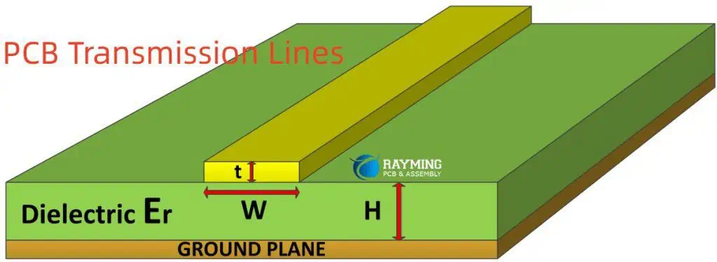
Transmission lines like microstrips and striplines carry high frequency signals across a PCB:
Matched Impedance
Use controlled impedance lines matched to system impedance (typically 50 ohms) to minimize losses.
Short Stub Lines
Keep stubs short to avoid unwanted capacitive coupling. Use vertical transitions where changes are unavoidable.
Smooth Wave Impedance
Taper impedance gradually over longer lengths for impedance matching and reduced reflections.
Terminate Lines
Properly terminate lines in their system impedance at the load end to prevent reflections from discontinuities.
Reflection-Free Bends
Avoid 90 degree bends. Use arc or mitered 45 degree bevels to reduce discontinuities in the wave impedance.
Coupled Lengths
When coupling lines, tightly control the gap and length ratio to achieve target coupling factors.
Careful application of transmission line theory is critical to RF PCB performance.
Grounded Coplanar Waveguides
Grounded coplanar waveguides involve placing signal traces between ground planes on the same layer. Benefits include:
- Excellent shielding and isolation
- Permits closer packing density
- Reduces radiation losses
- Allows easy shielding vias to ground
- Supports high frequency millimeter-wave signals
Use coplanar techniques where stripline or microstrip won’t suffice for shielding or density needs.
Passive Components
RF passives require special attention during layout:
Place Near ICs
Keep passives physically close to their driving IC pins to avoid long stub traces.
Orient Perpendicular
Wherever possible, orient inductors and capacitors perpendicular to their attached traces. This avoids parasitics.
Flood Ground Around
Provide a flood ground fill around all passive components. This shields noise coupling and maintains low inductance.
Watch Spacing
mind spacing around passives to avoid coupling between components.
Model Libraries
Use vendor 3D models or EM-based parasitic models for passives for optimal simulation accuracy.
Careful passive layout minimizes parasitic effects that impair frequency response.
Material Selection

Choosing suitable PCB materials is crucial for achieving target RF performance. Key considerations include:
Dielectric Constant
Select a dielectric constant to ensure proper impedance. Variability risks impedance mismatches.
Loss Tangent
Lower loss materials like PTFE reduce insertion losses for greater range and efficiency.
Moisture Absorption
Lower absorption coefficients minimize performance degradation in humid conditions.
Thermal Properties
Manage lamination stresses and match expansion coefficients to avoid electrical issues from physical warping.
Lead-Free Assembly
Use high Tg materials compatible with lead-free assembly processes necessary for commercial products.
Availability
Choose readily available materials with multiple qualified laminators to control supply chain risks.
There are always tradeoffs to weigh when selecting RF laminates.
Copper and Finishes
Like dielectrics, carefully selecting conductor materials enhances RF response:
Copper Weights
Heavier copper above 2 oz enables better power handling and low loss performance.
Rolled or Electrodeposited
Electrodeposited copper foils tend to provide smoother surface finishes.
Surface Roughness
Smooth copper foil reduces conductor losses at high frequencies due to skin effects.
Final Finish
Immersion silver or gold provide excellent surface conductivity while slowing tarnishing.
Plating Buildup
For heavy power traces, electroplated copper increases conductor thickness over foil alone.
Thermal Management
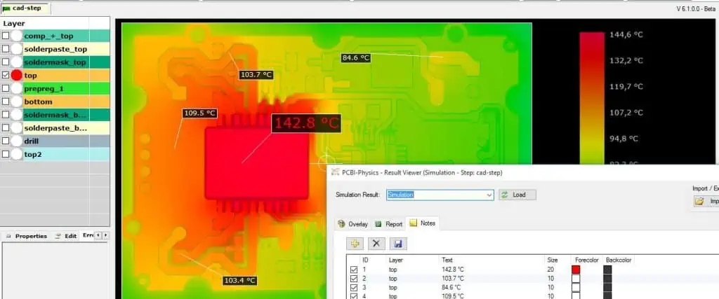
Poor thermal performance impacts RF PCBs through:
- Electrical parameter variations with temperature
- Mechanical warping inducing stress
- Accelerated aging and material breakdown
Use Thermal Vias
Place thermal vias under hot components allowing heat conduction to inner and bottom layers.
Flood Planes
Use thick copper plane layers as heat spreaders where possible.
Heatsinks
Add localized heatsinks under high power devices if needed.
Air Flow
Permit sufficient air flow for convection cooling during enclosure design.
Thermal Modeling
Model thermal performance early to identify hotspots and refine layouts.
Proper thermal design prevents fluctuations and damage over the operating life.
Simulations
Accurately simulating RF boards requires using the appropriate tools:
EM Simulators
Full wave 3D EM simulation captures complex energy interactions between components.
Parasitic Extractors
Model detailed parasitic characteristics caused by pads, vias, traces, and ground planes.
Material Models
Leverage available laminate material models from manufacturers capturing frequency dependent performance.
PCB PDN Analysis
Analyze common and differential path impedances to predict noise coupling on board.
S-Parameters
Use s-parameters for components to capture frequency-based input/output behavior.
TDR Modeling
Time domain TDR simulation validates impedance control and dispersion.
Matching simulations to real measured results builds confidence in the PCB layout.
Conclusion
Following sound RF design principles enables PCBs operating reliably at microwave and mmWave frequencies. Paying attention to stackup arrangements, layout techniques, material selections, simulations, and other best practices prevents nasty surprises late in the development cycle. While RF design requires meticulous care, the methodical application of these guidelines results in high performance boards meeting their operating goals across all conditions.
Frequently Asked Questions
Q: At what frequency do RF design considerations for PCBs start to become necessary?
A: Most experts recommend treating any design over 1 GHz as an RF layout. However, techniques help even at a few hundreds MHz.
Q: What are some key software tools used for RF PCB design and simulation?
A: Popular options include Cadence Allegro, Mentor Xpedition, Keysight ADS, Ansys HFSS, and Altium.
Q: What are typical stackup layer counts for RF PCB designs?
A: High frequency boards trend towards 4-16 layers. This enables embedding controlled impedances between ground planes while avoiding overly thick dielectrics.
Q: How are impedance matched interconnects created on PCBs?
A: Carefully engineering the trace geometry and dimensions along with dielectric height relative to ground maintains target impedance like 50 ohms across a route.
Q: What are some common RF PCB laminate materials?
A: Popular options include Rogers RO4000, Taconic RF-35, Isola IS680, Arlon CLTE, and PTFE composites. These provide tightly controlled dielectric constants.

