Introduction
In today’s digital age, Printed Circuit Boards (PCBs) are the backbone of nearly every electronic device we use. From smartphones to satellites, PCBs play a crucial role in connecting and supporting electronic components. Understanding the PCB manufacturing process is essential for engineers, designers, and anyone involved in the electronics industry. This comprehensive guide will walk you through the intricate steps of PCB manufacturing, providing insights into the technology, challenges, and best practices in this field.
What is PCB Manufacturing?

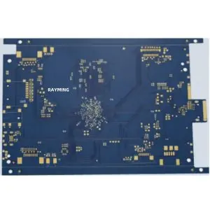
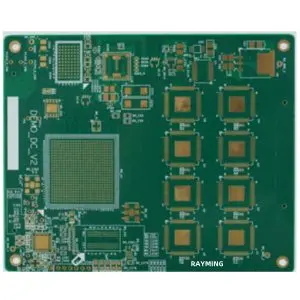
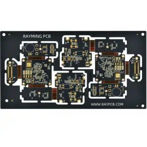
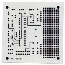
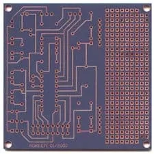
PCB manufacturing is the process of creating printed circuit boards that mechanically support and electrically connect electronic components using conductive pathways, tracks, or signal traces etched from copper sheets laminated onto a non-conductive substrate. This process involves multiple steps, combining precision engineering, chemistry, and advanced technology to produce boards that meet the exacting standards of modern electronics.
Learn More about:
- PCB Assembly Process
- Flex PCB Manufacturing Process
- Rigid Flex PCB Manufacturing Process
- Ceramic PCB Manufacturing Process
- Aluminum PCB Manufacturing Process
Key Aspects of PCB Manufacturing:
- Substrate Material Selection: Choosing the right base material, typically FR-4 (a glass-reinforced epoxy laminate).
- Copper Layering: Applying thin copper foils to the substrate.
- Circuit Design Transfer: Transferring the designed circuit pattern onto the copper layers.
- Etching: Removing unwanted copper to create the circuit paths.
- Layering: For multi-layer boards, bonding multiple layers together.
- Drilling: Creating holes for component connections and vias.
- Surface Finishing: Applying protective coatings and final touches.
Now, let’s dive into the detailed steps of the PCB manufacturing process.
PCB Manufacturing Process – 22 Steps

Step 1: Design and Output
The PCB manufacturing process begins with the design phase. Engineers use Computer-Aided Design (CAD) software to create the circuit layout. This design is then converted into a format that manufacturing equipment can understand, typically Gerber files.
Key Points:
- Circuit schematic creation
- Component placement and routing
- Design Rule Check (DRC)
- Generation of Gerber files and drill data
Step 2: PPE – Pre Production Engineering
Before actual production begins, the design undergoes a thorough review to ensure manufacturability and to identify any potential issues.
Activities in PPE:
- Design for Manufacturing (DFM) check
- Stack-up design for multi-layer boards
- Panelization planning
- Tool and process selection
Step 3: From File to Film
In this step, the digital design is transferred to a physical film, which serves as a template for creating the circuit pattern on the PCB.
Process Details:
- Photoplotter usage for film creation
- Negative or positive image generation based on design requirements
- Film inspection for accuracy
Step 4: Board Cutting (Copper Clad Laminate Cutting)
Raw PCB material, typically copper-clad laminate, is cut to the required panel size.
Considerations:
- Precision cutting to ensure correct dimensions
- Material handling to prevent damage or contamination
Step 5: Printing the Inner Layers
For multi-layer PCBs, this step involves creating the internal circuit layers.
Techniques Used:
- Photoresist application
- UV light exposure through the film mask
- Development of the photoresist
Step 6: Etch Inner Layers

Unwanted copper is removed from the inner layers through chemical etching.
Etching Process:
- Chemical bath application
- Controlled etching to maintain circuit integrity
- Removal of remaining photoresist
Step 7: Inner Layer Alignment
Ensuring precise alignment of inner layers is crucial for multi-layer PCBs.
Alignment Methods:
- Optical alignment systems
- Registration hole punching
- Layer stack-up preparation
Step 8: Automatic Optical Inspection (AOI) Inspection
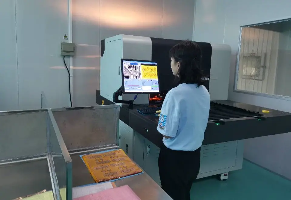
Each inner layer undergoes AOI to detect any defects or inconsistencies.
Inspection Criteria:
- Circuit pattern accuracy
- Copper trace width and spacing
- Absence of shorts or opens
Step 9: Layer-up and Bond
For multi-layer PCBs, the individual layers are stacked and bonded together.
Bonding Process:
- Layer stacking with prepreg sheets
- Application of heat and pressure in a lamination press
- Curing to create a solid multi-layer board
Step 10: Drilling the PCB
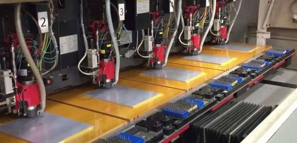
Holes are drilled for component leads, vias, and mounting purposes.
Drilling Techniques:
- CNC drilling for precision
- Laser drilling for micro vias
- X-ray drilling for buried vias in multi-layer boards
Step 11: Plating and Copper Deposition
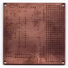
This step involves depositing a thin layer of copper over the entire board, including the drilled holes.
Plating Methods:
- Electroless copper deposition
- Electrolytic copper plating
- Through-hole plating for electrical connectivity
Step 12: Outer Layer Imaging
Similar to inner layer imaging, the outer layer circuit pattern is created.
Imaging Process:
- Dry film lamination
- UV exposure using artwork
- Development of the resist pattern
Step 13: Plating
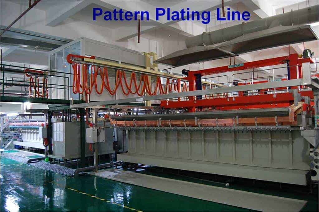
Additional copper is plated onto exposed areas to build up the required copper thickness.
Plating Considerations:
- Copper thickness requirements
- Uniform plating distribution
- Plating of surface mount pads
Step 14: Etch Outer Layer
Unwanted copper is removed from the outer layers, leaving the desired circuit pattern.
Etching Techniques:
- Chemical etching
- Mechanical etching for fine-line requirements
- Differential etching for varied copper thicknesses
Step 15: Outer Layer AOI
Another round of AOI is performed to ensure the accuracy of the outer layer circuits.
Inspection Focus:
- Circuit pattern integrity
- Copper thickness uniformity
- Absence of under-etching or over-etching
Step 16: Solder Mask Application

A protective layer is applied to insulate the copper traces and prevent solder bridges.
Solder Mask Process:
- Solder mask ink application
- UV curing
- Development to expose pads and vias
Step 17: Surface Finish
Various finishes are applied to protect exposed copper and enhance solderability.
Common Finishes:
- Hot Air Solder Leveling (HASL)
- Electroless Nickel Immersion Gold (ENIG)
- Immersion Tin
- Organic Solderability Preservative (OSP)
Step 18: Silkscreen Printing

Component designators, logos, and other markings are printed on the board.
Silkscreen Considerations:
- Ink type selection
- Curing process
- Alignment with board features
Step 19: Electrical Test

Each board undergoes electrical testing to ensure proper connectivity and isolation.
Testing Methods:
- Flying probe testing
- Bed of nails testing
- Continuity and isolation checks
Step 20: Profiling and V-Scoring
Boards are cut to their final shape, and V-scoring is applied for easy separation of panelized boards.
Profiling Techniques:
- CNC routing
- Laser cutting for precision requirements
- V-groove scoring for break-apart panels
Step 21: Final Inspection
A thorough visual and functional inspection is performed before packaging.
Inspection Points:
- Physical dimensions
- Surface finish quality
- Silkscreen accuracy
- Overall board integrity
Step 22: Packaging
Boards are carefully packaged to protect them during shipping and storage.
Packaging Considerations:
- Moisture-sensitive packaging for certain finishes
- ESD protection
- Proper labeling and documentation
2 Layer Vs. Multilayer Manufacturing Process
While the basic principles remain the same, there are significant differences between manufacturing 2-layer and multilayer PCBs.
2-Layer PCB Manufacturing:
- Simpler process with fewer steps
- No inner layer processing required
- Generally faster and more cost-effective
Multilayer PCB Manufacturing:
- More complex with additional steps for inner layers
- Requires precise layer alignment and bonding
- Involves advanced techniques for buried and blind vias
- Offers higher circuit density and better EMI shielding
What is the Difference Between PCB Manufacturing and PCB Assembly Process?
It’s important to distinguish between PCB manufacturing and PCB assembly, as they are two distinct processes in creating a functional electronic device.
PCB Manufacturing:
- Focuses on creating the bare PCB
- Involves all steps from design to final board production
- Ends with a bare board ready for component mounting
PCB Assembly:
- Begins with a completed bare PCB
- Involves placing and soldering components onto the board
- Includes processes like solder paste application, component placement, reflow soldering, and testing of the assembled board
8 Best DFM Tips for PCB Manufacturing

Design for Manufacturing (DFM) is crucial for ensuring smooth production and high-quality PCBs. Here are eight essential DFM tips:
- Optimize Trace Widths and Spacing: Adhere to manufacturer capabilities for minimum trace width and spacing.
- Consider Copper Pour: Use copper pours for ground planes and improved thermal management.
- Plan Via Placement Carefully: Avoid vias in pads when possible and use appropriate via sizes.
- Mind the Edge Clearance: Leave sufficient space between components and board edges.
- Use Standard Drill Sizes: Stick to standard drill sizes to reduce manufacturing costs.
- Consider Panelization: Design with panelization in mind for efficient production.
- Implement Proper Silkscreen Design: Ensure silkscreen text is readable and doesn’t overlap with solder mask openings.
- Follow Stack-up Guidelines: Work with your manufacturer to design an appropriate layer stack-up for multilayer boards.
Trends and Challenges in PCB Manufacturing Technology
The PCB manufacturing industry is constantly evolving, driven by advancements in technology and changing market demands.
Current Trends:
- Miniaturization: Increasing demand for smaller, denser PCBs.
- Flexible and Rigid-Flex PCBs: Growing popularity in wearable and IoT devices.
- High-Frequency Materials: Adoption of advanced materials for 5G and high-speed applications.
- Additive Manufacturing: Exploration of 3D printing technologies for PCB production.
- Green Manufacturing: Focus on environmentally friendly processes and materials.
Challenges:
- Increasing Complexity: Managing the complexity of high-density interconnect (HDI) boards.
- Material Limitations: Overcoming the limitations of traditional PCB materials.
- Cost Pressures: Balancing cost-effectiveness with advanced manufacturing requirements.
- Quality Control: Maintaining high quality standards with increasing miniaturization.
- Skilled Labor Shortage: Addressing the need for skilled technicians in advanced PCB manufacturing.
Conclusion
The PCB manufacturing process is a complex, multi-step journey that transforms a simple design into a sophisticated electronic component. From the initial design phase to the final packaging, each step requires precision, expertise, and attention to detail. As technology continues to advance, PCB manufacturers must adapt to new challenges while maintaining the high standards of quality and reliability that modern electronics demand.
Understanding this process is crucial for anyone involved in electronics design or production. By following best practices in Design for Manufacturing and staying abreast of industry trends, engineers and manufacturers can ensure the production of high-quality, cost-effective PCBs that meet the ever-evolving needs of the electronics industry.
As we look to the future, the PCB manufacturing process will undoubtedly continue to evolve, driven by the relentless pursuit of smaller, faster, and more efficient electronic devices. The industry’s ability to innovate and overcome challenges will play a crucial role in shaping the next generation of electronic products that will power our increasingly connected world.