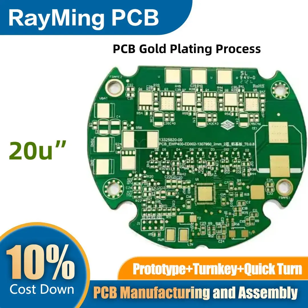
The 20μ” (20 microinches) PCB Gold Plating Process refers to a specific technique used in printed circuit board manufacturing to deposit a thick layer of gold onto copper surfaces. This process, often called hard gold plating, involves several steps:
-
Cleaning: The PCB is thoroughly cleaned to remove any contaminants.
-
Activation: The copper surface is activated to improve adhesion.
-
Nickel plating: A layer of nickel is electroplated onto the copper, typically 50-150μ” thick.
-
Gold plating: A 20μ” layer of gold is electroplated over the nickel.
This thick gold layer offers several advantages:
- Excellent wear resistance for high-reliability connectors
- Superior conductivity for critical signal paths
- Exceptional corrosion resistance for harsh environments
- Ideal for applications requiring multiple insertion cycles
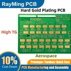
The 20μ” thickness is significantly more than standard ENIG finishes, making it suitable for high-performance applications in aerospace, military, and telecommunications industries. However, it’s more expensive than thinner gold finishes, so it’s typically used only where necessary for performance or reliability reasons.