Designing the layout and circuitry of a printed circuit board (PCB) is a key step in developing an electronic product. The PCB provides the foundation for component assembly and enabling system operation. For those new to PCB design, the process can seem intimidating at first. However, by following a step-by-step approach, even beginners can learn the fundamentals of PCB design.
This article provides 16 easy steps to guide you in getting started with designing simple PCBs quickly.
Step 1: Have a Clear Design Idea
Design a circuit board
Define the electronic product or device you want to build. This provides the requirements for the PCB design.
Research similar products and circuits to guide the architecture.
List out the key functions and components needed.
Having a clear design concept is vital before jumping into the PCB layout software.
Step 2: Select the Core Components
Make a list of the major ICs and other critical components like microcontrollers, sensors, connectors etc.
These provide the core functionality and drive the design.
Check availability, datasheets, footprints and pricing.
Order samples for prototyping.
Choosing the key components early provides a framework for the PCB design process.
Use online PCB services for affordable quickturn prototyping.
Review quoted costs and lead times before ordering.
Share manufacturing files.
Test circuits with actual boards instead of just software simulations.
Step 16: Assemble and Test Boards
With the PCB prototypes received, populate components following BOM.
Test power-up, voltages, signals and intended functionality.
Update design as needed to rectify any issues observed.
Thoroughly testing prototype boards verifies the design and avoids costly mistakes.
Conclusion
The prospect of designing a PCB from concept to completion can seem daunting for beginners. By following a structured, step-by-step approach, breaking down the design into smaller logical blocks, and leveraging the right software tools, even amateurs can get started with simple PCB layout and circuit design quickly. Hands-on testing of prototypes is key to progressively building up expertise. With practice, new designers gain the experience needed to bring more advanced electronic product ideas to fruition.
Key Takeaways
Have a clear design idea and requirements before starting
Select the core components early to guide design
Leverage reference designs to accelerate learning
Use beginner-friendly PCB design software
Develop the schematic diagram first visually
Include power supply, bypass capacitors and supporting components
Follow design rules and PCB capabilities
Add identifying silkscreen markings and labels
Verify all outputs before manufacturing release
Test prototypes to validate the design
Recommended Next Steps
To take your PCB design skills further:
Create more advanced circuits using sensors, communication ICs, high speed interfaces etc.
Learn key principles like impedance control, thermal management, EMI/ESD protection etc.
Get familiar with your PCB manufacturer’s capabilities and process limitations
Experiment with more complex component packages like BGAs
Study example designs across various applications and circuits
Join PCB design communities to connect with experts
With diligent practice and an systematic approach, PCB design skills can be readily developed.
Antennas are a vital component in any wireless system, serving as the interface between the electronic circuitry and open air. With wireless capabilities becoming ubiquitous across consumer, automotive, medical, defense and industrial applications, antenna design has taken on increased importance. This article provides key guidelines and considerations for engineers designing and integrating antennas for printed circuit board (PCB) applications.
Topics covered include:
Fundamentals of antenna specifications
Basic antenna theory and types
Matching network design principles
Guidelines for integrating antennas on PCBs
RF layout techniques for antennas
Considerations for antenna arrays
Testing and measuring antenna performance
Real-world antenna integration examples
Tips for antenna design success
By understanding antenna design principles and following RF PCB layout best practices, engineers can help ensure excellent connectivity, efficiency and reliability for wireless systems.
This provides an overview of antenna varieties commonly integrated into PCB designs. The choice depends greatly on the radiation pattern, polarization, bandwidth, gain, and efficiency required. Each antenna type has advantages and disadvantages that must be weighed against application needs.
Arraying multiple antennas on a PCB provides benefits like higher gain, electronic beam steering, and pattern diversity. Key array design considerations include:
Gain Enhancement
More elements increases antenna gain
But mutual coupling effects must be accounted for
Beam Steering
Varying phase between elements rotates beam direction
Permits rapid electronic scan without physical movement
Resonance Control
Interactions between arrayed elements changes impedance
May require larger matching network, isolation structures
Pattern Optimization
Spacing between elements shapes overall pattern
Wider separation broadens beamwidth
Layout Symmetry
Equal spacing between identical elements
Maintains uniform characteristics for phased arrays
Isolation Structures
Prevent coupling between elements
Trenches, neutralization lines, parasitic elements
By applying sound array design principles, multiple antennas on a PCB can work cooperatively to produce tailored performance exceeding single elements.
Testing and Measuring Antenna Performance
Evaluating antenna parameters on an assembled PCB requires specialized measurement techniques:
Impedance
Vector network analyzer scans impedance versus frequency
Confirms proper matching at desired band
Reflection Coefficient
Measures power reflected from antenna due to mismatch
Minimized by antenna-feed impedance alignment
Radiation Pattern
Conducted in anechoic chamber or open field
Record signal strength versus spherical or planar angle
Directivity and Gain
Comparative measurements using reference antenna
Remove effects of mismatch loss
Efficiency
Measure input and radiated power to determine losses
Assess effects of nearby components
Careful antenna testing validates design simulations and ensures all specifications are satisfied prior to release.
Here are some examples of antenna integration in different wireless systems:
Smartwatch
PCB area constraints necessitated compact monopole antenna
Matched to 50 ohms using L-section network
Quarter-wave length selected for 2.4GHz Bluetooth band
Orientation parallel to watch band for omnidirectional pattern
Automotive RADAR PCB
Four patch antennas arrayed for beam steering
Microstrip feed lines with tuned isolation trenches
Integrated into 24GHz RADAR transceiver PCB
Broadside directional pattern oriented forward
Wearable Medical Sensor
Meandered inverted-F antenna (MIFA) for size reduction
Resonant at 915MHz ISM band for sensor data links
Flexible antenna on flexible PCB conforms to skin
Ground plane shields antenna from body
These examples illustrate how antenna integration must be tailored to the specific constraints and use cases of each wireless system.
Tips for Successful On-Board Antenna Design
Here are some useful tips to help guide the antenna design and integration process:
Clearly identify key electrical specs like frequency, bandwidth, gain patterns
Select antenna topology suited to physical constraints
Model antenna behavior with electromagnetic simulation
Design matching network early once antenna selected
Carefully position antenna considering isolation needs
Review impact of nearby components like batteries or processors
Verify final performance through antenna pattern and network analysis measurements
Build and test prototypes to characterize real-world effects
Iterate on design based on measured results
By following a structured design flow, RF engineers can overcome the difficulties of on-board antenna integration to achieve wireless connectivity objectives.
Frequently Asked Questions
Here are some common FAQs regarding PCB antenna design:
Q: What are some good antenna options for a small wearable device?
Compact monopoles, loops, helices and meandered antennas are good options. Ensure adequate ground plane clearance for proper radiation.
Q: How early should antenna design be started in the development process?
Ideally during the concept phase so size and placement can inform early PCB layout. Retrofitting antenna design late causes compromises.
Q: What are some techniques to reduce coupling between multiple antennas?
Physical separation, ground trenches, neutralization lines and orienting orthogonally help isolate closely spaced antennas.
Q: How can I estimate the transmission line impedance needed to match my antenna?
Tools like Smith charts allow converting from complex antenna impedance to appropriate real transmission line impedance for a given matching network.
Q: What should I look out for when testing an integrated PCB antenna?
The effects of antenna proximity to the PCB and nearby components. Performance often differs significantly from isolated simulations.
Conclusion
On-board antenna integration presents challenges but following sound design practices enables robust wireless connectivity in the smallest products. As antennas become ubiquitous across virtually all electronics, mastering antenna design and layout flows is an invaluable skill for modern electrical engineers. The guidance provided throughout this article aims to equip PCB designers with the key principles and best practices to unlock the full potential of integrated antenna solutions.
1.Introduction
Antenna PCB design and RF layout are critical in a wireless system that transmits and receives electromagnetic radiation in free space. The wireless range that an end-customer gets out of an RF product with a current-limited power source such as a coin-cell battery depends greatly on the antenna design, the enclosure, and a good PCB layout. It is not uncommon to have a wide variation in RF ranges for designs that use the same silicon and the same power but a different layout and antenna-design practice. This application note describes the best practices, layout guidelines, and an antenna-tuning procedure to get the widest range with a given amount of power. Other important general layout considerations for RF trace, power supply decoupling, via holes, PCB stackup, and antenna and grounding are also explored. The selection of RF passives such as inductors and capacitors is covered in detail.
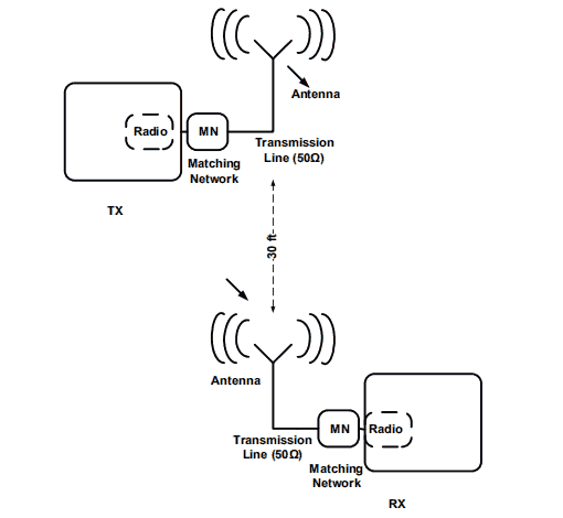
Each topic ends with tips or a checklist of design items related to the topic. Figure 1 shows the critical components of a wireless system, both at the Transmitter (TX) and Receiver (RX). Figure 1. Typical Short-Range Wireless Syst
Typical Short-Range Wireless Syst
A well-designed antenna ensures optimum operating distance of the wireless product. The more power it can transmit from the radio, the larger the distance it can cover for a given packet error rate (PER) and receiver sensitivity. Similarly, a well-tuned radio at the receiver side can work with minimal radiation incident at the antenna. The RF layout together with the radio matching network needs to be properly designed to ensure that most of the power from the radio reaches the antenna and vice versa
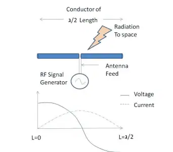
An antenna is basically a conductor exposed in space. If the length of the conductor is a certain ratio or multiple of the wavelength of the signal1, it becomes an antenna. This condition is called resonance‖, as the electrical energy fed to antenna is radiated into free space. Figure 2. Dipole Antenna Basic
Dipole Antenna Basic
feeds the antenna at its center point by a transmission line known as ―antenna feed. At this length, the voltage and current standing waves are formed across the length of the conductor, as shown in Figure 2. The electrical energy input to the antenna is radiated in the form of electromagnetic radiation of that frequency to free space. The antenna is fed by an antenna feed that has an PCB impedance of, say, 50 Ω, and transmits to the free space, which has an impendence of 377 Ω2 . Thus, the antenna geometry has two most important considerations: 1. Antenna length 2. Antenna feed The /2-length antenna shown in Figure 2 is called a dipole antenna. However, most antennas in printed circuit boards achieve the same performance by having a /4-length conductor in a particular way. See Figure 3. By having a ground at some distance below the conductor, an image is created of the same length (/4). When combined, these legs work like a dipole antenna. This type of antenna is called the quarter-wave (/4) monopole antenna. Most antennas on the PCB are implemented as quarter-wave antennas on a copper ground plane. Note that the signal is now fed single-ended and that the ground plane acts as the return path.
Figure 3. Quarter-Wave Antenna
Quarter-Wave Antenna
For a quarter-wave antenna that is used in most PCBs, the important considerations are:
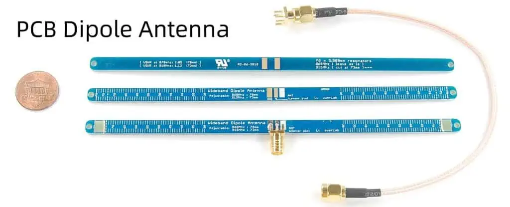
1. Antenna length 2. Antenna feed 3. Shape and size of the ground plane and the return path 3 Antenna Types As described in the previous section, any conductor of length /4 exposed in free space, over a ground plane with a proper feed can be an effective antenna. Depending on the wavelength, the antenna can be as long as the FM antenna of a car or a tiny trace on a beacon. For 2.4-GHz applications, most PCB antennas fall into the following types: 1. Wire Antenna: This is a piece of wire extending over the PCB in free space with its length matched to /4 over a ground plane. This is generally fed by a 50-Ω 4 transmission line. The wire antenna gives the best performance and RF range because of its dimensions and three-dimensional exposure. The wire can be a straight wire, helix,or loop. This is a three-dimensional (3D) structure, with the antenna over a height of 4-5 mm over the PCB plane,protruding into space.
Figure 4: Wire Antenna
Wire Antenna
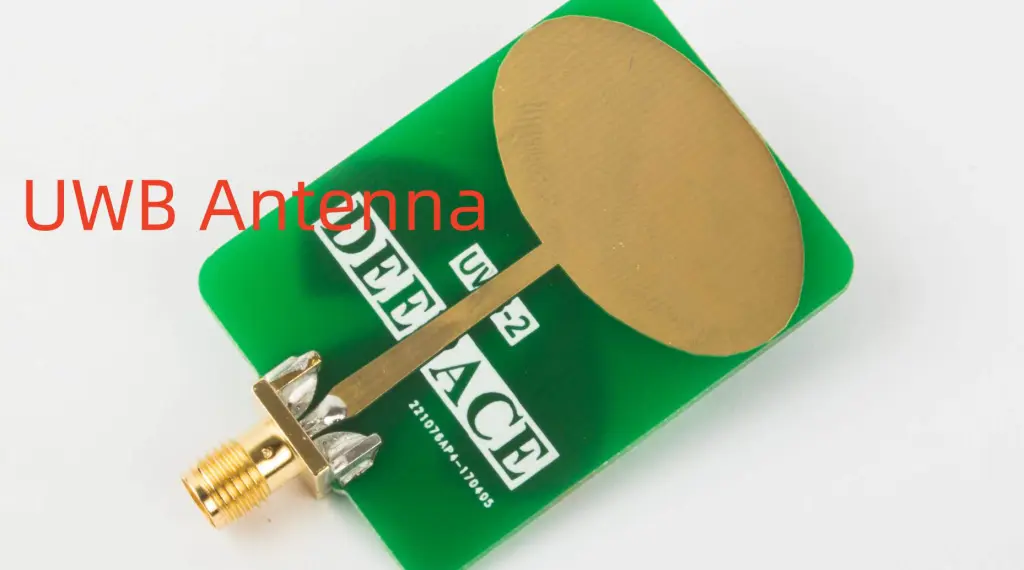
2. PCB Antenna: This is a trace drawn on the PCB. This can be a straight trace, inverted F-type trace, meandered trace, circular trace, or a curve with wiggles depending on the antenna type and space constraints. In a PCB antenna, the antenna becomes a two-dimensional (2D) structure in the same plane of the PCB; see Figure 5.There are guidelines 5 that must be followed as the 3D antenna exposed in free space is brought to the PCB plane as a 2D PCB trace. A PCB antenna requires more PCB area, has a lower efficiency than the wire antenna,but is cheaper. It has easy manufacturability and has the wireless range acceptable for a BLE application.
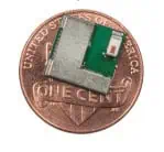
3. Chip Antenna: This is an antenna in a small form-factor IC that has a conductor packed inside. This is useful when there is limited space to print a PCB antenna or support a 3D wire antenna. Refer to Figure 6 for a Bluetooth module containing a chip antenna. The size of the antenna and the module in comparison with a one cent is coin is given below. Figure 6. Cypress EZ BLE Module (10 mm × 10 mm) with Chip Antenna
Cypress EZ BLE Module (10 mm × 10 mm) with Chip Antenna
Next Part We will take about how to Choosing an Antenna.
IC Unlock, IC Crack and IC Decipher – All You Need to Know
Rayming continues to be recognized as the Southern China Leader in Services for IC Clone, MCU Crack, Microcontroller Unlock service. With the advancement of today’s modern circuit board technology, it is more important than ever to have specialists available to help you at a moment’s notice. Our engineering and commercial teams collectively have a vast amount of electronic experience covering field include Consumer Electronics, Industrial Automation Electronics, Wireless Communication Electronics., etc. For more information please contact us through email: Sales@raypcb.com
We have more than 100 software and hardware rich experience expert for chip decryption, IC Crack, MCU unlock, IC reverse analysis/ ASM Code, chip burnish and model identification, PCB cloning and mass production.We have a shocking price advantage and success rate. Proficient in medical and health equipment, industrial control equipment and game boards clone. Rich experience for chip decryption, quality and price is guaranteed. We can provide the relevant electronic technical support allows customers to assured that doing good product.We always explore others can’t reach areas of technology, and constantly improve our technology service attributes, to help more people realize their riches dream in short-term.
Integrated Circuits are circuits that feature inseparable elements that are electrically interconnected in a way that the IC remains together due to commerce and construction. IC is also known as a microelectronic circuit, chip, or microchip.
The development of IC has changed the electronic industry. It is an important aspect of electronics production. This article discusses all you need to know about IC unlock.
What is IC Unlock?
IC unlock refers to the decryption of the IC via the semiconductor reverse engineering methods. After IC unlocking, the program of the integrated circuits becomes readable. IC unlock is also referred to as IC decryption, IC crack, or IC attack. IC unlock is an important step in PCB cloning. To clone a printed circuit board, it is important you do IC crack.
How to Unlock an Integrated Circuit
To unlock IC, there are different approaches. Some of these methods will be discussed here;
Electronic detection cracks
In this approach, the technology monitors the analog attributes of all interface and power connections of the processor. This is done during usual operation at high resolution by checking its electromagnetic radiation attributes. There is a change in the power consumption as it carries out different instructions since the microcontroller is also a functional electronic device.
This enables the attacker to get critical detail in the microcontroller through the detection and analysis of these changes. To achieve this, electronic measuring instruments are used. The radio frequency programmer can read the encryption MCU program’s old model.
UV attack method
This method simply utilizes UV radiation on the chip and then transforms this chip into a non-encrypted chip. The programmer will then directly read the program. This approach is ideal for OTP chips. Engineers specialized in microcontrollers design understand that only UV light can erase OTP chips.
Therefore, UV is used to remove encryption. UV light can irradiate this type of IC directly. It is important the chip is opened first if the package is plastic. Since the encryption of this chip is poor, no cost is required for the basic decryption. This makes the cost of the chip decryption very cheap.
Software attacking
This approach utilizes the exploit protocols and processor communication interfaces to fight the IC. The attack on the ATMELAT89C family of microcontrollers is an example of a software attack. The attacker utilized a designed program, preventing the next step of eliminating the memory data of the program.
The program turned out to be non-encrypted. The encryption methods can also be used to attack integrated circuits depending on the new attacking device’s development.
FIB recovery encryption fuse method
This is another method of unlocking IC. It is an ideal method for chips having fuse encryption. TI’s MSP430 cracking is a good example. Since the MSP430 encryption is meant for burning fuse, the IC becomes non-encrypted chips. The probe is normally utilized to get the fuse re-connection.
This can be achieved by change lines that contract to semiconductor modification industries. The focused ion beam (FIB) equipment can be used to connect the line. However, this method isn’t really ideal since the demands for consumables and equipment increase the cost of IC unlock work.
Error generation attack technology
To unlock an IC, this technology utilizes unusual operating conditions to make processor errors and the processor gives more access to allow the attacks. Clock strikes and voltage are the errors generation technologies that are commonly used.
High-voltage and low-voltage attacks can help to disable the shield to circuit or make the processor forcefully carry out incorrect operations. The protection circuitry may reset without disturbing the protected data by using a clock transition. Clock and power transitions can have an impact on the execution and decoding of instruction in some processors.
Chip loopholes
IC circuit can be unlocked using chip loopholes. Several chips are cryptographically vulnerable during design time. These types of chips can take advantage of vulnerabilities to force the chip to read out the code in memory. The program can be reversed if the continuous FF code can be found.
Furthermore, the chip has some obvious loopholes when including the electronic signal, like a pin in the encryption becoming a non-encrypted chip. To achieve IC unlock, today’s chip decryption devices use the loopholes in the program or the chip.
Adjusting the encryption circuit
DSP and CPLD designs are complicated. This method could be difficult to carry out decryption. It is important to analyze the structure of the chip and then identify the encryption circuit. The chip circuit adjusting equipment can be used to make some changes.
Probe technology
In this type of approach, the chip internal connections are directly exposed. The technology then studies, interacts, manipulates the microcontroller to accomplish the attack’s purpose. IC unlock is related to MCU reverse engineering.
The price of IC crack defers and this depends on the model. It is important to know that the price of IC unlock is related to expenses incurred on it. The decryption price is higher when the cost of the solution is higher. The cost of developing solutions varies for different companies. This is due to their technical strength.
The payment of IC crack depends on the requirements and situation of the customer. Payments can be made through PayPal service, Bank, and western union. The disadvantage of PayPal service is the high handling fee. The price of the seller is often charged by 5 percent.
This type of integrated circuit functions by attacking continuous signals. It can perform tasks like modulation, filtering, demodulation, and amplification. Examples of Analog ICs include OP-AMP’s, RF ICs, Sensors, and Linear ICs
Digital IC features two levels which are 0’s and 1’s. This means that it uses binary mathematics where 0 means off and 1 means on. This type of IC is achieved when they include millions of whatnot, flip flops, and logic gates. Microprocessors and microcontrollers are good examples of digital integrated circuits.
Mixed signal
An integrated circuit is mixed-signal when both analog and digital ICs are utilized on a chip. Examples of mixed ICs include clock or timing ICs and data acquisition ICs.
Benefits of ICs
Integrated circuits have several benefits. They feature millions of electronic components like capacitors, resistors, and transistors which are fixed into a chip. Almost all devices use IC due to their size and reliability. Devices such as mobile phones, digital watches, and Televisions use integrated circuits. ICs help electronic devices work in good condition.
ICs have improved performance and operating speed which make them ideal for small signal operation. These circuits are reliable and consume less power. They are small in size and more consistent. Integrated circuits are also known for operating at extremely high temperatures. IC cracker also has its benefits
They have the ability to withstand high temperatures. Due to these benefits, they are used in applications like memory devices, video processors, radar, logic devices, audio amplifiers, etc.
IC Unlock Services – What do they do?
An IC unlock service helps you to crack your IC sample. Your IC program will be given out in the Bin/Hex file. This service will decap IC sample and the sample won’t work again after you break IC.
IC services feature unlockable models like Lattice/ TMS/ AT/ DSP56/ STM and more. To get your pricing for IC crack, you will need to send the correct IC model to prepare a quotation. Some of these services allow 50 percent payment to begin the project.
IC crack can begin after initial and sample payment has been received. After the customer has tested the project, the IC unlock service receives the remaining 50% payment. Most IC unlock services work with stringent rules and regulations.
Frequently Asked Questions
Can IC be returned after IC crack has been done?
The integrated circuit can’t be returned. After IC unlock, IC cap would have been opened. So, the technology used will be exposed from the integrated circuit.
What file is given to the customer once the IC has been unlocked? Immediately the IC has been unlocked, the customer will get a Binary file. This file can be burned into the integrated circuit via a programmer to allow the IC to remain in working condition. If the customer needs an assembler code file, then a reverse compiling tool is required.
How long does it take to do IC crack? Normally, IC unlock can be done within 10-50 minutes. However, it can take longer than this. This depends on certain factors. Some IC unlock services rent laboratories from third parties.
Can the IC be reused after the IC break?
Some integrated circuits need focused ion beam technology to decode them. This technology uses decapsulation. This procedure makes the IC not fit to be reused after the unlock has been done. If the IC decoding utilizes software, these integrated circuits can be reused after unlock.
Conclusion
IC unlock refers to decrypting integrated circuits using the semiconductor reverse engineering methods. After the IC has been cracked, the programmer can read the program of the integrated circuits. Integrated circuits are very essential in the production of electronics. Therefore, IC unlock should never be overlooked. In this article, we have discussed important things about IC unlock.
We focus on Crack unlock break IC list:
NEC chip crack. UPD78F0515, UPD78F0886, UPD70F3425 and so on. ST MCU code extraction. STM32F103, STM32F105,STM32F207, STM8S103, STM8S003, STM8S903,STM8S105 etc.
Fujitsu chip unlock. MB89F202, MB90F462, MB90F562, MB95F136 and so on. Lattice IC Attack. LC4128V, LC4064V, LC4256C, LC4032V and so on. Mitsubishi chip attack. M30620, M30624, M306N4,M306N5,M30853, M16C10,M16C20 and so on.
Renesas IC unlock. HD64F7047F50v, HD64F3672fpvh8, R5F6456, R5F72544, R5F2136, R5F2134 and so on.
C8051 code unlock crack. C8051F330, C8051F340, C8051F310 and so on. CPLD crack unlock. XC9572XL, XC9536XL, XC95144XL, XC95288, XC95216 and so on. ATMEL series MCU crack. AT89C51,AT89S52, ATMEGA8L, ATMEGA16L, ATMEGA88PA, ATMEGA48PA, AT89C2051, AT88SC0104C etc. DSP chip unlock. TMS320F2812, TMS320F2810, TMS320F2815, TMS320F28335, TMS320F2407, TMS320F240 etc.
Microchip MCU crack. PIC16F883, PIC17C44, PIC18F4220, PIC16F1937, PIC16F1936, PIC18F45K22, PIC18F97J60, PIC18F67K22,PIC18F25K20, PIC18F66K80, PIC18F46K22, pic18F14k22-I/ml, PIC18f46k80,PIC18F24K20,PIC18F4620,PIC18F14K50 and so on. Cypress Chip decryption. CY8C24533, CY8C21534B-24PVXI, CY8C27433, CY8C20346A, CY8C21534B, cy8c3866 and so on. Freescale IC Crack. MC95FG6128AL MC56F84452V MC9S08ACS2 QFP44 MC908JL3E DIP28, mc9s08ac32 MC56F8345 MC56F8322 and so on. Silicon IC Unlock. C8051F001, C8051F002,C8051F300,C8051F301, C8051F410 and so on.
TI IC Code Extraction. MSP430F149, MSP430F1121, M430F5308, M430F1232, M430F5418 etc. NXP Mcu crack. LPC89F932, LPC89F931, LPC89F936, LPC2378FBD144, LPC1114FBD48, LPC2106, LPC2119 and so on.
Altera IC Code Extraction:EPM7128, EPM3064, EPM7192SQC160-15, EPM240, EPM570t100c5n, EPM1270T144C5N etc. Dallas MCU Code extraction. DS2431, DS2432, DS2433, DS1845 and so on.
Holtek IC Crack: HT46R22 HT49R50A, HT46R64, ht46r48a etc.
STC MCU IC unlock.:STC89F516, STC89c52, STC90C58RD,STC90C54RD,STC11F60XE, STC11F02E, STC12c5a60s2, STC12C5410AD, STC10F08XE STC10F12XE, STC10F10XE etc.
Are you looking for reliable PCB clone and PCB copy services? When you have a physical electronic circuit board but lack the original design files, our professional PCB clone service provides the perfect solution. Whether you need PCB copy for obsolete boards or circuit duplication for production scaling, we deliver precision results.
What is PCB Clone and PCB Copy Technology?
PCB clone, also known as PCB copy or PCB duplication, is an advanced reverse engineering technology that creates exact replicas of existing printed circuit boards. Our PCB clone process analyzes your original board and produces identical copies without requiring original design files or Gerber drawings.
Traditional PCB design from scratch involves significant costs including prototype development, testing, and design optimization. Our PCB clone service eliminates these expenses by reverse-engineering existing boards. PCB copy technology reduces development time and costs by up to 70% compared to original design processes.
Our PCB copy services operate within legal frameworks:
Customer ownership verification
Reverse engineering legality
Confidentiality agreements
Ethical business practices
Protecting Your PCB Clone Investment
We safeguard your PCB copy projects through:
Secure data handling
Non-disclosure agreements
Proprietary information protection
Long-term support commitments
Contact Us for PCB Clone Services
Ready to start your PCB clone or PCB copy project? Our expert team provides comprehensive circuit board duplication services with guaranteed quality and fast delivery. Contact us today for a free consultation and discover how our PCB clone expertise can solve your electronic design challenges.
Email: sales@raypcb.comServices: Complete PCB clone and PCB copy solutions Specialties: Multi-layer boards, high-frequency circuits, legacy system replacement
Transform your electronic projects with professional PCB clone and PCB copy services that deliver precision, reliability, and cost-effectiveness.
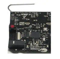
PCB reverse engineering (also known as reverse technology) is a process of printed circuit board design technology reproduction, reverse analysis and research of a target PCB board. It is also to deduce and obtain the design of the product’s processing flow, structure, functional characteristics, and technical specification elements to produce products with similar, but not exactly the same, functions. Reverse engineering originates from hardware analysis in the commercial and military fields. Its primary purpose is to directly analyze the finished product and push out its design principle when the necessary production information cannot be easily obtained.
Another service we offer at RayMing is Printed Circuit Board Reverse Engineering. We can take your sample, including components, and completely reverse engineer it. We create all the data you need to make duplicates. We can even reverse engineer boards that include programmed IC‘s, custom parts, and obsolete parts.
PCB reverse engineering is the process of analyzing and documenting an existing printed circuit board to recreate its schematic diagram and understand its functionality. This technique involves a combination of visual inspection, electrical testing, and advanced imaging technologies to deconstruct the PCB layer by layer, tracing connections and identifying components.
Common Use Cases
PCB reverse engineering finds applications in various scenarios:
Legacy System Repair: When dealing with obsolete or out-of-production systems, reverse engineering can help create documentation for repairs or replacements.
Competitive Analysis: Companies may analyze competitors’ products to understand their design choices and technologies.
Lost Documentation: In cases where original schematics are lost or unavailable, reverse engineering can recreate essential documentation.
Modernization: Updating older designs to incorporate newer technologies or improve efficiency.
Failure Analysis: Investigating the cause of PCB failures in critical systems.
Ethical and Legal Considerations
While PCB reverse engineering is a powerful tool, it’s essential to consider the ethical and legal implications:
Intellectual Property: Ensure you have the right to reverse engineer a PCB, especially if it’s not your own design.
Patents and Copyrights: Be aware of potential patent infringements or copyright issues.
Non-Disclosure Agreements: Respect any NDAs that may prohibit reverse engineering of certain products.
Ethical Use: Use the knowledge gained responsibly and avoid replicating proprietary designs for commercial purposes without permission.
2. The PCB Reverse Engineering Process: Step-by-Step
To successfully reverse engineer a PCB, follow these key steps:
2.1 Initial Inspection and Documentation
Begin by thoroughly examining the PCB and documenting its physical characteristics:
Measure board dimensions
Note the number of layers
Identify key components and their locations
Photograph the board from multiple angles
2.2 Layer-by-Layer Board Analysis
Carefully analyze each layer of the PCB:
Top Layer: Document visible traces, components, and connections.
Inner Layers: Use X-ray imaging or careful removal of layers to reveal hidden traces.
Bottom Layer: Examine solder joints, vias, and additional components.
2.3 Tracing and Mapping Connections
Systematically trace and map all connections on the PCB:
Use a multimeter to verify continuity between points
Use machine learning algorithms for pattern recognition in complex layouts
8. When to Hire a Professional PCB Reverse Engineering Service
Sometimes, it’s best to leave PCB reverse engineering to the professionals. Consider professional services when:
8.1 Criteria for Outsourcing
The PCB is highly complex or multi-layered
You lack specialized equipment or software
Time is a critical factor
Legal expertise is required to navigate IP issues
8.2 What to Look for in a PCB Reverse Engineering Service Provider
Experience with similar projects
Advanced equipment and software capabilities
Clear communication and project management processes
Confidentiality agreements and security measures
8.3 Typical Service Agreements and NDAs
Ensure clear scope definition in the service agreement
Sign robust NDAs to protect your intellectual property
Clarify ownership of the resulting documentation and designs
Conclusion
PCB reverse engineering is a complex yet rewarding process that bridges the gap between existing hardware and documented designs. From the initial inspection to the final schematic reconstruction, each step requires attention to detail and a combination of the right tools and expertise.
Whether you choose the DIY route or opt for professional services, understanding the full process from board to schematic is crucial. By balancing the use of hand tools and advanced equipment, leveraging appropriate software, and being aware of the potential challenges, you can approach PCB reverse engineering projects with confidence.
Remember to always consider the ethical and legal implications of reverse engineering, especially when dealing with proprietary designs. With the right approach, PCB reverse engineering can be an invaluable skill in your engineering toolkit, enabling you to breathe new life into legacy systems, understand complex designs, and innovate for the future.
We encourage you to share your experiences with PCB reverse engineering or seek expert consultation for your specific projects. The world of PCBs is vast and ever-evolving, and there’s always more to learn and explore in this fascinating field.
FAQ Section
Is PCB reverse engineering legal?
PCB reverse engineering can be legal, depending on the circumstances. It’s generally acceptable for personal use, repair, or interoperability purposes. However, it may be illegal if it violates patents, copyrights, or terms of service agreements. Always check the legal implications before starting a reverse engineering project.
How long does PCB reverse engineering take?
The time required for PCB reverse engineering varies greatly depending on the complexity of the board and the methods used. A simple single-layer PCB might take a few hours, while a complex multi-layer board could require weeks or even months of work.
Can any PCB be reverse engineered?
In theory, most PCBs can be reverse engineered. However, some boards may have anti-tampering measures or be so complex that reverse engineering becomes impractical or prohibitively expensive. Additionally, some cutting-edge or proprietary designs may be challenging to fully understand without insider knowledge.
What skills are needed for PCB reverse engineering?
Successful PCB reverse engineering requires a combination of skills:
Basic understanding of intellectual property laws (for professional work)
By continually developing these skills and staying updated with the latest tools and techniques, you can become proficient in the art and science of PCB reverse engineering.