PCB Assembly FAQs

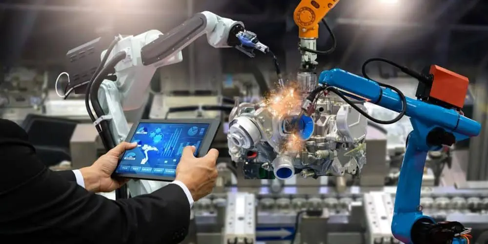
As a leading provider of cost-effective and high-quality PCB fabrication and assembly services, we support over 1000+ engineers in their research and development projects. Every day, we address questions from customers worldwide about our PCB and assembly solutions. To help new customers better understand our products and services, weโ€™ve compiled these frequently asked questions for your reference.

Q1. Who is RayMing PCB?

RayMing PCB is a trusted and professional provider of PCB fabrication and PCBA services. With years of experience in the industry, RayMing specializes in delivering high-quality, cost-effective solutions for a wide range of applications, including consumer electronics, industrial equipment, medical devices, and research projects.
The company is known for its commitment to precision, reliability, and customer satisfaction. RayMing PCB offers comprehensive services, from PCB prototyping to full-scale production, including turnkey assembly, component sourcing, and testing. Their advanced manufacturing facilities, skilled engineering team, and dedication to innovation make them a preferred partner for engineers, businesses, and researchers worldwide.
Whether you’re working on a small prototype or a large-scale production run, RayMing PCB provides tailored solutions to meet your specific needs, ensuring high-quality results and on-time delivery.

Q2. Is there any MOQ requirements for the PCB Assembly order ?

Generally, there is no minimum order quantity (MOQ) requirement for the pcb assembly order.

Q3. Can you assemble boards not manufactured by RayMing?

At this time, we do not offer assembly services for PCBs manufactured by other companies. Our process is designed to provide a seamless and integrated experience, combining PCB fabrication, component sourcing, and assembly under one roof. This approach ensures efficiency, quality control, and cost-effectiveness, ultimately saving our customers time and money. By handling the entire production process internally, we can guarantee consistent results and a smoother workflow for your projects.

Q4. What files and documents are required for my PCBA orders?

For your PCBA orders, we require the following files:ย Gerber files,ย Centroid data, and aย BOM (Bill of Materials). If youโ€™ve already placed your PCB order with us and your Gerber files include the essential layersโ€”silkscreen,ย copper track, andย solder pasteโ€”you only need to provide the Centroid data and BOM.
However, if your Gerber files are missing any of these three critical layers, please resend the updated files, as these are the minimum requirements for assembly.
For the best possible results, we also recommend submitting additional documents such asย assembly drawings,ย special instructions, andย photosย of your project. While these are not mandatory, they help us better understand your requirements, avoid ambiguities, and prevent potential errors in component placement. Providing these details ensures a smoother and more accurate assembly process.

Q5. What is a Centroid File?

A Centroid file is a specialized file used in the assembly process to program automated assembly machines efficiently. It is also referred to asย Insertion,ย Pick-and-Place, orย XY Data. This file provides detailed information about the placement and orientation of all surface-mount components on the PCB.
The Centroid file includes:
Reference Designator
X and Y Coordinatesย (position on the board)
Rotationย (orientation of the component)
Board Sideย (Top or Bottom)
While some CAD tools automatically generate this file, others may require manual adjustments before the Centroid file can be created. Itโ€™s important to note that only surface-mount components are listed in the Centroid file, as it is specifically designed for automated placement of these parts.
Providing an accurate Centroid file ensures precise and efficient assembly of your PCB.

Q6. How should parts be shipped and marked for consigned or kitted orders?

For consigned or kitted orders, we kindly request that you mark each individual package or box with the following details:
Line Numberย (as listed in the BOM)
Manufacturerโ€™s Part Numberย orย Customerโ€™s Part Number
Quantities
Additionally, please include aย detailed packing listย with your shipment. This list will help us efficiently count, verify, and organize the parts upon receipt. Clear labeling and documentation ensure a smooth and accurate assembly process, minimizing delays or errors.

Q7. What are your requirements for parts overages in consigned/kitted PCBA orders?

For consigned or kitted PCBA orders, please note the following guidelines regarding parts overages:
Return of Unused Parts:
Unused or excess parts provided by you or purchased by us will not be returned by default. If you wish to have these parts returned with your assembled boards, please inform your service representative or add a note to your order specifying which parts should be sent back.
Packaging for SMT Parts:
SMT parts not supplied on reels must be provided on one continuous strip of tape.
If the same SMT part is used across multiple boards, do not cut them into strips. Keep them on a continuous strip of tape or on reels.
Minimum and Excess Quantities for Common Components:
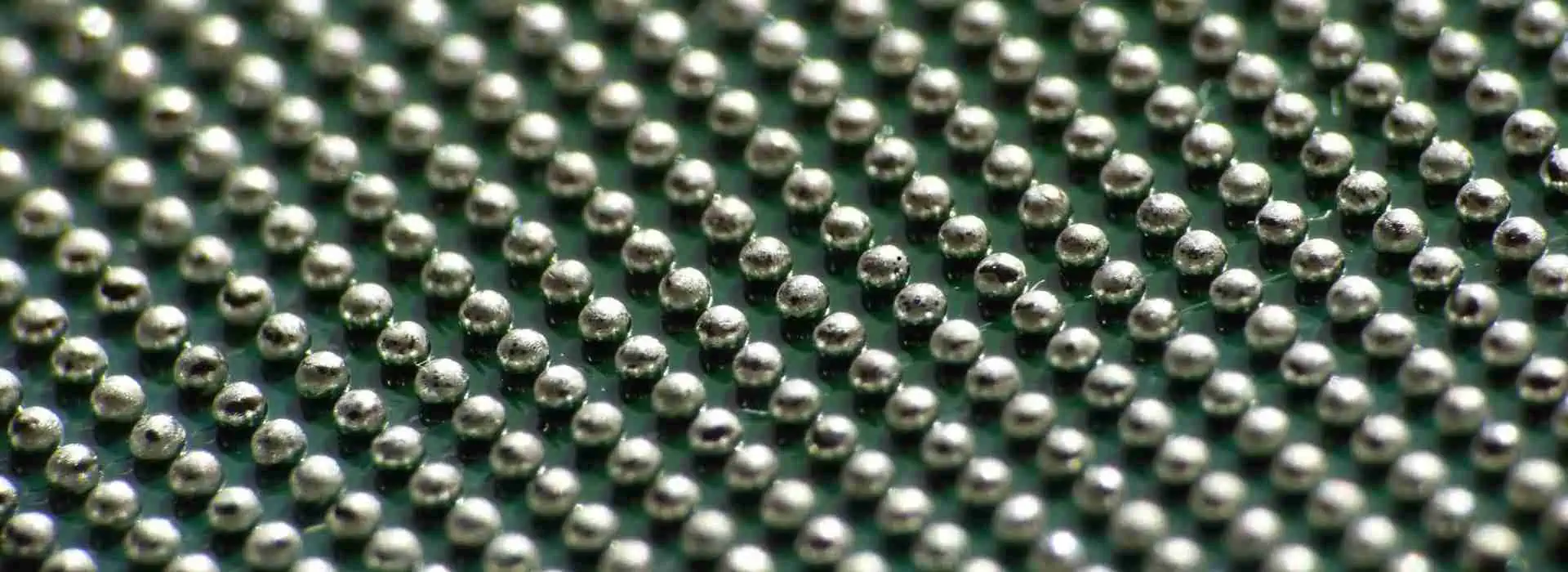
Resistors, Capacitors, Diodesย (0603, 0805, 1206, 2225, SOT, SOD, MELF packages):
Minimum: 50 pieces
Excess: 30 pieces over the required quantity
Example: For an assembly quantity of 40 pieces, provide 70 pieces (50 minimum + 30 excess).
Resistors, Capacitors, Diodesย (0201, 0402, miniMelf, miniature packages):
Minimum: 100 pieces
Excess: 50 pieces over the required quantity
Example: For an assembly quantity of 80 pieces, provide 130 pieces (100 minimum + 50 excess).
Expensive Components (ICs, BGAs, QFPs, Connectors, etc.):
A small excess (1-5 pieces, depending on the total assembly quantity) is recommended to ensure smooth assembly and timely delivery of your boards.
If you are unsure about the quantity, feel free to provide additional extras or contact us for clarification.
Adhering to these guidelines helps us maintain efficiency and ensures your project is completed on time and to the highest standards. If you have any questions, please donโ€™t hesitate to reach out to us.

Q8. Can you source components for my assembly?

Yes, we can! This service is known asย Partial Turn-Key. You have the option to supply some of the components yourself, and we will source the remaining parts on your behalf. During the process, if we encounter any uncertainties regarding part specifications or availability, we will seek your approval before proceeding.
In cases where parts are unavailable or substitutions are required, we will contact you for final confirmation to ensure the selected alternatives meet your requirements. This approach allows us to maintain transparency and ensures your assembly aligns with your expectations.

Q9. Do you assemble BGAs? Are there any special requirements for this?

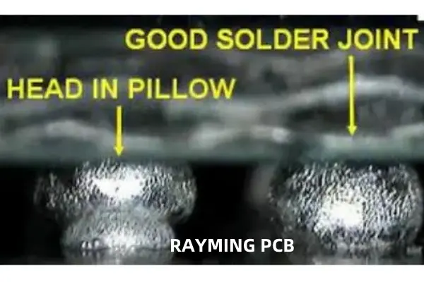
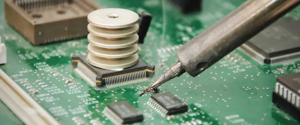
Yes, we are fully equipped to assemble BGAs, including those with a fine pitch ofย 0.25mm, and we provideย X-ray testingย to ensure quality and reliability.
For BGA assembly, there are two common design approaches:ย via on padย andย via near padย (connected by shorter traces). Each design has specific requirements to ensure optimal soldering quality:
Via Near Pad:
Vias located near the BGA pads must beย tented and filled with solder maskย to prevent solder wicking and ensure proper soldering.
Via on Pad:
Vias directly on the BGA pads must beย filled with resinย to create a flat surface, ensuring excellent soldering quality and preventing voids or defects.
By adhering to these guidelines, we guarantee high-quality BGA assembly and reliable performance for your PCBs. If you have any specific requirements or questions, feel free to reach out to us!

Q10. How do you handle excess and unused parts?

Excess parts are common because we typically request a percentage of overage forย consigned/kitted ordersย or purchase additional quantities forย Turn-Key ordersย to ensure smooth assembly. Once your order is complete, you have two options for handling the unused parts:
Ship them back to you: We can return the unused parts along with your assembled boards.
Store them for future use: We can keep the parts in our inventory for your next order.
The choice is entirely yours! Let us know your preference, and weโ€™ll accommodate accordingly.

Q11. How is the total price for PCBA services calculated?

Ourย online instant quote systemย provides a preliminary estimate of the PCBA cost, covering essential elements such asย tooling,ย laser-cut steel stencils, andย labor. Forย Turn-Keyย orย Partial Turn-Key PCBAย services, the cost of components will also be included in the final price. This ensures transparency and helps you understand the breakdown of expenses for your project.

Q12. When does the turnaround time begin?

Determining the turnaround time for PCBA services can be complex due to various factors. As per our policy, theย turnaround time officially beginsย only after the following conditions are met:
All requiredย parts and PCBsย are ready.
All necessary files and documents are submitted, including:
PCB filesย (Gerber files or other formats)
Centroid fileย (Pick & Place/PNP file, XY Data, or equivalent)
BOM (Bill of Materials)
Any additionalย data, documents, images, or photosย essential for the assembly process.
Once all these elements are complete and in place, we initiate the assembly process and the turnaround time starts. This ensures a smooth and efficient workflow for your project.

Q13. Is your assembly RoHS compliant?

Yes, our assembly services areย RoHS compliant, ensuring adherence to environmental and safety standards. However, we also provideย leaded PCBA servicesย for projects that require traditional soldering methods. Let us know your specific requirements, and weโ€™ll accommodate accordingly!

Q14. Why is panelization necessary for my boards?

Panelization is required in the following scenarios:
If your PCB dimensions areย smaller than 50mm x 100mm.
If your PCB has aย non-rectangular shapeย (e.g., circular or irregular).
In such cases, your boards must be arranged in an array (panelized) to facilitate the assembly process. Since we also handle PCB fabrication, once we begin manufacturing your boards, we will generate theย panelization fileย (including solder paste data). This file is then shared with our PCBA department to create a stencil that matches the panelized PCB layout, ensuring precise and efficient assembly. Panelization streamlines production and ensures consistency across your boards.

Q15. Why do I need to design break-away rails (break-away tabs)?

Break-away rails (or tabs) are necessary in the following situations:
If theย clearance between the boardโ€™s edge and copper featuresย is less thanย 3.5mm (138 mil).
If your boards requireย panelizationย for assembly or other reasons.
These rails must be added along theย two longer parallel edgesย of the boards to ensure they can be properly handled and processed by the SMT (Surface Mount Technology) machines. Break-away rails provide structural support during assembly, enabling smooth machine processing and ensuring the boards remain stable throughout the manufacturing process. Once assembly is complete, the rails can be easily removed.

Q16. What should I do if I find defects or issues with the assembled boards after receiving them?

While PCBA is a complex process involving numerous details, defects or issues can occasionally occur. If you encounter any problems, please notify usย immediately. We will thoroughly evaluate and review the situation to determine the best course of action. Depending on the issue, we will eitherย repair/reworkย the boards orย remakeย them entirely.
In some cases, we may request that you return the defective boards to us for further analysis. Rest assured, our goal is to ensure you receiveย fully functional boards, and we stand by our commitment to resolving any issues promptly and effectively. Your satisfaction is our priority!

Q17. What are your PCB Assembly standards?

Our PCB assembly services adhere to theย IPC-A-610 Class 2ย standard. This ensures that your boards meet high-quality reliability and performance criteria, suitable for a wide range of applications where extended product life and uninterrupted service are essential.

Q18. What is the turnaround time for a Turn-Key order?

For Turn-Key orders, the turnaround time primarily depends on the time required toย source all the necessary components. We will keep you updated throughย daily email communicationsย regarding the progress of part sourcing and overall timelines.
While waiting for the parts to arrive, we will proceed withย PCB fabricationย andย stencil preparation. This allows us to begin the assembly process immediately once all components are in hand, ensuring an efficient and streamlined workflow. Rest assured, we prioritize minimizing delays and keeping you informed every step of the way.

Q19. How should I provide special instructions?

You can share your special instructions by either:
Sending us anย emailย detailing your requirements, or
Including aย readme fileย with your specifications when submitting your order.
This ensures we clearly understand your needs and can accommodate any specific requests during the assembly process.

Q20. What types of testing is done on my assembled boards?

a) Visual Inspection b) AOI Inspection c) X-Ray inspection (for BGAโ€™s and fine pitch parts) d) Functional testing (if required by customer)

Q21. Do you provide IC programming and functional testing services?

Yes, we offer both IC programming and functional testing.
For IC programming, we will need the hex file.
For functional testing, please provide the test procedure and the required hardware.

Q22. Do you provide conformal coating services?

Yes, we offer conformal coating services. For further details, feel free to reach out to us at:ย Sales@raypcb.com.

Q23. What factors influence the cost of PCB assembly?

Several key factors directly affect the cost of PCB assembly, such as the technology employed, whether the board is single or double-sided, the number of component placements, coating requirements, testing procedures, shipping needs, and more.

Essential Files for PCBA (Printed Circuit Board Assembly)

To ensure successful completion of your PCBA project, we require specific documentation files that enable accurate and efficient assembly. This guide outlines the mandatory files and recommended documents needed for different order types.

File Submission Guidelines

Submission Methods:

Email Requirements:

  • Subject line format: “Files for Order Number [Your Order Number]”
  • Include all required files as attachments
  • Specify your order type (Consigned, Turn-Key, or Partial Turn-Key)

Required Files

1. Bill of Materials (BOM)

The BOM is a comprehensive inventory of all components needed for your PCB assembly. This critical document ensures we have complete part information for procurement and placement.

Accepted Formats: .xls, .xlsx, or .csv

For Consigned/Kitted Orders

Your BOM must include:

  • Line Number – Sequential numbering for each component
  • Quantity – Number of parts needed per assembly
  • Reference Designator – Component identifier (e.g., R1, C5, U3)
  • Part Number – Your internal part number
  • Description – Clear component description
  • Package TypeSurface Mount, Through-Hole, or Hybrid

For Turn-Key and Partial Turn-Key Orders

Include all above information plus:

  • Manufacturer NameComponent manufacturer
  • Manufacturer Part Number – Official MPN
  • Distributor Part Number – Supplier-specific part number

Download Sample BOM Template

2. Gerber Files

Standard RS-274X format Gerber files identical to those used for PCB fabrication are required for assembly reference.

Minimum Required Layers:

  • Silkscreen Layer – Component outlines and reference designators
  • Copper Layers – All conductive tracks and pads
  • Solder Paste Layer – Stencil data for surface mount components

Important: Thoroughly review all Gerber files before submission. Our team will perform additional verification to ensure completeness and accuracy.

3. Centroid File (Pick and Place Data)

The Centroid file contains precise positioning data for automated assembly equipment. Also known as Insertion, Pick-N-Place, or XY Data file.

Required Information:

  • Reference Designator – Component identifier
  • X/Y Coordinates – Exact placement position
  • Rotation AngleComponent orientation
  • Board Side – Top or Bottom layer placement

Note: This file only includes surface-mount components. Through-hole components are placed manually using assembly drawings and silkscreen references.

Download Sample Centroid Template


Recommended Additional Documentation

While not mandatory, these supplementary documents significantly improve assembly quality and reduce potential errors:

Assembly Drawings

  • Clear visual representation of component placement
  • Special assembly notes and requirements
  • Critical dimension callouts

Special Assembly Instructions

  • Unique handling requirements
  • Component orientation specifications
  • Testing or programming instructions

Reference Images

  • High-resolution photos of assembled PCBs
  • Close-up images of critical areas
  • Before/after assembly comparisons

File Review Process

Your Responsibility:

  • Verify all files are complete and accurate
  • Ensure file formats are compatible
  • Include all required information for your order type

Our Quality Check:

  • Comprehensive file review before assembly begins
  • Cross-reference BOM with Gerber and Centroid data
  • Flag any discrepancies or missing information
  • Communicate with you to resolve issues promptly

Contact Information

File Submissions: Sales@raypcb.com

Questions or Support: Contact our technical team for assistance with file preparation or formatting requirements.

We’re committed to delivering flawless PCBA results and look forward to partnering with you on your project.

A Proposed Mechanism and Remedy for Ball-in-Socket and Foot-in-Mud Soldering Defects on Ball Grid Array and Quad Flat Pack Components

Soldering Balls

Do you involve in electronic PCB board production has probably encountered the phenomenon of “head-in-pillow” defects when soldering BGAs. Here is an interesting technical article describing this type of defect and an effective method to prevent it. 

Powered By EmbedPress

A Proposed Mechanism and Remedy for Ball-in-Socket and Foot-in-Mud Soldering Defects on Ball Grid Array and Quad Flat Pack Components

The miniaturization of electronic components has driven the widespread adoption of advanced packaging technologies such as Ball Grid Array (BGA) and Quad Flat Pack (QFP) components. While these packages offer superior electrical performance and higher pin density, they also introduce unique soldering challenges that can compromise assembly reliability. Among the most concerning defects are the “ball-in-socket” phenomenon affecting BGA components and the “foot-in-mud” defect commonly observed in QFP assemblies. Understanding the underlying mechanisms behind these defects and implementing effective remediation strategies is crucial for maintaining high-quality electronic assemblies.

Understanding Ball-in-Socket Defects in BGA Components

The ball-in-socket defect represents one of the most subtle yet problematic soldering issues in BGA assembly. This defect occurs when the solder ball from the BGA component fails to fully coalesce with the solder paste deposited on the PCB pad, resulting in a hollow cavity or “socket” formation around the solder ball. From external inspection, these joints may appear acceptable, making this defect particularly insidious as it often escapes visual detection while significantly compromising joint reliability.

The formation mechanism of ball-in-socket defects involves several interconnected factors. During the reflow process, the solder paste on the PCB pad begins to melt and wet the surface. Simultaneously, the solder ball attached to the BGA component also reaches its melting point. Under ideal conditions, these two molten solder masses should merge completely, forming a homogeneous joint upon cooling. However, when process parameters are suboptimal, incomplete coalescence occurs.

The primary contributing factors include insufficient reflow temperature profiles that fail to achieve complete solder melting, inadequate dwell time at peak temperature preventing full metallurgical bonding, contamination or oxidation on either the solder ball or PCB pad surface that inhibits proper wetting, and mismatched solder alloy compositions between the ball and paste that create different melting characteristics.

Additionally, the presence of flux residues or volatile compounds that fail to escape during reflow can create gas pockets that prevent complete solder fusion. The surface tension forces between the partially molten solder masses can also contribute to maintaining separation rather than promoting coalescence.

Foot-in-Mud Defects in QFP Components

The foot-in-mud defect affects QFP components and manifests as excessive solder buildup around the component leads, creating an appearance reminiscent of feet stuck in thick mud. This defect is characterized by irregular solder joint geometry with excessive fillet formation that can bridge adjacent pins or create stress concentrations that compromise long-term reliability.

The mechanism behind foot-in-mud formation typically involves excessive solder paste deposition combined with poor solder flow characteristics during reflow. When too much solder paste is applied to the PCB pads, the excess material must flow somewhere during the melting process. In QFP assemblies, this excess solder tends to accumulate around the component leads, particularly in the heel and toe regions of the joint.

Several factors contribute to this defect, including over-application of solder paste due to incorrect stencil design or printing parameters, inadequate component placement force that fails to displace excess paste, improper reflow profile that promotes solder spreading rather than controlled wetting, and flux formulations that provide insufficient surface tension control during the molten phase.

The component’s gull-wing lead design, while beneficial for visual inspection and rework, can exacerbate foot-in-mud formation by creating natural collection points for excess solder. The capillary action between the lead and PCB surface can draw additional molten solder into the joint area, further contributing to the defect formation.

Proposed Remediation Strategies

Addressing these soldering defects requires a comprehensive approach that encompasses process optimization, material selection, and quality control measures. For ball-in-socket defects in BGA assemblies, the primary focus should be on reflow profile optimization. The temperature profile must ensure complete melting of both the solder balls and paste while providing sufficient time above liquidus temperature for complete coalescence.

Implementing a gradual ramp rate during the preheat phase helps minimize thermal shock while ensuring uniform temperature distribution across the assembly. The peak temperature should exceed the solder alloy liquidus point by an appropriate margin, typically 20-30ยฐC for SAC alloys, while maintaining this temperature for 60-90 seconds to ensure complete metallurgical bonding.

Surface preparation plays a crucial role in preventing ball-in-socket formation. Both the BGA component and PCB pads must be free from oxidation, contamination, and flux residues that could inhibit proper wetting. Implementing controlled atmosphere reflow using nitrogen can significantly reduce oxidation and improve solder flow characteristics.

For foot-in-mud defects in QFP assemblies, stencil design optimization is paramount. The aperture size and shape must be carefully calculated to deposit the correct volume of solder paste for each pad size. Implementing area ratio calculations and considering the paste release characteristics can help achieve optimal paste deposition. Typically, maintaining an area ratio between 0.6 and 1.5 provides good paste release while preventing over-deposition.

Component placement parameters also require attention. The placement force should be sufficient to displace excess paste without damaging the component or creating placement accuracy issues. Implementing force feedback during placement can help ensure consistent results across different component types and sizes.

Process Control and Quality Assurance

Effective prevention of these soldering defects requires robust process control and monitoring systems. Statistical process control should be implemented for critical parameters including paste printing thickness and registration, component placement accuracy and force, and reflow temperature profile consistency across the conveyor width.

Advanced inspection techniques such as X-ray imaging can detect ball-in-socket defects that escape visual inspection. Automated X-ray systems can be programmed to identify the characteristic void patterns associated with incomplete solder coalescence, enabling early detection and process correction.

For foot-in-mud defects, automated optical inspection systems can be configured to detect excessive solder buildup and joint geometry irregularities. Implementing measurement algorithms that assess fillet height and width can provide quantitative feedback for process optimization.

Conclusion

Ball-in-socket and foot-in-mud soldering defects represent significant challenges in modern electronic assembly, requiring careful attention to process parameters, material properties, and quality control measures. By understanding the underlying formation mechanisms and implementing comprehensive remediation strategies, manufacturers can achieve reliable, high-quality solder joints that meet the demanding requirements of today’s electronic products. Continuous monitoring and process optimization remain essential for maintaining consistent assembly quality and preventing these subtle but critical defects from compromising product reliability.

Complete Guide to BOM Electronic Components Purchase

HOW TO MAKE BOM

Introduction

A Bill of Materials (BOM) is a comprehensive list of components, materials, and assemblies required to manufacture a product. In the context of electronics, the BOM is a critical document that outlines all the electronic components needed to build a Printed Circuit Board (PCB) or an electronic device. Purchasing electronic components for a BOM can be a complex process, involving careful planning, supplier selection, and quality assurance. This guide provides a complete overview of the BOM electronic components purchase process, from understanding the BOM to sourcing components and managing inventory.


1. Understanding the BOM

1.1 What is a BOM?

A BOM is a detailed list of all the parts and materials required to manufacture a product. In electronics, the BOM includes:

1.2 Types of BOM

There are several types of BOM, each serving a different purpose:

  • Engineering BOM (EBOM):ย Focuses on the design and engineering aspects of the product.

  • Manufacturing BOM (MBOM):ย Includes all the components and materials needed for production.

  • Service BOM (SBOM):ย Lists the parts required for maintenance and repair.

1.3 Importance of an Accurate BOM

An accurate BOM is essential for:

  • Cost Estimation:ย Helps in calculating the total cost of materials.

  • Procurement Planning:ย Ensures that all components are available when needed.

  • Production Efficiency:ย Reduces the risk of delays and errors during manufacturing.

  • Inventory Management:ย Helps in maintaining optimal stock levels.


2. Preparing for Component Purchase

2.1 Reviewing the BOM

Before purchasing components, review the BOM to ensure it is complete and accurate. Check for:

  • Component Specifications:ย Ensure that all components meet the required specifications (e.g., resistance, capacitance, voltage rating).

  • Quantities:ย Verify the quantities needed for each component.

  • Alternate Parts:ย Identify any alternate or substitute components that can be used if the primary part is unavailable.

2.2 Identifying Critical Components

Some components are more critical than others due to their function, availability, or cost. Identify these components early to prioritize their procurement.

2.3 Budgeting

Estimate the total cost of the components based on the BOM. Consider factors such as:

  • Component Costs:ย Unit prices of individual components.

  • Shipping Costs:ย Costs associated with transporting components.

  • Taxes and Duties:ย Import duties and taxes that may apply.


3. Sourcing Electronic Components

3.1 Choosing Suppliers

Selecting the right suppliers is crucial for ensuring the quality and availability of components. Consider the following factors when choosing suppliers:

  • Reputation:ย Look for suppliers with a good reputation for quality and reliability.

  • Lead Times:ย Ensure that the supplier can deliver components within the required timeframe.

  • Minimum Order Quantities (MOQs):ย Check if the supplier has MOQs that align with your needs.

  • Certifications:ย Verify that the supplier has relevant certifications (e.g., ISO 9001).

3.2 Types of Suppliers

There are several types of suppliers to consider:

  • Manufacturers:ย Directly produce the components.

  • Distributors:ย Authorized resellers of components from manufacturers.

  • Brokers:ย Intermediaries who source components from various suppliers.

  • Online Marketplaces:ย Platforms like Digi-Key, Mouser, and Arrow that offer a wide range of components.

3.3 Requesting Quotes

Request quotes from multiple suppliers to compare prices and terms. Provide the following information in your request:

  • Component Part Numbers:ย Ensure that the part numbers match the BOM.

  • Quantities:ย Specify the quantities needed for each component.

  • Delivery Requirements:ย Indicate the required delivery date and location.

3.4 Evaluating Quotes

When evaluating quotes, consider:

  • Price:ย Compare the total cost, including shipping and taxes.

  • Lead Time:ย Ensure that the supplier can meet your delivery requirements.

  • Terms and Conditions:ย Review payment terms, return policies, and warranties.


4. Placing Ordersbom bill of material

4.1 Order Confirmation

Once you have selected a supplier, confirm the order by providing:

  • Purchase Order (PO):ย A formal document outlining the order details.

  • Shipping Information:ย Delivery address and contact information.

  • Payment Details:ย Payment method and terms.

4.2 Tracking Orders

Track the status of your orders to ensure timely delivery. Most suppliers provide tracking information that allows you to monitor the progress of your shipment.

4.3 Receiving and Inspecting Components

Upon receiving the components, inspect them to ensure they meet the required specifications. Check for:

  • Correct Part Numbers:ย Verify that the received components match the part numbers in the BOM.

  • Quantity:ย Ensure that the correct quantity has been delivered.

  • Quality:ย Inspect for any physical damage or defects.


5. Managing Inventory

5.1 Inventory Tracking

Maintain an inventory tracking system to monitor stock levels and usage. This can be done using:

  • Spreadsheets:ย Simple and cost-effective for small-scale operations.

  • Inventory Management Software:ย More advanced solutions that offer real-time tracking and reporting.

5.2 Reordering Components

Set up a reordering system to ensure that you never run out of critical components. Consider:

  • Reorder Points:ย The stock level at which you need to place a new order.

  • Safety Stock:ย A buffer stock to account for variability in demand and lead times.

5.3 Managing Obsolete Components

Electronic components can become obsolete due to technological advancements or changes in market demand. To manage obsolete components:

  • Identify Obsolete Parts:ย Regularly review your BOM for components that are no longer available.

  • Source Alternatives:ย Find alternate parts or redesign the circuit to use available components.

  • Stockpile Critical Parts:ย If possible, stockpile critical components that are at risk of becoming obsolete.


6. Quality Assurance

6.1 Component Testing

Test components to ensure they meet the required specifications. Common tests include:

  • Electrical Testing:ย Verify electrical properties such as resistance, capacitance, and voltage rating.

  • Functional Testing:ย Test the component in a real-world application to ensure it performs as expected.

6.2 Supplier Audits

Conduct regular audits of your suppliers to ensure they maintain high-quality standards. Audits can include:

  • Factory Visits:ย Inspect the supplier’s manufacturing facilities.

  • Quality Certifications:ย Verify that the supplier holds relevant quality certifications.

  • Performance Reviews:ย Assess the supplier’s performance based on delivery times, defect rates, and customer service.

6.3 Handling Defective Components

If you receive defective components, follow these steps:

  • Document the Issue:ย Record details of the defect, including part numbers, quantities, and photos.

  • Contact the Supplier:ย Notify the supplier and request a replacement or refund.

  • Update Inventory:ย Remove defective components from your inventory to prevent them from being used in production.


7. Cost Management

7.1 Negotiating Prices

Negotiate with suppliers to get the best possible prices. Consider:

  • Volume Discounts:ย Request discounts for large orders.

  • Long-Term Contracts:ย Commit to long-term contracts in exchange for lower prices.

  • Bundling:ย Combine multiple orders to reduce shipping costs.

7.2 Reducing Costs

Implement strategies to reduce the overall cost of components:

  • Design for Manufacturability (DFM):ย Optimize the design to use standard, readily available components.

  • Value Engineering:ย Identify and eliminate unnecessary costs without compromising quality.

  • Bulk Purchasing:ย Purchase components in bulk to take advantage of volume discounts.


Conclusion

Purchasing electronic components for a BOM is a critical process that requires careful planning, supplier selection, and quality assurance. By understanding the BOM, sourcing components from reliable suppliers, and managing inventory effectively, you can ensure the successful production of your electronic devices. Additionally, implementing cost management strategies and maintaining high-quality standards will help you achieve a competitive edge in the market. Whether you are a hobbyist or a professional, this guide provides the essential knowledge and tools to navigate the complex world of BOM electronic components purchase.

Complete Guide to Programmable IC Marking Procedures

Introduction

Programmable integrated circuits (ICs) like Field-Programmable Gate Arrays (FPGAs), Complex Programmable Logic Devices (CPLDs), and microcontrollers require precise identification through standardized markings. These markings are essential for proper identification, supply chain traceability, regulatory compliance, and preventing counterfeiting.

This comprehensive guide provides engineers and manufacturers with a structured approach to defining effective IC marking procedures that balance technical requirements, regulatory compliance, and operational efficiency.

YouTube video

What is Programmable IC Marking?

Programmable IC marking consists of alphanumeric codes, symbols, logos, and identifiers that are printed or laser-etched directly onto the IC surface. These markings serve multiple critical functions:

  • Product identification through unique part numbers and manufacturer details
  • Supply chain traceability for quality control and recall management
  • Regulatory compliance with international standards like RoHS, CE, and UL
  • Brand protection through manufacturer logos and anti-counterfeiting features
  • Programming status indicating whether the IC is blank or pre-programmed

Essential Elements of IC Markings

Core Information Requirements

Part Number: The unique model identifier (e.g., XC7A35T-1CPG236C for Xilinx FPGAs) that specifies the exact IC variant and capabilities.

Manufacturer Identity: Company name or logo for brand recognition and authenticity verification.

Date Code: Manufacturing date in standard format (e.g., 2125 for week 25 of 2021) enabling age tracking and warranty management.

Lot/Batch Code: Production batch identifier crucial for traceability and quality control investigations.

Country of Origin: Required for customs compliance and international trade regulations.

Additional Marking Elements

Regulatory Symbols: Compliance marks such as RoHS, CE, FCC, or AEC-Q100 for automotive applications.

Programming Information: Status indicators like “Blank,” “Pre-Programmed,” or firmware version numbers.

Security Features: Anti-counterfeiting elements including unique serial numbers, QR codes, or holographic elements.

YouTube video

Step-by-Step Marking Procedure

Phase 1: Requirements Analysis

Regulatory Research Begin by identifying all mandatory markings for your target markets. European markets require CE marking, while China mandates CCC marks for certain products. Environmental regulations like RoHS must be clearly indicated on compliant devices.

Industry Standard Compliance Follow established standards such as JEDEC JESD22-B111 for moisture sensitivity requirements and IPC-7351 for component labeling guidelines. Military and aerospace applications require adherence to MIL-STD-883 or AS9100 standards.

Phase 2: Content Definition

Mandatory Information Framework Establish the core elements that must appear on every IC: part number, manufacturer identification, manufacturing date, and country of origin. These elements form the foundation of your marking system.

Optional Enhancement Features Consider adding firmware version numbers, programming status indicators, or application-specific text like “For Industrial Use Only.” These additions provide valuable information for end-users and system integrators.

Security Integration Implement anti-counterfeiting measures through QR codes linked to authentication databases or laser-etched serial numbers that are difficult to replicate.

Phase 3: Layout Design

Spatial Optimization Design markings to fit within available IC surface area, typically 3ร—3 mm for compact packages. Avoid placement near wire bonding pads, thermal vias, or heat-sensitive regions that could affect IC performance.

Typography Selection Use clear, legible fonts such as sans-serif typefaces (Arial recommended) with minimum heights of 0.5 mm for laser etching and 1.0 mm for ink printing to ensure readability under magnification.

Visual Hierarchy Arrange information by importance, placing critical identifiers like part numbers in prominent positions while organizing secondary information logically around the primary markings.

Phase 4: Technology Selection

Laser Marking Systems Ideal for permanent, high-precision applications with excellent durability. Best suited for ceramic or plastic packages (QFP, BGA). While initial equipment costs are high, operating costs are low with no consumables required.

Inkjet Printing Cost-effective solution for high-volume production with lower equipment investment. Suitable for consumer electronics where absolute permanence isn’t critical. Consider environmental protection for outdoor or harsh-environment applications.

Chemical Etching Provides deep, tamper-proof markings primarily for metal-can packages. Offers excellent durability but is limited in package compatibility and design flexibility.

Phase 5: Quality Validation

Automated Inspection Implement Automated Optical Inspection (AOI) systems using machine vision to verify marking alignment, contrast ratios, and character legibility. Establish minimum contrast thresholds (typically 30% for laser marks).

Environmental Durability Testing Subject marked samples to accelerated aging tests including humidity exposure, temperature cycling (-40ยฐC to 125ยฐC), and UV radiation to verify marking permanence under operational conditions.

Human Readability Assessment Conduct systematic readability tests using standard magnification tools to ensure markings remain legible throughout the product lifecycle.

Phase 6: Traceability Implementation

Database Integration Develop centralized tracking systems linking lot codes and serial numbers to production records, enabling real-time supply chain visibility and rapid response to quality issues.

Digital Code Integration Implement 2D barcodes or QR codes encoding essential product information for rapid scanning and automated data capture throughout manufacturing and distribution processes.

Phase 7: Documentation and Training

Specification Documentation Create comprehensive marking specification documents detailing approved fonts, sizes, placement coordinates, contrast requirements, and inspection criteria. Include visual examples and tolerance specifications.

Personnel Training Conduct thorough training programs for production staff, quality inspectors, and suppliers to ensure consistent implementation and proper handling procedures.

Phase 8: Continuous Improvement

Regular Auditing Establish periodic review cycles to assess marking quality, compliance status, and effectiveness. Update procedures to reflect regulatory changes or design improvements.

Feedback Integration Collect input from field engineers, customers, and supply chain partners to identify improvement opportunities and address practical challenges.

Common Challenges and Solutions

Space Limitations

Challenge: Miniaturized packages like WLCSP provide minimal marking area. Solution: Develop standardized abbreviation systems and prioritize critical information. Consider alternative marking locations on package substrates.

Cost vs. Durability Trade-offs

Challenge: Balancing marking permanence with production economics. Solution: Apply risk-based marking strategies, using premium methods for high-reliability applications while optimizing costs for commercial products.

Counterfeiting Prevention

Challenge: Sophisticated counterfeiters can replicate standard markings. Solution: Implement multi-layer security including cryptographic QR codes, holographic elements, and database verification systems.

Industry Best Practices

Standardization Across Product Lines Maintain consistent formatting conventions for part numbers, date codes, and layout structures to reduce confusion and streamline manufacturing processes.

Critical Information Prioritization Position the most important identifiers (part numbers, lot codes) in the most visible and protected locations on the IC package.

Process Automation Leverage automated inspection systems to minimize human error, increase throughput, and maintain consistent quality standards.

Early Validation Test marking procedures during prototyping phases to identify and resolve issues before full production implementation.

Case Study: Automotive FPGA Marking

Project Requirements

An automotive supplier needed compliant markings for engine control unit FPGAs meeting AEC-Q100 automotive standards with enhanced durability for harsh operating environments.

Implementation Strategy

The team selected laser marking on ceramic packages, incorporating part numbers, date codes, AEC-Q100 compliance logos, and QR codes for complete traceability.

Validation Process

Extensive testing included thermal cycling (-40ยฐC to 125ยฐC), vibration testing, and salt spray exposure to verify marking durability under automotive operating conditions.

Results

The implementation achieved full regulatory compliance with durable, traceable markings that maintained legibility throughout accelerated life testing equivalent to 15 years of automotive operation.

Future Technology Trends

Smart Marking Systems

Emerging technologies include embedded RFID tags and NFC-enabled codes providing real-time tracking capabilities and enhanced authentication features.

AI-Enhanced Inspection

Machine learning algorithms are being developed to detect subtle counterfeiting attempts and automatically adjust inspection parameters for optimal quality control.

Sustainable Marking Solutions

Environmental considerations are driving development of eco-friendly marking inks, energy-efficient laser systems, and biodegradable security features.

Conclusion

Successfully defining programmable IC marking procedures requires systematic planning, cross-functional collaboration, and careful attention to regulatory requirements. By following structured implementation phases and incorporating industry best practices, manufacturers can develop marking systems that enhance product identification, ensure compliance, and protect against counterfeiting while optimizing production efficiency.

The continued evolution of programmable ICs demands ongoing adaptation of marking procedures to address new technologies, regulatory changes, and security challenges. Organizations that invest in robust marking systems will benefit from improved supply chain visibility, enhanced product authentication, and stronger customer confidence in their products.


Frequently Asked Questions (FAQs)

General Questions

Q: What is the difference between programmable and non-programmable IC marking? A: Programmable IC markings often include additional information such as programming status (blank or pre-programmed), firmware version numbers, and security features for field updates. Non-programmable ICs typically only require basic identification markings like part numbers and manufacturing details.

Q: How long do IC markings need to remain legible? A: Marking durability requirements vary by application. Consumer electronics typically require 5-10 years of legibility, while automotive and industrial applications may require 15-25 years. Military and aerospace applications often require markings to last the entire operational lifetime, which can exceed 30 years.

Q: Are there international standards for IC marking? A: Yes, key standards include JEDEC JESD22-B111 for moisture sensitivity markings, IPC-7351 for component labeling, and ISO/IEC 80079 for explosive atmosphere equipment. Regional requirements include CE marking for Europe and CCC marking for China.

Technical Questions

Q: What is the minimum font size for IC markings? A: Minimum font heights are typically 0.5 mm for laser etching and 1.0 mm for ink printing. However, this may vary based on package size, marking technology, and readability requirements. Some miniaturized packages may require smaller fonts with enhanced contrast.

Q: Can QR codes be used on small IC packages? A: Yes, QR codes can be miniaturized to fit on IC packages as small as 3ร—3 mm. High-resolution laser marking systems can create readable QR codes containing basic product information, though data capacity is limited by size constraints.

Q: How do you prevent thermal damage during laser marking? A: Use pulsed laser systems with controlled power settings, optimize marking speed to minimize heat buildup, and select appropriate wavelengths for the package material. Conduct thermal analysis during process development to establish safe operating parameters.

Compliance and Quality Questions

Q: What happens if IC markings don’t meet regulatory requirements? A: Non-compliant markings can result in customs delays, market access restrictions, product recalls, and regulatory penalties. In severe cases, products may be banned from certain markets until compliance is achieved.

Q: How often should marking quality be inspected? A: Implement statistical process control with sampling rates based on production volume and criticality. Typical inspection frequencies range from 100% for aerospace applications to statistical sampling (e.g., 1 in 100) for commercial products.

Q: What anti-counterfeiting measures are most effective for ICs? A: Multi-layer approaches work best, combining physical security features (laser-etched serial numbers), digital authentication (encrypted QR codes), and database verification systems. No single method is foolproof, but layered security significantly increases counterfeiting difficulty.

Production and Cost Questions

Q: What’s the cost difference between marking technologies? A: Laser marking has higher equipment costs ($50,000-$200,000) but lower per-unit costs and no consumables. Inkjet systems cost less initially ($10,000-$50,000) but require ongoing ink and maintenance expenses. Choose based on production volume and durability requirements.

Q: Can existing production lines be retrofitted with marking systems? A: Yes, most marking systems can be integrated into existing production lines. Consider factors like line speed, package handling requirements, and available space. Modular marking systems offer flexibility for retrofit applications.

Q: How do you handle marking for different package types in the same product family? A: Develop scalable marking templates that adapt to different package sizes while maintaining consistent information hierarchy. Use standardized abbreviations and symbols that work across all package variants to maintain brand consistency and reduce training requirements.

PCB Chip Package Soldering Method and Process Flow

Printed Circuit Board (PCB) chip package soldering is a critical process in electronic manufacturing that demands precision, technical expertise, and a thorough understanding of various soldering techniques. This comprehensive guide will explore the intricate world of chip package soldering, providing detailed insights into methods, processes, and best practices.

YouTube video

Understanding Chip Packages

Types of Chip Packages

Package TypeCharacteristicsCommon Applications
DIP (Dual In-line Package)Through-hole mountingOlder electronics, prototyping
QFP (Quad Flat Package)Surface mountMicrocontrollers, processors
BGA (Ball Grid Array)High-density interconnectionAdvanced computing, telecommunications
SOIC (Small Outline Integrated Circuit)Compact surface mountGeneral electronic devices

Package Selection Considerations

  1. Electrical Requirements
  2. Mechanical Constraints
    • Board space
    • Thermal management
    • Mechanical stress tolerance

Soldering Methods

Soldering Circuit Boards

Surface Mount Technology (SMT)

Reflow Soldering Process

StageTemperature RangePrimary Purpose
Preheat100-150ยฐCRemove moisture
Soak150-180ยฐCActivate flux
Reflow217-250ยฐCMelt solder
Cooling50-100ยฐCSolidify connection

Through-Hole Soldering

Manual Soldering Techniques

  1. Hand Soldering Process
    • Use temperature-controlled soldering iron
    • Select appropriate tip size
    • Apply minimal heat duration
  2. Specialized Techniques

Advanced Soldering Technologies

Specialized Soldering Methods

  1. Vapor Phase Soldering
    • Uniform heating
    • Minimized thermal stress
    • Ideal for complex packages
  2. Laser Soldering
    • Precise heat application
    • Minimal thermal impact
    • Suitable for sensitive components

Preparation and Pre-Soldering Considerations

Workspace Setup

Essential ElementRecommended Specification
Workspace Temperature20-25ยฐC
Humidity Control40-60% relative humidity
LightingBright, even illumination
Anti-Static ProtectionGrounded workspace

Component Handling Protocols

  1. Electrostatic Discharge (ESD) Protection
    • Use grounded wrist straps
    • Implement static-free environments
    • Handle components with care
  2. Component Storage
    • Controlled temperature
    • Moisture-barrier packaging
    • Proper labeling and tracking

Soldering Process Flow

SMT-Through-Hole-Soldering

Comprehensive Soldering Workflow

  1. Pre-Soldering Preparation
    • Inspect PCB and components
    • Clean surfaces
    • Apply flux if necessary
  2. Alignment and Placement
    • Precise component positioning
    • Verify orientation
    • Minimal mechanical stress
  3. Soldering Execution
    • Control temperature
    • Minimize contact time
    • Ensure complete solder coverage
  4. Post-Soldering Inspection
    • Visual examination
    • Electrical testing
    • Thermal imaging (optional)

Defect Detection and Prevention

Common Soldering Defects

Defect TypeCharacteristicsPrevention Strategy
Solder BridgingUnintended connectionsPrecise paste application
Cold JointsWeak electrical connectionProper temperature control
TombstoningComponent liftingBalanced thermal profile
VoidingInternal solder gapsOptimize reflow parameters

Inspection Techniques

  1. Visual Inspection
    • Magnification
    • Lighting conditions
    • Standardized evaluation criteria
  2. Advanced Testing
    • X-ray inspection
    • Automated optical inspection (AOI)
    • Electrical performance testing

Thermal Management

Heat-Related Considerations

  1. Thermal Profiling
    • Create precise temperature curve
    • Account for component sensitivity
    • Minimize thermal stress
  2. Cooling Strategies
    • Controlled cooling rates
    • Minimize thermal shock
    • Implement heat sinks if required

Specialized Techniques for Complex Packages

Challenging Package Types

  1. BGA Soldering Challenges
    • Invisible connections
    • Precise alignment
    • X-ray verification techniques
  2. Miniaturization Considerations
    • Micro-soldering techniques
    • Advanced optical alignment
    • Precision equipment

Emerging Soldering Technologies

Future Trends

  1. Environmentally Friendly Processes
    • Lead-free soldering
    • Reduced chemical usage
    • Sustainable manufacturing
  2. Automation and Precision
    • Machine learning integration
    • Robotic soldering systems
    • Advanced process control

Frequently Asked Questions (FAQ)

Q1: What is the most critical factor in successful chip package soldering?

A: Precise temperature control and proper flux application are crucial. Consistent, controlled heat and clean surfaces ensure reliable solder joints.

Q2: How do I choose between different soldering methods?

A: Consider package type, component sensitivity, production volume, and available equipment. Each method has specific advantages for different scenarios.

Q3: What are the main challenges with BGA package soldering?

A: BGA packages have hidden connections, requiring advanced alignment techniques, X-ray inspection, and precise temperature profiling.

Q4: How can I minimize soldering defects?

A: Implement strict process controls, use high-quality materials, maintain clean work environments, and invest in proper training and equipment.

Q5: Are lead-free soldering techniques really necessary?

A: Yes, lead-free soldering is increasingly important due to environmental regulations and health considerations. Modern techniques have significantly improved reliability.

Conclusion

PCB chip package soldering represents a complex intersection of technical skill, scientific precision, and technological innovation. Mastering these techniques requires continuous learning, attention to detail, and a commitment to quality.

As electronic devices become increasingly sophisticated, soldering techniques will continue to evolve, demanding adaptability, expertise, and a deep understanding of emerging technologies.

Microcontroller Tutorial 5/5: Soldering and Programming the Circuit

pic programming Vs. microcontroller programming

In this final installment of our microcontroller tutorial series, we will delve into the practical aspects of bringing your microcontroller-based project to life: soldering and programming the circuit. By this stage, you should have a solid understanding of microcontroller basics, circuit design, and component selection. Now, itโ€™s time to assemble your circuit and program the microcontroller to perform its intended functions. This tutorial will guide you through the soldering process, programming techniques, and troubleshooting tips to ensure your project is successful.

YouTube video

1. Introduction to Soldering

Soldering is the process of joining two or more electronic components together using a filler metal called solder. It is a fundamental skill in electronics, enabling you to create permanent and reliable connections between components and a printed circuit board (PCB). Proper soldering ensures that your circuit functions as intended and minimizes the risk of loose connections or short circuits.

1.1 Tools and Materials Needed

Before you begin soldering, gather the following tools and materials:

  • Soldering Iron: A temperature-controlled soldering iron is ideal for precision work.
  • Solder: Use rosin-core solder with a diameter of 0.8mm or 1mm for general-purpose soldering.
  • Flux: Flux helps improve the flow of solder and ensures clean connections.
  • Soldering Stand: Keeps the soldering iron safe when not in use.
  • Sponge or Brass Wool: For cleaning the soldering iron tip.
  • Desoldering Pump or Braid: For correcting mistakes or removing components.
  • PCB and Components: Your designed circuit board and the necessary components.
  • Safety Gear: Safety glasses and a well-ventilated workspace.

1.2 Soldering Techniques

Hereโ€™s a step-by-step guide to soldering your circuit:

  1. Prepare the Soldering Iron: Heat the soldering iron to the appropriate temperature (typically 300-350ยฐC). Clean the tip using a damp sponge or brass wool.
  2. Position the Components: Insert the components into their designated holes on the PCB. Ensure they are flush against the board and properly aligned.
  3. Apply Heat and Solder: Touch the soldering iron tip to the component lead and PCB pad simultaneously. After a second, feed a small amount of solder onto the joint. The solder should flow smoothly and form a shiny, cone-shaped joint.
  4. Inspect the Joint: A good solder joint should be smooth, shiny, and free of cracks or voids. If the joint looks dull or lumpy, reheat it and add a bit more solder.
  5. Trim Excess Leads: Use wire cutters to trim any excess component leads close to the solder joint.

1.3 Common Soldering Mistakes

  • Cold Joints: Occur when the solder doesnโ€™t melt completely, resulting in a weak connection. Reheat the joint and add fresh solder.
  • Bridging: Happens when solder accidentally connects two adjacent pins or pads. Use desoldering braid to remove excess solder.
  • Overheating: Excessive heat can damage components or lift PCB pads. Work quickly and avoid prolonged contact with the soldering iron.

2. Assembling the Circuit

Once youโ€™ve soldered all the components onto the PCB, itโ€™s time to assemble the circuit. Follow these steps:

  1. Double-Check Connections: Use a multimeter to verify continuity and ensure there are no short circuits or open connections.
  2. Secure the PCB: Mount the PCB in its enclosure or on a stable surface to prevent movement during testing.
  3. Connect Power: Attach the power supply to the circuit, ensuring the voltage matches the microcontrollerโ€™s requirements.
  4. Test Basic Functionality: Before programming, verify that the circuit powers up without issues (e.g., no smoke or overheating).

3. Programming the Microcontroller

Programming is the process of uploading code to the microcontroller, enabling it to perform specific tasks. The exact steps depend on the microcontroller youโ€™re using (e.g., Arduino, PIC, STM32), but the general process is similar.

3.1 Tools and Software

  • Development Board (Optional): Some microcontrollers, like the Arduino, can be programmed using a development board.
  • Programmer/Debugger: Devices like the AVR ISP, ST-Link, or PICkit are used to upload code to the microcontroller.
  • IDE (Integrated Development Environment): Software like Arduino IDE, MPLAB X, or STM32CubeIDE for writing and compiling code.
  • USB Cable: For connecting the microcontroller to your computer.

3.2 Writing the Code

  1. Open the IDE: Launch the appropriate IDE for your microcontroller.
  2. Create a New Project: Set up a new project and select the correct microcontroller model.
  3. Write the Code: Use C, C++, or another supported language to write your program. Include necessary libraries and define pin configurations.
  4. Compile the Code: Check for errors and compile the code into a binary file (hex file) that the microcontroller can execute.

3.3 Uploading the Code

  1. Connect the Microcontroller: Use a programmer/debugger or USB cable to connect the microcontroller to your computer.
  2. Select the Programmer: In the IDE, choose the correct programmer and communication port.
  3. Upload the Code: Click the โ€œUploadโ€ button to transfer the compiled code to the microcontroller.
  4. Verify the Upload: The IDE will display a success message if the upload is complete. If thereโ€™s an error, check the connections and settings.

3.4 Debugging and Testing

  • Serial Monitor: Use the serial monitor in the IDE to view debug messages and monitor the programโ€™s behavior.
  • LED Indicators: Add LEDs to the circuit to visually confirm the programโ€™s execution.
  • Multimeter and Oscilloscope: Measure voltages and signals to ensure the circuit is functioning as expected.

4. Troubleshooting Common Issues

Even with careful assembly and programming, issues can arise. Here are some common problems and their solutions:

  1. Circuit Doesnโ€™t Power On:
    • Check the power supply connections and voltage.
    • Verify that the polarity of components like capacitors and diodes is correct.
  2. Code Doesnโ€™t Upload:
    • Ensure the programmer is properly connected and recognized by the IDE.
    • Verify that the correct microcontroller model and communication settings are selected.
  3. Unexpected Behavior:
    • Review the code for logical errors or incorrect pin assignments.
    • Check for loose connections or faulty components.
  4. Overheating Components:
    • Disconnect power immediately and inspect for short circuits or incorrect component values.

5. Best Practices for Soldering and Programming

To ensure a successful project, follow these best practices:

  • Work in a Clean, Organized Space: Keep your workspace tidy to avoid losing components or making mistakes.
  • Use Quality Tools: Invest in a good soldering iron, solder, and other tools for reliable results.
  • Follow Datasheets: Refer to the datasheets for your microcontroller and components to ensure proper usage.
  • Test Incrementally: Test each part of the circuit as you build it to catch issues early.
  • Document Your Work: Keep a record of your circuit design, code, and any changes you make for future reference.

6. Expanding Your Project

Once your circuit is soldered and programmed, you can expand its functionality by:

  • Adding Sensors: Integrate sensors like temperature, motion, or light sensors to gather data.
  • Connecting to Displays: Use LCDs or OLEDs to display information.
  • Implementing Communication: Add modules for Wi-Fi, Bluetooth, or serial communication to enable remote control or data transfer.
  • Enhancing Power Management: Incorporate battery packs or solar panels for portable or off-grid applications.

7. Conclusion

Soldering and programming are the final steps in bringing your microcontroller project to life. By mastering these skills, you can create reliable, functional circuits that perform a wide range of tasks. Remember to take your time, follow best practices, and donโ€™t be afraid to experiment and learn from mistakes. With practice, youโ€™ll gain confidence and be able to tackle more complex projects in the future.

This concludes our five-part microcontroller tutorial series. We hope these guides have provided you with a solid foundation in microcontroller basics, circuit design, component selection, and practical implementation. Happy building!

How to Program FPGA by Yourself: A Complete Guide

Field-Programmable Gate Arrays (FPGAs) are semiconductor devices consisting of configurable logic blocks connected through programmable interconnects. Unlike microprocessors that execute sequential instructions, FPGAs can implement any digital logic function through parallel processing, making them incredibly versatile for various applications.

YouTube video

Key FPGA Components

ComponentDescriptionPurpose
Logic Elements (LEs)Basic building blocksImplement combinational and sequential logic
Look-Up Tables (LUTs)Truth table implementationDefine logic functions
Flip-FlopsStorage elementsStore binary states
I/O BlocksInterface componentsConnect FPGA to external devices
Clock NetworksSignal distributionSynchronize operations
Memory BlocksStorage arraysStore data and instructions

Getting Started with FPGA Programming

Essential Tools and Software

CategoryRequired ToolsPurpose
Hardware Description LanguageVHDL/Verilog EditorCode development
Synthesis ToolVendor-specific (e.g., Vivado, Quartus)Convert HDL to netlist
Simulation SoftwareModelSim, GHDLVerify design behavior
Programming CableUSB Blaster, JTAGDownload design to FPGA
Development BoardStarter kitHardware platform

Choosing Your First FPGA

ManufacturerEntry-Level BoardFeaturesBest For
XilinxArtix-7Moderate resources, good docsGeneral learning
Intel (Altera)Cyclone IVCost-effective, simpleBeginners
LatticeiCE40Ultra-low power, compactSimple projects

HDL Programming Fundamentals

VHDL vs. Verilog Comparison

AspectVHDLVerilog
OriginMilitary/AerospaceCommercial/Industry
SyntaxAda-like, verboseC-like, concise
Type SystemStrongly typedLoosely typed
Learning CurveSteeperModerate
Debug CapabilityBetterGood

Basic HDL Concepts

Common HDL Structures

StructurePurposeExample Usage
Entity/ModuleDefine interfacePort declarations
Architecture/ImplementationDescribe behaviorLogic implementation
Process/AlwaysSequential logicState machines
Concurrent StatementsCombinational logicDirect assignments

Design Methodology

Design Flow Steps

  1. Specification
  2. HDL Coding
  3. Simulation
  4. Synthesis
  5. Implementation
  6. Timing Analysis
  7. Programming
  8. Verification

Design Best Practices

Coding Guidelines

AspectRecommendationReason
Clock DomainsMinimize numberReduce complexity
SynchronizationUse proper techniquesPrevent metastability
Resource UsageMonitor utilizationOptimize performance
DocumentationComment thoroughlyMaintain code

Advanced FPGA Concepts

Memory Types and Usage

Memory TypeCharacteristicsBest Use Case
Distributed RAMFast, small capacityLocal storage
Block RAMLarger, dedicatedData buffers
Shift RegistersSequential accessFIFO, delays
External MemoryHighest capacityMass storage

Clock Management

Clock Domain Considerations

AspectImplementationPurpose
PLL/DLLClock multiplication/divisionFrequency synthesis
Clock GatingEnable/disable clocksPower management
Clock CrossingSynchronization circuitsMulti-domain designs

Implementation Techniques

ic programming services

State Machine Design

TypeCharacteristicsBest For
MealyOutput depends on inputsProtocol handling
MooreOutput depends on statePredictable timing
HybridCombines bothComplex control

Common Design Patterns

PatternUse CaseBenefits
PipelineData processingHigher throughput
FIFOData bufferingClock domain crossing
ArbiterResource sharingMulti-master systems

Debugging and Verification

Simulation Strategies

LevelPurposeTools
BehavioralFunctional verificationHDL simulator
Post-synthesisLogic verificationVendor tools
Post-implementationTiming verificationTiming analyzer

Debug Tools

Tool TypeFeaturesApplication
Logic AnalyzerSignal captureRuntime debug
ChipScope/SignalTapInternal probingDeep debug
JTAGBoundary scanBoard test

Project Examples

Beginner Projects

ProjectComplexitySkills Learned
LED ControllerLowBasic I/O, counters
UART InterfaceMediumSerial protocols
Simple ALUMediumCombinational logic
VGA ControllerHighTiming, memory

Frequently Asked Questions

Q1: How long does it take to learn FPGA programming?

A: Learning FPGA programming typically takes 3-6 months to grasp the basics and 1-2 years to become proficient. The learning curve depends on:

  • Prior digital design experience
  • Programming background
  • Time commitment
  • Project complexity level

Q2: Which HDL should I learn first – VHDL or Verilog?

A: For beginners, Verilog is often recommended because:

  • More C-like syntax feels familiar to software developers
  • Less verbose than VHDL
  • Widely used in industry
  • More flexible for small projects However, both languages are equally capable, and the choice often depends on your region and industry.

Q3: What are the common mistakes beginners make in FPGA design?

A: Common beginner mistakes include:

  • Thinking in software terms instead of hardware
  • Improper clock domain crossing
  • Inadequate timing constraints
  • Not considering hardware resources
  • Insufficient simulation testing

Q4: What computer specifications are needed for FPGA development?

A: Recommended specifications:

  • Processor: Modern multi-core CPU (i5/i7 or equivalent)
  • RAM: Minimum 16GB, 32GB recommended
  • Storage: 256GB+ SSD
  • OS: Windows 10/11 or Linux
  • Multiple monitors recommended

Q5: How do I choose the right FPGA for my project?

A: Consider these factors:

  • Logic element count needed
  • Memory requirements
  • I/O pin count
  • Speed requirements
  • Power constraints
  • Cost limitations
  • Development tool availability

Conclusion

FPGA programming is a valuable skill that combines hardware and software concepts. Starting with basic projects and gradually moving to more complex designs while following best practices will help you build expertise. Remember that FPGA development is an iterative process that requires patience and thorough testing at each stage. Keep practicing, stay updated with new tools and techniques, and join FPGA communities for support and knowledge sharing.

How to Solder Flex PCBs โ€“ Step-by-Step Guide for Avoiding Cracks & Failures

Flexible printed circuit boards (flex PCBs) have revolutionized electronic design by enabling compact, lightweight, and dynamic applications that traditional rigid PCBs cannot support. However, the delicate nature of these flexible circuits presents unique challenges when it comes to soldering. Improper soldering techniques can lead to costly failures including cracks, delamination, and broken connections. This comprehensive guide will walk you through the essentials of properly soldering flex PCBs to ensure durable, reliable connections and avoid common pitfalls that plague even experienced technicians.

Understanding Flex PCBs and Their Unique Properties

What Is a Flex PCB?

A flex PCB is a printed circuit board manufactured using flexible base materials, typically polyimide (like Kapton) or polyester films, with conductive traces of copper applied to these flexible substrates. Unlike their rigid counterparts, flex PCBs can bend, fold, and twist, making them ideal for applications where space is constrained or movement is required.

Key Differences Between Flex and Rigid PCBs

When comparing flex PCBs to traditional rigid boards, several critical differences impact the soldering process:

  • Material Properties: Flex PCBs use heat-sensitive polymer films that can warp, melt, or delaminate under excessive heat.
  • Thermal Expansion: Flex materials expand and contract at different rates than rigid boards, creating potential stress points during thermal cycling.
  • Thickness: Flex PCBs are significantly thinner (often 0.1mm-0.2mm) than rigid boards, making them more susceptible to heat damage.
  • Copper Flexibility: The copper traces on flex circuits are designed to withstand bending but can develop microcracks when subjected to improper heating during soldering.

Why Soldering Flex PCBs Requires Special Techniques

The unique properties of flex PCBs create specific challenges:

  • Their thin, flexible nature makes them prone to warping under heat
  • The thermal sensitivity of the base materials requires precise temperature control
  • The dimensional instability during heating can cause misalignment of components
  • Mechanical stress during handling can compound thermal stress from soldering

Understanding these fundamental differences is essential before attempting to solder flex PCBs. With this knowledge in mind, let’s explore the tools and materials you’ll need for successful flex PCB soldering.

Essential Tools and Materials for Flex PCB Soldering

Specialized Soldering Equipment

For optimal results when soldering flex PCBs, consider investing in:

  • Temperature-controlled soldering iron: Look for models with digital temperature displays and quick recovery times
  • Fine-tipped soldering tips: Precision tips (0.5mm or smaller) allow for accurate work on delicate traces
  • Hot air rework station: For SMD components and areas requiring controlled, distributed heat
  • Preheating platform: Helps minimize thermal shock and reduces the temperature differential during soldering

Recommended Solder Types and Flux

The right consumables make a significant difference:

  • Low-temperature solder: SAC305 (96.5% tin, 3% silver, 0.5% copper) or similar lead-free alloys with melting points around 217ยฐC
  • Fine-gauge solder wire: 0.5mm or thinner diameter wire for precision work
  • No-clean flux: Specifically formulated for flexible circuits with minimal residue
  • Liquid flux pen: For precise application to small areas
  • Flux remover: Compatible with polyimide and other flex substrates

Workstation Setup for Success

Proper preparation of your workspace helps prevent damage:

  • ESD-safe environment: Anti-static mats, wrist straps, and ionizers to prevent electrostatic discharge
  • Magnification: Illuminated magnifiers or microscopes (10-30x) for precision inspection
  • Supporting fixtures: Non-conductive materials to support the flex during soldering
  • Proper lighting: Shadow-free, adjustable lighting to clearly see small components
  • Thermal management tools: Heat sinks or heat-resistant tape to protect sensitive areas

With your equipment prepared, the next step is understanding how to properly handle and prepare flex PCBs before soldering begins.

Preparing for Soldering: Handling and Inspection

Safe Handling Techniques for Flex PCBs

Improper handling before soldering even begins can damage flex circuits:

  • Always support the entire flex PCB during handling to prevent bending in unintended areas
  • Use clean, lint-free gloves to prevent oils and contaminants from affecting solder adhesion
  • Avoid creasing or folding the flex material beyond its specified bend radius
  • Transport and store flex PCBs flat or on curved surfaces matching their intended configuration
  • Minimize the number of flex operations before soldering to prevent fatigue stress

Surface Preparation and Cleaning

Proper cleaning is critical for successful soldering:

  • Use isopropyl alcohol (90%+ concentration) and lint-free wipes to remove oils and contaminants
  • Allow the flex PCB to completely dry before soldering to prevent trapped moisture
  • Avoid abrasive cleaning methods that could damage the thin copper traces
  • For oxidized pads, use a specialized PCB cleaner designed for flex materials
  • Inspect the cleaned surface under magnification to ensure all residues are removed

Pre-Soldering Inspection Checklist

Before applying heat, verify:

  • All components match the design specifications for flex applications
  • The flex circuit shows no signs of damage, delamination, or scratched traces
  • Pads and traces are free from oxidation and contaminants
  • The circuit is properly supported to prevent movement during soldering
  • Temperature settings on equipment are appropriate for the specific flex material
  • Test components are correctly oriented and positioned

With proper preparation complete, you’re ready to begin the actual soldering process.

Step-by-Step Guide to Soldering Flex PCBs

Step 1: Preheat the Flex PCB (When Necessary)

Preheating is often essential for flex PCB soldering:

  • Why preheating matters: It reduces thermal shock, minimizes warping, and improves solder flow
  • Safe temperature ranges: Typically 80-120ยฐC, always below the glass transition temperature of the flex material
  • Preheating methods:
    • Use a dedicated preheating platform set to the appropriate temperature
    • Allow gradual warming for 2-3 minutes before soldering
    • Monitor the temperature with a non-contact infrared thermometer
    • Ensure even heating across the entire flex PCB

Step 2: Position and Secure Components

Proper positioning prevents stress during soldering:

  • Use heat-resistant tape or specialized fixtures to hold components in place
  • Support the flex material completely to prevent unintended bending during heating
  • For double-sided assemblies, secure components on one side before soldering the other
  • Ensure components sit flat and are properly aligned with pads
  • Avoid placing excessive pressure on the flex material when securing components

Step 3: Apply Flux Correctly

Flux application is critical for clean, strong joints:

  • Apply a small amount of no-clean flux to the pads using a precision applicator
  • Avoid excess flux that could spread to unwanted areas or be difficult to remove
  • For sensitive areas, use a flux pen to target specific pads
  • Remember that flex circuits often require more flux than rigid boards due to their thermal properties
  • Allow the flux to activate briefly before applying solder

Step 4: Solder with Precision and Speed

The actual soldering process requires careful technique:

  • For hand soldering:
    • Set your soldering iron to the lowest effective temperature (typically 260-290ยฐC)
    • Touch both the pad and component lead simultaneously
    • Apply solder to the junction of the tip, pad, and component
    • Complete each joint quickly (1-2 seconds of contact)
    • Move methodically to distribute heat evenly across the flex circuit
  • For reflow soldering:
    • Use a gentler temperature profile than for rigid PCBs
    • Extend the preheat phase to allow for gradual temperature increase
    • Reduce the peak temperature by 5-10ยฐC compared to rigid board profiles
    • Ensure cooling is controlled and gradual
  • For hot bar soldering:
    • Use dedicated flex-compatible hot bar equipment
    • Apply uniform pressure across the connection
    • Minimize dwell time to prevent overheating

Step 5: Inspect Solder Joints Thoroughly

Quality inspection prevents failures:

  • Use magnification to examine each joint for proper wetting and formation
  • A good solder joint on a flex PCB should be smooth, concave, and bright
  • Look for signs of overheating such as discoloration of the substrate
  • Check for cold joints, which appear dull and rough
  • Verify no solder bridges exist between adjacent pads
  • Ensure there is no evidence of damaged or lifted pads

Read more about:

Advanced Tips for Preventing Cracks and Failures

Managing Thermal Stress

Thermal management is crucial for flex PCB durability:

  • Allow the assembly to cool naturally; never force cool with compressed air
  • Use heat sinks to protect sensitive components and areas
  • Consider staggered soldering patterns to distribute heat more evenly
  • Allow cooling periods between soldering multiple joints in close proximity
  • For complex assemblies, solder in zones moving from the center outward

Mechanical Support Techniques

Proper support prevents mechanical damage:

  • Use silicone or Kapton tape to create strain relief at transition points between rigid and flex areas
  • Apply conformal coating to provide additional support and protection
  • Consider stiffeners in high-stress areas where components are mounted
  • Design soldering fixtures that support the natural contours of the flex circuit
  • Avoid creating sharp bends near solder joints

Protective Measures for Long-Term Reliability

Post-soldering protection extends service life:

  • Apply appropriate conformal coatings compatible with flex materials
  • Use strain relief features at connection points and transition zones
  • Consider encapsulation for high-reliability applications
  • Implement underfill for larger components to distribute mechanical stress
  • Design cases or enclosures that prevent excessive bending at solder joints

Common Mistakes and Troubleshooting

Overheating the Flex Material

Signs and solutions for heat damage:

  • Symptoms: Discoloration, bubbling, or delamination of the flex material
  • Prevention: Use lower temperatures and shorter contact times
  • Solution: For minor damage, inspect for electrical continuity; for severe cases, the affected section may need replacement

Excessive Mechanical Stress

Managing physical damage:

  • Symptoms: Cracked solder joints, lifted pads, or broken traces
  • Prevention: Proper support during soldering and handling
  • Solution: Repair damaged traces with conductive epoxy; use reinforcement patches for structural integrity

Using Inappropriate Solder or Flux

Material compatibility issues:

  • Symptoms: Poor wetting, cold joints, or excessive residue
  • Prevention: Use only flex-compatible, low-temperature solders and fluxes
  • Solution: Remove improper solder completely and reapply correct materials

Advanced Techniques for Complex Flex PCB Assemblies

Laser Soldering for High-Precision Applications

When ultimate precision is required:

  • Laser soldering provides extremely controlled heat application
  • Ideal for densely populated flex circuits
  • Minimizes heat-affected zones around delicate areas
  • Especially useful for medical and aerospace applications
  • Requires specialized equipment and training

Heat Staking Methods

For securing components mechanically:

  • Heat stakes create mechanical bonds in addition to electrical connections
  • Provides additional support for components on flex circuits
  • Reduces reliance on solder joint strength alone
  • Particularly useful for high-vibration environments
  • Can be combined with traditional soldering for maximum reliability

Adhesive Reinforcement Strategies

Combining adhesives with solder:

  • Use specialized conductive adhesives for extremely heat-sensitive areas
  • Apply non-conductive structural adhesives around large components for support
  • Consider “dot and fill” techniques where adhesive dots secure components before soldering
  • Implement underfill for larger components to distribute mechanical stress
  • Use edge bonding to further secure components against shock and vibration

Conclusion: Mastering the Art of Flex PCB Soldering

Soldering flex PCBs successfully requires understanding their unique properties and adapting techniques accordingly. By following the guidelines in this comprehensive guide, you can avoid the common pitfalls of cracked joints, delamination, and thermal damage that often plague flexible circuit assemblies.

Remember that patience and precision are your greatest allies when working with these delicate yet powerful components. Proper equipment, careful temperature control, and meticulous attention to detail will result in reliable, long-lasting connections that maintain the integrity of your flex PCB designs.

As flexible electronics continue to expand into new applications from wearable technology to automotive systems, mastering these specialized soldering techniques will become an increasingly valuable skill for electronics professionals.

FAQs About Soldering Flex PCBs

Can you use regular soldering irons on flex PCBs?

Yes, but only with temperature-controlled models set to appropriate temperatures (typically 260-290ยฐC). Standard unregulated irons often run too hot and can damage flex materials.

What temperature should I use for soldering flex circuits?

The optimal temperature depends on the specific flex material, but generally, 260-290ยฐC for hand soldering is recommended. Always use the lowest effective temperature that creates good solder flow.

How do you prevent flex PCB warping during soldering?

Prevent warping by using proper support fixtures, applying preheating techniques, distributing heat evenly across the circuit, and allowing natural, gradual cooling after soldering.

Is it necessary to use special solder for flex PCBs?

While not always mandatory, low-temperature solders (melting around 217ยฐC) are strongly recommended to minimize thermal stress on the flexible substrate.

How can I repair a cracked trace on a flex PCB?

Small cracks can be repaired using conductive epoxy or by carefully soldering a fine wire jumper across the damaged area. For critical applications, consider replacing the affected section.

What’s the best way to clean flux residue from flex PCBs?

Use isopropyl alcohol (90%+ concentration) with lint-free wipes, or specialized flex-compatible flux removers. Avoid aggressive solvents that could damage the flex material.

Electronic Collaborative Manufacturing Service System (ECMS)

Introduction

The Electronic Collaborative Manufacturing Service System (ECMS) represents a paradigm shift in modern manufacturing, integrating digital technologies with collaborative frameworks to create more efficient, flexible, and responsive production environments. As global supply chains become increasingly complex and customer demands more personalized, ECMS emerges as a critical solution that enables manufacturers to collaborate seamlessly across geographical boundaries while maintaining high levels of operational efficiency and quality control.

ECMS fundamentally transforms traditional manufacturing models by leveraging cloud computing, Internet of Things (IoT), artificial intelligence, and advanced communication technologies to create interconnected networks of manufacturing partners. This system enables real-time collaboration, resource sharing, and coordinated production activities that were previously impossible or highly inefficient in conventional manufacturing setups.

Core Components and Architecture

The architecture of an Electronic Collaborative Manufacturing Service System is built upon several interconnected layers that work together to facilitate seamless collaboration and manufacturing excellence. The foundational layer consists of the physical manufacturing infrastructure, including machines, sensors, and production equipment that generate real-time data about manufacturing processes, quality metrics, and operational status.

Above this physical layer sits the connectivity and communication infrastructure, which includes industrial networks, cloud platforms, and communication protocols that enable different manufacturing entities to share information instantaneously. This layer is crucial for maintaining the real-time visibility and coordination that makes collaborative manufacturing possible.

The data management and analytics layer processes the vast amounts of information generated by manufacturing operations, applying machine learning algorithms and advanced analytics to extract actionable insights. This layer enables predictive maintenance, quality optimization, and demand forecasting that improve overall system performance.

At the top of the architecture is the application and service layer, which provides user interfaces, workflow management tools, and collaborative platforms that enable human operators and automated systems to interact effectively with the ECMS. This layer includes specialized software for supply chain management, production planning, quality control, and customer relationship management.

Key Features and Capabilities

ECMS platforms offer a comprehensive suite of features designed to optimize collaborative manufacturing processes. Real-time visibility across the entire manufacturing network allows partners to monitor production status, inventory levels, and quality metrics simultaneously, enabling rapid response to changes in demand or supply conditions.

Dynamic resource allocation capabilities enable the system to automatically redistribute manufacturing tasks based on capacity availability, cost considerations, and delivery requirements. This flexibility ensures optimal utilization of manufacturing resources across the collaborative network while maintaining service levels and quality standards.

Integrated quality management systems provide continuous monitoring and control of product quality throughout the manufacturing process. Advanced sensors and inspection technologies feed data into the ECMS, which applies statistical process control and machine learning algorithms to detect quality issues before they result in defective products.

Supply chain synchronization features enable seamless coordination between suppliers, manufacturers, and customers, reducing lead times and inventory requirements while improving service levels. The system can automatically trigger reorders, schedule deliveries, and coordinate production activities based on real-time demand signals and capacity availability.

Benefits and Advantages

The implementation of Electronic Collaborative Manufacturing Service Systems delivers significant benefits across multiple dimensions of manufacturing performance. Cost reduction is achieved through improved resource utilization, reduced inventory requirements, and elimination of redundant processes. The system enables manufacturers to share expensive equipment and specialized capabilities, reducing the need for individual companies to invest in underutilized assets.

Flexibility and responsiveness are dramatically improved as the system can quickly reconfigure manufacturing networks to respond to changing market conditions, customer requirements, or supply disruptions. This agility is particularly valuable in industries with volatile demand patterns or rapid product lifecycle changes.

Quality improvements result from the continuous monitoring and feedback mechanisms built into ECMS platforms. Real-time quality data enables immediate corrections to manufacturing processes, reducing defect rates and customer complaints while improving overall product reliability and customer satisfaction.

Innovation acceleration occurs through the collaborative nature of the system, which enables partners to share knowledge, best practices, and technological advances. This collective intelligence approach leads to faster problem-solving and more rapid development of new products and processes.

Implementation Challenges

Despite its significant benefits, implementing an Electronic Collaborative Manufacturing Service System presents several challenges that organizations must address. Technical integration complexity arises from the need to connect diverse manufacturing systems, legacy equipment, and different technological platforms into a cohesive collaborative network. This integration often requires significant investment in new technologies and extensive customization of existing systems.

Data security and intellectual property protection represent critical concerns in collaborative manufacturing environments. Companies must balance the need for information sharing with the protection of proprietary processes, designs, and competitive advantages. Robust cybersecurity measures and clear governance frameworks are essential for maintaining trust among collaborative partners.

Organizational change management challenges emerge as companies must adapt their processes, skills, and culture to work effectively in collaborative environments. This transformation often requires significant training, process redesign, and cultural shifts that can be difficult to achieve and sustain.

Standardization and interoperability issues arise when different partners use incompatible systems, data formats, or communication protocols. Establishing common standards and ensuring seamless interoperability across the collaborative network requires careful planning and ongoing coordination.

Technology Enablers

Several key technologies serve as enablers for effective Electronic Collaborative Manufacturing Service Systems. Cloud computing provides the scalable infrastructure necessary to support large-scale collaborative networks, enabling partners to access shared resources and applications without significant upfront investments in IT infrastructure.

Internet of Things (IoT) technologies enable the collection of real-time data from manufacturing equipment, products, and processes, providing the visibility and control necessary for effective collaboration. Advanced sensors, communication devices, and edge computing capabilities create the foundation for responsive and intelligent manufacturing systems.

Artificial intelligence and machine learning algorithms process the vast amounts of data generated by collaborative manufacturing networks, identifying patterns, predicting outcomes, and optimizing processes automatically. These capabilities enable proactive decision-making and continuous improvement of manufacturing performance.

Blockchain technology provides secure and transparent mechanisms for recording transactions, sharing information, and maintaining trust among collaborative partners. Smart contracts can automate many aspects of collaborative agreements, reducing administrative overhead and ensuring compliance with agreed-upon terms.

Future Trends and Developments

The future evolution of Electronic Collaborative Manufacturing Service Systems will be shaped by several emerging trends and technological developments. The integration of digital twins will enable more sophisticated simulation and optimization of collaborative manufacturing processes, allowing partners to test scenarios and optimize performance before implementing changes in physical systems.

Autonomous manufacturing systems will increasingly handle routine operations and decision-making, reducing the need for human intervention while improving consistency and efficiency. These systems will collaborate automatically to optimize production schedules, quality control, and resource allocation across the manufacturing network.

Sustainability and circular economy principles will become increasingly important in ECMS design and operation. Future systems will optimize not only for cost and efficiency but also for environmental impact, resource conservation, and waste reduction throughout the manufacturing lifecycle.

Conclusion

Electronic Collaborative Manufacturing Service Systems represent a transformative approach to modern manufacturing that addresses the increasing complexity and dynamism of global markets. By enabling seamless collaboration among manufacturing partners, these systems deliver significant benefits in terms of cost reduction, flexibility, quality improvement, and innovation acceleration.

While implementation challenges exist, the continued advancement of enabling technologies and the growing recognition of collaborative manufacturing benefits suggest that ECMS will become increasingly prevalent across industries. Organizations that successfully implement these systems will be better positioned to compete in the rapidly evolving global manufacturing landscape.

The future success of ECMS will depend on continued technological innovation, the development of effective governance frameworks, and the ability of organizations to adapt their processes and cultures to collaborative manufacturing environments. As these systems mature and become more widely adopted, they will fundamentally reshape how manufacturing is organized and executed in the digital age.