XC2C128-6TQG144C: A Comprehensive Guide to Xilinx’s CoolRunner-II CPLD

Introduction

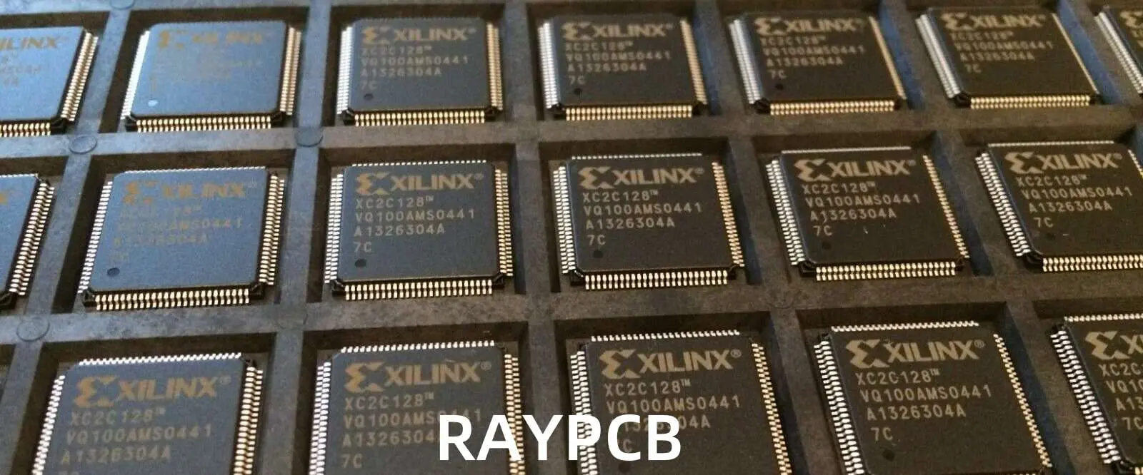
The XC2C128-6TQG144C is a powerful Complex Programmable Logic Device (CPLD) from Xilinx’s acclaimed CoolRunner-II family. This versatile semiconductor component represents a significant advancement in programmable logic technology, combining exceptional performance with remarkably low power consumption. As electronic designs continue to demand more flexibility, faster time-to-market, and energy efficiency, the XC2C128-6TQG144C stands as an ideal solution for a wide range of applications from portable devices to high-speed communication systems.

Understanding the XC2C128-6TQG144C

The XC2C128-6TQG144C is characterized by its part number, which provides key information about its specifications:

  • XC2C128: Identifies it as a 128-macrocell device in the CoolRunner-II family
  • 6: Speed grade (with a 5.7ns maximum pin-to-pin delay)
  • TQG144: Package type (144-pin Thin Quad Flat Package)
  • C: Commercial temperature grade (0ยฐC to 70ยฐC operating range)

This particular model balances power efficiency with high-speed operations, making it suitable for diverse applications in modern electronic design.

Key Features and Specifications

Core Specifications

The XC2C128-6TQG144C offers impressive technical specifications that position it as a versatile component in digital systems:

  • Logic Capacity: 128 macrocells organized in 8 function blocks
  • Gate Equivalent: Approximately 3,000 gates
  • I/O Capabilities: 100 user-configurable I/O pins
  • Performance: Maximum pin-to-pin delay of 5.7ns
  • Operating Voltage: 1.7V to 1.9V internal supply voltage
  • Package: 144-pin TQFP (20mm ร— 20mm)
  • Operating Temperature: Commercial grade (0ยฐC to 70ยฐC)
  • Programming: In-System Programmable (ISP) via IEEE 1532 (JTAG)

Advanced Architectural Features

The CoolRunner-II architecture incorporated in the XC2C128-6TQG144C provides several advanced features that enhance its versatility:

  1. Ultra-Low Power Consumption: The device implements innovative power-saving technologies that significantly reduce both standby and dynamic power consumption. This makes it ideal for battery-operated and portable applications.
  2. Advanced Interconnect Matrix (AIM): The function blocks are connected through a proprietary low-power interconnect structure that efficiently routes signals while minimizing power usage.
  3. Flexible I/O Banking: The XC2C128-6TQG144C features two I/O banks that support multiple voltage standards, allowing easy interfacing with 3.3V, 2.5V, 1.8V, and 1.5V devices.
  4. JEDEC I/O Standard Compatibility: Compatible with various industry-standard I/O interfaces, including LVCMOS, SSTL, and HSTL, enhancing integration capabilities.
  5. Schmitt-Trigger Inputs: Optional Schmitt-trigger inputs provide improved noise immunity, particularly useful for 1.5V I/O compatibility.
  6. DataGATE Technology: This feature allows designers to reduce power consumption by blocking input signals that are not contributing to active functions.
  7. Zero-Power Mode: When inactive, the device can enter an ultra-low power state, extending battery life in portable applications.

Performance Advantages

The XC2C128-6TQG144C delivers several significant performance advantages that make it an excellent choice for designers:

Speed and Responsiveness

With pin-to-pin delays as low as 5.7ns, the XC2C128-6TQG144C can handle high-speed operations efficiently. This responsiveness is crucial for applications requiring rapid data processing or real-time control.

Power Efficiency

The CoolRunner-II architecture is renowned for its exceptional power efficiency. By combining CMOS technology with advanced power management features, the XC2C128-6TQG144C achieves remarkably low power consumption without sacrificing performance.

Instant-On Capability

Unlike many FPGAs that require configuration time upon power-up, the XC2C128-6TQG144C is instantly operational when powered, making it ideal for applications that need immediate functionality.

Design Flexibility

The 128 macrocells provide ample resources for implementing complex logic functions, while the 100 user I/O pins offer extensive connectivity options for interfacing with other system components.

Applications

The XC2C128-6TQG144C finds applications across numerous industries due to its versatility, performance, and power efficiency:

Consumer Electronics

  • Portable Devices: Smartphones, tablets, and wearable technology benefit from the device’s low power consumption.
  • Home Entertainment Systems: The high-speed capabilities support audio/video processing and interface control.
  • Smart Home Devices: The flexibility and instant-on capabilities are ideal for IoT applications.

Industrial Systems

  • Control Systems: The deterministic performance and reliability make it suitable for industrial control applications.
  • Sensor Interfaces: The I/O capabilities facilitate connections to various sensors and actuators.
  • Human-Machine Interfaces: The speed and responsiveness support interactive control panels and displays.

Communications Equipment

  • Network Hardware: Routers, switches, and other networking equipment utilize the high-speed capabilities.
  • Protocol Bridges: The device can implement protocol conversion between different communication standards.
  • Line Cards: The compact form factor and performance suit telecommunications line card applications.

Computing Systems

  • PC Peripherals: Keyboard controllers, USB hubs, and other peripherals benefit from the fast response times.
  • Memory Controllers: The device can implement custom memory interfaces and controllers.
  • Bus Interfaces: Various computer bus protocols can be supported through customized implementations.

Design and Implementation

Development Tools

The XC2C128-6TQG144C is supported by Xilinx’s comprehensive design tool ecosystem:

  • ISE WebPACK: The free version of Xilinx’s Integrated Software Environment provides essential design tools for the CoolRunner-II family.
  • ISE Design Suite: The full-featured design environment offers advanced capabilities for complex designs.
  • Vivado Design Suite: Later versions of Xilinx’s design tools also support CoolRunner-II devices with enhanced features.

These tools provide a complete development environment, including schematic entry, HDL design, simulation, synthesis, implementation, and programming.

Design Methodologies

Designers can implement circuits on the XC2C128-6TQG144C using several methodologies:

  1. Schematic Capture: Creating designs using graphical schematic tools.
  2. Hardware Description Languages: Using VHDL or Verilog to describe circuit behavior.
  3. Behavioral Modeling: Implementing algorithms at a higher level of abstraction.
  4. Mixed-Mode Design: Combining schematic and HDL approaches for optimal results.

Programming and Configuration

The XC2C128-6TQG144C supports in-system programming through the IEEE 1532 (JTAG) interface, allowing for:

  • Initial Programming: Loading the initial configuration during production.
  • Field Updates: Updating the device’s functionality after deployment.
  • Debugging: Testing and troubleshooting through boundary scan operations.

Advantages Over Alternative Solutions

Compared to ASICs

  • Faster Time-to-Market: No fabrication delays or mask costs.
  • Field Reprogrammability: Updates and modifications can be implemented without hardware changes.
  • Lower Development Costs: No NRE (Non-Recurring Engineering) costs for production.

Compared to FPGAs

  • Lower Power Consumption: Typically uses less power than equivalent FPGA solutions.
  • Instant-On Capability: No configuration time required at power-up.
  • Deterministic Performance: More predictable timing characteristics.
  • Simpler Design Flow: Often requires fewer design iterations.

Compared to Microcontrollers

  • Higher Performance for Logic Functions: Parallel processing capabilities outperform sequential execution.
  • Lower Latency: Direct hardware implementation reduces response times.
  • Custom Functionality: Precisely tailored to application requirements without unused overhead.

Design Considerations

Power Management

To optimize power consumption when using the XC2C128-6TQG144C:

  1. Utilize DataGATE: Implement the DataGATE feature to block unwanted input transitions.
  2. I/O Bank Configuration: Configure I/O banks for the lowest acceptable voltage levels.
  3. Minimize Switching Activity: Design to reduce unnecessary signal transitions.
  4. Clock Management: Implement efficient clocking strategies to reduce dynamic power.

Thermal Management

The commercial temperature grade (0ยฐC to 70ยฐC) should be considered when designing systems:

  1. Adequate Airflow: Ensure sufficient cooling in enclosed systems.
  2. Thermal Design: Consider the device’s thermal characteristics in PCB layout.
  3. Environmental Factors: Account for ambient temperature in the deployment environment.

Signal Integrity

High-speed digital designs require careful attention to signal integrity:

  1. Controlled Impedance: Use properly designed PCB traces for high-speed signals.
  2. Decoupling Capacitors: Implement appropriate power supply decoupling.
  3. Ground Planes: Use solid ground planes to minimize noise and provide return paths.
  4. Termination: Consider termination for signals that require it.

Conclusion

The XC2C128-6TQG144C represents a compelling solution for digital design challenges across multiple industries. Its combination of high performance, low power consumption, and design flexibility makes it an excellent choice for applications ranging from portable consumer devices to industrial control systems.

As electronic designs continue to evolve, the balance of performance, power efficiency, and flexibility offered by the XC2C128-6TQG144C ensures its relevance in modern digital systems. Whether implementing simple glue logic or complex state machines, this versatile CPLD provides the resources, speed, and efficiency required by today’s demanding applications.

For designers seeking a reliable, efficient, and versatile programmable logic solution, the XC2C128-6TQG144C continues to be a valuable component in the digital designer’s toolkit.

ESP32 Arduino IDE Setup: Flashing Code for WROOM32 and C3

Are you looking to get started with ESP32 development using the Arduino IDE? Whether you’re working with the popular ESP32 WROOM32 or the newer ESP32-C3 boards, this comprehensive guide will walk you through the entire setup process. From installing the necessary software to troubleshooting common issues, you’ll learn everything needed to successfully flash code to your ESP32 devices.

YouTube video

Why Choose ESP32 for Your Projects?

The ESP32 microcontroller family has revolutionized IoT development with its powerful features and affordable price point. Before diving into the setup process, let’s understand what makes ESP32 boards so popular among hobbyists and professionals alike.

Features and Capabilities of ESP32 Boards

ESP32 boards pack impressive capabilities into a small form factor. They support both Wi-Fi and Bluetooth connectivity, feature dual-core processors (in the WROOM32 variant), and offer numerous GPIO pins for connecting external components. The ESP32-C3 variant brings RISC-V architecture to the table, offering excellent performance while maintaining compatibility with existing ESP32 code.

These versatile microcontrollers can operate on low power, making them ideal for battery-operated devices and IoT applications. With built-in touch sensors, temperature sensors, and hall effect sensors, ESP32 boards provide a complete solution for a wide range of projects.

Comparing WROOM32 and C3 Variants

When selecting an ESP32 board for your project, understanding the differences between variants is crucial:

  • ESP32 WROOM32: Features a dual-core processor, more GPIO pins, and generally higher processing power. Ideal for complex projects requiring substantial computational resources.
  • ESP32-C3: Utilizes a single-core RISC-V processor, offers smaller form factor, lower power consumption, and reduced cost. Perfect for simpler IoT applications where size and power efficiency are priorities.

Both variants support Arduino IDE programming, making them accessible to developers familiar with the Arduino ecosystem.

Setting Up Arduino IDE for ESP32 Development

Let’s start with the essential steps to configure your Arduino IDE for ESP32 programming.

Installing Arduino IDE

Before programming ESP32 boards, you’ll need the Arduino IDE installed on your computer. If you’re just starting with ESP32, Arduino IDE is recommended for its simplicity and intuitive interface.

The process to install Arduino IDE is straightforward:

  1. Visit the Arduino official website to download the latest version
  2. Select the appropriate installer for your operating system (Windows, macOS, or Linux)
  3. Follow the installation prompts to complete the setup

You can choose between Arduino IDE 1.x and the newer Arduino IDE 2.x versions. Both support ESP32 development, but the setup process differs slightly between them.

Adding ESP32 Board Support to Arduino IDE 1.x

To program the ESP32 using Arduino IDE, you’ll need to install an add-on that enables the ESP32 board compatibility with Arduino’s programming language. Follow these steps to add ESP32 support:

  1. Open Arduino IDE
  2. Navigate to File > Preferences
  3. In the “Additional Board Manager URLs” field, add: https://raw.githubusercontent.com/espressif/arduino-esp32/gh-pages/package_esp32_index.json
  4. Click “OK” to save the preferences
  5. Go to Tools > Board > Boards Manager
  6. Search for “ESP32”
  7. Find “ESP32 by Espressif Systems” and click “Install”
  8. Wait for the installation to complete and restart Arduino IDE

Adding ESP32 Board Support to Arduino IDE 2.x

For the newer Arduino IDE 2.x, the process to add ESP32 support is slightly different but equally straightforward. Here’s how:

  1. Open Arduino IDE 2.x
  2. Click the Boards Manager icon in the left sidebar (or go to Tools > Board > Boards Manager)
  3. Search for “ESP32”
  4. Find “ESP32 by Espressif Systems” and click “Install”
  5. Select version 2.0.11 or newer from the dropdown menu
  6. Wait for the installation to complete

Configuring Your ESP32 Board

After installing the ESP32 board support, you need to configure Arduino IDE for your specific board model.

Setting Up WROOM32 Boards

To configure Arduino IDE for ESP32 WROOM32 boards:

  1. Connect your ESP32 WROOM32 board to your computer via USB
  2. In Arduino IDE, go to Tools > Board > ESP32 Arduino
  3. Select “ESP32 Dev Module” or “DOIT ESP32 DEVKIT V1” (depending on your board model)
  4. Set the following parameters under the Tools menu:
    • Upload Speed: 921600
    • CPU Frequency: 240MHz
    • Flash Frequency: 80MHz
    • Flash Mode: QIO
    • Flash Size: 4MB
    • Partition Scheme: Default 4MB with spiffs
    • Core Debug Level: None
    • PSRAM: Disabled
  5. Under Tools > Port, select the COM port where your ESP32 is connected

If you don’t see any available ports, you may need to install the appropriate USB drivers for your board.

Setting Up ESP32-C3 Boards

For ESP32-C3 boards, the configuration is slightly different. After connecting your board to the computer, select the corresponding board model and port. Follow these steps:

  1. Connect your ESP32-C3 board to your computer via USB
  2. In Arduino IDE, go to Tools > Board > ESP32 Arduino
  3. Select “ESP32C3 Dev Module” or your specific C3 board model
  4. Configure the following settings:
    • Upload Speed: 460800
    • USB CDC On Boot: Enabled (important for ESP32-C3)
    • CPU Frequency: 160MHz
    • Flash Frequency: 80MHz
    • Flash Mode: QIO
    • Flash Size: 4MB
    • Partition Scheme: Default 4MB with spiffs
    • Core Debug Level: None
  5. Select the appropriate port under Tools > Port

Installing USB Drivers

Many ESP32 boards require specific USB drivers to be recognized by your computer.

Common Driver Types

ESP32 development boards typically use USB-to-serial converter chips that may require driver installation before you can upload code to your board. The most common types are:

  1. CP210x: Used in many ESP32 DevKit boards and the WROOM32 module
  2. CH340/CH341: Found in lower-cost ESP32 boards and many ESP32-C3 variants

Installing Drivers on Different Operating Systems

Driver installation varies by operating system:

Windows:

  1. Download the appropriate driver from the manufacturer’s website
  2. Run the installer and follow the prompts
  3. You may need to restart your computer after installation

macOS:

  1. Download the macOS version of the driver
  2. Open the installer package and follow the instructions
  3. You may need to authorize the driver in System Preferences > Security & Privacy

Linux:

  1. Most Linux distributions include the necessary drivers by default
  2. For some boards, you may need to add your user to the “dialout” group with the command: sudo usermod -a -G dialout $USER
  3. Log out and log back in for the changes to take effect

Uploading Your First Sketch

Now let’s test your setup by uploading a simple sketch to your ESP32.

Basic Blink Sketch

To test the ESP32 board installation, upload a simple code that blinks the on-board LED (typically connected to GPIO 2). Here’s a basic sketch to try:

cpp// Simple blink sketch for ESP32
// LED pin varies by board - GPIO 2 is common for WROOM32, GPIO 8 for many C3 boards

#define LED_PIN 2  // Change to 8 for ESP32-C3 if needed

void setup() {
  pinMode(LED_PIN, OUTPUT);
  Serial.begin(115200);
  Serial.println("ESP32 Blink Test");
}

void loop() {
  digitalWrite(LED_PIN, HIGH);
  Serial.println("LED ON");
  delay(1000);
  digitalWrite(LED_PIN, LOW);
  Serial.println("LED OFF");
  delay(1000);
}

Putting ESP32 in Boot Mode

Some ESP32 boards don’t automatically enter programming mode when uploading code. If you encounter issues, you may need to manually enter boot mode by pressing specific button combinations.

For WROOM32 boards:

  1. Press and hold the BOOT button
  2. Click the upload button in Arduino IDE
  3. When you see “Connecting…” in the console, release the BOOT button

For ESP32-C3 boards:

  1. Press and hold the BOOT button
  2. Press the RESET button once while holding BOOT
  3. Release the BOOT button
  4. Click upload in Arduino IDE

Monitoring Serial Output

After uploading your sketch:

  1. Open the Serial Monitor by clicking the icon in the top-right corner or navigating to Tools > Serial Monitor
  2. Set the baud rate to 115200
  3. You should see the “LED ON” and “LED OFF” messages alternating every second
  4. The onboard LED should blink accordingly

Troubleshooting Common Issues

Even with careful setup, you might encounter some challenges. Here are solutions to the most common problems.

Connection and Upload Problems

If you’re having trouble uploading code to your ESP32:

  1. Port not found:
    • Ensure your board is properly connected
    • Install or reinstall the appropriate USB drivers
    • Try a different USB cable (some cables are charge-only)
    • Try a different USB port on your computer
  2. Upload timeout: If you see the error “A fatal error occurred: Failed to connect to ESP32: Timed out… Connecting…” it means your ESP32 is not in flashing/uploading mode.
    • Follow the boot mode instructions mentioned earlier
    • For persistent issues, try lowering the upload speed in Tools menu
  3. Board not responding:
    • Press the reset button on your ESP32 board
    • Disconnect and reconnect the USB cable
    • Restart Arduino IDE

Serial Communication Issues

If you can upload code but don’t see serial output:

  1. No data in Serial Monitor: Lowering the baud rate can help stabilize the serial communication, especially if you’re using a lower-quality USB cable or a system with limited resources.
    • Ensure your Serial Monitor baud rate matches the one in your code (typically 115200)
    • Check that your code includes Serial.begin(115200) in the setup function
  2. Garbled characters:
    • Verify that the baud rate in Serial Monitor matches your code
    • Try a different USB cable or port
    • For ESP32-C3 boards, ensure “USB CDC On Boot” is enabled in the Tools menu

Advanced ESP32 Features with Arduino IDE

Once you’ve mastered the basics, you can explore more advanced capabilities of your ESP32 board.

Wi-Fi and Bluetooth Functionality

ESP32’s built-in wireless connectivity can be easily accessed through Arduino libraries:

  1. For Wi-Fi, use the WiFi.h library to connect to networks, create access points, or implement web servers
  2. For Bluetooth, the BluetoothSerial.h library enables classic Bluetooth functionality, while BLEDevice.h provides Bluetooth Low Energy support

Working with ESP32 Peripherals

ESP32 boards offer numerous peripherals that can be controlled through Arduino code:

  1. Analog-to-Digital Conversion: Use analogRead() to read values from the ADC pins
  2. Digital-to-Analog Conversion: The dacWrite() function outputs analog voltages on supported pins
  3. Touch Sensors: Access the capacitive touch sensors with touchRead() functions
  4. PWM Control: Create precise PWM signals using the ledc functions for motor control or LED dimming

File System and Data Storage

ESP32 supports various file systems for data storage:

  1. SPIFFS: A simple file system for the flash memory, accessible through the SPIFFS library
  2. LittleFS: A more robust alternative to SPIFFS with better wear leveling
  3. SD Card: Interface with SD cards using the SD library for expanded storage capacity

Project Examples for ESP32 WROOM32 and C3

Let’s explore some practical applications for your newly configured ESP32 boards.

IoT Weather Station

Create a simple weather station that monitors temperature, humidity, and pressure:

  1. Connect BME280 or DHT22 sensors to your ESP32
  2. Read sensor data at regular intervals
  3. Send data to a cloud platform like ThingSpeak or create a local web server to display readings
  4. Implement sleep modes to conserve battery life for remote installations

Smart Home Controller

Transform your ESP32 into a smart home hub:

  1. Use relays to control household appliances
  2. Implement a web interface or mobile app for remote control
  3. Add sensors to create automation rules based on environmental conditions
  4. Integrate with existing smart home platforms like Home Assistant or MQTT brokers

Differences in Implementation Between WROOM32 and C3

When developing projects for different ESP32 variants, keep these considerations in mind:

  1. GPIO Assignments: Pin numbering and available pins differ between models
  2. Power Consumption: C3 generally consumes less power, making it better for battery-operated devices
  3. Processing Power: WROOM32’s dual-core architecture handles complex tasks more efficiently
  4. Memory Constraints: Adjust your code complexity based on the available RAM and flash memory

Conclusion

Setting up the Arduino IDE for ESP32 development opens up a world of possibilities for your DIY electronics projects. Whether you’re working with the powerful ESP32 WROOM32 or the energy-efficient ESP32-C3, this guide has equipped you with the knowledge to install the necessary software, configure your boards, and start programming.

Remember that the ESP32 ecosystem is constantly evolving, with new board variants and software updates appearing regularly. Stay connected with the ESP32 community through forums and the official Espressif documentation to keep up with the latest developments.

With your ESP32 Arduino setup complete, you’re ready to explore the full potential of these versatile microcontrollers. From simple LED blink projects to sophisticated IoT applications, the ESP32 platform offers the perfect balance of performance, features, and affordability for makers at all skill levels.

Altera Programmer Guide: JTAG Programming for CPLD & FPGA (MAX II, Cyclone IV, EPM240T100C5N) โ€“ Quartus & MAX+II Support & Downloads

1. Introduction to Altera Programmer

In the world of programmable logic devices, the Altera Programmer stands as a crucial tool for engineers and developers working with Complex Programmable Logic Devices (CPLDs) and Field-Programmable Gate Arrays (FPGAs). This comprehensive guide will walk you through the intricacies of using an Altera Programmer, with a focus on JTAG programming for popular devices such as MAX II, Cyclone IV, and the EPM240T100C5N.

What is an Altera Programmer?

An Altera Programmer is a hardware device used to configure Altera (now part of Intel) CPLDs and FPGAs. It serves as the bridge between your development computer and the target device, allowing you to download your designed logic onto the chip.

Key Uses for CPLD and FPGA Devices

CPLDs and FPGAs are versatile semiconductor devices that can be programmed to perform a wide range of digital logic functions. Some key applications include:

  1. Prototyping complex digital systems
  2. Implementing custom interfaces and protocols
  3. Accelerating specific computational tasks
  4. Serving as glue logic in larger electronic systems
YouTube video

Overview of Supported Devices

This guide will focus on programming three popular Altera devices:

  1. MAX II: A family of low-cost, non-volatile CPLDs
  2. Cyclone IV: A series of low-power, high-functionality FPGAs
  3. EPM240T100C5N: A specific MAX II CPLD with 240 macrocells

2. Understanding JTAG Programming

JTAG (Joint Test Action Group) programming is the primary method used for configuring Altera devices. Let’s delve into what JTAG is and why it’s crucial for Altera device programming.

What is JTAG?

JTAG, officially known as IEEE 1149.1 Standard Test Access Port and Boundary-Scan Architecture, is a widely adopted industry standard for testing and programming integrated circuits. It provides a standardized interface for accessing and controlling the pins of a device without direct physical contact.

Why JTAG is Used in Altera Device Programming

JTAG is the preferred method for programming Altera devices due to several advantages:

  1. Standardization: JTAG is an industry-standard protocol, ensuring compatibility across different tools and devices.
  2. In-System Programming: Devices can be programmed while soldered onto a PCB, eliminating the need for specialized sockets.
  3. Daisy-Chaining: Multiple devices can be programmed through a single JTAG interface.
  4. Debugging Capabilities: JTAG allows for real-time debugging and monitoring of device operations.

Comparison of JTAG vs. Other Programming Methods

While JTAG is the primary programming method for Altera devices, it’s worth comparing it to alternative approaches:

  1. JTAG vs. In-Socket Programming:
    • JTAG: In-system programming, no special socket required
    • In-Socket: Requires removing the chip and using a dedicated programmer
  2. JTAG vs. Serial Programming:
    • JTAG: Faster programming speeds, more debugging features
    • Serial: Simpler interface, but limited functionality
  3. JTAG vs. Passive Serial:
    • JTAG: More versatile, supports both programming and debugging
    • Passive Serial: Simpler, but limited to programming only

3. Required Tools & Software

To successfully program Altera devices, you’ll need specific software tools. Let’s explore the essential software required for Altera programming.

Overview of Quartus Prime and MAX+II Programmer

  1. Quartus Prime:
    • Comprehensive development environment for Altera FPGAs and CPLDs
    • Supports device programming, synthesis, place-and-route, and timing analysis
    • Available in different editions: Lite (free), Standard, and Pro
  2. MAX+II Programmer:
    • Legacy tool specifically designed for older MAX series CPLDs
    • Simpler interface focused solely on device programming
    • Still relevant for programming certain MAX II devices

Where to Download Quartus and MAX+II Software

You can download the necessary software from the official Intel FPGA website:

  1. Quartus Prime: https://www.intel.com/content/www/us/en/software/programmable/quartus-prime/overview.html
  2. MAX+II Programmer: https://www.intel.com/content/www/us/en/programmable/downloads/software/max2/max2-index.html

System Requirements and Installation Tips

Before installing Quartus Prime or MAX+II Programmer, ensure your system meets the following requirements:

  1. Operating System:
    • Windows 10/8.1/7 (64-bit versions)
    • Red Hat Enterprise Linux 6 or 7
    • SUSE Enterprise Linux 11 or 12
  2. Processor: Multi-core 64-bit processor (Intel Core i5 or equivalent recommended)
  3. RAM: 8 GB minimum, 16 GB or more recommended
  4. Disk Space: 50 GB minimum for a full installation

Installation Tips:

  1. Download the latest version of Quartus Prime or MAX+II Programmer
  2. Run the installer with administrative privileges
  3. Choose a custom installation path if desired (avoid spaces in the path)
  4. Install device support for your specific Altera devices (MAX II, Cyclone IV)
  5. Restart your computer after installation to ensure all components are properly configured

4. Hardware Setup

Proper hardware setup is crucial for successful Altera device programming. Let’s explore the supported programmers and how to connect them to your target devices.

Supported Altera Programmers

Altera offers several programming hardware options, with the most common being:

  1. USB-Blaster:
    • Original USB-based programmer for Altera devices
    • Widely supported across different software versions
  2. USB-Blaster II:
    • Newer version with improved performance
    • Supports faster programming speeds and additional features

Both programmers are compatible with a wide range of Altera devices, including MAX II, Cyclone IV, and the EPM240T100C5N.

Connecting Your Programmer to MAX II / Cyclone IV Devices

To connect your Altera Programmer to your target device:

  1. Identify the JTAG header on your development board or custom PCB
  2. Connect the 10-pin header of the USB-Blaster or USB-Blaster II to the JTAG pins
  3. Ensure proper orientation (Pin 1 is typically marked on both the cable and board)
  4. Connect the USB end of the programmer to your computer
  5. Power on your target board

Pinout Diagrams and Board Preparation

For successful programming, you need to understand the JTAG pinout:

  1. TCK: Test Clock
  2. TDO: Test Data Out
  3. TDI: Test Data In
  4. TMS: Test Mode Select
  5. nTRST: Test Reset (optional)

Typical 10-pin JTAG header pinout:

 9 7 5 3 1
10 8 6 4 2

1: TCK 2: GND 3: TDO 4: VCC (3.3V) 5: TMS 6: N/C 7: N/C 8: N/C 9: TDI 10: GND

Ensure your board is properly prepared:

  1. Verify power supply connections
  2. Check for any required jumper settings
  3. Confirm that the JTAG pins are not shared with other functions

Read more about:

5. Programming CPLDs and FPGAs

Now that we’ve covered the basics, let’s dive into the step-by-step process of programming Altera devices using JTAG.

Step-by-Step Guide: Programming EPM240T100C5N (MAX II)

  1. Launch Quartus Prime or MAX+II Programmer
  2. Click “Hardware Setup” and select your USB-Blaster
  3. Choose “JTAG” as the programming mode
  4. Click “Add File” and select your .pof file for the EPM240T100C5N
  5. Ensure the “Program/Configure” option is checked
  6. Click “Start” to begin programming
  7. Wait for the operation to complete (indicated by a blue progress bar)
  8. Verify successful programming in the programmer window

Programming Cyclone IV Using Quartus Prime

  1. Open Quartus Prime and your Cyclone IV project
  2. Compile your design to generate a .sof file
  3. Open the Programmer tool (Tools > Programmer)
  4. Select your USB-Blaster in the Hardware Setup
  5. Click “Auto Detect” to identify the JTAG chain
  6. Right-click the detected Cyclone IV device and choose “Change File”
  7. Select your compiled .sof file
  8. Check the “Program/Configure” box
  9. Click “Start” to program the device
  10. Monitor the progress and confirm successful programming

Using .pof and .sof Files with Altera Programmer Tools

Understanding file types is crucial for effective Altera programming:

  1. .sof (SRAM Object File):
    • Used for volatile programming of FPGAs
    • Configuration is lost when power is removed
    • Typically used during development and debugging
  2. .pof (Programmer Object File):
    • Used for non-volatile programming of CPLDs and some FPGAs
    • Configuration is retained after power cycling
    • Used for production programming or when persistent configuration is needed

To convert between file types:

  1. Open Quartus Prime
  2. Go to File > Convert Programming Files
  3. Select the output file type (.pof or .sof)
  4. Add your input file and configure any necessary options
  5. Click “Generate” to create the new file

6. Troubleshooting Common Issues

Even with careful setup, you may encounter issues when programming Altera devices. Here are some common problems and their solutions.

Programmer Not Detected

If your Altera Programmer isn’t recognized:

  1. Check USB connections and try a different port
  2. Reinstall USB-Blaster drivers (found in Quartus installation directory)
  3. Verify the programmer is listed in Device Manager
  4. Try a different USB cable

JTAG Chain Errors

When encountering JTAG chain issues:

  1. Ensure all devices in the chain are powered on
  2. Check JTAG connections for loose or incorrect wiring
  3. Verify the JTAG chain in Quartus (Auto Detect feature)
  4. Try reducing the JTAG clock frequency in the programmer settings

Power Supply and Cable Issues

Power-related problems can cause programming failures:

  1. Verify your board is receiving the correct voltage
  2. Check for any required external power supplies
  3. Ensure the JTAG header is properly connected
  4. Look for any signs of physical damage to cables or connectors

Fixing Quartus-Related Software Problems

Software issues can also hinder programming:

  1. Update Quartus Prime to the latest version
  2. Reinstall device support packages
  3. Clear the Quartus Prime cache (Tools > Options > General > Clear Compilation Database)
  4. Verify project settings match your target device

7. Best Practices for Reliable Programming

To ensure consistent and reliable programming of Altera devices, follow these best practices:

Tips for Consistent JTAG Programming

  1. Use high-quality, short JTAG cables to minimize signal integrity issues
  2. Implement proper power sequencing for your target board
  3. Avoid hot-plugging JTAG connections; always power down before connecting/disconnecting
  4. Use the appropriate programming file type (.sof for volatile, .pof for non-volatile)
  5. Verify device ID and JTAG chain integrity before each programming session

Firmware and Driver Updates

Keeping your software and firmware up-to-date is crucial:

  1. Regularly check for Quartus Prime updates
  2. Update USB-Blaster firmware through Quartus (Tools > Programmer > Hardware Setup)
  3. Ensure your computer’s USB drivers are current
  4. Subscribe to Intel FPGA notifications for critical updates

Verifying Programmed Logic

After programming, always verify your design:

  1. Use the “Verify” option in the programmer tool
  2. Implement a simple test design (e.g., LED blinker) to confirm basic functionality
  3. Utilize Quartus SignalTap II Logic Analyzer for in-depth verification
  4. Perform thorough functional testing of your programmed design

8. Support & Downloads

For additional resources and support, refer to these official Intel/Altera links:

Official Intel/Altera Support Links

  1. Intel FPGA Support Center: https://www.intel.com/content/www/us/en/programmable/support/support-resources.html
  2. Altera Programming Hardware Support: https://www.intel.com/content/www/us/en/programmable/support/support-resources/programming-hardware.html

Download Links for Legacy Tools

  1. MAX+PLUS II Software: https://www.intel.com/content/www/us/en/programmable/downloads/software/max2/max2-index.html
  2. Quartus II Web Edition (13.0sp1): https://www.intel.com/content/www/us/en/programmable/downloads/software/quartus-ii-we/130sp1.html

Documentation and User Manual Links

  1. MAX II Device Handbook: https://www.intel.com/content/www/us/en/programmable/products/cpld/max-series/max-ii/support.html
  2. Cyclone IV Device Handbook: https://www.intel.com/content/www/us/en/programmable/products/fpga/cyclone-series/cyclone-iv/support.html
  3. Quartus Prime Pro Edition User Guide: Programming and Configuration: https://www.intel.com/content/www/us/en/programmable/documentation/ftt1513991830769.html

9. Frequently Asked Questions (FAQs)

How do I install an Altera Programmer driver?

To install the Altera Programmer driver:

  1. Connect the USB-Blaster to your computer
  2. Open Device Manager
  3. Locate the “Altera USB-Blaster” under “Other devices”
  4. Right-click and select “Update Driver Software”
  5. Choose “Browse my computer for driver software”
  6. Navigate to your Quartus installation directory (e.g., C:\altera\quartus\drivers)
  7. Select the appropriate driver folder and click “Next”
  8. Follow the prompts to complete the installation

Which programmer should I use for MAX II devices?

For MAX II devices like the EPM240T100C5N, both the USB-Blaster and USB-Blaster II are suitable. The original USB-Blaster is widely supported across different software versions, while the USB-Blaster II offers improved performance. Choose based on your specific needs and software compatibility.

Can I use Quartus Lite for programming CPLDs?

Yes, Quartus Prime Lite Edition can be used for programming most Altera CPLDs, including MAX II devices like the EPM240T100C5N. However, keep in mind that Quartus Prime Lite may have some limitations compared to the Standard or Pro editions:

  1. Limited device support (but covers most common CPLDs and low-end FPGAs)
  2. Fewer advanced optimization features
  3. Restricted use of some high-end IP cores

For most CPLD programming tasks, Quartus Prime Lite should be sufficient.

10. Conclusion

Mastering the use of an Altera Programmer for JTAG programming of CPLDs and FPGAs is an essential skill for digital design engineers. Throughout this guide, we’ve explored the intricacies of programming devices such as the MAX II, Cyclone IV, and specifically the EPM240T100C5N.

Summary of Programming Workflow

The general workflow for programming Altera devices can be summarized as follows:

  1. Install the necessary software (Quartus Prime or MAX+II Programmer)
  2. Set up your hardware, connecting the Altera Programmer to your target device
  3. Create or open your design project in Quartus Prime
  4. Compile your design to generate programming files (.sof or .pof)
  5. Use the Programmer tool to download the configuration to your device
  6. Verify successful programming and test your design’s functionality

Recommended Programmer Tools

For most Altera device programming tasks, we recommend:

  1. Hardware: USB-Blaster or USB-Blaster II
  2. Software: Quartus Prime (latest version compatible with your device)

These tools provide a robust and flexible platform for programming a wide range of Altera CPLDs and FPGAs.

Encouragement to Explore More Altera Resources

As you continue your journey with Altera programmable logic devices, we encourage you to:

  1. Explore the extensive documentation available on the Intel FPGA website
  2. Participate in online forums and communities dedicated to FPGA development
  3. Experiment with different devices and more complex designs
  4. Stay updated with the latest tools and technologies in the field of programmable logic

By mastering the Altera Programmer and associated tools, you’ve taken a significant step in the world of digital design. The skills you’ve acquired will serve as a strong foundation for tackling more advanced projects and pushing the boundaries of what’s possible with programmable logic.

Remember, the field of FPGAs and CPLDs is constantly evolving, so continue learning and exploring new techniques to stay at the forefront of this exciting technology. Happy programming!

CoolRunner-II CPLD Guide: Features, Applications, and Development Board Setup

Introduction

In the ever-evolving world of digital electronics, programmable logic devices (PLDs) have revolutionized the way engineers design and implement complex digital systems. Among these versatile devices, the CoolRunner-II CPLD family by Xilinx stands out as a popular choice for many applications. This guide will explore the features, applications, and setup process of the CoolRunner-II CPLD, with a focus on the widely used XC2C64A model.

The CoolRunner-II CPLD, also known as CoolRunner II or CoolRunner 2, continues to be a go-to solution for designers seeking low-power, high-performance programmable logic. Its enduring popularity stems from its unique combination of ultra-low power consumption, instant-on capability, and versatile features that make it ideal for a wide range of applications.

In this comprehensive guide, we’ll delve into the key features of the CoolRunner-II CPLD, explore its typical applications, and provide a step-by-step tutorial for setting up and using the CoolRunner-II CPLD starter board and development board. Whether you’re a seasoned engineer or a newcomer to the world of programmable logic, this guide will equip you with the knowledge to harness the power of the CoolRunner-II CPLD in your projects.

YouTube video

1. What is the CoolRunner-II CPLD?

Definition of a CPLD

A Complex Programmable Logic Device (CPLD) is a type of programmable logic device that allows designers to implement custom digital circuits. CPLDs consist of a set of logic blocks connected by a programmable interconnect matrix, enabling the creation of complex digital systems on a single chip.

Brief History of the Xilinx CoolRunner-II CPLD Family

The CoolRunner-II CPLD family was introduced by Xilinx in the early 2000s as a successor to the original CoolRunner series. It was designed to meet the growing demand for low-power, high-performance programmable logic in portable and battery-operated devices.

Differences Between CoolRunner II and Earlier Generations

CoolRunner-II CPLDs offer several improvements over their predecessors:

  1. Lower power consumption
  2. Higher operating speeds
  3. Increased logic density
  4. Enhanced I/O capabilities
  5. Improved design software support

Key Models

The CoolRunner-II CPLD family includes several models, with the XC2C64A being one of the most popular. Other models in the series include:

  • XC2C32A
  • XC2C128
  • XC2C256
  • XC2C384
  • XC2C512

Each model offers different numbers of macrocells and I/O pins, allowing designers to choose the most appropriate device for their specific requirements.

Read more about:

2. Key Features of CoolRunner-II CPLDs

xilinx-spartan-6-fpga-tutorial

Ultra-Low Power Operation

One of the standout features of the CoolRunner-II CPLD is its ultra-low power consumption. It offers two power modes:

  1. Zero Power Mode: Draws minimal current when the device is inactive
  2. Turbo Mode: Provides high-speed operation when needed

This flexibility allows designers to optimize power consumption based on the application’s requirements.

High-Speed Logic Performance

CoolRunner-II CPLDs offer excellent performance with:

  • System frequencies up to 320 MHz
  • Pin-to-pin delays as low as 3.5 ns

Instant-On Capability

Unlike many FPGAs, CoolRunner-II CPLDs are instantly operational upon power-up, making them ideal for applications that require immediate functionality.

High Density and Scalability

The CoolRunner-II CPLD family offers a range of densities, from 64 to 512 macrocells, allowing designers to choose the right size for their application while maintaining a consistent architecture across the family.

Low Pin-to-Pin Delay

With pin-to-pin delays as low as 3.5 ns, CoolRunner-II CPLDs are well-suited for high-speed interfacing and glue logic applications.

I/O Standards Support

CoolRunner-II CPLDs support various I/O standards, including:

  • LVCMOS (1.5V, 1.8V, 2.5V, 3.3V)
  • LVTTL
  • HSTL
  • SSTL

This versatility allows for easy integration with a wide range of other components and systems.

Internal Clocking Flexibility

The devices offer multiple clock sources and dividers, enabling designers to create complex timing schemes within a single CPLD.

Software Support

Xilinx provides robust software support for CoolRunner-II CPLDs through:

  • ISE WebPACK (for older versions)
  • Vivado Design Suite (for newer projects)

These tools offer a comprehensive development environment for designing, synthesizing, and implementing CPLD projects.

3. Common Applications of CoolRunner-II CPLD

Glue Logic in Embedded Systems

CoolRunner-II CPLDs excel at providing glue logic in embedded systems, integrating various components and interfaces efficiently.

Low-Power Handheld and Portable Electronics

The ultra-low power consumption of CoolRunner-II CPLDs makes them ideal for battery-operated devices such as:

  • Smartphones
  • Tablets
  • Wearable technology

Consumer Electronics

CoolRunner-II CPLDs find applications in various consumer electronics, including:

  • MP3 players
  • GPS devices
  • Digital cameras

Industrial Automation and Control Systems

In industrial settings, CoolRunner-II CPLDs are used for:

Interface Bridging

CoolRunner-II CPLDs are excellent for bridging different communication protocols, such as:

  • UART to SPI
  • I2C to Parallel bus
  • Legacy interfaces to modern standards

4. CoolRunner-II vs. Other CPLDs and FPGAs

Comparison with Traditional FPGAs

While FPGAs offer higher logic density and more advanced features, CoolRunner-II CPLDs have several advantages:

  1. Lower power consumption
  2. Faster start-up time
  3. Simpler design process
  4. Lower cost for smaller designs

When to Choose a CPLD Over an FPGA

Choose a CoolRunner-II CPLD when:

  • Ultra-low power consumption is critical
  • Instant-on functionality is required
  • The design is relatively simple and doesn’t require extensive resources
  • Cost is a significant factor

Advantages and Limitations

Advantages:

  • Ultra-low power consumption
  • Instant-on capability
  • Simple design process
  • Non-volatile configuration storage

Limitations:

  • Lower logic density compared to FPGAs
  • Limited advanced features (e.g., no DSP blocks or embedded processors)

5. Introduction to the CoolRunner-II CPLD Starter Board

What is the CoolRunner-II CPLD Starter Board?

The CoolRunner-II CPLD starter board is an evaluation and development platform designed to help engineers and hobbyists get started with CoolRunner-II CPLDs. It typically features an XC2C64A CoolRunner-II CPLD and various peripherals for prototyping and testing designs.

Key Features and Specifications

  • XC2C64A CoolRunner-II CPLD
  • On-board voltage regulators
  • JTAG programming interface
  • User-configurable clock sources
  • Multiple I/O expansion headers

Included Peripherals

  • Push-button switches
  • LED indicators
  • 7-segment display
  • Clock oscillator
  • Expansion headers for custom add-ons

6. Setting Up the CoolRunner-II Development Board

Unboxing the CoolRunner-II Development Board

When you receive your CoolRunner-II development board, carefully unpack it and check for any visible damage. The package should include:

  • CoolRunner-II development board
  • USB cable
  • Quick start guide
  • Any additional documentation or accessories

Required Tools and Software

To begin development with the CoolRunner-II CPLD, you’ll need:

  1. Xilinx ISE WebPACK (for older versions) or Vivado Design Suite
  2. USB programmer cable (usually included with the board)
  3. A computer running Windows or Linux

Installing Drivers and Software

  1. Download and install the appropriate Xilinx design software (ISE WebPACK or Vivado)
  2. Install any necessary USB drivers for the programming cable
  3. Update your system’s environment variables if required

First Connection Setup

  1. Connect the USB cable between your computer and the CoolRunner-II development board
  2. Power on the board (if it has a separate power switch)
  3. Verify that the board is recognized by your computer

Configuring the XC2C64A CoolRunner-II CPLD

  1. Launch the Xilinx design software
  2. Create a new project, selecting the XC2C64A as the target device
  3. Write your VHDL or Verilog code
  4. Synthesize and implement the design
  5. Generate the programming file
  6. Use the programming tool to configure the CPLD on the development board

7. First Project: Hello World with CoolRunner-II

Simple Project: Blinking LED

Let’s create a simple “Hello World” project that blinks an LED on the CoolRunner-II development board.

Writing a Basic VHDL Program

Here’s a simple VHDL code to blink an LED:

vhdlๅคๅˆถlibrary IEEE;
use IEEE.STD_LOGIC_1164.ALL;
use IEEE.NUMERIC_STD.ALL;

entity blink_led is
    Port ( clk : in STD_LOGIC;
           led : out STD_LOGIC);
end blink_led;

architecture Behavioral of blink_led is
    signal counter : unsigned(23 downto 0) := (others => '0');
begin
    process(clk)
    begin
        if rising_edge(clk) then
            counter <= counter + 1;
            if counter(23) = '1' then
                led <= '1';
            else
                led <= '0';
            end if;
        end if;
    end process;
end Behavioral;

Synthesizing, Implementing, and Programming the Device

  1. Create a new project in Xilinx ISE or Vivado
  2. Add the VHDL file to your project
  3. Set the XC2C64A as the target device
  4. Run synthesis and implementation
  5. Generate the programming file
  6. Use the programmer tool to configure the CPLD

Troubleshooting Tips for Beginners

  • Double-check your pin assignments in the constraints file
  • Verify that the clock source is correctly configured
  • Use the software’s built-in simulation tools to test your design before programming
  • If the LED doesn’t blink, try adjusting the counter size or clock frequency

8. Expanding Your CoolRunner-II Projects

Using Onboard Switches and LEDs for Input/Output

Expand your projects by incorporating the onboard switches and LEDs:

  • Use switches as input signals
  • Control multiple LEDs for more complex output patterns
  • Implement debouncing for switch inputs

Creating State Machines

State machines are powerful tools for controlling system behavior:

  • Implement a simple traffic light controller
  • Create a sequence detector using switch inputs
  • Design a basic elevator controller

Interface Examples: UART, SPI, I2C Bridging

CoolRunner-II CPLDs excel at interfacing different protocols:

  • Implement a UART to SPI bridge
  • Create an I2C to parallel bus converter
  • Design a custom communication protocol using available I/O

Power Optimization Tricks for Mobile Designs

To maximize battery life in portable applications:

  • Utilize the CoolRunner-II’s power-down modes
  • Implement clock gating for unused modules
  • Use the lowest possible operating voltage for your design

9. Where to Buy CoolRunner-II CPLD Boards and Parts

Recommended Vendors and Distributors

  • Digikey
  • Mouser Electronics
  • Arrow Electronics
  • Avnet

Finding an XC2C64A CoolRunner-II CPLD Development Board Affordably

  • Check for educational discounts if you’re a student or academic institution
  • Look for bundle deals that include software and accessories
  • Consider purchasing refurbished or older model boards for cost savings

Tips for Checking Compatibility and Authenticity

  • Verify that the board supports the specific CoolRunner-II CPLD model you need
  • Check for official Xilinx branding and documentation
  • Ensure the board is compatible with your version of Xilinx design software

Conclusion

The Xilinx CoolRunner-II CPLD remains a popular choice for designers seeking a low-power, versatile programmable logic solution. Its unique combination of ultra-low power consumption, instant-on capability, and robust feature set makes it ideal for a wide range of applications, from portable electronics to industrial control systems.

By starting with simple projects and gradually exploring more advanced features, you can unlock the full potential of the CoolRunner-II CPLD. The CoolRunner II development board provides an excellent platform for learning and prototyping, allowing you to bring your digital designs to life quickly and efficiently.

As you continue your journey with CoolRunner-II CPLDs, remember to experiment, explore new applications, and leverage the wealth of resources available from Xilinx and the broader CPLD community. With its enduring relevance and capabilities, the CoolRunner-II CPLD is sure to remain a valuable tool in your digital design toolkit for years to come.

Frequently Asked Questions (FAQ)

Q1: Is CoolRunner-II still supported by Xilinx?

A: While newer Xilinx products have been introduced, CoolRunner-II CPLDs are still supported through the Xilinx ISE WebPACK software. However, they are not supported in the newer Vivado Design Suite.

Q2: What is the difference between CoolRunner-II and Spartan FPGA?

A: CoolRunner-II is a CPLD family optimized for low power and instant-on applications, while Spartan FPGAs offer higher logic density and more advanced features but typically consume more power and require configuration upon startup.

Q3: Can I use CoolRunner-II CPLDs in new designs?

A: Yes, CoolRunner-II CPLDs are still suitable for new designs, especially in applications requiring low power consumption and instant-on functionality. However, consider future availability and support when making long-term design decisions.

Q4: What programming languages can I use with CoolRunner-II CPLDs?

A: CoolRunner-II CPLDs can be programmed using hardware description languages (HDLs) such as VHDL and Verilog. The choice between these languages often depends on personal preference or project requirements.

Q5: How does the power consumption of CoolRunner-II compare to other CPLDs?

A: CoolRunner-II CPLDs are known for their ultra-low power consumption, often outperforming other CPLD families in this aspect. This makes them particularly suitable for battery-operated and portable devices.

XC7A100T-1CSG324C FPGA: Datasheet, Pinout, Features & Pricing

Xilinx Artix 7

Introduction

In the ever-evolving world of digital electronics, Field-Programmable Gate Arrays (FPGAs) have become indispensable components for designers and engineers. Among the myriad of FPGA options available, the XC7A100T-1CSG324C stands out as a powerful and versatile choice. This comprehensive guide delves into the details of this Xilinx Artix-7 FPGA, exploring its datasheet, pinout configuration, key features, and pricing information. Whether you’re a seasoned engineer or a curious enthusiast, this article will provide valuable insights into the capabilities and applications of the XC7A100T-1CSG324C.

Understanding the XC7A100T-1CSG324C

Overview of the Xilinx Artix-7 Family

The XC7A100T-1CSG324C is part of the Xilinx Artix-7 FPGA family, known for its balance of low power consumption and high performance. Artix-7 FPGAs are designed to meet the needs of cost-sensitive applications while delivering impressive processing capabilities.

Decoding the Part Number

Let’s break down the part number to understand its specifications:

  • XC7: Indicates it’s a 7-series Xilinx FPGA
  • A: Denotes the Artix-7 family
  • 100T: Represents the device size (100K logic cells)
  • 1: Speed grade (standard performance)
  • CSG324: Chip-Scale Ball Grid Array (CS-BGA) package with 324 pins
  • C: Commercial temperature grade (0ยฐC to 85ยฐC)

XC7A100T-1CSG324C Datasheet Highlights

The datasheet for the XC7A100T-1CSG324C provides crucial information for designers and engineers. Here are some key specifications:

Logic Resources

  • Logic Cells: 101,440
  • CLB Flip-Flops: 126,800
  • CLB LUTs: 63,400
  • Maximum Distributed RAM (Kb): 1,188

Memory Resources

  • Block RAM Blocks: 135
  • Block RAM (Kb): 4,860
  • Total Block RAM (Mb): 4.9

Clock Management

  • MMCMs: 6
  • PLLs: 6

DSP Resources

  • DSP Slices: 240

I/O Resources

  • Maximum Single-Ended I/O: 210
  • Maximum Differential I/O Pairs: 100

Transceiver Resources

  • GTP Transceivers: 4

Package Information

  • Body Size: 15 x 15 mm
  • Ball Pitch: 0.8 mm
  • Total Pins: 324

Read more about:

Pinout Configuration

Xilinx Artix-7 FPGA

Understanding the pinout of the XC7A100T-1CSG324C is crucial for proper PCB design and integration. The 324-pin CSG package offers a compact form factor with ample I/O capabilities.

Key Pinout Sections

  1. Power Supply Pins: Multiple VCC and GND pins for core, auxiliary, and I/O power.
  2. Configuration Pins: Dedicated pins for device configuration and programming.
  3. Clock Input Pins: Specialized pins for high-speed clock inputs.
  4. User I/O Pins: General-purpose input/output pins, configurable for various standards.
  5. Transceiver Pins: High-speed serial I/O pins for GTP transceivers.
  6. JTAG Interface Pins: For boundary scan and device programming.

Pinout Considerations

  • Bank Organization: I/O pins are organized into banks, each supporting different voltage standards.
  • Differential Pairs: Certain pins can be configured as differential pairs for high-speed signaling.
  • Special Function Pins: Some pins have dual functionality, serving as both user I/O and special functions like configuration or clocking.

Key Features of the XC7A100T-1CSG324C

The XC7A100T-1CSG324C boasts a range of features that make it suitable for various applications. Let’s explore some of its standout capabilities:

1. Low Power Consumption

One of the hallmarks of the Artix-7 family is its energy efficiency. The XC7A100T-1CSG324C incorporates several power-saving features:

  • Intelligent Clock Gating: Automatically reduces dynamic power consumption by disabling unused clock networks.
  • Flexible Power Management: Allows designers to optimize power usage based on performance requirements.
  • Low-Power Gigabit Transceivers: GTP transceivers offer high-speed communication with minimal power overhead.

2. High-Performance DSP Capabilities

With 240 DSP slices, the XC7A100T-1CSG324C excels in digital signal processing applications:

  • Advanced DSP48E1 Slices: Support a wide range of symmetric and asymmetric filter structures.
  • High-Speed Arithmetic: Capable of performing up to 930 GMACs (Giga Multiply-Accumulate Operations per Second).
  • Flexible Precision: Supports various data widths, from 8-bit to 48-bit operations.

3. Versatile Memory Options

The XC7A100T-1CSG324C offers a variety of memory resources to suit different application needs:

  • Block RAM: 4.9 Mb of fast, on-chip memory configurable as single or dual-port RAM.
  • Distributed RAM: Up to 1,188 Kb of RAM implemented using LUTs for small, distributed memory structures.
  • Shift Register LUTs: Efficient implementation of shift registers and delay lines.

4. Advanced Clocking Technology

Precise clock management is crucial for high-performance designs. The XC7A100T-1CSG324C provides:

  • Mixed-Mode Clock Managers (MMCMs): 6 MMCMs for flexible clock synthesis and jitter reduction.
  • Phase-Locked Loops (PLLs): 6 PLLs for additional clock management options.
  • Low-Jitter Clock Networks: Ensures precise timing across the device.

5. High-Speed Serial Connectivity

The inclusion of GTP transceivers enables high-speed serial communication:

  • 4 GTP Transceivers: Support data rates up to 6.6 Gb/s.
  • Integrated PCIeยฎ Endpoint Block: Simplifies implementation of PCI Express interfaces.
  • Flexible Protocol Support: Compatible with a wide range of serial protocols, including SATA, DisplayPort, and JESD204B.

6. Robust I/O Capabilities

With up to 210 single-ended I/O pins, the XC7A100T-1CSG324C offers extensive connectivity options:

  • SelectIOโ„ข Technology: Supports a wide range of I/O standards, including LVCMOS, LVDS, and SSTL.
  • High-Performance Memory Interfaces: Capable of interfacing with DDR3 SDRAM at speeds up to 1066 Mb/s.
  • Flexible I/O Banking: Allows mixing of different I/O standards within the same bank.

Applications of the XC7A100T-1CSG324C

The versatility of the XC7A100T-1CSG324C makes it suitable for a wide range of applications across various industries:

  1. Industrial Automation: Used in motor control systems, robotics, and process control equipment.
  2. Medical Devices: Enables high-performance image processing and data analysis in medical imaging systems.
  3. Consumer Electronics: Powers advanced features in smart home devices and entertainment systems.
  4. Telecommunications: Facilitates signal processing and protocol implementation in network equipment.
  5. Automotive: Supports advanced driver assistance systems (ADAS) and in-vehicle infotainment.
  6. Aerospace and Defense: Used in radar systems, secure communications, and electronic warfare applications.

Pricing and Availability

The pricing of the XC7A100T-1CSG324C can vary based on factors such as quantity, supplier, and market conditions. As of [current year], the typical price range for this FPGA is:

  • Single Unit: 80โˆ’80โˆ’120 USD
  • Volume Pricing (1000+ units): 60โˆ’60โˆ’90 USD per unit

It’s important to note that prices can fluctuate, and it’s best to consult with authorized distributors or Xilinx directly for the most up-to-date pricing information.

Availability Considerations

  • Lead Time: Typical lead times range from 8 to 16 weeks, depending on demand and production capacity.
  • Authorized Distributors: Purchase through authorized channels to ensure genuine products and proper support.
  • Lifecycle: As part of the Artix-7 family, the XC7A100T-1CSG324C has a long product lifecycle, ensuring availability for extended periods.

Design Tools and Resources

To fully leverage the capabilities of the XC7A100T-1CSG324C, Xilinx provides a comprehensive suite of design tools and resources:

1. Vivado Design Suite

  • Integrated Design Environment: Offers a complete toolset for RTL-to-bitstream design flow.
  • High-Level Synthesis: Enables C, C++, and SystemC designs to be directly implemented in the FPGA.
  • IP Integrator: Simplifies the process of integrating various IP cores into your design.

2. Vitis Unified Software Platform

  • AI Development: Tools for implementing machine learning algorithms on the FPGA.
  • Acceleration Libraries: Pre-optimized libraries for common functions to speed up development.

3. Documentation and Support

  • User Guides: Comprehensive documentation covering all aspects of the device and design process.
  • Application Notes: Detailed guides for implementing specific features and interfaces.
  • Reference Designs: Pre-built examples demonstrating common use cases and best practices.

Conclusion

The XC7A100T-1CSG324C FPGA represents a powerful and versatile solution for a wide range of applications. Its combination of low power consumption, high-performance DSP capabilities, and robust I/O options make it an excellent choice for designers seeking a balance of cost and functionality.

By understanding the datasheet specifications, pinout configuration, key features, and pricing considerations, engineers can make informed decisions about incorporating the XC7A100T-1CSG324C into their designs. Whether you’re developing industrial automation systems, medical devices, or cutting-edge consumer electronics, this Artix-7 FPGA provides the flexibility and performance needed to bring innovative ideas to life.

As FPGA technology continues to evolve, the XC7A100T-1CSG324C stands as a testament to the ongoing pursuit of higher performance, lower power consumption, and increased design flexibility in the world of programmable logic devices.

XCKU060-1FFVA1517I Xilinx Kintex UltraScale FPGA – Datasheet, Pinout & Design Guide

Introduction

The XCKU060-1FFVA1517I is a high-performance Field-Programmable Gate Array (FPGA) from Xilinx’s Kintex UltraScale family. This powerful device offers an excellent balance of performance, power efficiency, and cost-effectiveness, making it ideal for a wide range of applications in telecommunications, data centers, medical imaging, and more. In this comprehensive guide, we’ll explore the key features, specifications, pinout details, and design considerations for the XCKU060-1FFVA1517I.

Overview of the Xilinx Kintex UltraScale FPGA Family

The UltraScale Architecture

The Xilinx Kintex UltraScale FPGA family, including the XCKU060-1FFVA1517I, is built on the advanced UltraScale architecture. This architecture offers significant improvements over previous generations, providing enhanced performance, reduced power consumption, and increased design flexibility.

Key Features of Kintex UltraScale FPGAs

  1. High-performance DSP slices
  2. Increased memory bandwidth
  3. Improved clock management
  4. Enhanced security features
  5. Scalable interconnect technology

XCKU060-1FFVA1517I Specifications

Device Overview

The XCKU060-1FFVA1517I is a mid-range device within the Kintex UltraScale family, offering a balance of resources suitable for a variety of applications.

Key Specifications

  1. Logic Cells: 725,550
  2. CLB Flip-Flops: 663,360
  3. CLB LUTs: 331,680
  4. Maximum Distributed RAM (Mb): 10.9
  5. Block RAM Blocks: 1,080
  6. Total Block RAM (Mb): 38.9
  7. UltraRAM Blocks: 0
  8. DSP Slices: 2,760
  9. CMTs: 12
  10. Maximum HP I/O: 520
  11. Maximum HD I/O: 96
  12. System Monitor: 1

Package Information

The XCKU060-1FFVA1517I comes in an FFVA1517 package, which is a flip-chip fine-pitch ball grid array (BGA) package with 1,517 pins.

Datasheet Highlights

Xilinx Kintex UltraScale FPGA Board

Power Management

The XCKU060-1FFVA1517I features advanced power management capabilities, including:

  1. Multiple Power Domains: Allows for fine-grained control of power consumption
  2. Power Gating: Ability to shut down unused portions of the chip
  3. Intelligent Clock Gating: Reduces dynamic power consumption

Clock Management

Efficient clock management is crucial for high-performance designs. The XCKU060-1FFVA1517I offers:

  1. Mixed-Mode Clock Managers (MMCMs): 12 MMCMs for flexible clock synthesis and manipulation
  2. Phase-Locked Loops (PLLs): 24 PLLs for precise clock synchronization
  3. Global Clock Buffers: 544 global clock buffers for distributing clock signals

I/O Capabilities

The device provides versatile I/O options to support various interfaces:

  1. High-Performance (HP) I/O: Up to 520 user I/O pins
  2. High-Density (HD) I/O: Up to 96 user I/O pins
  3. GTH Transceivers: 48 GTH transceivers supporting up to 16.3 Gb/s

Read more about:

Pinout Details

Pin Configuration

The FFVA1517 package used by the XCKU060-1FFVA1517I has a 40 x 40 ball grid array layout. The pins are arranged in a manner that optimizes signal integrity and minimizes crosstalk.

I/O Bank Organization

The I/O pins are organized into banks, each supporting different voltage standards:

  1. HP I/O Banks: Support a wide range of single-ended and differential I/O standards
  2. HD I/O Banks: Offer high-density connectivity for memory interfaces and other applications
  3. GTH Transceiver Banks: Provide high-speed serial connectivity

Power Supply Pins

The XCKU060-1FFVA1517I requires multiple power supply voltages for different parts of the chip:

  1. VCCINT: Core voltage supply
  2. VCCAUX: Auxiliary voltage supply
  3. VCCBRAM: Block RAM supply voltage
  4. VCCIO: I/O bank supply voltage (varies depending on I/O standard)

Ground Pins

Proper grounding is essential for signal integrity and power distribution. The XCKU060-1FFVA1517I has numerous ground pins distributed across the package.

Design Guide

Design Flow Overview

Designing with the XCKU060-1FFVA1517I involves several key steps:

  1. Requirements Analysis: Define the project requirements and constraints
  2. Architecture Design: Create a high-level design of the system
  3. RTL Development: Write the VHDL or Verilog code for the design
  4. Synthesis: Convert the RTL code into a netlist of FPGA primitives
  5. Implementation: Place and route the design on the FPGA fabric
  6. Timing Analysis: Verify that the design meets timing requirements
  7. Bitstream Generation: Create the configuration file for the FPGA

Tools and Software

Xilinx provides a comprehensive suite of tools for designing with the XCKU060-1FFVA1517I:

  1. Vivado Design Suite: The primary integrated development environment (IDE) for UltraScale FPGAs
  2. Vitis: Unified software platform for developing embedded software and accelerated applications
  3. System Generator for DSP: High-level tool for DSP design on FPGAs

Best Practices for High-Performance Design

To achieve optimal performance with the XCKU060-1FFVA1517I, consider the following best practices:

  1. Efficient Use of DSP Slices: Leverage the high-performance DSP slices for arithmetic operations
  2. Memory Optimization: Use the appropriate mix of distributed RAM, block RAM, and UltraRAM
  3. Clock Domain Management: Carefully plan and implement clock domains to minimize skew and maximize performance
  4. Power Optimization: Utilize power gating and clock gating features to reduce power consumption
  5. I/O Planning: Carefully plan I/O assignments to minimize signal crosstalk and maximize signal integrity

Debugging and Verification

Xilinx provides several features and tools to aid in debugging and verifying designs on the XCKU060-1FFVA1517I:

  1. Integrated Logic Analyzer (ILA): On-chip debug tool for real-time signal monitoring
  2. Virtual I/O (VIO): Allows for dynamic probing and control of internal signals
  3. Vivado Simulator: Integrated simulator for functional and timing simulation
  4. Hardware Manager: Tool for programming and interacting with the FPGA

Application Areas

The XCKU060-1FFVA1517I is suitable for a wide range of applications, including:

  1. Telecommunications: 5G infrastructure, network processing, and packet processing
  2. Data Centers: Network interface cards, storage controllers, and compute acceleration
  3. Medical Imaging: Image processing and analysis for MRI, CT, and ultrasound systems
  4. Industrial Automation: Motion control, robotics, and machine vision
  5. Aerospace and Defense: Radar systems, electronic warfare, and secure communications

Performance Benchmarks

DSP Performance

The XCKU060-1FFVA1517I excels in DSP-intensive applications:

  1. Symmetric FIR Filter: Up to 2,760 GMACs (Giga Multiply-Accumulate operations per second)
  2. FFT Performance: Capable of processing large FFTs with low latency

Memory Bandwidth

With its extensive memory resources, the XCKU060-1FFVA1517I offers impressive memory bandwidth:

  1. Block RAM: Up to 4,503 Gb/s peak bandwidth
  2. Distributed RAM: Additional low-latency memory option for small data structures

Transceiver Performance

The GTH transceivers in the XCKU060-1FFVA1517I support high-speed serial communication:

  1. Maximum Data Rate: Up to 16.3 Gb/s per transceiver
  2. Aggregate Bandwidth: Up to 782.4 Gb/s (48 transceivers)

Comparison with Other Kintex UltraScale Devices

XCKU060-1FFVA1517I vs. XCKU040

  1. Logic Cells: XCKU060 has 725,550 vs. XCKU040’s 530,250
  2. DSP Slices: XCKU060 has 2,760 vs. XCKU040’s 1,920
  3. Block RAM: XCKU060 has 38.9 Mb vs. XCKU040’s 21.1 Mb

XCKU060-1FFVA1517I vs. XCKU095

  1. Logic Cells: XCKU060 has 725,550 vs. XCKU095’s 1,176,000
  2. DSP Slices: XCKU060 has 2,760 vs. XCKU095’s 4,100
  3. Block RAM: XCKU060 has 38.9 Mb vs. XCKU095’s 54.8 Mb

Conclusion

The XCKU060-1FFVA1517I Xilinx Kintex UltraScale FPGA offers a powerful and flexible platform for a wide range of high-performance applications. With its balanced mix of logic, memory, and DSP resources, coupled with high-speed transceivers and advanced power management features, this device is well-suited for demanding tasks in telecommunications, data centers, medical imaging, and more.

By leveraging the comprehensive tools provided by Xilinx and following best design practices, engineers can fully utilize the capabilities of the XCKU060-1FFVA1517I to create innovative and efficient solutions. As the demand for high-performance, low-power computing continues to grow, the XCKU060-1FFVA1517I stands as a compelling choice for designers looking to push the boundaries of what’s possible with FPGA technology.

XC7K410T-2FFG900I Xilinx Kintex-7 FPGA – Datasheet, Pinout & Design Resources

Introduction

The XC7K410T-2FFG900I is a high-performance Field-Programmable Gate Array (FPGA) from Xilinx’s Kintex-7 family. This powerful device offers a blend of performance, power efficiency, and versatility, making it an excellent choice for a wide range of applications in telecommunications, data centers, medical imaging, and more. In this comprehensive guide, we’ll explore the features, specifications, and design resources available for the XC7K410T-2FFG900I, providing valuable insights for engineers and developers working with this advanced FPGA.

XC7K410T-2FFG900I: An Overview

Key Features of the Kintex-7 FPGA

The XC7K410T-2FFG900I is part of the Kintex-7 family, known for its balance of performance and cost-effectiveness. Some standout features include:

  1. High-performance DSP slices
  2. Advanced memory interface solutions
  3. High-speed serial connectivity
  4. Low power consumption
  5. Partial reconfiguration capabilities

XC7K410T-2FFG900I Specifications

Let’s delve into the specific specifications of the XC7K410T-2FFG900I:

  • Logic Cells: 406,720
  • CLB Flip-Flops: 508,400
  • CLB LUTs: 254,200
  • Maximum Distributed RAM (Kb): 5,663
  • Block RAM/FIFO (Kb): 28,620
  • DSP Slices: 1,540
  • CMTs (Mixed-Mode Clock Managers): 10
  • Maximum User I/O: 500
  • Maximum HP I/O Banks: 17
  • Maximum HR I/O Banks: 5
  • Package: FFG900 (31 x 31 mm)
  • Speed Grade: -2

These specifications highlight the device’s substantial resources, making it suitable for complex, high-performance designs.

Datasheet Analysis

DC and Switching Characteristics

The XC7K410T-2FFG900I datasheet provides detailed information on DC and switching characteristics. Key parameters include:

  • Supply Voltages:
    • VCCINT: 1.0V (Core voltage)
    • VCCAUX: 1.8V (Auxiliary voltage)
    • VCCO: 1.2V to 3.3V (I/O voltage, bank-specific)
  • Power Consumption:
    • Static power consumption varies based on design and configuration
    • Dynamic power consumption depends on resource utilization and switching frequency
  • Timing Characteristics:
    • Minimum clock period: 2.564 ns (390 MHz)
    • Setup time: 0.13 ns (typical)
    • Hold time: 0.17 ns (typical)

Environmental Specifications

The XC7K410T-2FFG900I is designed to operate reliably under various conditions:

  • Operating Temperature Range:
    • Commercial (C-grade): 0ยฐC to +85ยฐC
    • Industrial (I-grade): -40ยฐC to +100ยฐC
  • Storage Temperature Range: -65ยฐC to +150ยฐC
  • Relative Humidity: 5% to 95% (non-condensing)

Pinout and Package Information

Xilinx Kintex-7 FPGA price

FFG900 Package Overview

The XC7K410T-2FFG900I comes in a Flip-Chip Fine-Pitch Ball Grid Array (FFG) package with 900 pins. This package offers:

  • High pin count for extensive I/O capabilities
  • Excellent thermal performance
  • Compact footprint (31 x 31 mm)

Pin Categories

The pins of the XC7K410T-2FFG900I are categorized into several groups:

  1. User I/O pins
  2. Configuration pins
  3. Power supply pins (VCCINT, VCCAUX, VCCO)
  4. Ground pins
  5. JTAG interface pins
  6. MGT (Multi-Gigabit Transceiver) pins

I/O Banking Structure

The XC7K410T-2FFG900I features a flexible I/O banking structure:

  • 17 High-Performance (HP) I/O banks
  • 5 High-Range (HR) I/O banks

Each bank can be configured with different I/O standards, allowing for versatile interfacing with various external devices.

Design Resources for XC7K410T-2FFG900I

Xilinx Vivado Design Suite

The primary design tool for the XC7K410T-2FFG900I is Xilinx Vivado Design Suite. Key features include:

  • RTL-to-bitstream design flow
  • High-level synthesis capabilities
  • Advanced timing analysis and optimization
  • Power analysis and optimization tools
  • Integrated simulation environment

IP Cores and Reference Designs

Xilinx provides a rich ecosystem of IP cores and reference designs compatible with the XC7K410T-2FFG900I:

  1. DSP IP cores (FFT, FIR filters, etc.)
  2. Memory interface solutions (DDR3/DDR4 controllers)
  3. PCIe interface cores
  4. Ethernet MAC and PHY solutions
  5. Video processing IP

These resources significantly accelerate development time and reduce design risks.

Documentation and Support

Comprehensive documentation is available for the XC7K410T-2FFG900I, including:

  • Product datasheets
  • User guides
  • Application notes
  • Errata documents
  • White papers on specific design techniques

Xilinx also offers technical support through their website, forums, and direct customer support channels.

Read more about:

Application Areas

The XC7K410T-2FFG900I is well-suited for a variety of applications, including:

Telecommunications Infrastructure

  • 5G base stations
  • Network switches and routers
  • Software-defined networking (SDN) equipment

Data Center and Cloud Computing

  • High-performance computing (HPC) accelerators
  • Network interface cards (NICs)
  • Storage system controllers

Medical Imaging

  • MRI and CT scan image processing
  • Ultrasound systems
  • Digital X-ray equipment

Industrial Automation

  • Industrial vision systems
  • Robotics controllers
  • High-speed data acquisition systems

Aerospace and Defense

  • Radar signal processing
  • Electronic warfare systems
  • Satellite communication equipment

Performance Optimization Techniques

To get the most out of the XC7K410T-2FFG900I, consider the following optimization techniques:

Efficient Use of DSP Slices

The 1,540 DSP slices in the XC7K410T-2FFG900I are powerful resources for implementing arithmetic operations. To optimize their use:

  1. Leverage DSP inference in your HDL code
  2. Use Xilinx DSP IP cores for complex operations
  3. Pipeline DSP-heavy designs for higher throughput

Memory Optimization

With 28,620 Kb of Block RAM, efficient memory usage is crucial:

  1. Use appropriate memory structures (distributed RAM vs. Block RAM)
  2. Implement memory partitioning for parallel access
  3. Utilize Xilinx Memory Interface Generator (MIG) for external memory interfaces

Clock Domain Management

Proper clock domain management is essential for high-performance designs:

  1. Use Mixed-Mode Clock Managers (MMCMs) for flexible clock generation
  2. Implement proper clock domain crossing (CDC) techniques
  3. Utilize clock gating for power optimization

I/O Planning and Optimization

With 500 user I/O pins, careful I/O planning is necessary:

  1. Group related signals in the same I/O bank
  2. Use appropriate I/O standards for each interface
  3. Implement proper termination schemes for high-speed interfaces

Power Management Strategies

The XC7K410T-2FFG900I offers several power management features:

Dynamic Power Reduction

  1. Clock gating unused portions of the design
  2. Implementing power-efficient coding practices
  3. Utilizing power-optimized IP cores

Static Power Reduction

  1. Using power gating techniques for unused blocks
  2. Implementing partial reconfiguration to time-share resources
  3. Optimizing device configuration for power efficiency

Debugging and Verification

Integrated Logic Analyzer (ILA)

The Xilinx Integrated Logic Analyzer (ILA) is a powerful tool for on-chip debugging:

  1. Real-time signal monitoring
  2. Trigger-based data capture
  3. Integration with Vivado debug features

JTAG-based Debugging

The JTAG interface provides access to various debugging features:

  1. Boundary scan testing
  2. In-system programming
  3. Readback and verification of configuration data

Simulation and Verification

Xilinx provides comprehensive simulation and verification tools:

  1. Mixed-language simulation support (VHDL, Verilog, SystemVerilog)
  2. Integration with third-party simulators
  3. Formal verification tools for critical design components

Conclusion

The XC7K410T-2FFG900I Xilinx Kintex-7 FPGA is a powerful and versatile device suitable for a wide range of high-performance applications. With its extensive logic resources, high-speed I/O capabilities, and advanced features like partial reconfiguration, it offers engineers and developers a robust platform for implementing complex digital systems.

By leveraging the comprehensive design resources provided by Xilinx, including the Vivado Design Suite, IP cores, and reference designs, developers can efficiently create optimized solutions for their specific application requirements. The device’s balance of performance and power efficiency makes it an excellent choice for applications in telecommunications, data centers, medical imaging, and more.

As FPGA technology continues to evolve, the XC7K410T-2FFG900I remains a strong contender in the mid-range FPGA market, offering a compelling combination of features, performance, and cost-effectiveness. Whether you’re designing a high-speed signal processing system, a complex network interface, or an advanced medical imaging device, the XC7K410T-2FFG900I provides the resources and capabilities to bring your innovative ideas to life.

XC95144XL-10TQG100C Xilinx CPLD: Datasheet, Pinout & Features Explained

Introduction

The XC95144XL-10TQG100C is a Complex Programmable Logic Device (CPLD) manufactured by Xilinx, a leader in the field of programmable logic devices. This article provides a comprehensive overview of the device, including its key features, pinout details, and an explanation of its datasheet. Whether you’re an engineer considering this CPLD for your next project or a student learning about programmable logic, this guide will help you understand the capabilities and specifications of the XC95144XL-10TQG100C.

Overview of the XC95144XL-10TQG100C

The XC95144XL-10TQG100C is part of Xilinx’s XC9500XL family of CPLDs. It offers a balance of high performance, low power consumption, and a rich set of features, making it suitable for a wide range of applications in digital systems design.

Key Specifications:

  • Logic Cells: 144
  • Macrocells: 144
  • I/O Pins: 81
  • Package: TQFP-100 (TQG100)
  • Speed Grade: -10 (10 ns pin-to-pin delay)
  • Operating Voltage: 3.3V

Datasheet Analysis

The datasheet for the XC95144XL-10TQG100C provides detailed information about the device’s specifications, performance characteristics, and operating conditions. Let’s break down some of the key sections:

Absolute Maximum Ratings

This section outlines the extreme limits beyond which damage to the device may occur. Key parameters include:

  • Storage Temperature: -65ยฐC to +150ยฐC
  • Ambient Temperature: -40ยฐC to +85ยฐC
  • Supply Voltage (Vccint): -0.5V to +4.0V
  • Supply Voltage (Vccio): -0.5V to +4.0V

It’s crucial to note that these are absolute maximum ratings, and the device should be operated within the recommended operating conditions for reliable performance.

Recommended Operating Conditions

These conditions specify the ranges within which the device is guaranteed to function correctly:

  • Supply Voltage (Vccint): 3.3V ยฑ5%
  • Supply Voltage (Vccio): 3.3V ยฑ5%
  • Operating Temperature: 0ยฐC to +70ยฐC (Commercial) or -40ยฐC to +85ยฐC (Industrial)
  • Input Voltage: 0V to Vccio

DC Characteristics

This section provides information about the device’s electrical characteristics under static conditions. Key parameters include:

  • Input Leakage Current (IIL/IIH): ยฑ10 ยตA max
  • Output High Voltage (VOH): 2.4V min
  • Output Low Voltage (VOL): 0.4V max
  • Quiescent Supply Current (ICCQ): 100 ยตA typ, 500 ยตA max

AC Characteristics

AC characteristics describe the device’s dynamic performance. For the XC95144XL-10TQG100C, key timing parameters include:

  • Pin-to-pin delay (tPD): 10 ns max
  • Clock to Output (tCO): 6.5 ns max
  • Setup Time (tSU): 5.0 ns min
  • Hold Time (tH): 0 ns min
  • Maximum Clock Frequency (fMAX): 178 MHz

These timing parameters are crucial for ensuring proper operation in high-speed digital systems.

Read more about:

Pinout and Package Information

The XC95144XL-10TQG100C comes in a TQFP-100 package, which stands for Thin Quad Flat Pack with 100 pins. Understanding the pinout is essential for proper PCB design and interfacing with other components.

Pin Configuration:

  • Total Pins: 100
  • User I/O Pins: 81
  • Dedicated Input Pins: 3 (including global clock)
  • Power Pins (Vccint): 4
  • Power Pins (Vccio): 4
  • Ground Pins: 8

Key Pin Functions:

  1. User I/O (Pin 1-81): These pins can be configured as inputs, outputs, or bidirectional pins based on the programmed logic.
  2. GCK1, GCK2, GCK3 (Pins 91, 93, 95): Global clock inputs, which can be used to distribute clock signals throughout the device with minimal skew.
  3. TCK, TMS, TDI, TDO (Pins 88, 87, 89, 90): JTAG interface pins for programming and debugging.
  4. Vccint (Pins 14, 39, 64, 86): Core voltage supply pins (3.3V).
  5. Vccio (Pins 20, 45, 70, 96): I/O bank voltage supply pins (3.3V).
  6. GND (Pins 7, 32, 57, 82, 21, 46, 71, 97): Ground pins.

When designing a PCB layout, it’s crucial to place decoupling capacitors close to the Vccint and Vccio pins to ensure stable power supply and reduce noise.

Features Explained

The XC95144XL-10TQG100C offers a range of features that make it a versatile choice for many applications. Let’s explore some of these key features in detail:

1. FastCONNECT II Architecture

The XC95144XL uses Xilinx’s FastCONNECT II architecture, which provides a balance between speed and routability. This architecture includes:

  • 144 macrocells organized into 9 function blocks
  • High-speed, low-power CMOS technology
  • Predictable pin-to-pin delays

The FastCONNECT II switch matrix allows any function block to drive any I/O pin, providing excellent flexibility in design.

2. In-System Programmability (ISP)

The device supports in-system programmability, allowing for:

  • Programming and reprogramming directly in the target system
  • Easy design updates and field upgrades
  • Reduced time-to-market and development costs

ISP is achieved through the JTAG (IEEE 1149.1) interface, which uses the TCK, TMS, TDI, and TDO pins.

3. Power Management

The XC95144XL incorporates several power management features:

  • Low static power consumption
  • Programmable ground pin on unused I/Os
  • Sleep mode for further power reduction

These features make the device suitable for power-sensitive applications.

4. I/O Features

The I/O pins of the XC95144XL offer several advanced features:

  • Programmable slew rate control
  • Optional pull-up resistors
  • Hot-swap capability
  • 3.3V to 5V tolerant inputs

These features provide flexibility in interfacing with various other devices and standards.

5. Security

To protect intellectual property, the XC95144XL includes:

  • User-programmable security bit
  • Permanent read protection option

Once enabled, these features prevent unauthorized reading or copying of the device configuration.

6. Wide Operating Conditions

The device is designed to operate reliably across a wide range of conditions:

  • Commercial (0ยฐC to +70ยฐC) and industrial (-40ยฐC to +85ยฐC) temperature ranges
  • 3.3V core and I/O voltage

This flexibility makes the XC95144XL suitable for various environmental conditions and applications.

Application Areas

The XC95144XL-10TQG100C is versatile and can be used in a wide range of applications, including:

  1. Glue Logic: Interfacing between different digital components or bus standards.
  2. State Machines: Implementing complex control logic and sequencing operations.
  3. Address Decoding: Managing memory and peripheral addressing in microprocessor systems.
  4. Protocol Bridging: Translating between different communication protocols.
  5. I/O Expansion: Extending the I/O capabilities of microcontrollers or processors.
  6. High-Speed Control Systems: Implementing fast control loops in industrial automation.

Programming and Development

To program the XC95144XL-10TQG100C, you’ll need:

  1. Xilinx ISE WebPACK: Free software for designing with Xilinx CPLDs.
  2. JTAG Programmer: Hardware to connect your computer to the CPLD for programming.

The development process typically involves:

  1. Describing the desired logic in VHDL or Verilog
  2. Synthesizing the design
  3. Fitting the design to the CPLD architecture
  4. Generating a programming file
  5. Downloading the configuration to the device through the JTAG interface

Comparison with Other Xilinx CPLDs

The XC95144XL-10TQG100C sits in the middle of Xilinx’s XC9500XL family. Here’s how it compares to some other devices in the lineup:

DeviceLogic CellsMacrocellsUser I/OsMax. Frequency
XC9536XL363634222 MHz
XC9572XL727252208 MHz
XC95144XL14414481178 MHz
XC95288XL288288192166 MHz

The XC95144XL offers a good balance of resources and performance, making it suitable for medium-sized designs that require more logic than the smaller devices but don’t need the extensive resources of the larger ones.

Conclusion

The XC95144XL-10TQG100C is a versatile and powerful CPLD that offers a good balance of performance, power efficiency, and features. Its 144 macrocells, 81 user I/O pins, and fast pin-to-pin delays make it suitable for a wide range of digital design applications.

Key advantages include:

  • In-System Programmability for easy updates
  • Low power consumption with sleep mode
  • Flexible I/O features for easy integration
  • Robust security options to protect designs

When considering the XC95144XL-10TQG100C for your project, be sure to carefully review the datasheet and consider factors such as logic resource requirements, I/O count, speed requirements, and power constraints. With its combination of features and performance, this CPLD can be an excellent choice for many medium-complexity digital designs.

As with any complex electronic component, proper PCB design practices, including careful attention to power supply decoupling and signal integrity, are crucial for achieving optimal performance from the XC95144XL-10TQG100C.

Complete Guide to STM32H743VIT6: Datasheet, Dev Boards, and Alternatives

The STM32H743VIT6 is a powerful microcontroller that has gained significant popularity in the embedded systems world. This comprehensive guide will delve into its features, applications, and alternatives, providing you with all the information you need to decide if it’s the right choice for your next project.

Understanding the STM32H743VIT6

The STM32H743VIT6 is part of the high-performance STM32H7 series of microcontrollers from STMicroelectronics. It’s designed to meet the demands of advanced embedded applications that require high processing power, real-time capabilities, and a wide range of peripherals.

Key Features of STM32H743VIT6

  1. High-Performance Core: At the heart of the STM32H743VIT6 is an Arm Cortex-M7 core, capable of running at speeds up to 480 MHz.
  2. Extensive Memory: It boasts 2 MB of Flash memory and 1 MB of RAM, providing ample space for complex applications.
  3. Rich Peripheral Set: The microcontroller includes a variety of peripherals such as USB OTG, Ethernet, CAN, and various serial interfaces.
  4. Advanced Graphics Capabilities: With its Chrom-ART Acceleratorโ„ข and JPEG codec, it’s well-suited for graphical applications.
  5. Low Power Modes: Despite its high performance, the STM32H743VIT6 offers several low-power modes for energy-efficient operation.

Diving into the STM32H743VIT6 Datasheet

The datasheet is an essential resource for anyone working with the STM32H743VIT6. Let’s break down some of the most important sections:

Electrical Characteristics

The STM32H743VIT6 operates with a supply voltage range of 1.62V to 3.6V. It can source or sink up to 25 mA per I/O pin, making it suitable for directly driving LEDs and other moderate-current devices.

Memory Organization

The microcontroller’s memory is organized as follows:

  • 2 MB of Flash memory
  • 1 MB of SRAM, including 192 KB of TCM RAM for critical real-time tasks
  • 4 KB of backup SRAM
  • Optional external memory support via FMC

Peripherals

The STM32H743VIT6 is equipped with a wide array of peripherals, including:

  • Multiple timers and watchdogs
  • Up to 35 communication interfaces (including USART, SPI, I2C, and CAN)
  • 3x 12-bit ADCs and 2x 12-bit DACs
  • Random number generator
  • CRC calculation unit

Package Information

The STM32H743VIT6 comes in a 100-pin LQFP package, measuring 14x14mm. This package type offers a good balance between pin count and ease of handling for both prototyping and production.

Development Boards Featuring STM32H743VIT6

Several development boards are available that showcase the capabilities of the STM32H743VIT6. These boards can significantly speed up your development process by providing a ready-to-use platform with additional features.

1. STM32H743I-EVAL

This is STMicroelectronics’ official evaluation board for the STM32H743 series. It’s a feature-rich platform that includes:

  • 4.3″ TFT color LCD
  • Ethernet connector
  • USB OTG ports
  • Audio codec
  • QSPI Flash and SRAM

While it’s one of the more expensive options, it provides a comprehensive set of features for evaluating the full capabilities of the STM32H743VIT6.

2. WeAct Studio Black Pill

For those looking for a more compact and budget-friendly option, the WeAct Studio Black Pill featuring the STM32H743VIT6 is an excellent choice. Key features include:

  • Small form factor (53mm x 20.5mm)
  • USB-C connector
  • SD card slot
  • User LED and button

This board is ideal for projects where space is at a premium or for those just starting with STM32H7 series microcontrollers.

3. Waveshare OpenH743I-C

The Waveshare OpenH743I-C strikes a balance between features and cost. Notable aspects include:

  • On-board ST-LINK/V2-1 programmer/debugger
  • Arduino-compatible headers
  • Multiple expansion interfaces
  • 1.3″ OLED display

This board is well-suited for both beginners and experienced developers who want a versatile platform without breaking the bank.

Programming the STM32H743VIT6

When it comes to programming the STM32H743VIT6, you have several options:

1. STM32CubeIDE

STM32CubeIDE is the official integrated development environment from STMicroelectronics. It provides a comprehensive set of tools for configuring, programming, and debugging STM32 microcontrollers.

2. Keil MDK

Keil MDK is a popular choice for Arm-based microcontrollers. It offers a robust development environment with advanced debugging capabilities.

3. PlatformIO

For those who prefer an open-source solution, PlatformIO is an excellent choice. It integrates with various IDEs and supports a wide range of development boards, including those based on the STM32H743VIT6.

4. Arduino IDE

Yes, you can even use the Arduino IDE with the STM32H743VIT6, thanks to the STM32duino project. While it may not unlock the full potential of the microcontroller, it’s a great option for those familiar with the Arduino ecosystem.

Alternatives to STM32H743VIT6

While the STM32H743VIT6 is a powerful microcontroller, it’s always worth considering alternatives to ensure you’re choosing the best option for your specific needs.

1. NXP i.MX RT1062

The i.MX RT1062 is part of NXP’s crossover MCU family, offering:

  • Arm Cortex-M7 core running at up to 600 MHz
  • 1 MB on-chip RAM
  • Rich set of peripherals including USB, Ethernet, and CAN

It’s a strong contender, especially for applications requiring high processing power and real-time capabilities.

2. Microchip SAMA5D27

For those considering a step up to an application processor, the SAMA5D27 offers:

  • Arm Cortex-A5 core running at up to 500 MHz
  • 128 MB DDR2 memory
  • Linux support

This could be a good choice if your application requires running a full operating system.

3. ESP32-S3

If your project requires built-in Wi-Fi and Bluetooth capabilities, the ESP32-S3 from Espressif Systems is worth considering:

  • Dual-core Xtensa LX7 processor running at up to 240 MHz
  • Wi-Fi and Bluetooth 5 (LE) connectivity
  • Up to 512 KB RAM and 16 MB Flash

While it doesn’t match the raw processing power of the STM32H743VIT6, its integrated wireless capabilities make it an attractive option for IoT applications.

Conclusion: Is the STM32H743VIT6 Right for Your Project?

The STM32H743VIT6 is a powerful and versatile microcontroller that excels in applications requiring high processing power, real-time performance, and a rich set of peripherals. It’s particularly well-suited for projects involving complex signal processing, advanced control systems, or high-resolution graphical interfaces.

However, it may be overkill for simpler projects or those with strict power consumption requirements. In such cases, a less powerful MCU from the STM32 family or an alternative like the ESP32 might be more appropriate.

When choosing a microcontroller, always consider your project’s specific requirements, including processing power, memory needs, peripheral requirements, power consumption, and development ecosystem. The STM32H743VIT6 offers an impressive feature set, but the best choice will always depend on your unique project needs.

What is the difference between a linear and nonlinear resistor?

In the world of electrical engineering and electronics, resistors play a crucial role in controlling the flow of electric current within circuits. While resistors may seem like simple components, they come in various types, each with unique characteristics and applications. Two fundamental categories of resistors are linear and nonlinear resistors. Understanding the differences between these two types is essential for anyone working with electronic circuits or studying electrical engineering.

YouTube video

Introduction to Resistors

Before delving into the specifics of linear and nonlinear resistors, let’s briefly review what a resistor is and its primary function in electrical circuits.

What is a Resistor?

A resistor is a passive two-terminal electrical component that implements electrical resistance as a circuit element. Its primary purpose is to reduce current flow, adjust signal levels, divide voltages, and terminate transmission lines, among other uses. Resistors are characterized by their resistance value, typically measured in ohms (ฮฉ).

Linear Resistors

100K-Resistor

Linear resistors are the most common type of resistors used in electronic circuits. They are characterized by their adherence to Ohm’s Law, which establishes a linear relationship between voltage and current.

Characteristics of Linear Resistors

  1. Ohm’s Law Compliance: Linear resistors follow Ohm’s Law (V = IR) precisely. This means that the voltage across the resistor is directly proportional to the current flowing through it, with resistance being the constant of proportionality.
  2. Constant Resistance: The resistance value of a linear resistor remains constant regardless of the applied voltage or current.
  3. Temperature Stability: Ideal linear resistors maintain their resistance value regardless of temperature changes. However, real-world linear resistors may exhibit slight variations due to temperature coefficients.
  4. Symmetrical Behavior: Linear resistors behave identically regardless of the direction of current flow.

Types of Linear Resistors

There are several types of linear resistors, each with its own construction method and specific applications:

  1. Carbon Composition Resistors: Made from a mixture of carbon and ceramic, these resistors are inexpensive but less precise.
  2. Metal Film Resistors: Constructed with a thin metal film deposited on a ceramic substrate, offering better precision and stability.
  3. Wire Wound Resistors: Made by winding a metal wire around a ceramic core, these resistors can handle high power and offer high precision.
  4. Foil Resistors: Utilize metal foil on a ceramic substrate, providing exceptional precision and stability.

Applications of Linear Resistors

Linear resistors find applications in various electronic circuits and systems:

  1. Current limiting
  2. Voltage division
  3. Biasing in amplifier circuits
  4. Pull-up and pull-down in digital circuits
  5. Feedback networks in operational amplifiers

Nonlinear Resistors

Nonlinear resistors, as the name suggests, do not adhere to Ohm’s Law. Their resistance varies based on factors such as applied voltage, current, or temperature.

Characteristics of Nonlinear Resistors

  1. Non-Ohmic Behavior: The relationship between voltage and current is not linear, meaning Ohm’s Law does not apply consistently.
  2. Variable Resistance: The resistance of nonlinear resistors changes with variations in voltage, current, or other factors like temperature or light.
  3. Specialized Applications: Nonlinear resistors are often used for specific purposes such as voltage regulation, current limiting, or sensing environmental changes.
  4. Asymmetrical Behavior: Some nonlinear resistors may behave differently depending on the direction of current flow or polarity of applied voltage.

Types of Nonlinear Resistors

Nonlinear resistors come in various forms, each designed for specific applications:

  1. Varistors: Voltage-dependent resistors that protect circuits against voltage spikes.
  2. Thermistors: Temperature-dependent resistors used for temperature sensing and compensation.
  3. Light-Dependent Resistors (LDRs): Also known as photoresistors, these components change resistance based on light intensity.
  4. Magnetic Field Dependent Resistors: Their resistance changes in response to magnetic fields.

Applications of Nonlinear Resistors

Nonlinear resistors have specialized applications in various electronic systems:

  1. Voltage regulation and protection
  2. Temperature sensing and compensation
  3. Light sensing in automatic lighting systems
  4. Magnetic field sensing in position detectors
  5. Current limiting in power supplies

Comparison between Linear and Nonlinear Resistors

To better understand the differences between linear and nonlinear resistors, let’s compare their key characteristics:

CharacteristicLinear ResistorsNonlinear Resistors
Ohm’s LawFollowsDoes not follow
ResistanceConstantVariable
V-I CurveStraight lineNon-linear curve
TemperatureMinimal effectCan be significant
ApplicationsGeneral purposeSpecialized
BehaviorPredictableContext-dependent
PrecisionHighVaries
CostGenerally lowerOften higher

V-I Characteristics

SMD Resistor

The voltage-current (V-I) characteristics of linear and nonlinear resistors provide a visual representation of their behavior. Let’s examine these characteristics:

Linear Resistor V-I Curve

For a linear resistor, the V-I curve is a straight line passing through the origin. The slope of this line represents the resistance value.

Voltage (V)Current (mA)
00
11
22
33
44
55

Nonlinear Resistor V-I Curve

The V-I curve for a nonlinear resistor is not a straight line. It can take various shapes depending on the type of nonlinear resistor. For example, a varistor might have a curve like this:

Voltage (V)Current (mA)
00
10.1
20.5
32
410
550

Advantages and Disadvantages

Both linear and nonlinear resistors have their own sets of advantages and disadvantages. Understanding these can help in choosing the right type for a specific application.

Linear Resistors

AdvantagesDisadvantages
Predictable behaviorLimited functionality
Easy to use in circuit designNot suitable for all applications
Wide range of resistance valuesCan be affected by temperature
Generally lower costMay require additional components
High precision options availableLimited power handling in some types

Nonlinear Resistors

AdvantagesDisadvantages
Specialized functionalityMore complex to use in designs
Can simplify circuit designsOften more expensive
Self-regulating in some applicationsMay require calibration
Can respond to environmental changesLess predictable behavior
Unique properties for specific usesLimited resistance range

Choosing Between Linear and Nonlinear Resistors

When deciding whether to use a linear or nonlinear resistor in a circuit, consider the following factors:

  1. Application Requirements: Determine if you need a constant resistance or a variable one that responds to specific conditions.
  2. Circuit Complexity: Linear resistors are simpler to integrate into most circuits, while nonlinear resistors may require additional components or considerations.
  3. Environmental Factors: If your circuit needs to respond to temperature, light, or voltage changes, a nonlinear resistor might be more suitable.
  4. Precision Requirements: For high-precision applications, certain types of linear resistors might be the best choice.
  5. Power Handling: Consider the power requirements of your circuit and choose a resistor that can handle the necessary current and voltage.
  6. Cost Considerations: Linear resistors are generally less expensive, but the added functionality of nonlinear resistors might justify their higher cost in certain applications.
  7. Space Constraints: Nonlinear resistors might allow for simpler circuits in some cases, potentially reducing overall component count and circuit size.

Future Trends and Developments

As technology continues to advance, we can expect to see developments in both linear and nonlinear resistor technologies:

  1. Miniaturization: Both types of resistors are likely to become smaller, allowing for more compact circuit designs.
  2. Improved Materials: New materials may lead to more stable linear resistors and more responsive nonlinear resistors.
  3. Integration: We may see more integrated solutions that combine the properties of both linear and nonlinear resistors in single components.
  4. Smart Resistors: The development of “smart” resistors that can dynamically adjust their properties based on circuit conditions.
  5. Nanoscale Resistors: Advancements in nanotechnology may lead to new types of resistors with unique properties at the nanoscale.

Conclusion

Understanding the difference between linear and nonlinear resistors is crucial for anyone working with electronic circuits. While linear resistors offer predictable behavior and are suitable for a wide range of general applications, nonlinear resistors provide specialized functionality that can be invaluable in certain contexts.

Linear resistors, with their constant resistance and adherence to Ohm’s Law, form the backbone of many electronic circuits. They are easy to use, cost-effective, and available in a wide range of precise values. On the other hand, nonlinear resistors, with their variable resistance properties, open up possibilities for creating responsive and adaptive circuits that can react to changes in voltage, temperature, light, or other factors.

The choice between linear and nonlinear resistors ultimately depends on the specific requirements of the application at hand. By understanding the characteristics, advantages, and limitations of each type, engineers and hobbyists can make informed decisions to optimize their circuit designs and achieve the desired functionality.

As technology continues to evolve, we can expect to see further innovations in resistor technology, potentially blurring the lines between linear and nonlinear resistors and opening up new possibilities in electronic design. Regardless of these advancements, the fundamental understanding of resistor behavior will remain a crucial skill for anyone working in the field of electronics.

Frequently Asked Questions (FAQ)

  1. Q: Can a linear resistor ever behave nonlinearly? A: While linear resistors are designed to maintain a constant resistance, real-world factors such as extreme temperatures or very high voltages can cause them to deviate from their linear behavior. However, under normal operating conditions, a linear resistor should maintain its linearity.
  2. Q: Are nonlinear resistors less reliable than linear resistors? A: Not necessarily. Nonlinear resistors are designed to change their resistance under specific conditions, which is a reliable and predictable behavior for their intended applications. However, they may require more careful consideration in circuit design to ensure they operate within their specified parameters.
  3. Q: Can I replace a nonlinear resistor with a combination of linear resistors? A: In some cases, you can approximate the behavior of a nonlinear resistor using a network of linear resistors and other components. However, this often results in a more complex circuit and may not fully replicate the nonlinear resistor’s behavior, especially in dynamic situations.
  4. Q: How do I identify whether a resistor is linear or nonlinear? A: Linear resistors typically have color bands or printed values indicating a fixed resistance. Nonlinear resistors often have distinct appearances (e.g., disc-shaped varistors) and are usually labeled with their type (e.g., NTC for negative temperature coefficient thermistors). When in doubt, consult the component’s datasheet.
  5. Q: Are there any situations where both linear and nonlinear resistors are used together? A: Yes, many circuits use both types of resistors. For example, a temperature-compensated voltage divider might use a linear resistor in series with a thermistor (a nonlinear resistor) to achieve stable output over a range of temperatures.