Learn to decode capacitor markings including 3-digit codes, tolerance letters, voltage ratings, polarity symbols, and temperature coefficients — with full reference charts.
Walk into any electronics lab and pick up a random capacitor. Chances are it has a string of numbers, letters, or cryptic codes printed on its body that tell you exactly what it is — if you know how to read them. The problem is most beginners (and plenty of intermediate engineers) have never been properly taught the system. They guess, they Google individual values, or they just trust whatever the BOM says.
Capacitor markings are a complete language once you learn the grammar. In this guide, I’ll break down every type of marking you’ll encounter — value codes, voltage ratings, tolerance letters, polarity indicators, temperature coefficients, and schematic symbols — so you can decode any capacitor you pick up, whether it’s a through-hole electrolytic or a tiny 0402 ceramic SMD.
Why Reading Capacitor Markings Correctly Is Critical on a PCB
A misread capacitor marking can mean the difference between a working circuit and a damaged board. I’ve seen engineers pull a “104” ceramic cap and a “105” ceramic cap from the same tray because the last digit was hard to read under poor lighting. That’s a 10× capacitance difference — more than enough to kill a carefully tuned filter or destabilize a voltage regulator.
Every capacitor placed on a PCB carries specific marking information that must match the schematic, BOM, and component datasheet. Getting comfortable with these markings is a core competency for anyone doing board bring-up, rework, or quality inspection.
Capacitor Schematic Symbols Explained
Before we get to physical markings, it helps to understand how capacitors appear on schematics. Different types of capacitors use different symbols, and misreading a symbol can lead to using the wrong component type entirely.
Standard (Non-Polarized) Capacitor Symbol
The basic capacitor symbol consists of two parallel lines — representing the two conductive plates — separated by a gap. Both lines are straight and identical, indicating there is no polarity. This symbol is used for ceramic, film, mica, and other non-polarized capacitor types.
Polarized Capacitor Symbol
For electrolytic and tantalum capacitors, one plate is shown as a curved line (the negative plate) and the other remains straight. A “+” symbol is sometimes added near the positive terminal. Always check for this curved line before placing an electrolytic in your circuit — it’s telling you that polarity matters.
Variable Capacitor Symbol
A variable capacitor (trimmer or tuning cap) is shown with an arrow drawn diagonally through the standard capacitor symbol, indicating that the capacitance can be adjusted.
Capacitor Symbol Reference Chart
Symbol Type
Appearance Description
Capacitor Type
Two straight parallel lines
Equal parallel plates
Ceramic, film, mica (non-polarized)
One curved line + one straight line
Unequal plates
Electrolytic, tantalum (polarized)
Parallel lines + diagonal arrow
Adjustable symbol
Trimmer, variable capacitor
Parallel lines + “+” marker
Polarity marked
Electrolytic (alternative notation)
Feedthrough symbol
Line through plates
EMI feedthrough capacitor
How to Read Capacitor Markings on Through-Hole Capacitors
Electrolytic Capacitor Markings
Electrolytic capacitors are usually large enough to print the full value directly on the body. A typical marking looks like this:
470µF 35V 105°C
Breaking that down:
Marking Element
Example
Meaning
Capacitance value
470µF
470 microfarads
Voltage rating
35V
Maximum operating voltage
Temperature rating
105°C
Max operating temperature
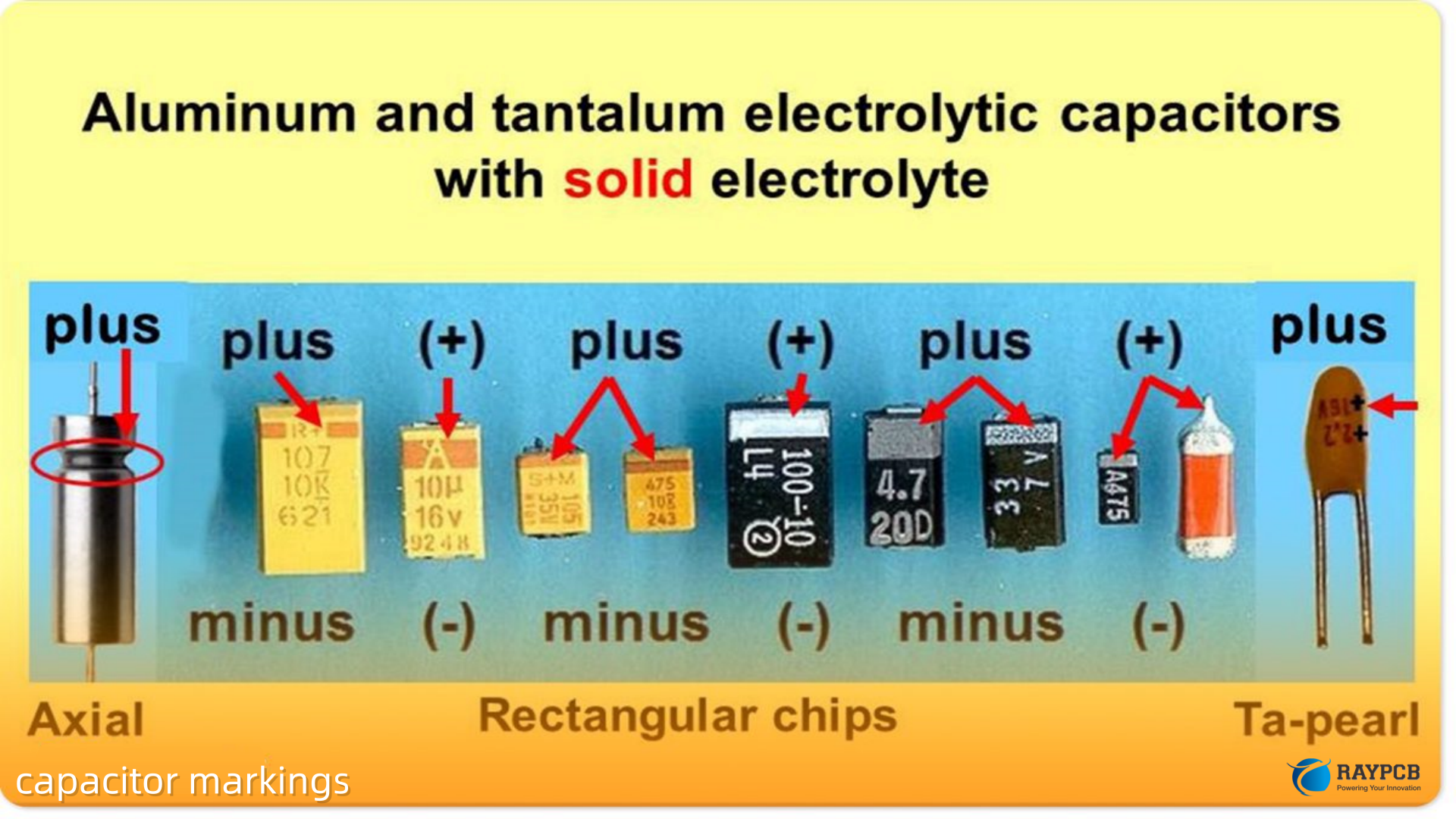
Polarity stripe
White/light stripe on body
Indicates negative terminal
Longer lead
Positive lead
Anode (+)
Shorter lead
Negative lead
Cathode (−)
The negative stripe runs the full height of the can and is clearly visible. On PCBs, the silkscreen will show a “+” marker for the positive pad. Always cross-reference both.
Film Capacitor Markings
Film capacitors follow a similar convention to ceramics but are large enough to print readable values. You’ll see markings like 0.1µF 250V or 100nF 63V. The voltage rating on film caps tends to be high — they’re often used in mains-connected circuits.
How to Read Capacitor Markings on Ceramic Capacitors
This is where things get technical. Small ceramic capacitors — especially SMD types — have almost no room for printing, so they use compact code systems.
The 3-Digit Capacitance Code (EIA Standard)
The most widely used ceramic capacitor marking system uses a 3-digit number. The result is always expressed in picofarads (pF).
Rule: First two digits = significant figures. Third digit = number of zeros (multiplier).
3-Digit Capacitor Code Chart
Marking Code
Calculation
Value in pF
Converted Value
010
01 × 10⁰
1 pF
1 pF
100
10 × 10⁰
10 pF
10 pF
101
10 × 10¹
100 pF
100 pF
102
10 × 10²
1,000 pF
1 nF
103
10 × 10³
10,000 pF
10 nF / 0.01 µF
104
10 × 10⁴
100,000 pF
100 nF / 0.1 µF
105
10 × 10⁵
1,000,000 pF
1 µF
220
22 × 10⁰
22 pF
22 pF
221
22 × 10¹
220 pF
220 pF
472
47 × 10²
4,700 pF
4.7 nF
683
68 × 10³
68,000 pF
68 nF
334
33 × 10⁴
330,000 pF
330 nF
Special case — the “9” multiplier: When the third digit is 9, it means × 0.1. So “229” = 22 × 0.1 = 2.2 pF.
Tolerance Code Letters on Ceramic Capacitors
After the 3-digit value code, a single letter indicates the tolerance — how close the actual capacitance is to the marked value:
Letter Code
Tolerance
Use Case
A
±0.05 pF
Ultra-precision RF
B
±0.1 pF
Precision RF, oscillators
C
±0.25 pF
RF matching
D
±0.5 pF
High-precision circuits
F
±1%
Precision filters, timing
G
±2%
General precision
J
±5%
Standard signal circuits
K
±10%
General purpose bypass
M
±20%
Power supply decoupling
Z
+80% / −20%
Non-critical bulk use
For an IC decoupling application, K or M is fine. For a crystal oscillator load capacitor or an active filter, you need F or better.
Voltage Rating Codes on Ceramic Capacitors
When space allows, a letter or number-letter code indicates the voltage rating:
Code
Voltage Rating
0G
4 V
0J
6.3 V
1A
10 V
1C
16 V
1E
25 V
1H
50 V
1J
63 V
2A
100 V
2D
200 V
2E
250 V
2H
500 V
3A
1000 V
On many small SMD ceramics (0402, 0201), voltage and tolerance codes are omitted entirely due to space constraints — you have to check the reel label or datasheet.
Temperature Coefficient Codes — The Dielectric Identifier
One of the most important (and most overlooked) capacitor markings is the temperature coefficient code. This tells you what dielectric material is used and how the capacitance will behave across temperature.
EIA Temperature Coefficient Codes for Ceramic Capacitors
Code
Also Known As
Temp Range
Capacitance Change
Best Use
C0G
NP0
−55°C to +125°C
±30 ppm/°C (virtually zero)
RF, oscillators, precision timing
X5R
—
−55°C to +85°C
±15%
General SMD decoupling
X7R
—
−55°C to +125°C
±15%
Wide-temp decoupling, filtering
X8R
—
−55°C to +150°C
±15%
High-temp automotive
Y5V
—
−30°C to +85°C
+22% / −82%
Non-critical bypass only
Z5U
—
+10°C to +85°C
+22% / −56%
Older designs, avoid for new work
This is the marking that trips up engineers most often. A Y5V capacitor can lose over 80% of its rated capacitance at temperature extremes or under DC bias. If your schematic calls for 10µF X7R and you substitute Y5V “because it’s the same value,” the circuit may not work correctly in real conditions.
Decoding the EIA temperature code system:
The code uses a three-part structure. For X7R as an example:
X = lower temperature limit (−55°C)
7 = upper temperature limit (125°C)
R = maximum capacitance change (±15%)
First Letter
Lower Temp Limit
X
−55°C
Y
−30°C
Z
+10°C
Middle Number
Upper Temp Limit
2
+45°C
4
+65°C
5
+85°C
6
+105°C
7
+125°C
8
+150°C
9
+200°C
Last Letter
Max Capacitance Change
P
±10%
R
±15%
S
±22%
T
+22% / −33%
U
+22% / −56%
V
+22% / −82%
Tantalum Capacitor Markings
Tantalum capacitors are polarized and have their own marking convention. Most through-hole tantalum caps print the value directly (e.g., 4.7µF 16V) with a “+” marking on the positive lead.
SMD tantalum caps (the small rectangular ones with a stripe at one end) follow this convention:
Marking Element
Description
Stripe / band
Indicates the POSITIVE terminal (opposite to electrolytic convention — don’t confuse them)
Value code
Printed value in µF
Voltage code
Letter or number-letter system similar to ceramics
This is a critical difference to remember: on electrolytic caps, the stripe marks the negative terminal. On tantalum SMD caps, the stripe marks the positive terminal. Mixing this up is one of the most common capacitor polarity mistakes in SMD rework.
SMD Capacitor Package Sizes and What They Tell You
SMD capacitors don’t always have visible markings, but the package size itself communicates usable capacitance ranges:
Package Code
Dimensions (mm)
Typical Capacitance Range
Typical Use
0201
0.6 × 0.3
1 pF – 100 nF
High-density RF, mobile
0402
1.0 × 0.5
1 pF – 10 µF
General SMD, decoupling
0603
1.6 × 0.8
1 pF – 22 µF
Standard SMD design
0805
2.0 × 1.25
1 pF – 47 µF
Higher capacitance SMD
1206
3.2 × 1.6
100 pF – 100 µF
High capacitance, power
1210
3.2 × 2.5
1 nF – 100 µF
High voltage / high cap
1812
4.5 × 3.2
1 nF – 100 µF
High voltage safety caps
When a ceramic cap has no printed marking at all — which happens frequently on 0201 and 0402 parts — your only way to identify it is from the reel label, the BOM, or by measuring with an LCR meter.
Frequently Asked Questions About Capacitor Markings
1. What does “104” mean on a ceramic capacitor?
The code “104” means 10 followed by 4 zeros in picofarads: 100,000 pF, which equals 100 nF or 0.1µF. This is the single most common decoupling capacitor value in digital electronics. You’ll see it on SMD ceramics and through-hole discs alike. The calculation is always: first two digits (10) × 10 to the power of the third digit (10⁴) = 100,000 pF.
2. How do I tell the positive from negative terminal on a capacitor?
On through-hole electrolytic capacitors, the longer lead is positive and the can usually has a stripe marking the negative terminal. On SMD electrolytic caps, look for the “−” marking or stripe on the negative side. On SMD tantalum capacitors, the stripe or band marks the positive terminal — the opposite convention from electrolytics. Non-polarized types like ceramic and film caps have no polarity and can be connected either way.
3. What does X7R mean on a capacitor?
X7R is a temperature coefficient code for ceramic capacitors. It means the capacitor operates from −55°C (X) to +125°C (7) with a maximum capacitance change of ±15% (R) across that range. It’s a general-purpose dielectric — better stability than Y5V/Z5U but not as precise as C0G/NP0. X7R is the most commonly specified dielectric for bypass and decoupling caps in commercial electronics.
4. Why do some SMD capacitors have no markings at all?
Very small SMD capacitors — particularly 0201 and 0402 package sizes — are often left blank because there simply isn’t enough surface area to print readable characters. The component identity is carried on the reel label and in the BOM. If you’ve lost track of a blank SMD capacitor, your only option is to measure it with an LCR meter and cross-reference the value with your design documentation.
5. What does the voltage rating on a capacitor marking mean, and can I use a higher-rated cap?
The voltage rating is the maximum DC voltage the capacitor can safely handle across its terminals. Exceeding it risks dielectric breakdown and component failure. Using a higher-rated capacitor is generally safe and often recommended — a 50V-rated cap in a 12V circuit has more headroom and will typically last longer. Just verify that the physical size fits your footprint and that the capacitance value hasn’t shifted significantly due to the dielectric characteristics of the higher-voltage part.
Final Thoughts on Reading Capacitor Markings
Capacitor markings are a compact but information-dense system once you understand the rules. The 3-digit code gives you the value, the tolerance letter tells you accuracy, the voltage code sets your operating limit, and the temperature coefficient code (especially for ceramics) tells you how the component will behave across the real operating range of your product.
The polarity distinction between electrolytic and tantalum SMD caps is the one that bites engineers most often on rework — so print out that reference table and keep it at your workbench. The few minutes spent learning to decode these markings will save you hours of troubleshooting bad boards.
If you’ve ever touched a live PCB and felt a mild zap even after unplugging it, you’ve already had a very personal introduction to how a capacitor works. As a PCB engineer, capacitors are probably the components I interact with most — and yet they’re still one of the most misunderstood passives on any board. This guide breaks down how does a capacitor work, from the basic physics of charge storage to the practical discharge curves you need to understand when designing real circuits.
What Is a Capacitor? (And Why Should You Care)
A capacitor is a passive two-terminal electrical component that stores energy in an electric field. Unlike a battery, which stores energy chemically, a capacitor stores it electrostatically — and it can release that energy almost instantaneously. That’s what makes it so useful for decoupling, filtering, and energy buffering on a PCB.
At its most basic, a capacitor consists of:
Two conductive plates (typically metal)
A dielectric material between them (insulating layer)
Two terminals connecting to the plates
The dielectric is key. It prevents current from flowing directly between the plates but allows an electric field to build up across them. The type of dielectric used — ceramic, electrolytic, film, tantalum — determines most of the capacitor’s electrical characteristics.
If you want to understand how a capacitor behaves on a PCB, you first need to understand what’s happening at the atomic level between those two plates.
The Physics Behind How a Capacitor Works
How Electric Charge Builds Up on the Plates
When you connect a capacitor to a voltage source, electrons from the negative terminal of the source are pushed onto one plate. This makes that plate negatively charged. Simultaneously, electrons are pulled away from the other plate, leaving it positively charged.
Here’s the counterintuitive part: no current actually flows through the dielectric. The charge just accumulates on the plates. The electric field created between them is what stores the energy.
The relationship between charge, capacitance, and voltage is expressed in one of the most fundamental equations in electronics:
Q = C × V
Where:
Q = charge stored (coulombs)
C = capacitance (farads)
V = voltage across the capacitor (volts)
This equation tells you something very practical: a larger capacitance means you can store more charge at the same voltage. Double the capacitance, double the stored charge.
What Is an Electric Field Inside a Capacitor?
An electric field is a region where an electric force acts on charged particles. Inside a capacitor, the electric field points from the positive plate to the negative plate and is (ideally) uniform across the gap.
The strength of this electric field is:
E = V / d
Where d is the distance between the plates. This is why reducing the gap between plates increases the electric field strength — and also why dielectric breakdown is a real failure mode if you exceed a capacitor’s voltage rating.
The energy stored in this electric field is given by:
W = ½ × C × V²
Notice the V² term. That means if you double the voltage, you quadruple the stored energy. This is exactly why high-voltage capacitors in power supplies can be genuinely dangerous even when the circuit is off.
Capacitance: What Determines It?
Capacitance isn’t arbitrary — it’s determined by three physical factors:
Factor
Effect on Capacitance
Engineer’s Takeaway
Plate area (A)
Larger area = higher capacitance
Bigger footprint = more capacitance
Plate separation (d)
Smaller gap = higher capacitance
Thin dielectrics give high values
Dielectric constant (εr)
Higher εr = higher capacitance
Material choice drives performance
The formula is:
C = ε₀ × εr × A / d
Where ε₀ is the permittivity of free space (8.854 × 10⁻¹² F/m).
This formula is what separates a 10pF ceramic cap from a 1000µF electrolytic. The electrolytic achieves its massive capacitance by using an extremely thin oxide layer as the dielectric (tiny d) and having an enormous effective plate area through a rolled foil construction.
How Does a Capacitor Charge? The RC Time Constant
When you connect a capacitor in series with a resistor to a DC voltage source, it doesn’t charge instantly. The charging follows an exponential curve governed by the RC time constant.
The Charging Equation
V(t) = V_source × (1 – e^(-t/RC))
Where:
R = resistance in ohms
C = capacitance in farads
RC = the time constant (τ, tau) in seconds
t = time elapsed
The time constant τ = RC is the time it takes the capacitor to charge to approximately 63.2% of the supply voltage.
RC Charging Table
Time Elapsed
Voltage (% of V_source)
Charge Status
1τ (1 × RC)
63.2%
Charging fast
2τ
86.5%
Slowing down
3τ
95.0%
Nearly there
4τ
98.2%
Almost full
5τ
99.3%
Considered fully charged
In practice, PCB designers treat 5τ as “fully charged.” For a 10kΩ resistor and 100µF capacitor: τ = 1 second, so the cap is fully charged in about 5 seconds.
Why Doesn’t the Current Stay Constant During Charging?
At the moment you apply voltage, the capacitor looks like a short circuit — current rushes in at its maximum rate (limited only by R). As charge builds up, the voltage across the capacitor opposes the source voltage, reducing the current. Eventually, the capacitor voltage equals the source voltage, and current drops to zero. This is exactly why capacitors block DC in steady state but allow transient current during switching events.
How Does a Capacitor Discharge?
Discharge is just the reverse process. If you remove the voltage source and connect the charged capacitor through a resistor, the stored energy is released.
The Discharge Equation
V(t) = V₀ × e^(-t/RC)
Where V₀ is the initial voltage across the capacitor.
RC Discharging Table
Time Elapsed
Voltage (% of V₀)
Energy Remaining
1τ
36.8%
~13.5%
2τ
13.5%
~1.8%
3τ
5.0%
~0.25%
4τ
1.8%
~0.03%
5τ
0.7%
~0.005%
Notice how the energy drops much faster than the voltage — that’s because energy scales with V². This is an important design consideration when sizing bulk capacitors for hold-up circuits in power supplies.
Capacitors in AC vs. DC Circuits
Capacitors Block DC, Pass AC — Here’s Why
In a DC circuit, once a capacitor is fully charged, current stops flowing. The capacitor essentially acts as an open circuit. This is why capacitors are used as coupling components — they block DC bias while passing the AC signal riding on top of it.
In an AC circuit, the voltage is constantly changing, so the capacitor is always charging and discharging. Current appears to “flow through” the capacitor. The opposition to this current flow is called capacitive reactance:
Xc = 1 / (2π × f × C)
Where f is frequency in Hz.
Capacitive Reactance vs. Frequency
Frequency
Xc (for 100nF cap)
Practical Meaning
10 Hz
159,155 Ω
Blocks audio sub-bass
1 kHz
1,592 Ω
Partial pass
100 kHz
15.9 Ω
Good bypass cap
10 MHz
0.159 Ω
Near short circuit
1 GHz
0.0016 Ω
RF bypass
This is why decoupling capacitors need to be selected based on the switching frequency of your IC — not just slapped on arbitrarily.
Types of Capacitors and How Their Construction Affects Behavior
Understanding the internal construction of each type helps you make better choices on a PCB.
Ceramic Capacitors (MLCC)
Multi-layer ceramic capacitors (MLCCs) stack hundreds of alternating dielectric and electrode layers to achieve high capacitance in a tiny package. They have excellent high-frequency performance and low ESR (equivalent series resistance), making them the go-to decoupling cap on most PCBs.
Watch out for: Capacitance drop with DC bias voltage. A 10µF X5R MLCC rated at 10V might only deliver 3–4µF when biased at 9V. Always check the derating curve in the datasheet.
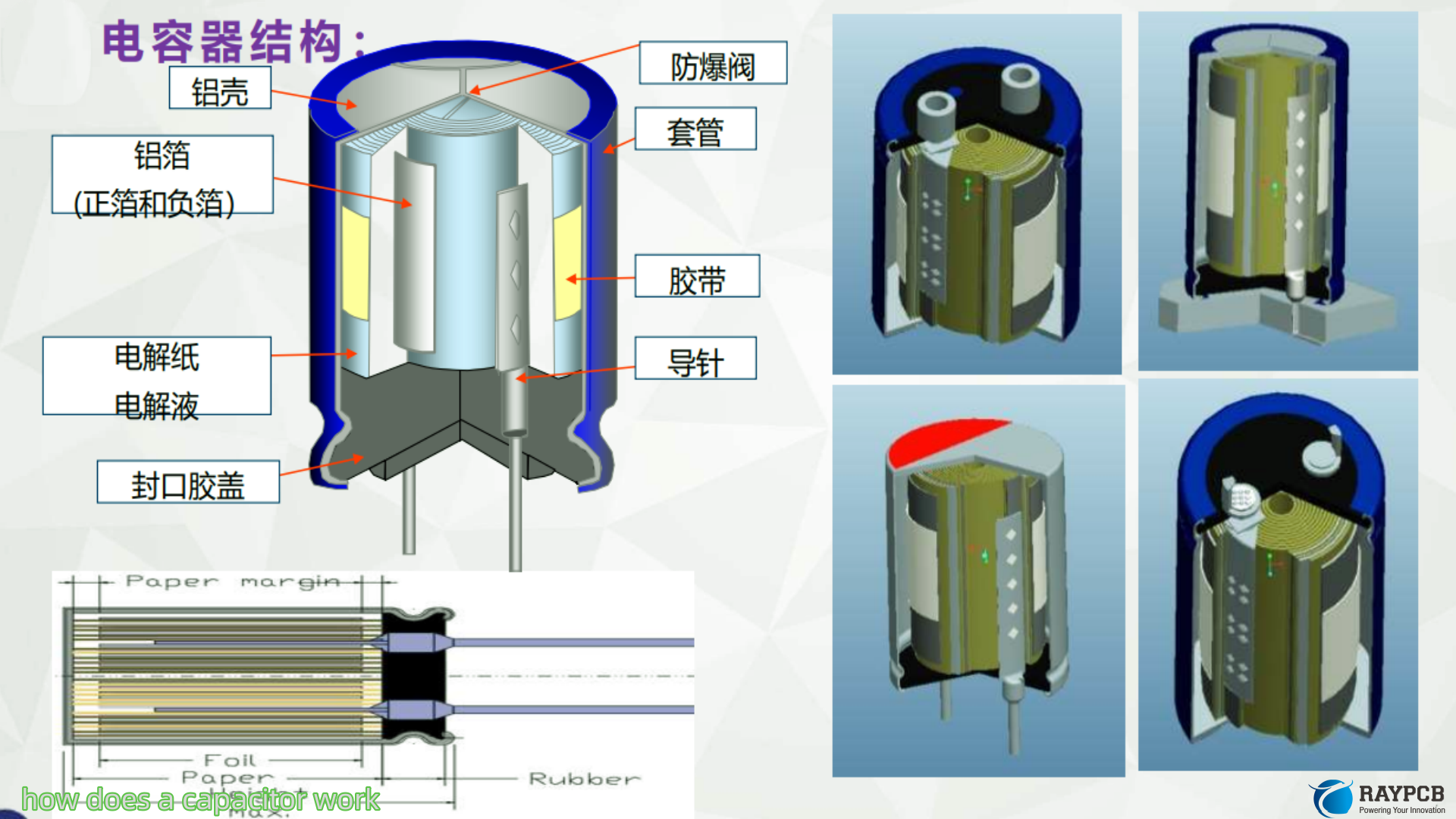
Electrolytic Capacitors (Aluminum)
These use a wound aluminum foil with an extremely thin aluminum oxide dielectric. They achieve very high capacitance values (up to tens of thousands of µF) but are polarized — connect them backwards and they will fail, sometimes spectacularly.
Watch out for: High ESR at high frequencies, limited lifetime (especially at elevated temperatures), and polarity. These are bulk storage and power-line filtering caps, not high-frequency decouplers.
Tantalum Capacitors
Tantalum caps offer better volumetric efficiency than aluminum electrolytics and lower ESR. But they’re infamous for failing short-circuit when exposed to voltage spikes — which can cause board fires in extreme cases.
Watch out for: Always derate tantalum caps to 50% of their rated voltage for reliable operation. Never use them in inrush-prone environments without protection.
Film Capacitors
Polyester or polypropylene film caps are prized for their stability, low distortion, and predictable behavior over temperature. They’re common in analog audio, precision timing, and power factor correction circuits.
Capacitor Type Comparison Table
Type
Capacitance Range
Polarity
ESR
Best For
MLCC Ceramic
1pF – 100µF
Non-polar
Very low
Decoupling, RF, signal
Aluminum Electrolytic
1µF – 100,000µF
Polar
Medium-High
Bulk storage, PSU filter
Tantalum
0.1µF – 2,200µF
Polar
Low
Compact power filtering
Film
100pF – 100µF
Non-polar
Low
Audio, timing, precision
Supercapacitor
0.1F – 3,000F
Polar
Very low
Energy storage, backup
Capacitor Parameters Every PCB Engineer Must Know
When selecting a capacitor for your design, the part number is just the beginning. These are the parameters that actually matter:
Capacitance (C): Nominal value in farads. Always verify against the derating curves.
Voltage Rating (V_rated): The maximum voltage the dielectric can withstand before breakdown. Always derate — typically 80% for ceramics, 50% for tantalums.
ESR (Equivalent Series Resistance): The resistive loss inside the capacitor. High ESR means more heat generated during ripple current, and reduced effectiveness as a decoupling cap.
ESL (Equivalent Series Inductance): Every capacitor has parasitic inductance. Above the self-resonant frequency (SRF), the cap starts behaving like an inductor. For a 100nF MLCC, this might be at 50–100 MHz.
Temperature Coefficient: Ceramic caps are classified by their temperature behavior — C0G/NP0 caps are ultra-stable, X7R caps drift ±15%, and Y5V caps can shift by -80% at temperature extremes.
Ripple Current Rating: Especially important for electrolytic caps in power supplies. Exceeding the ripple current spec is one of the leading causes of premature electrolytic failure.
Practical Applications: Where Capacitors Actually Earn Their Place
Decoupling and Bypass Capacitors
Every digital IC on a PCB needs decoupling capacitors placed as close to the power pins as physically possible. When the IC switches, it draws a sharp spike of current. The decoupling cap supplies this current locally, preventing the spike from propagating through the power plane as noise.
Typical strategy: 100nF MLCC per IC for high-frequency decoupling, with a 10µF bulk ceramic nearby.
Power Supply Filtering
The ripple on a rectified DC supply is smoothed by a large electrolytic capacitor. The larger the capacitance, the lower the ripple. But there’s a trade point — larger caps mean more inrush current at startup.
RC Timing Circuits and Oscillators
The predictable RC time constant makes capacitors essential in timing circuits — from simple 555 timer configurations to precision crystal oscillator load capacitors.
Signal Coupling and DC Blocking
In analog circuits, a series capacitor passes the AC signal between stages while blocking any DC offset. This prevents the bias point of one stage from disturbing the next.
Snubber Circuits
In switching power supplies and motor drives, RC snubbers (a resistor and capacitor in series across a switch) absorb the energy from voltage spikes caused by parasitic inductance during turn-off. Without them, these spikes can exceed the switch’s voltage rating and cause failures.
Common Capacitor Failures and What Causes Them
ailure Mode
Root Cause
How to Prevent
Dielectric breakdown
Overvoltage or voltage spike
Derate voltage rating
Electrolytic dry-out
Heat over time
Operate below temp rating
Tantalum short circuit
Voltage spike, insufficient derating
50% voltage derating
MLCC crack
PCB flexing, thermal shock
Use flex-crack resistant footprints
Capacitance loss
DC bias effect (MLCC)
Check derating curves at operating voltage
ESR degradation
Age, high ripple current
Select adequate ripple current rating
Useful Resources for Further Reading
Here are some authoritative references that are worth bookmarking:
TDK MLCC Product Catalog & White Papers:product.tdk.com — excellent application notes on DC bias derating
Kemet SPICE Models & Parametric Search:kemet.com — download SPICE models for accurate simulation
IPC-2221B Standard (Generic Standard on Printed Board Design): Available via ipc.org — PCB design rules including component placement guidelines
Würth Elektronik Application Notes:we-online.com — free downloadable guides on passive component selection for EMC
All About Circuits (Reference):allaboutcircuits.com — well-structured textbook-style reference for RC circuit theory
Frequently Asked Questions About How Capacitors Work
1. Does current actually flow through a capacitor?
Not in the conventional sense — electrons don’t physically cross the dielectric. What happens is that electrons accumulate on one plate and are simultaneously repelled from the other plate. In AC circuits, this continuous charge/discharge cycle produces a displacement current that makes it appear as though current is flowing through the capacitor.
2. Why does a capacitor block DC but pass AC?
In DC steady state, the capacitor charges up to the supply voltage and then current stops — effectively an open circuit. In AC, the voltage constantly reverses, so the capacitor never fully charges in one direction. It continuously charges and discharges, allowing current to flow through the circuit.
3. What happens if you exceed a capacitor’s voltage rating?
The dielectric breaks down. For ceramics and films, this usually means a permanent short circuit. For electrolytics, it can result in venting, bulging, or in worst cases, an explosion. Always derate your voltage ratings — I personally never run a ceramic cap above 80% of its rated voltage in a production design.
4. Why do electrolytic capacitors have polarity?
The dielectric of an electrolytic capacitor is a very thin layer of aluminum oxide, formed electrochemically on the surface of the aluminum foil. This oxide layer is directional — it acts as a dielectric only when the anode (positive terminal) is at a higher potential than the cathode. Reverse the polarity and the oxide layer dissolves, shorting the cap. The resulting current causes rapid heating, gas buildup, and failure.
5. What is the self-resonant frequency (SRF) of a capacitor, and why does it matter?
Every real capacitor has parasitic inductance (ESL) from its leads and internal construction. At the SRF, the capacitive reactance equals the inductive reactance and they cancel — the cap looks like a pure resistor (ESR). Above the SRF, the cap actually behaves inductively. This is critical for high-speed PCB design: a 100nF decoupling cap might have an SRF of 50 MHz. Above that frequency, it’s no longer decoupling — it’s actually adding inductance to your power rail. That’s why high-speed designs use multiple cap values in parallel to extend the effective decoupling bandwidth.
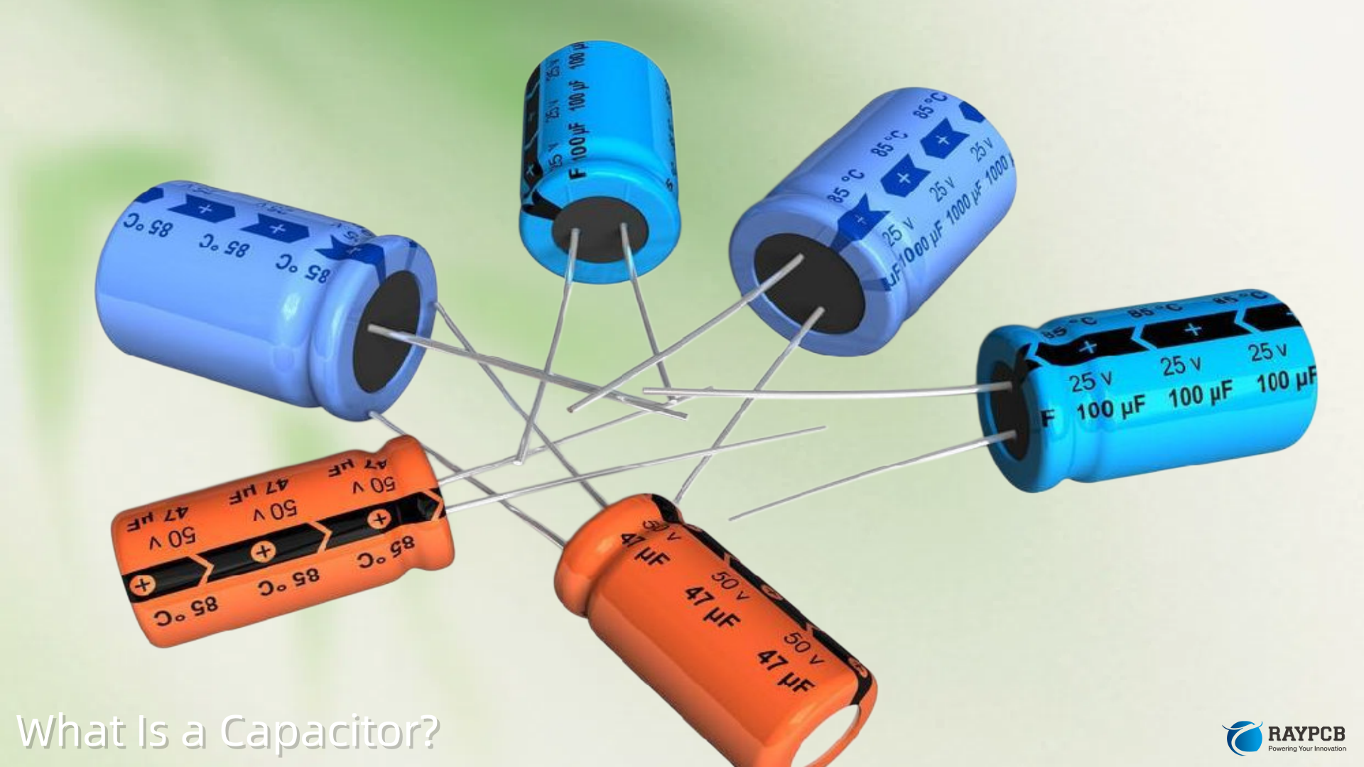
If you’ve ever opened up a circuit board or watched an electronics tutorial, you’ve almost certainly come across a capacitor. They’re everywhere — from the tiniest wearable devices to massive industrial power systems. Yet for many beginners (and even some seasoned hobbyists), the question what is a capacitor remains surprisingly fuzzy.
As a PCB engineer, I get asked this more than almost anything else. So let me walk you through everything you need to know about capacitors — how they work, what types exist, how to read them, and how to use them correctly on a PCB. No unnecessary jargon. Just clear, practical knowledge.
What Is a Capacitor?
A capacitor is a passive electronic component that stores and releases electrical energy in the form of an electric field. Think of it like a tiny, fast-charging rechargeable battery — but instead of using a chemical reaction, it stores energy between two conductive plates separated by an insulating material called a dielectric.
The fundamental job of a capacitor is to hold a charge temporarily and release it when needed. This makes it incredibly useful for smoothing power supplies, filtering signals, timing circuits, and coupling AC signals while blocking DC.
Every capacitor on a PCB plays a specific functional role — and understanding that role is the first step to becoming a confident circuit designer.
How Does a Capacitor Work?
The Basic Operating Principle
At its core, a capacitor consists of two conductive plates (usually made of metal) placed very close together but not touching. Between them sits the dielectric — an insulating material that prevents direct current from flowing through but allows an electric field to build up.
When you apply a voltage across the capacitor’s terminals:
Electrons accumulate on one plate (negative charge)
The opposite plate loses electrons (positive charge)
An electric field forms between the two plates
Energy is stored in that field
When the voltage source is removed or a load is connected, the capacitor discharges — releasing that stored energy back into the circuit.
The Charging and Discharging Curve
Capacitors don’t charge or discharge instantly. They follow an exponential curve described by the RC time constant (τ = R × C), where R is the resistance in the circuit and C is the capacitance. After one time constant, a capacitor charges to about 63.2% of the supply voltage. After five time constants, it’s considered fully charged (~99.3%).
This behavior is exactly what makes capacitors so useful in timing circuits and filters.
Capacitance: The Key Measurement
What Is Capacitance?
Capacitance is the measure of a capacitor’s ability to store charge per unit of voltage. It is measured in Farads (F), named after physicist Michael Faraday.
In practice, most capacitors you’ll work with are measured in smaller units:
Unit
Symbol
Equivalent
Microfarad
µF
10⁻⁶ F
Nanofarad
nF
10⁻⁹ F
Picofarad
pF
10⁻¹² F
Millifarad
mF
10⁻³ F
Surface mount capacitors on a PCB often range from a few picofarads to several hundred microfarads, depending on their application.
What Affects Capacitance?
The capacitance of a capacitor depends on three physical factors:
Factor
Effect on Capacitance
Plate area (A)
Larger plates = higher capacitance
Distance between plates (d)
Smaller gap = higher capacitance
Dielectric material (ε)
Higher permittivity = higher capacitance
This relationship is expressed as: C = ε × (A / d)
Types of Capacitors
One of the most common areas of confusion for beginners is the sheer variety of capacitor types. Each type has its own characteristics, strengths, and ideal use cases. Here’s a comprehensive breakdown.
Ceramic Capacitors
Ceramic capacitors are the most widely used type in modern PCB design. They use a ceramic material as the dielectric and are available in a huge range of values from a few picofarads to tens of microfarads.
Key characteristics:
Non-polarized (can be connected either way)
Very low ESR (Equivalent Series Resistance)
Available in SMD packages (0201, 0402, 0603, 0805, etc.)
Temperature stability varies by class (C0G/NP0 most stable, X5R/X7R good for general use, Y5V poorest stability)
Best for: Decoupling/bypass capacitors, high-frequency filtering, general-purpose signal filtering
Electrolytic Capacitors
Electrolytic capacitors use an electrolyte solution to achieve very high capacitance values — often from 1 µF up to tens of thousands of µF. They are polarized, meaning they must be connected with the correct polarity or they can fail catastrophically.
Key characteristics:
Polarized (has a positive and negative terminal)
Higher ESR than ceramics
Available in through-hole and SMD versions
Shorter lifespan at high temperatures
Best for: Power supply filtering, bulk energy storage, audio coupling stages
Tantalum Capacitors
Tantalum capacitors offer a middle ground — higher capacitance density than ceramics but lower ESR and smaller size than electrolytics. They are also polarized.
Key characteristics:
Polarized
Compact and reliable
Sensitive to voltage spikes (can fail short if over-volted)
More expensive than ceramics or electrolytics
Best for: Portable electronics, medical devices, power supply decoupling where space is critical
Film Capacitors
Film capacitors use a thin plastic film as the dielectric. They are highly stable and have very low ESR and ESL (Equivalent Series Inductance).
Key characteristics:
Non-polarized
Excellent temperature stability
Low self-heating
Physically larger than other types
Best for: Audio circuits, precision timing, power factor correction, motor run capacitors
Supercapacitors (Ultracapacitors)
Supercapacitors are a class apart. They can store dramatically more energy than conventional capacitors — sometimes hundreds or thousands of farads — by using an electrochemical double-layer effect.
Key characteristics:
Very high capacitance (1F to 3000F+)
Low energy density compared to batteries, but much faster charge/discharge
Limited voltage rating (typically 2.5–2.7V per cell)
Best for: Energy harvesting, backup power systems, regenerative braking, IoT devices that need brief power bursts
Capacitor Type Comparison Table
Type
Capacitance Range
Polarized?
ESR
Typical Use
Ceramic (C0G)
1pF – 1µF
No
Very Low
RF, precision
Ceramic (X7R)
100pF – 10µF
No
Low
Decoupling
Electrolytic
1µF – 100,000µF
Yes
Medium-High
Power filtering
Tantalum
0.1µF – 2,200µF
Yes
Low
Portable electronics
Film
1nF – 100µF
No
Very Low
Audio, precision
Supercapacitor
0.1F – 3,000F
Yes
Very Low
Energy storage
How to Read Capacitor Values
Reading Through-Hole Capacitors
Most electrolytic capacitors are straightforward — the value is printed directly on the body (e.g., “100µF 25V”). The longer lead is positive (+), and many have a stripe indicating the negative terminal.
Reading Ceramic Capacitor Codes
SMD and small ceramic capacitors often use a 3-digit code. Here’s how to decode it:
The first two digits are the significant figures
The third digit is the multiplier (number of zeros to add)
The result is in picofarads (pF)
Example:
Code
Calculation
Value
104
10 × 10⁴
100,000 pF = 100 nF = 0.1 µF
103
10 × 10³
10,000 pF = 10 nF
472
47 × 10²
4,700 pF = 4.7 nF
220
22 × 10⁰
22 pF
Voltage Rating
Every capacitor has a voltage rating — the maximum voltage it can safely handle. As a PCB engineer, I always recommend using a capacitor rated at at least 1.5× to 2× the maximum voltage it will see in the circuit. This provides a safety margin against voltage spikes and extends component life.
What Does a Capacitor Do in a Circuit?
Understanding what a capacitor actually does in different circuit contexts will save you hours of debugging. Here are the most common roles:
1. Decoupling / Bypass Capacitor
This is probably the most common use of a capacitor on a PCB. A small ceramic capacitor (typically 100nF) placed close to an IC’s power pin “decouples” it from the rest of the power supply. When the IC suddenly draws a burst of current, the capacitor supplies that current instantly — preventing a voltage dip that could cause logic errors or noise.
2. Bulk Capacitance
Larger electrolytic or tantalum capacitors are placed across power rails to handle slower, larger current demands. Where decoupling caps handle high-frequency transients, bulk caps handle lower-frequency demand changes — like when a motor starts or a display lights up.
3. Filtering
Capacitors are fundamental building blocks in filter circuits:
Filter Type
What It Does
Low-pass filter
Passes low frequencies, blocks high frequencies
High-pass filter
Passes high frequencies, blocks low frequencies
Band-pass filter
Passes a specific frequency range
Notch filter
Rejects a specific frequency
A simple low-pass RC filter uses a resistor and capacitor in series, taking the output across the capacitor. The cutoff frequency is: f = 1 / (2π × R × C)
4. Coupling / DC Blocking
In audio and RF circuits, a capacitor in series with a signal path passes AC (the audio or RF signal) while blocking DC offset. This is called AC coupling and is essential for connecting circuit stages with different DC bias levels.
5. Timing
In a classic 555 timer circuit, the time delay or oscillation frequency is set by an RC network. The capacitor charges and discharges through a resistor to create a predictable timing interval.
6. Energy Storage
In camera flash circuits, camera sensors, and power backup systems, capacitors store charge and then release it rapidly when needed. A camera flash is a perfect example — the capacitor charges slowly from a small battery, then dumps that energy almost instantly through the flash tube.
Capacitor Specifications You Need to Understand
Before you select a capacitor for your design, you need to understand these key specifications:
Specification
Description
Why It Matters
Capacitance (C)
Value in pF, nF, or µF
Determines the function in circuit
Voltage rating (V)
Max operating voltage
Exceeding it damages/destroys the cap
Tolerance
Accuracy of capacitance (±5%, ±10%, ±20%)
Critical in precision circuits
ESR
Equivalent Series Resistance
Affects efficiency and heat generation
ESL
Equivalent Series Inductance
Limits high-frequency performance
Temperature coefficient
How much capacitance shifts with temperature
Critical in timing and RF circuits
Leakage current
Small current through dielectric
Matters in low-power and precision circuits
Lifetime / MTBF
Expected service life
Key for reliability engineering
Capacitors in Series and Parallel
Capacitors in Parallel
When capacitors are in parallel, their capacitances add together:
C_total = C1 + C2 + C3 + …
This is useful when you need a higher capacitance value but only have smaller caps available, or when you want to combine a bulk cap with a decoupling cap for wider frequency coverage.
Capacitors in Series
When capacitors are in series, the total capacitance decreases and follows this formula:
1/C_total = 1/C1 + 1/C2 + 1/C3 + …
For two equal capacitors in series: C_total = C/2
Series configurations are used when you need a higher voltage rating than any single capacitor provides.
How to Test a Capacitor
If you suspect a capacitor has failed, here are the most common testing methods:
Using a Multimeter
Set your multimeter to the capacitance measurement mode (if available) and measure across the capacitor terminals. Compare the reading to the marked value — a significantly different reading indicates a failed component.
For electrolytic caps, you can also do a rough test in resistance mode:
Good capacitor: resistance briefly reads low, then climbs toward infinity
Short circuit: resistance stays near zero
Open circuit: no deflection at all
Using an LCR Meter
An LCR meter gives you capacitance, ESR, and sometimes dissipation factor (D) — a much more thorough test. High ESR in an electrolytic capacitor is a common failure mode and is often missed by a basic multimeter.
Visual Inspection
For through-hole electrolytics, look for:
Bulging or domed tops (sign of internal pressure buildup)
Electrolyte leakage (brown crust around the base)
Cracked or damaged casing
Common Capacitor Failures and How to Avoid Them
Failure Mode
Cause
Prevention
Dielectric breakdown
Exceeded voltage rating
Derate voltage to 50–70% of rating
ESR increase
Age, heat, ripple current
Use proper temp-rated caps, add heat management
Short circuit (tantalum)
Voltage spike
Add inrush current limiting, use 2× derating
Capacitance drift
Temperature extremes
Use C0G/NP0 ceramics for stable applications
Mechanical failure (ceramic)
PCB flex stress
Use softer-termination caps on flexible areas
Capacitors on a PCB: Placement Best Practices
From years of hands-on PCB design, here are the placement rules I follow every time:
Decoupling caps must be placed as close as possible to the IC power pin — ideally within 0.5mm. The connection from pad to via should be as short as possible. A decoupling cap placed 5mm away from the IC provides very little benefit at high frequencies.
For bulk capacitors, placement near the power input connector or the main regulator output is the priority. These are handling lower-frequency energy demands, so exact proximity is less critical than for decoupling.
If you’re working on a high-speed digital design, consider placing a 100nF and a 10nF ceramic in parallel for each IC — the combination covers a wider frequency range than either alone.
Finally, avoid placing large electrolytic capacitors near heat-generating components. Heat is an electrolytic capacitor’s primary enemy — it accelerates electrolyte evaporation and dramatically shortens lifespan.
Useful Resources for Learning More About Capacitors
Here are some authoritative resources to deepen your understanding:
A capacitor is an electronic component that temporarily stores electrical energy as an electric field between two conductive plates. It charges up quickly when connected to a power source and releases that energy when needed. Unlike a battery, it stores energy electrostatically (not chemically), so it can charge and discharge extremely fast.
2. What is the difference between a capacitor and a battery?
Both store energy, but very differently. A battery stores energy chemically and can hold a large amount for a long time but charges and discharges slowly. A capacitor stores energy electrostatically, holds much less energy overall, but can charge and discharge almost instantly. This makes capacitors ideal for filtering, decoupling, and burst-energy applications rather than long-term energy supply.
3. Can I replace a capacitor with a higher capacitance value?
Sometimes, but it depends on the application. In power supply filtering, a higher value often works fine or even better. In timing circuits or filters, changing the capacitance directly changes the time constant or cutoff frequency and can break the circuit’s intended behavior. Always check the circuit design before substituting values.
4. Why do electrolytic capacitors have a polarity?
Electrolytic capacitors are manufactured using an electrochemical process that creates a very thin oxide layer on one metal plate — this layer is the dielectric. This process is directional, which means the component only functions correctly (and safely) when connected with the correct polarity. Reverse-biasing an electrolytic can destroy the oxide layer, cause the capacitor to fail short, and sometimes lead to the capacitor venting or rupturing.
5. What happens if a capacitor is connected incorrectly on a PCB?
For non-polarized capacitors (like ceramics), there’s no polarity concern. For polarized types (electrolytic, tantalum), connecting them backwards can cause immediate or gradual failure. In high-current circuits, an incorrectly connected electrolytic capacitor can build up internal pressure and fail explosively. Always double-check polarity markings on both the component and the PCB silkscreen before powering up.
Final Thoughts
Understanding what a capacitor is and how it works is one of the most foundational skills in electronics. Whether you’re designing your first PCB, debugging a power supply, or just trying to understand why an IC keeps resetting, capacitors are almost always part of the story.
The key takeaways: capacitors store energy in an electric field, their behavior is defined by capacitance (measured in Farads), they come in many types each suited to specific jobs, and their placement on a PCB matters enormously for performance. Get these fundamentals right and you’ll make far fewer mistakes at the design stage — and spend far less time troubleshooting later.
If you want to go deeper into how capacitors are used specifically in PCB layouts, I’d recommend exploring manufacturer application notes and PCB design guidelines from IPC — they’re dense but packed with real-world engineering wisdom.
The ESP8266 has revolutionized the world of Wi-Fi IoT projects, becoming the go-to choice for makers, hobbyists, and professionals alike. This tiny yet powerful esp8266 wifi module has democratized Internet of Things development by providing affordable, reliable Wi-Fi connectivity that was once exclusive to expensive industrial solutions.
Since its introduction by Espressif Systems, the esp wifi chip has sparked an unprecedented boom in DIY smart home projects, environmental monitoring systems, and connected device prototypes. What makes the esp module so compelling is its perfect balance of functionality, affordability, and ease of use – factors that have made it the backbone of countless IoT innovations worldwide.
The ESP8266’s popularity stems from its impressive feature set packed into a compact form factor. With built-in Wi-Fi capabilities, adequate processing power, and multiple GPIO pins, this microcontroller can handle everything from simple sensor readings to complex web server operations. The vibrant ecosystem surrounding the ESP8266 includes popular development boards like the NodeMCU, Wemos D1 Mini, and the compact ESP-01, each designed to make Wi-Fi connectivity accessible to developers of all skill levels.
As IoT continues to reshape industries from agriculture to healthcare, the ESP8266 remains at the forefront of this transformation. Its low power consumption makes it ideal for battery-powered applications, while its robust Wi-Fi performance ensures reliable connectivity in demanding environments. Whether you’re building a smart irrigation system, home security network, or industrial monitoring solution, the ESP8266 provides the foundation for bringing your connected device ideas to life.
The chip’s compatibility with familiar development environments like Arduino IDE has lowered the barrier to entry for IoT development. This accessibility, combined with extensive community support and comprehensive documentation, explains why the ESP8266 continues to be the first choice for Wi-Fi-enabled projects. Even with newer alternatives like the ESP32 available, the ESP8266’s proven reliability and cost-effectiveness ensure its continued relevance in the rapidly evolving IoT landscape.
The ESP8266is a low-cost Wi-Fi microcontroller chip developed by Espressif Systems that has become synonymous with affordable IoT connectivity. At its core, the esp8266ex features a 32-bit Xtensa LX106 processor running at 80MHz (overclockable to 160MHz), coupled with integrated 802.11 b/g/n Wi-Fi capabilities. This combination provides developers with both computational power and wireless connectivity in a single, compact package.
The architecture of the esp8266mod is designed for efficiency and versatility. The chip includes 64KB of instruction RAM, 96KB of data RAM, and external flash memory support ranging from 512KB to 16MB depending on the specific module variant. This memory configuration allows the ESP8266 to run complex applications while maintaining its low-power profile, making it suitable for battery-operated IoT devices that need to operate for months or even years on a single charge.
One common misconception involves the term esp2866, which is actually a typographical error for ESP8266. The correct designation is ESP8266, and various modules like the esp8266 mini variants maintain this naming convention while offering different form factors and pin configurations to suit diverse project requirements.
Espressif Systems introduced the ESP8266 in 2014, initially targeting the Chinese market before its global adoption exploded in 2015. The chip’s development history reflects Espressif’s commitment to democratizing IoT connectivity by providing enterprise-grade Wi-Fi capabilities at consumer-friendly prices. This strategic approach disrupted the embedded Wi-Fi market, which had previously been dominated by expensive solutions from established semiconductor companies.
Understanding the relationship between ESP8266 variants is crucial for selecting the right chip for your project. The esp8285 represents an integrated version of the ESP8266 with 1MB of flash memory built directly into the package, eliminating the need for external flash storage. This integration makes the ESP8285 more compact but less flexible in terms of memory expansion.
The comparison between esp8266 esp32 chips reveals important distinctions for project planning. While the esp32 esp8266 discussion often focuses on the ESP32’s superior processing power and Bluetooth connectivity, the ESP8266 maintains advantages in power efficiency, cost-effectiveness, and proven stability for Wi-Fi-only applications. The ESP32 features dual-core processing and additional peripherals, but these enhancements come with increased power consumption and complexity that may be unnecessary for simpler IoT projects.
The ESP8266’s Wi-Fi implementation supports multiple connection modes, including station mode for connecting to existing networks, access point mode for creating its own network, and a combined mode that enables both simultaneously. This flexibility allows developers to create sophisticated networking topologies, from simple sensor nodes that report to cloud services to mesh networks that can extend Wi-Fi coverage across large areas.
The ESP8266 ecosystem encompasses numerous module variants and development boards, each optimized for specific use cases and project requirements. Understanding these options is essential for selecting the most appropriate hardware for your IoT applications.
ESP-01 and ESP-01S Series
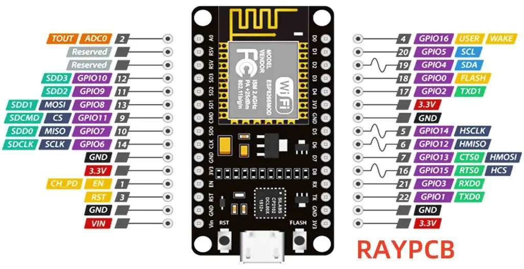
The esp 01 represents the most compact and cost-effective entry point into ESP8266 development. The original esp 01s module features a minimal pin count with only GPIO0, GPIO2, TX, RX, VCC, GND, CH_PD, and RST accessible through its 8-pin header. Despite this limitation, the esp8266 esp 01 has found widespread use in applications where space constraints are paramount and only basic I/O functionality is required.
The esp01s variant improves upon the original design with better antenna performance and more reliable operation. The esp 01 8266 modules are particularly popular for retrofitting existing devices with Wi-Fi connectivity due to their small footprint and low cost. However, developers must work within the constraints of limited GPIO availability, making these modules best suited for simple sensor readings or relay control applications.
ESP-07 and ESP-07S with External Antenna Support
The esp 07 and esp 07s modules address the antenna limitations of smaller variants by providing both onboard ceramic antenna and external antenna connector options. This dual-antenna approach makes these modules ideal for applications requiring extended Wi-Fi range or operation in challenging RF environments. The additional GPIO pins compared to ESP-01 modules provide more flexibility for interfacing with sensors and actuators.
ESP-12 Series: Enhanced GPIO and Flash Memory
The ESP-12 family, including esp 12, esp 12e, and esp 12f variants, represents a significant step up in capability and convenience. The esp8266 12f and esp8266 12e modules feature more accessible GPIO pins, larger onboard flash memory options, and improved antenna designs. These modules strike an excellent balance between functionality and cost, making them popular choices for prototype development and small-scale production.
The ESP-12F variant includes additional improvements in antenna design and pin layout that enhance both performance and ease of use. The extra GPIO pins available on these modules enable more complex projects involving multiple sensors, displays, and communication interfaces without requiring external multiplexers or I/O expanders.
Wemos D1 Series: Arduino-Compatible Form Factors
The wemos d1 mini has achieved legendary status among ESP8266 development boards due to its compact size and Arduino Uno-compatible pin spacing. The wemos d1 mini pro extends this design with additional features like external antenna connector and more robust power regulation. The wemos mini form factor has inspired countless shield designs, creating an ecosystem of stackable modules for rapid prototyping.
The evolution from wemos d1 to wemos d1 r1 and wemos d1 r2 versions reflects continuous improvements in USB connectivity, power management, and build quality. The d1 mini and d1 mini pro variants maintain the popular compact form factor while incorporating lessons learned from earlier designs. The esp d1 mini nomenclature is sometimes used interchangeably with Wemos D1 Mini, reflecting the board’s association with ESP8266 development.
The wemos esp8266 boards have become synonymous with reliable, easy-to-use ESP8266 development platforms. The esp8266 d1 mini format’s popularity has led to numerous compatible boards from various manufacturers, creating a de facto standard for compact ESP8266 development boards.
NodeMCU: The Developer-Friendly Standard
The nodemcu platform revolutionized ESP8266 development by providing a complete development board with USB connectivity, voltage regulation, and breadboard-friendly pin layout. The nodemcu esp8266 boards come in several versions, with nodemcu v3, lolin nodemcu v3, nodemcu amica, and nodemcu v2 being the most common variants. Each version offers slight improvements in layout, components, or build quality while maintaining compatibility with the established NodeMCU pinout.
The nodemcu 8266 designation emphasizes the ESP8266-based nature of these boards, distinguishing them from ESP32-based NodeMCU variants. The node mcu8266 boards have become the de facto standard for ESP8266 education and prototyping due to their plug-and-play nature and extensive documentation.
ESP32-Based Alternatives
While this guide focuses on ESP8266, understanding ESP32 alternatives helps inform hardware selection decisions. The espwroom32 and other esp32 module variants offer increased processing power, Bluetooth connectivity, and more GPIO pins at the cost of higher power consumption and increased complexity.
The node mcu esp 32, node mcu esp32s, node mcu 32s, and esp32 node mcu boards extend the familiar NodeMCU form factor to ESP32 hardware. The esp32 8266 comparison often comes down to project requirements: choose ESP8266 for simple, power-efficient Wi-Fi applications, and ESP32 for projects requiring additional processing power, Bluetooth, or numerous GPIO pins. The wifi esp32 capabilities surpass ESP8266 in raw performance but may be overkill for many IoT applications.
Getting Started: Programming ESP8266 with Arduino IDE
ESP8266 PCB Moudle
Setting up your development environment for ESP8266 programming through Arduino IDE is straightforward and provides access to the familiar Arduino programming model. This approach makes ESP8266 development accessible to anyone with basic Arduino experience while leveraging the extensive Arduino library ecosystem.
Begin by installing the ESP8266 board package in Arduino IDE through the Board Manager. Navigate to File > Preferences and add the ESP8266 board package URL to the Additional Board Manager URLs field. After updating the board manager list, search for “ESP8266” and install the community-maintained package that provides support for various ESP8266 development boards.
The arduino ide nodemcu integration is seamless once the board package is installed. Select your specific board variant from the Tools > Board menu – options include NodeMCU variants, Wemos D1 boards, and generic ESP8266 modules. The esp8266 ide arduino combination provides access to specialized libraries and examples designed specifically for ESP8266 hardware.
Connecting your esp8266 arduino development board varies by model, but most modern boards like NodeMCU and Wemos D1 Mini include USB-to-serial converters for direct computer connection. The arduino esp8266 nodemcu setup requires selecting the correct COM port and upload speed (typically 115200 baud) in the Arduino IDE Tools menu.
Your first project should verify the complete toolchain functionality. Create a simple LED blink program that demonstrates both code compilation and hardware interaction. Most ESP8266 development boards include an onboard LED connected to GPIO2 or GPIO16, making this an ideal starting point for beginners. The familiar Arduino digitalWrite() and delay() functions work identically on ESP8266, easing the transition for Arduino users.
Advanced arduino esp8266 nodemcu programming involves leveraging ESP8266-specific libraries for Wi-Fi connectivity, web server functionality, and cloud integration. The ESP8266WiFi library provides comprehensive network connectivity options, while libraries like ESPAsyncWebServer enable sophisticated web-based interfaces for IoT projects.
The versatility of ESP8266 modules enables an enormous range of IoT projects, from simple sensor monitoring to complex home automation systems. These project examples demonstrate practical applications while highlighting the capabilities that make ESP8266 the preferred choice for Wi-Fi-enabled devices.
Home Automation with Relay Control
Controlling household appliances through Wi-Fi represents one of the most popular ESP8266 applications. The relay module arduino combination with ESP8266 creates powerful automation systems capable of switching high-voltage devices safely. The esp8266 relay interface typically uses a single GPIO pin to control relay coils, while the relay contacts handle the actual load switching.
Simple esp01 relay projects can control individual appliances like lamps or fans, while more complex systems using 8 relay module boards can manage entire rooms or small buildings. These projects often incorporate web-based control interfaces or smartphone app integration for remote operation. Safety considerations are paramount when working with relay-controlled mains voltage systems, requiring proper electrical isolation and protective enclosures.
Wi-Fi Temperature and Environmental Monitoring
Environmental monitoring projects showcase the ESP8266’s ability to collect sensor data and transmit it wirelessly to cloud services or local databases. Temperature and humidity sensors like the DHT22 connect easily to ESP8266 GPIO pins, while the esp8266 wifi connectivity enables regular data uploads to services like ThingSpeak, Blynk, or custom web servers.
These projects often implement deep sleep functionality to extend battery life in remote monitoring applications. The ESP8266’s ultra-low power modes can reduce current consumption to microamperes, enabling months of operation on battery power while still providing regular data updates.
Smart Lighting and Display Projects
LED strip control and OLED display integration represent visually engaging ESP8266 projects that combine connectivity with immediate visual feedback. WS2812B addressable LED strips work excellently with ESP8266 modules, creating colorful lighting effects controllable through web interfaces or smartphone apps. The esp8266 wifi module arduino combination provides the processing power needed for complex lighting animations while maintaining Wi-Fi connectivity for remote control.
OLED display projects often combine local sensor readings with internet-sourced information like weather data or time synchronization. These projects demonstrate the ESP8266’s ability to function as both data collector and information display device, creating self-contained IoT solutions that provide immediate value to users.
Security and Monitoring Applications
IoT security projects leverage the ESP8266’s connectivity for remote monitoring and alert systems. Camera integration using ESP32-CAM modules (which extend ESP8266 concepts) creates wireless security cameras, while door/window sensors connected to ESP8266 modules can send instant notifications when security perimeters are breached.
Motion detection projects using PIR sensors connected to ESP8266 modules demonstrate how simple sensors can create sophisticated monitoring systems. These projects often incorporate email or SMS notifications, showcasing the ESP8266’s ability to integrate with various internet services and APIs.
The esp8266 wifi module arduino architecture excels in these applications due to its balance of processing capability and power efficiency. Security applications often require 24/7 operation while maintaining minimal power consumption, making the ESP8266’s sleep modes and wake-on-interrupt capabilities particularly valuable.
The wifi shield for arduino concept takes on new meaning with ESP8266 modules, as they provide not just connectivity but complete processing capability that can often replace traditional Arduino boards entirely. This integration simplifies project architectures while reducing cost and power consumption compared to separate microcontroller and Wi-Fi shield combinations.
ESP8266 vs. ESP32: Which Should You Choose?
The decision between ESP8266 and ESP32 depends on specific project requirements, with each platform offering distinct advantages for different types of IoT applications. Understanding these differences ensures optimal hardware selection for your development needs.
The ESP8266 excels in applications requiring basic Wi-Fi connectivity with minimal power consumption and cost. Its single-core architecture running at 80MHz provides sufficient processing power for sensor data collection, simple control logic, and web server operations. The ESP8266’s proven stability and extensive community support make it ideal for straightforward IoT projects where reliability and simplicity are priorities.
In contrast, the esp32 module platform offers significantly more processing power with its dual-core Xtensa LX6 processor running at up to 240MHz. The esp32 home automation applications benefit from this additional computational capability when handling multiple simultaneous tasks, complex algorithms, or real-time processing requirements. The ESP32’s Bluetooth Low Energy support adds connectivity options that ESP8266 cannot provide.
Memory differences between platforms significantly impact project capabilities. ESP8266 modules typically include 4MB of flash memory and limited RAM, sufficient for most IoT applications but constraining for data-intensive projects. ESP32 modules generally provide more flash memory options and substantially more RAM, enabling larger programs and more sophisticated data handling.
GPIO availability represents another crucial distinction. ESP8266 modules provide approximately 9-11 usable GPIO pins depending on the specific variant, while ESP32 modules offer 25+ GPIO pins with more diverse functionality including multiple ADC channels, DAC outputs, and specialized communication interfaces. Projects requiring numerous sensors or actuators often necessitate ESP32’s expanded I/O capabilities.
Power consumption patterns differ significantly between platforms. ESP8266 achieves lower deep sleep current consumption, making it superior for battery-powered applications requiring months or years of operation between battery replacements. ESP32’s higher performance comes with increased power requirements, though its advanced power management features can mitigate consumption in optimized applications.
Cost considerations often favor ESP8266 for price-sensitive applications. ESP8266 modules typically cost 30-50% less than equivalent ESP32 modules, making them attractive for large-scale deployments or educational projects with tight budgets. However, the ESP32’s additional capabilities may justify its higher cost in applications that can leverage its enhanced features.
The esp8266 esp32 decision ultimately depends on balancing project requirements against platform capabilities. Choose ESP8266 for simple, low-power, cost-effective Wi-Fi connectivity. Select ESP32 for projects requiring additional processing power, Bluetooth connectivity, extensive GPIO options, or future expandability. Both platforms maintain active development communities and comprehensive library support, ensuring long-term viability for either choice.
Interfacing with Arduino: ESP8266 as a Wi-Fi Shield
The ESP8266’s versatility extends beyond standalone operation to serving as a Wi-Fi module for traditional Arduino boards. This approach leverages the ESP8266’s connectivity capabilities while maintaining the familiar Arduino development environment and existing code bases.
Using arduino and esp8266 combinations typically involves connecting an ESP-01 module to Arduino Uno or Mega boards through serial communication. The esp arduino interface uses AT commands for basic operations like connecting to Wi-Fi networks, establishing TCP connections, and sending HTTP requests. This approach treats the ESP8266 as a peripheral device controlled by the Arduino’s main processor.
The esp 01s arduino connection requires careful attention to voltage levels, as ESP8266 modules operate at 3.3V while Arduino boards typically use 5V logic. Level shifters or voltage dividers ensure proper signal compatibility between platforms. The esp01s arduino interface uses the ESP8266’s UART pins for communication with the Arduino’s serial port or SoftwareSerial library.
More sophisticated arduino and nodemcu integrations involve custom firmware that provides enhanced functionality beyond basic AT commands. The nodemcu and arduino combination can implement specialized protocols, data preprocessing, or intelligent connection management that simplifies the Arduino’s programming requirements.
The nodemcu to arduino communication can occur through various interfaces including UART, SPI, or I2C depending on project requirements and available pins. The arduino node mcu integration often implements the ESP8266 as an intelligent I/O expander that handles Wi-Fi communication while the Arduino manages real-time control tasks.
Serial communication between arduino esp 01 combinations requires careful baud rate configuration and proper AT command formatting. The arduino uno wifi module concept using ESP8266 creates powerful IoT-enabled systems that combine Arduino’s extensive shield ecosystem with ESP8266’s connectivity capabilities.
Arduino mega wifi projects benefit from the Mega’s additional serial ports, allowing dedicated ESP8266 communication while maintaining debug output through the USB serial connection. This configuration simplifies development and troubleshooting compared to single-serial-port Arduino Uno implementations.
Custom firmware development for ESP8266 modules used as Arduino accessories can implement project-specific protocols that optimize performance and simplify Arduino programming. This approach requires ESP8266 development expertise but can create highly optimized solutions for specific applications.
Best Tools & Resources for ESP8266 Development
Successful ESP8266 development relies on selecting appropriate tools and resources that streamline the development process while providing reliable results. Understanding available options helps optimize your development workflow and project outcomes.
Arduino IDE remains the most accessible development environment for ESP8266 programming, offering familiar syntax and extensive library support. The ESP8266 Arduino Core provides comprehensive hardware abstraction while maintaining compatibility with existing Arduino libraries. This approach minimizes the learning curve for developers transitioning from traditional Arduino platforms.
PlatformIO represents a more advanced development environment that provides superior project management, library handling, and multi-platform support. PlatformIO’s intelligent build system and integrated debugging capabilities make it preferred by professional developers working on complex ESP8266 projects. The platform’s library manager simplifies dependency management compared to manual Arduino library installation.
ESPHome offers a YAML-based configuration approach that eliminates traditional programming for many IoT applications. This tool excels for home automation projects where standardized sensor and actuator configurations can be described declaratively rather than programmatically. ESPHome’s automatic OTA update capabilities and Home Assistant integration make it powerful for smart home deployments.
Essential libraries significantly expand ESP8266 capabilities beyond basic Arduino functions. The WiFiManager library provides captive portal functionality for easy network configuration without hardcoding credentials. PubSubClient enables MQTT communication for IoT messaging protocols, while ESPAsyncWebServer creates sophisticated web interfaces with minimal resource consumption.
Hardware tools facilitate reliable ESP8266 development and debugging. USB-to-TTL serial adapters enable programming and communication with ESP8266 modules that lack integrated USB connectivity. Quality breadboards and jumper wires ensure reliable prototype connections, while oscilloscopes and logic analyzers help debug timing-sensitive communication issues.
Flashing tools like esptool.py provide command-line firmware update capabilities essential for production deployment and advanced development workflows. GUI alternatives like ESP8266 Flash Download Tool offer user-friendly interfaces for firmware management and module configuration.
Development accessories enhance project reliability and debugging capabilities. External antennas improve Wi-Fi performance in challenging environments, while power supplies with current monitoring help optimize battery life in portable applications. Sensor breakout boards simplify prototyping while providing reliable connections for production deployment.
ESP8266 Pricing and Availability
Understanding ESP8266 pricing structures and sourcing options helps optimize project budgets while ensuring reliable component availability for both prototyping and production deployment.
ESP8266 price varies significantly based on module type, quantity, and supplier. Basic ESP-01 modules typically cost $2-4 in single quantities from major electronics distributors, while bulk purchases can reduce per-unit costs to under $1.50. These price points make ESP8266 modules extremely cost-effective for IoT applications compared to alternative connectivity solutions.
NodeMCU price ranges from $3-8 depending on version and supplier quality. Genuine NodeMCU boards from established manufacturers typically cost more than generic alternatives but offer better build quality and more reliable operation. The node mcu esp8266 price premium reflects the added value of integrated USB connectivity, voltage regulation, and breadboard-friendly form factors.
Development board pricing reflects the additional components and engineering required for user-friendly operation. Wemos D1 Mini boards typically cost $3-6, while more sophisticated development boards with advanced features may cost $8-15. These prices remain competitive compared to traditional microcontroller development boards while providing integrated Wi-Fi connectivity.
Bulk pricing becomes attractive for production deployments or educational institutions. Quantities of 100+ units often provide 20-40% discounts compared to single-unit pricing, while quantities of 1000+ units can achieve even greater savings. Direct supplier relationships may provide additional cost reductions for high-volume applications.
Availability varies by region and supplier, with major electronics distributors like DigiKey, Mouser, and element14 providing reliable stock and fast shipping for most ESP8266 variants. Chinese suppliers through platforms like AliExpress offer lower prices but longer shipping times and variable quality control.
Regional pricing differences can be significant, with North American and European markets typically showing higher prices than Asian markets. Shipping costs, import duties, and local taxes affect total project costs and should be considered in budget planning.
Troubleshooting and Common Errors
ESP8266 development occasionally presents challenges that can frustrate beginners and experienced developers alike. Understanding common issues and their solutions accelerates project development and reduces debugging time.
Flashing failures represent the most common ESP8266 development obstacle. These issues typically result from incorrect boot mode selection, inadequate power supply, or improper serial connection. ESP8266 modules must enter programming mode through specific GPIO pin configurations during power-up or reset. GPIO0 must be pulled low while GPIO2 remains high during programming mode entry.
Power supply problems cause numerous mysterious ESP8266 behaviors including boot failures, Wi-Fi connection issues, and random resets. ESP8266 modules require stable 3.3V power with sufficient current capability – typically 200mA continuous with 400mA peak current during Wi-Fi transmission. USB ports from computers often cannot provide adequate current, necessitating dedicated power supplies for reliable operation.
Serial communication issues frequently arise from incorrect baud rate settings, inadequate level shifting, or unreliable connections. ESP8266 modules communicate at 3.3V logic levels, requiring proper level conversion when interfacing with 5V Arduino boards. Connection integrity becomes critical at higher baud rates, with loose breadboard connections causing intermittent communication failures.
Arduino IDE board detection problems often result from missing or incorrect USB drivers, improper board selection, or COM port conflicts. Windows systems frequently require manual driver installation for USB-to-serial chips used on ESP8266 development boards. Board selection must match the specific ESP8266 variant being programmed, as different modules require different memory and GPIO configurations.
Wi-Fi connection failures can result from network compatibility issues, power supply inadequacy, or antenna problems. ESP8266 modules support only 2.4GHz Wi-Fi networks and may have difficulty with some enterprise network configurations. Antenna placement and orientation significantly affect Wi-Fi performance, particularly with modules using ceramic chip antennas.
Memory-related errors often manifest as random crashes or boot failures in larger programs. ESP8266’s limited RAM requires careful memory management, particularly when using large libraries or processing substantial data. String handling requires special attention, as dynamic memory allocation can fragment the limited heap space.
Conclusion & Final Thoughts
The ESP8266 continues to reign as the king of affordable Wi-Fi IoT connectivity, maintaining its position as the preferred platform for makers, educators, and professionals developing connected devices. Its remarkable combination of functionality, reliability, and cost-effectiveness has democratized IoT development and enabled countless innovations that were previously economically unfeasible.
Throughout this comprehensive guide, we’ve explored the ESP8266’s versatility across numerous modules and development boards, each optimized for specific applications and use cases. From the compact ESP-01 perfect for space-constrained retrofits to the developer-friendly NodeMCU boards ideal for prototyping and education, the ESP8266 ecosystem provides solutions for virtually every Wi-Fi IoT requirement.
The platform’s strength lies not just in its technical capabilities but in its accessible development environment and vibrant community support. The Arduino IDE integration has lowered barriers to entry while maintaining access to advanced features for sophisticated applications. This accessibility, combined with extensive documentation and project examples, ensures that developers of all skill levels can successfully implement ESP8266-based solutions.
As IoT continues evolving toward edge computing and more sophisticated applications, the ESP8266 maintains relevance through its proven reliability and power efficiency. While newer platforms like ESP32 offer additional capabilities, many IoT applications require only the core functionality that ESP8266 provides excellently. The platform’s maturity and stability make it particularly valuable for production deployments where reliability outweighs cutting-edge features.
For developers beginning their IoT journey, experimenting with different ESP8266 modules provides invaluable hands-on experience with the fundamental concepts underlying all connected device development. The skills and knowledge gained through ESP8266 projects translate directly to more advanced platforms while providing a solid foundation in wireless communication, sensor integration, and cloud connectivity.
The future of ESP8266 development looks bright, with continued community support, regular Arduino Core updates, and expanding library ecosystem ensuring long-term viability. Whether you’re building your first Wi-Fi temperature sensor or deploying a fleet of industrial monitoring devices, the ESP8266 provides the reliable, cost-effective connectivity foundation your projects need to succeed.
Frequently Asked Questions
What’s the difference between ESP8266 and NodeMCU? ESP8266 refers to the microcontroller chip itself, while NodeMCU is a development board that incorporates the ESP8266 chip along with USB connectivity, voltage regulation, and a breadboard-friendly form factor. NodeMCU makes ESP8266 development more accessible by eliminating the need for external components and complex wiring.
Can ESP8266 work with Arduino? Yes, ESP8266 works excellently with Arduino IDE through the ESP8266 Arduino Core package. This integration provides familiar Arduino programming syntax while accessing ESP8266-specific features like Wi-Fi connectivity. ESP8266 can also function as a Wi-Fi module for traditional Arduino boards through serial communication.
Is ESP8266 good for home automation? ESP8266 is exceptional for home automation applications due to its Wi-Fi connectivity, low cost, and adequate processing power for typical smart home tasks. Its ability to control relays, read sensors, and communicate with cloud services makes it ideal for DIY home automation projects ranging from simple switch control to comprehensive monitoring systems.
How much does an ESP8266 cost? ESP8266 module costs vary from $1.50-4 for basic ESP-01 modules to $3-8 for development boards like NodeMCU or Wemos D1 Mini. Bulk quantities provide significant discounts, with 1000+ unit orders often achieving sub-$1 pricing for basic modules. Development boards cost more due to additional components but provide greater convenience.
What is the best ESP8266 module for beginners? NodeMCU or Wemos D1 Mini represent the best ESP8266 options for beginners due to their integrated USB connectivity, voltage regulation, and breadboard compatibility. These boards eliminate the complexity of external components while providing easy programming and reliable operation, making them ideal starting points for ESP8266 development.
The XQ2V1000 is a defense-grade Field-Programmable Gate Array (FPGA) from Xilinx’s QPro Virtex-II Military QML Platform FPGA family. Designed specifically for high-reliability aerospace and defense applications, the XQ2V1000 offers 1 million system gates and combines robust performance with military-grade reliability. This device leverages advanced 0.15μm/0.12μm CMOS 8-layer metal process technology to deliver high-speed operation with optimized power consumption for mission-critical systems.
The XQ2V1000 sits within Xilinx’s QPro Virtex-II platform FPGA family, which was introduced in January 2001 and represented a significant advancement in FPGA technology for military and aerospace applications. With its 1 million system gate capacity, the XQ2V1000 provides a powerful and flexible platform for implementing complex digital systems in harsh environments. The “XQ” prefix designates its military qualification, while the “2V1000” indicates its position in the Virtex-II family with approximately 1 million system gates.
Powered By EmbedPress
Key Features
Logic Resources
System Gates: 1 million system gates
Configurable Logic Blocks (CLBs): Arranged in rows and columns
Slices: Each CLB contains two slices, with each slice containing two function generators
Look-Up Tables: Four-input LUTs for implementing any four-input Boolean function
Flip-Flops: Storage elements for sequential logic
Block RAM: Dual-port 18Kb blocks with configurable width and depth
Distributed RAM: Flexible memory implementation using CLB resources
Processing Capabilities
Clock Management: Digital Clock Manager (DCM) for clock distribution and phase control
The XQ2V1000 features a coarse-grained architecture consisting of Configurable Logic Blocks (CLBs) arranged in rows and columns. Each CLB consists of four logic cells arranged in two slices. Each slice contains:
Two function generators (implemented as 4-input LUTs)
Two storage elements (flip-flops)
Arithmetic logic gates
Multiplexers
Fast carry look-ahead chain
Horizontal cascade capability
Memory Resources
Memory in the XQ2V1000 is implemented through a hierarchy of resources:
Block SelectRAM: 2.5Mb of dual-port RAM in 18Kb blocks
Distributed SelectRAM: Up to 1Mb of memory implemented in CLBs
Flexible memory configuration options for width and depth
Clock Management
The XQ2V1000 includes Digital Clock Manager (DCM) blocks that provide:
Clock distribution with minimal skew
Frequency synthesis
Phase shifting
Domain crossing capabilities
Input/Output Features
The device offers versatile I/O capabilities:
Multiple I/O banks with independent voltage standards
Support for numerous single-ended standards (LVTTL, LVCMOS, etc.)
Support for differential standards (LVDS, HSTL, etc.)
Dedicated DDR support for high-bandwidth memory interfaces
System Generator for DSP for algorithm implementation
IP cores for accelerated design implementation
Ordering Information
When ordering the XQ2V1000 device, the complete part number follows this format: XQ2V1000-[Speed Grade][Package][Temperature Grade]
Example: XQ2V1000-4BG575N
XQ2V1000: Device name
4: Speed grade (-4, -5, or -6 available)
BG575: 575-pin Ball Grid Array package
N: Industrial temperature grade (or M for military)
Conclusion
The XQ2V1000 provides a robust platform for implementing complex digital systems in demanding military and aerospace applications. With its million-gate capacity, versatile I/O capabilities, and military qualification, this defense-grade FPGA delivers reliable performance for mission-critical systems. As part of Xilinx’s QPro Virtex-II family, the XQ2V1000 represents a mature technology with established reliability and well-documented design methodologies, making it suitable for long-lifecycle defense and aerospace programs where reliability is paramount.
For complete specifications and detailed information, please refer to the official Xilinx (now AMD) documentation including the QPro Virtex-II Military QML Platform FPGAs Datasheet and the Virtex-II Platform FPGA User Guide.
The XQ6SLX150 is a high-performance defense-grade Field-Programmable Gate Array (FPGA) from the Xilinx Spartan-6Q family, designed specifically for mission-critical applications in aerospace and defense sectors. Built on a mature 45nm low-power copper process technology, this device offers an optimal balance of cost, power efficiency, and performance while meeting the stringent requirements of military and defense applications.
Powered By EmbedPress
Device Overview
The XQ6SLX150 represents the highest-density device in the defense-grade Spartan-6Q FPGA family with 147,443 logic cells, making it ideal for complex digital systems in rugged environments. This device undergoes additional screening and qualification testing beyond commercial variants, ensuring reliability in mission-critical applications. The “XQ” prefix designates its defense-grade qualification, while the “SLX150” indicates its position as the highest capacity device in the Spartan-6 LX (logic-optimized) family.
When ordering the XQ6SLX150 device, the complete part number follows this format: XQ6SLX150-[Speed Grade][Package][Temperature Grade]
Example: XQ6SLX150-2CSG484Q
XQ6SLX150: Device name
2: Speed grade (-2Q or -3Q available)
CSG484: Package type and pin count
Q: Extended temperature range qualification
Conclusion
The XQ6SLX150 delivers high-performance FPGA capabilities for defense applications, combining Xilinx’s proven Spartan-6 architecture with extended reliability features required for mission-critical systems. With its balance of logic density, processing capability, and power efficiency, this defense-grade FPGA provides a secure and reliable platform for advanced military and aerospace applications where failure is not an option.
For complete specifications and detailed information, please refer to the official Xilinx/AMD documentation including the Spartan-6Q Family Overview (DS172) and the Spartan-6 FPGA Data Sheet: DC and Switching Characteristics (DS162).
In the rapidly evolving landscape of defense and aerospace electronics, Field Programmable Gate Arrays (FPGAs) serve as crucial components that enable mission-critical systems to operate with exceptional reliability, performance, and security. The XQ6SLX75T-2FG484Q, manufactured by Xilinx (now part of AMD), represents one of the most significant technological advancements in this domain. This defense-grade FPGA belongs to the renowned Spartan-6Q family, specifically engineered to meet the stringent requirements of military communications, avionics, missile systems, and space applications.
The XQ6SLX75T-2FG484Q is built on a 45nm process technology, offering an optimal balance between power efficiency and computational performance. At its core, this FPGA features 74,637 logic cells arranged in approximately 11,662 logic blocks, providing substantial resources for implementing complex digital systems. The device is packaged in a 484-pin FBGA (Fine-pitch Ball Grid Array) configuration, facilitating integration into space-constrained defense hardware.
Key technical specifications include:
Logic Resources: 74,637 logic cells
Package Type: 484-pin FBGA (FG484Q)
Speed Grade: -2 (moderate performance grade)
Core Voltage: 1.14V to 1.26V (nominal 1.2V)
Temperature Range: Extended military temperature range
Manufacturing Process: 45nm CMOS technology
Memory Capacity: Approximately 3.17Mb of embedded block RAM
DSP Resources: Advanced DSP48A1 slices for digital signal processing
I/O Capability: Up to 280 user-configurable I/O pins
The “XQ” prefix in the part number specifically denotes the defense-grade qualification, indicating enhanced reliability testing and ruggedization compared to commercial variants. The “6SLX75T” portion identifies it as a Spartan-6 LXT device with approximately 75,000 logic cells and transceiver capabilities.
What truly distinguishes the XQ6SLX75T-2FG484Q from commercial FPGAs is its defense-grade characteristics. This device incorporates:
Information Assurance (IA): The FPGA supports third-generation Information Assurance capabilities, making it suitable for single-chip cryptographic implementations in Type-1 secure communications systems.
Anti-Tamper (AT) Protection: In compliance with DoD 5000 series requirements, the device features robust anti-tamper mechanisms to protect sensitive intellectual property and prevent unauthorized access or reverse engineering.
Environmental Robustness: Qualified for extended temperature operation across industrial (I-grade) and military (Q-grade) temperature ranges, ensuring reliable performance in extreme environments from -40°C to +125°C.
Enhanced Quality Assurance: Manufactured with stringent quality controls, each unit undergoes comprehensive testing to meet military and aerospace quality standards.
Application Domains
The XQ6SLX75T-2FG484Q finds critical applications across various defense and aerospace sectors:
Military Communications (MILCOM)
The device serves as the foundation for secure tactical communication systems, including:
Type-1 cryptographic handheld radios
Multi-waveform software-defined radios
Battlefield communication networks
Secure data transmission systems
Missiles & Munitions
Its compact form factor and robust operation make it ideal for:
As part of the Spartan-6 LXT subfamily, the XQ6SLX75T-2FG484Q incorporates high-speed serial transceivers that set it apart from standard LX devices. These GTP transceivers support data rates up to 3.125 Gbps, enabling implementation of numerous high-speed protocols:
Gigabit Ethernet
PCI Express (Gen1)
XAUI
Aurora
DisplayPort
CPRI (Common Public Radio Interface)
OBSAI (Open Base Station Architecture Initiative)
This exceptional connectivity makes the device particularly valuable for applications requiring high-bandwidth data transfer in constrained environments.
Security and Anti-Tamper Features
In the defense sector, protecting sensitive technologies from unauthorized access or exploitation is paramount. The XQ6SLX75T-2FG484Q incorporates multiple security features:
Bitstream Encryption: Utilizing advanced encryption standards to protect configuration data
Physical Security Measures: Designed to resist various side-channel attacks
Anti-Reverse Engineering Features: Physical and logical countermeasures against tampering
These security features make the device suitable for systems requiring the highest levels of information assurance and protection against sophisticated adversaries.
Design and Development Environment
The XQ6SLX75T-2FG484Q is supported by Xilinx‘s ISE Design Suite, providing a comprehensive development environment for defense applications. This software platform offers:
Compatibility with defense industry standard design flows
The availability of pre-qualified IP cores significantly accelerates the development of complex defense systems while ensuring compliance with military standards.
Reliability and Radiation Effects
While not specifically designed as a radiation-hardened device like the dedicated space-grade Virtex series, the XQ6SLX75T-2FG484Q offers improved radiation tolerance compared to commercial components. This makes it suitable for certain aerospace applications with moderate radiation environments.
The device features:
Enhanced Total Ionizing Dose (TID) tolerance
Improved Single Event Effect (SEE) resistance
Mitigation techniques for Single Event Upsets (SEUs)
Qualification for various defense reliability standards
Comparison with Alternative Technologies
When compared to other technologies used in defense applications, the XQ6SLX75T-2FG484Q offers several advantages:
Technology
Flexibility
Performance
Power Efficiency
Security
Development Time
XQ6SLX75T-2FG484Q
Very High
High
Moderate
Very High
Moderate
ASICs
Very Low
Very High
Very High
High
Very Long
Commercial FPGAs
High
High
Moderate
Low
Short
Microprocessors
Moderate
Moderate
Moderate
Moderate
Short
The defense-grade FPGA strikes an optimal balance between the flexibility of programmable logic and the security requirements of defense applications, offering a compelling alternative to custom ASICs for many military systems.
Supply Chain and Lifecycle Management
For defense contractors, component lifecycle and supply chain security are critical considerations. The XQ6SLX75T-2FG484Q is manufactured under Xilinx’s (now AMD’s) rigorous supply chain security protocols, ensuring:
Extended product lifecycle support
Stringent component traceability
Protection against counterfeit components
Compliance with defense procurement requirements
Long-term availability guarantees
These factors make the device particularly valuable for defense programs with extended operational lifespans and strict security requirements.
Conclusion: Strategic Importance in Defense Electronics
The XQ6SLX75T-2FG484Q represents a critical enabling technology for modern defense systems, bridging the gap between commercial electronics and specialized military requirements. Its combination of high performance, enhanced security features, and defense qualification makes it an essential component in maintaining technological superiority in defense applications.
As warfare continues to evolve toward more digitally integrated and network-centric paradigms, FPGAs like the XQ6SLX75T-2FG484Q will play an increasingly vital role in enabling the rapid development and deployment of sophisticated electronic warfare, communications, and weapons systems. The device’s programmable nature also provides future-proofing capabilities, allowing defense systems to adapt to emerging threats and requirements through field updates rather than complete hardware redesigns.
In the landscape of defense electronics, the XQ6SLX75T-2FG484Q stands as a testament to the critical intersection of advanced semiconductor technology and national security requirements—embodying the sophisticated capabilities required to maintain technological superiority in increasingly complex operational environments.
In the evolving landscape of programmable logic devices, Field-Programmable Gate Arrays (FPGAs) have secured a critical position in modern electronic design. The XQ6SLX75-2FG484I, part of Xilinx‘s (now AMD’s) renowned Spartan-6 FPGA family, represents a significant offering in defense-grade programmable solutions. This article provides a detailed examination of this component, exploring its specifications, applications, advantages, and its ranking among similar devices in the market.
6SLX75: Part of the Spartan-6 LX family with 74,637 logic cells
-2: Speed grade (with -3 being the highest performance)
FG484: FBGA package with 484 pins
I: Industrial temperature range
Technical Specifications
The XQ6SLX75-2FG484I is manufactured using a mature 45nm low-power copper process technology that balances cost, power efficiency, and performance. As a defense-grade variant (denoted by the “XQ” prefix), it undergoes additional screening and qualification testing for use in mission-critical applications.
Core Specifications
Logic Cells: 74,637
Operating Frequency: Up to 667MHz
Technology: 45nm CMOS
Package: 484-pin FBGA (23 x 23mm, 1mm pitch)
Temperature Range: Industrial (-40°C to +100°C)
Core Voltage: 1.2V
Speed Grade: -2 (middle performance tier)
Architecture Features
Dual-register 6-input lookup table (LUT) logic
18 Kb (2 x 9 Kb) block RAMs
Second generation DSP48A1 slices for signal processing
Enhanced mixed-mode clock management blocks
SelectIO technology for versatile I/O capabilities
Advanced system-level power management modes
Enhanced IP security with AES and Device DNA protection
Signal Processing: Real-time data acquisition and processing in harsh environments
Protocol Bridging: Connecting legacy systems with modern interfaces
Secure Communications: Encrypted data transmission systems
The device excels in applications requiring the balance of performance, power efficiency, and reliability in challenging operational environments.
Performance Characteristics
The -2 speed grade of the XQ6SLX75-2FG484I positions it in the mid-range of performance for the Spartan-6 family. While not as fast as the -3 speed grade, it offers an optimal balance between performance and power consumption.
I/O Capabilities
Support for over 40 I/O standards
High logic-to-pin ratio
Compatibility with 33 MHz, 32-bit and 64-bit PCI specifications
Support for interface protocols including Ethernet, UART, SPI, and more
Power Management
The device incorporates advanced power management technologies:
Multiple power domains
Flexible shutdown of unused blocks
Power-optimized architecture that reduces static and dynamic power consumption
Development Environment
Development for the XQ6SLX75-2FG484I is supported through:
ISE Design Suite (rather than the newer Vivado, which supports 7-series and later)
ChipScope Pro for debugging
System Generator for DSP design
EDK (Embedded Development Kit) for MicroBlaze soft processor implementation
Market Position and Ranking
When ranking the XQ6SLX75-2FG484I against similar FPGAs, several factors must be considered:
Performance Ranking (1-10, with 10 being highest)
Raw Processing Power: 7/10 – Good performance with 74,637 logic cells
Speed: 6/10 – The -2 speed grade offers moderate performance
Energy Efficiency: 8/10 – 45nm technology provides good power characteristics
I/O Capability: 7/10 – Versatile I/O options with high pin count
Cost-Performance Ratio: 7/10 – Higher cost due to defense-grade qualification
Development Ecosystem: 6/10 – Mature but older ISE platform
Security Features: 8/10 – Enhanced with AES and Device DNA protection
Overall Ranking: 7.5/10
The XQ6SLX75-2FG484I ranks highly among defense-grade FPGAs in its generation, offering an excellent balance of performance, reliability, and power efficiency. However, newer FPGA families like the 7-Series (Artix, Kintex) or UltraScale provide better performance and lower power consumption with enhanced features.
Comparative Analysis
Compared to its commercial counterpart (XC6SLX75-2FG484I), the defense-grade XQ variant offers:
Extended temperature range qualification
Enhanced reliability testing
Longer lifecycle support
Higher guaranteed MTBF (Mean Time Between Failures)
UltraScale architecture for higher performance requirements
Cost Considerations
The XQ6SLX75-2FG484I commands a premium price due to its defense-grade qualification. Typical pricing ranges from $150-$160 per unit in large quantities (1500+), making it significantly more expensive than commercial equivalents. This price point reflects the additional testing, quality control, and guaranteed lifecycle support that defense applications require.
Conclusion
The XQ6SLX75-2FG484I represents a robust, reliable solution for defense and high-reliability applications. While newer FPGA families offer improved performance metrics, the Spartan-6 defense-grade devices continue to serve critical applications where proven reliability and long-term support are essential. With its balanced feature set, extensive qualification, and mature development environment, this FPGA remains a viable option for new designs in the defense sector and for maintaining legacy systems.
For mission-critical applications requiring a balance of performance, power efficiency, and proven reliability, the XQ6SLX75-2FG484I earns its 7.5/10 ranking as a dependable, defense-grade programmable logic solution.
In the rapidly evolving world of digital electronics design, programmable logic devices have become essential components for engineers seeking flexibility, performance, and efficiency. The XC2C128C6-BMS, a development board and evaluation kit based on Xilinx’s acclaimed CoolRunner-II CPLD (Complex Programmable Logic Device) family, represents a powerful tool for designers who need to prototype and test digital circuits quickly. This article explores the features, capabilities, applications, and performance aspects of the XC2C128C6-BMS platform, offering insights into how this versatile development tool can enhance the electronic design process.
Understanding the XC2C128C6-BMS
The XC2C128C6-BMS is an evaluation and development board built around the XC2C128 CPLD from Xilinx’s CoolRunner-II family. The name breaks down as follows:
XC2C128: Designates the 128-macrocell CoolRunner-II CPLD at the heart of the system
C6: Indicates the speed grade (with pin-to-pin delays of approximately 5.7ns)
BMS: Refers to the board/starter kit configuration
This development platform provides engineers with a complete environment for exploring the capabilities of the XC2C128 CPLD while simplifying the prototyping process for complex digital designs.
At the center of the XC2C128C6-BMS is the XC2C128 CPLD chip, which features:
128 macrocells organized into 8 function blocks
Advanced Interconnect Matrix (AIM) providing efficient signal routing
3,000 system gates equivalent
100 user I/O pins for extensive connectivity
Low power consumption architecture
0.18-micron CMOS technology
Support for multiple voltage standards
The CPLD core features eight function blocks interconnected by a low-power Advanced Interconnect Matrix. Each function block receives 40 true and complement inputs and contains a 40 by 56 P-term PLA and 16 macrocells with numerous configuration options that allow for both combinational and registered modes of operation.
Development Board Features
The XC2C128C6-BMS development board enhances the capabilities of the base CPLD by providing:
Comprehensive I/O Options: The board includes various connectors and interfaces that make the CPLD pins accessible for external connections, enabling rapid prototyping of designs.
Programming Interface: Built-in JTAG programming circuitry that supports IEEE Standard 1149.1/1532 for convenient programming, debugging, and testing.
Power Management: On-board power regulation circuitry that supports the CPLD’s low-power operation while providing stable supply voltages.
Clock Generation: Configurable oscillator and clock distribution networks for timing-critical applications.
Expansion Capabilities: Headers and connectors that allow integration with other systems and additional hardware.
Advanced Features of the CoolRunner-II Architecture
The XC2C128 CPLD at the heart of the XC2C128C6-BMS includes several advanced features that enhance its versatility:
DataGATE Technology
This innovative power-saving feature allows selective disabling of inputs that aren’t needed during certain operations. By mapping a signal to the DataGATE function, power consumption is reduced through minimized signal switching, making the device ideal for battery-powered applications.
CoolCLOCK Technology
The combination of the DualEDGE flip-flop feature and clock division capabilities creates the CoolCLOCK feature. This allows high-performance synchronous operation based on lower frequency clocking, helping to reduce the total power consumption of the device. The system includes circuitry to divide one externally supplied global clock (GCK2) by eight different selections, yielding even and odd clock frequencies.
Flexible I/O Banking
The device features two I/O banks that support multiple voltage standards, allowing easy interfacing with 3.3V, 2.5V, 1.8V, and 1.5V devices. This flexibility eliminates the need for level-shifting components in many designs, simplifying the overall system architecture.
Instant-On Capability
Unlike many FPGAs that require configuration upon power-up, the XC2C128 CPLD is immediately operational when powered. This instant-on capability is critical for applications that cannot tolerate startup delays.
Development Environment and Tools
The XC2C128C6-BMS is supported by Xilinx’s comprehensive development ecosystem:
ISE WebPACK: This free design software supports the entire development process, from HDL coding to synthesis, implementation, and device programming.
Vivado Design Suite: For newer applications, this modern integrated design environment provides advanced capabilities for CPLD development.
JTAG Programming Tools: The board supports industry-standard JTAG programming interfaces, making it compatible with various programming solutions.
Applications and Use Cases
The XC2C128C6-BMS finds applications across numerous domains:
Educational Settings
The board serves as an excellent teaching platform for digital logic design, VHDL/Verilog programming, and programmable logic concepts, giving students hands-on experience with industry-standard tools and devices.
Prototyping and Development
Engineers use the XC2C128C6-BMS to quickly prototype and validate designs before committing to custom hardware, saving time and resources in the development process.
Interface Bridging
The board excels at implementing protocol bridges and interface adapters, leveraging the CPLD’s flexibility to connect systems with incompatible electrical or logical interfaces.
Signal Processing
Simple signal processing applications, state machines, and control systems can be implemented on the board, taking advantage of the CPLD’s deterministic timing characteristics.
Low-Power Applications
The CoolRunner-II’s exceptional power efficiency makes the XC2C128C6-BMS ideal for developing battery-powered devices and energy-sensitive applications.
Performance Evaluation and Ranking
When evaluating the XC2C128C6-BMS against similar CPLD development platforms, several key factors come into play:
Speed Performance: 8/10
With pin-to-pin delays of approximately 5.7ns, the XC2C128 delivers solid performance for most applications. While not the absolute fastest in its class, it provides a good balance between speed and power consumption.
Logic Capacity: 7/10
The 128 macrocells offer a mid-range capacity suitable for moderately complex designs. Larger CPLDs like the XC2C256 provide more resources but at higher cost and power consumption.
Power Efficiency: 9/10
The CoolRunner-II architecture excels in power efficiency, with innovations like DataGATE and CoolCLOCK helping to minimize consumption in both active and standby modes. This makes the XC2C128C6-BMS one of the most power-efficient platforms in its class.
Development Ecosystem: 8/10
Xilinx’s mature development tools provide a robust environment, though newer platforms might offer more modern interfaces. The extensive documentation and community support enhance the platform’s usability.
Versatility: 8/10
The flexible I/O banking, varied package options, and compatibility with multiple voltage standards make this a highly versatile development platform suitable for diverse applications.
Cost-Effectiveness: 7/10
While not the least expensive option, the combination of features, performance, and support makes the XC2C128C6-BMS a good value for professional and educational uses.
Overall Rating: 7.8/10
The XC2C128C6-BMS strikes an excellent balance between performance, power efficiency, and cost, making it a solid choice for many digital design applications. While newer development platforms may offer additional features, the solid architecture, mature toolchain, and reliability of this platform continue to make it relevant for modern design challenges.
Conclusion
The XC2C128C6-BMS development board represents a powerful tool for digital designers seeking a flexible, efficient platform for prototyping and development. By combining the versatile XC2C128 CPLD with an accessible development environment, this evaluation kit helps engineers bridge the gap between concept and implementation.
For educators, students, hobbyists, and professional engineers alike, the XC2C128C6-BMS offers a well-rounded introduction to programmable logic technology while providing the resources needed for substantial real-world applications. As digital systems continue to evolve, platforms like the XC2C128C6-BMS remain valuable assets in the designer’s toolkit, enabling innovation and experimentation in an increasingly complex technological landscape.
In today’s rapidly evolving electronic design landscape, engineers constantly seek components that balance high performance with energy efficiency. The XC2C128-6TQ144C, manufactured by Xilinx (now part of AMD), stands as a prime example of such innovation within the Complex Programmable Logic Device (CPLD) market. This versatile component from the acclaimed CoolRunner-II family represents a significant advancement in programmable logic technology, offering designers an exceptional combination of processing capabilities and power conservation features.
Understanding the XC2C128-6TQ144C Part Number
The part number itself provides key information about the device’s specifications:
XC2C128: Identifies it as a 128-macrocell device in the CoolRunner-II family
6: Speed grade (with a 5.7ns maximum pin-to-pin delay)
TQ144: Package type (144-pin Thin Quad Flat Package)
C: Commercial temperature grade (0°C to 70°C operating range)
The XC2C128-6TQ144C features a sophisticated architecture optimized for both performance and power efficiency. At its core, the device contains 128 macrocells organized into 8 function blocks, providing ample resources for implementing complex logic functions. These function blocks are interconnected through Xilinx’s proprietary Advanced Interconnect Matrix (AIM), which efficiently routes signals while minimizing power usage.
The device’s impressive technical specifications include:
3K system gates equivalent
128 macrocells in 8 function blocks
Fast pin-to-pin delays of 5.7ns
Low standby power consumption (as low as 13 μA quiescent current)
Advanced 0.18-micron CMOS technology
Operating frequency up to 256MHz
100 user I/O pins for extensive connectivity options
1.8V core voltage operation
Key Features and Capabilities
Ultra-Low Power Consumption
The CoolRunner-II architecture implemented in the XC2C128-6TQ144C incorporates innovative power-saving technologies that significantly reduce both standby and dynamic power consumption. This makes it particularly suitable for battery-operated and portable applications where energy efficiency is paramount.
Flexible I/O Banking
The XC2C128-6TQ144C features two I/O banks that support multiple voltage standards, enabling seamless interfacing with 3.3V, 2.5V, 1.8V, and 1.5V devices. This flexibility eliminates the need for additional level-shifting components, simplifying design and reducing system complexity.
Advanced Power Management Features
Several innovative power management features distinguish this device:
DataGATE Technology: This feature allows selective disabling of inputs that aren’t active during certain operations, reducing signal switching and lowering power consumption.
CoolCLOCK Technology: Combining DualEDGE flip-flops with clock division capabilities, this feature enables high-performance synchronous operation while using lower frequency clocking, further reducing power consumption.
Advanced Standby Power Management: Even when idle, the device maintains extremely low power consumption, extending battery life in portable applications.
Instant-On Functionality
Unlike many FPGAs that require configuration time upon power-up, the XC2C128-6TQ144C is immediately operational when powered. This instant-on capability makes it ideal for applications that need immediate functionality without boot-up delays.
JTAG Support
The device fully supports IEEE Standard 1149.1/1532 Boundary-Scan (JTAG) for programming, prototyping, and testing. This industry-standard interface simplifies the development process and enhances design flexibility.
Applications
The versatility and balanced performance of the XC2C128-6TQ144C make it suitable for a wide range of applications:
High-Performance Computing Systems
Its fast pin-to-pin delays and high operating frequency enable the implementation of critical timing functions and high-speed interfaces in computing systems.
Portable Electronic Devices
The ultra-low power consumption makes it ideal for battery-powered devices such as mobile phones, tablets, and IoT sensors where energy efficiency directly impacts battery life.
Communication Equipment
The device’s flexibility and performance characteristics make it suitable for implementing protocol bridging, data formatting, and control logic in communication systems.
Industrial Control Systems
The robust design and reliable operation make it appropriate for industrial automation, motor control, and process monitoring applications.
Consumer Electronics
From smart home devices to entertainment systems, the XC2C128-6TQ144C provides the performance and efficiency needed for modern consumer electronics.
Performance Ranking and Comparisons
When ranking the XC2C128-6TQ144C against similar CPLDs, several factors must be considered:
Performance Metrics
Speed: With 5.7ns pin-to-pin delays, the device ranks high among similar CPLDs in its class, offering excellent performance for timing-critical applications.
Power Efficiency: The CoolRunner-II architecture places this device among the top energy-efficient CPLDs available, with standby current as low as 13 μA.
Logic Density: The 128 macrocells provide a mid-range logic capacity, suitable for moderately complex designs while maintaining cost-effectiveness.
I/O Flexibility: Supporting multiple voltage standards with two I/O banks gives this device excellent versatility for interfacing with various components.
Comparison with Other Xilinx CPLDs
Compared to the XC2C64 series: Offers twice the logic resources with similar performance characteristics
Compared to the XC2C256 series: Provides a more cost-effective solution for designs not requiring the full capacity of 256 macrocells
Compared to the XC9500 family: Offers significantly lower power consumption with comparable performance
Development Tools and Support
The XC2C128-6TQ144C is supported by Xilinx’s comprehensive development ecosystem, including:
ISE WebPACK (starting from version 4.1i)
Vivado Design Suite for newer applications
Various development boards and starter kits for prototyping and evaluation
Conclusion
The XC2C128-6TQ144C represents an excellent balance of performance, power efficiency, and design flexibility. As electronic designs continue to evolve, demanding both high-speed operation and energy conservation, this versatile CPLD provides engineers with the resources, speed, and efficiency required by today’s complex applications.
For designers seeking a reliable, efficient, and versatile programmable logic solution that can handle moderately complex designs without excessive power consumption, the XC2C128-6TQ144C continues to be a valuable component in the digital designer’s toolkit. Its combination of performance features, power management capabilities, and interfacing flexibility makes it well-suited for a wide range of applications across multiple industries.