What are the Applications of Suntak PCB?

Automotive PCB Manufacturers

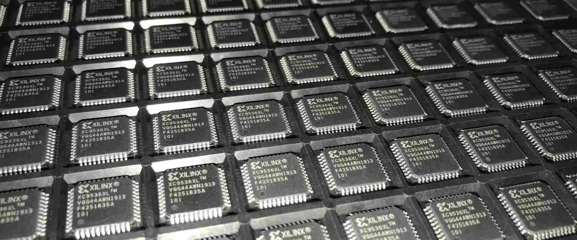
Shenzhen Suntak Technology Ltd is simply a PCB service enterprise. Their products are applicable in industrial control, communication, security electronics, medical instrument, aerospace, power electronics, etc. More than 80 percent of Suntak PCBs get exported to Europe, to America, as well as the other parts of Asia.

What Does Suntak PCB Manufacturing Mean?

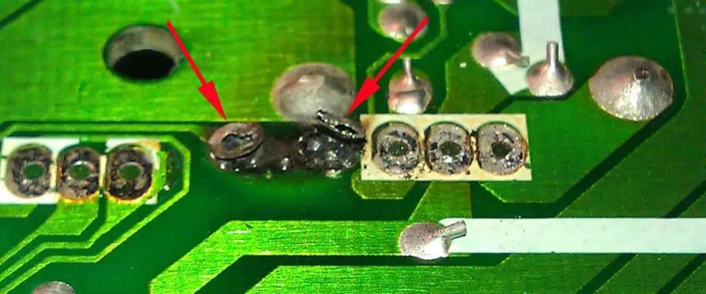
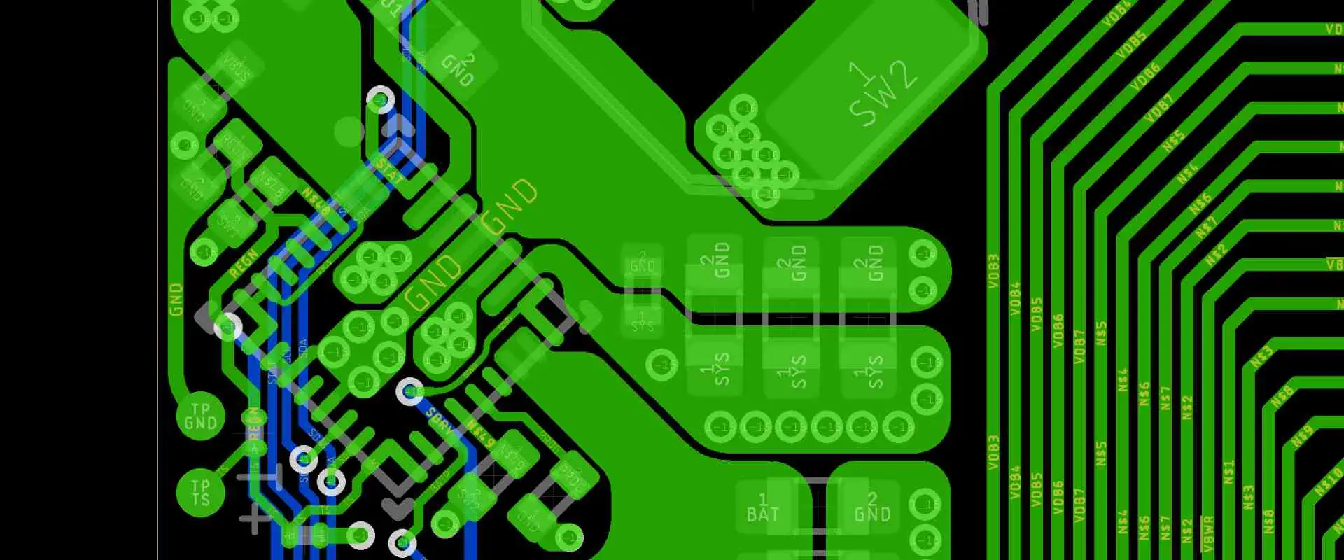
The Process of PCB manufacturing needs a complex procedure. This ensures that the completed product offers great performance. Although circuit boards could be multilayered, double, or single, the processes of fabrication used will only differ after manufacturing the initial layer. As a result of differences in the PCB structure, some may need at least 20 steps during the manufacturing.

The required number of steps for manufacturing PCBs usually correlated with the complexity. If you cut back or skip any step during the procedure, it could impact the circuit boardโ€™s performance negatively. Moreover, when it is completed successfully, the printed circuit boards have to perform each task properly as the main electronic components.

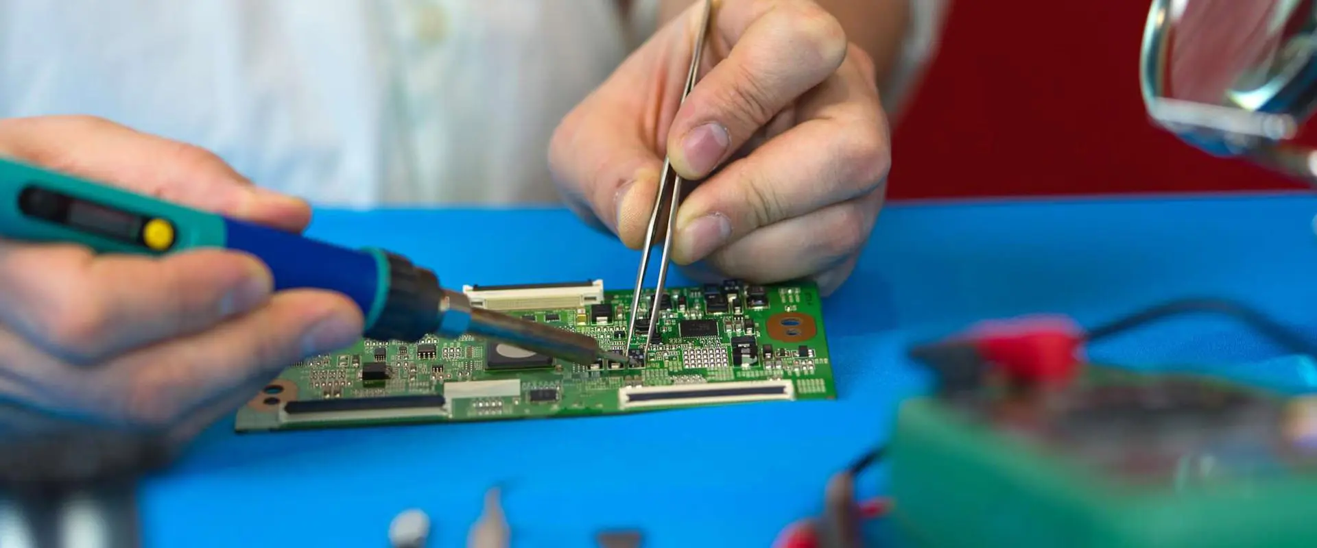
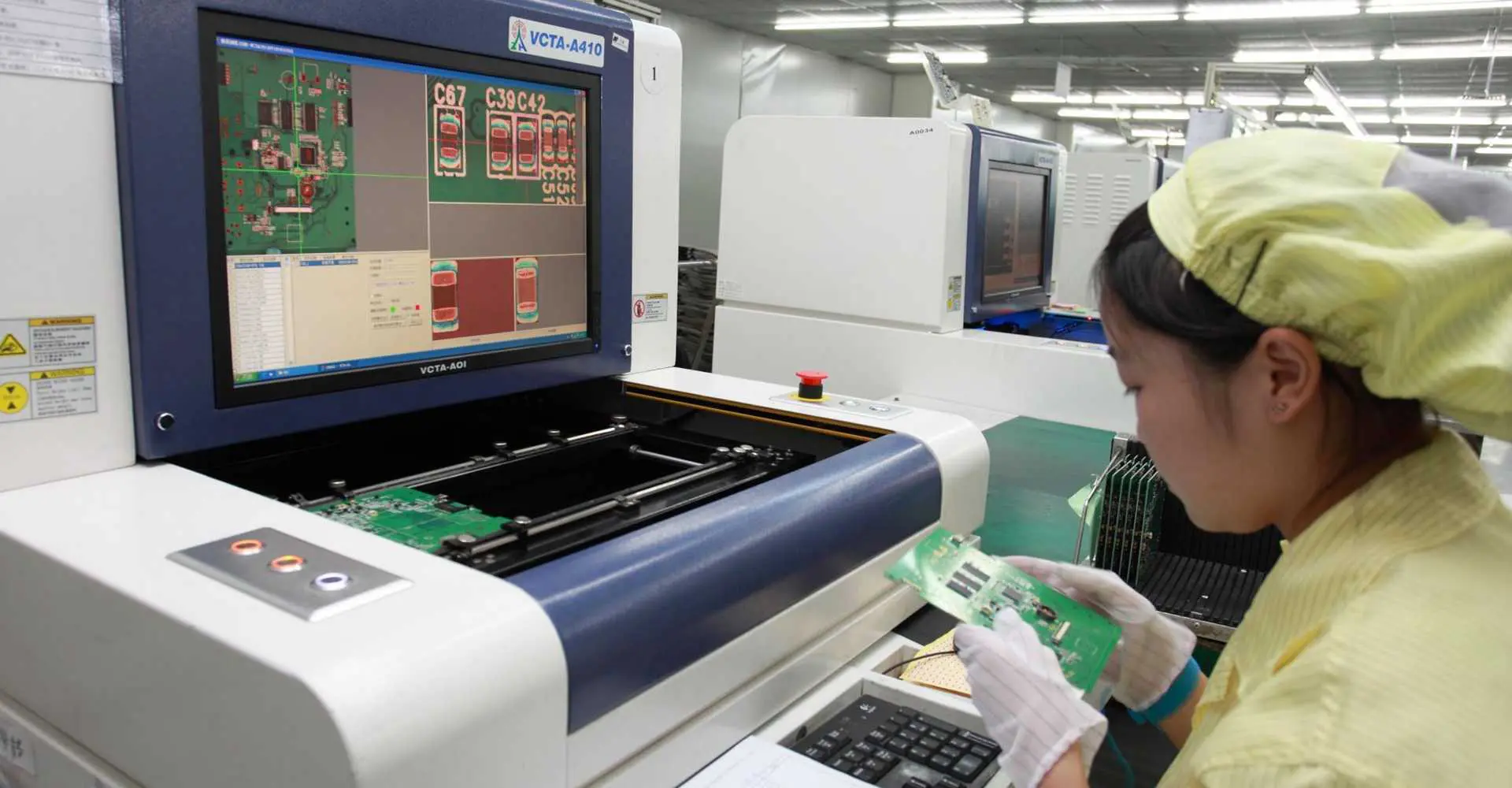
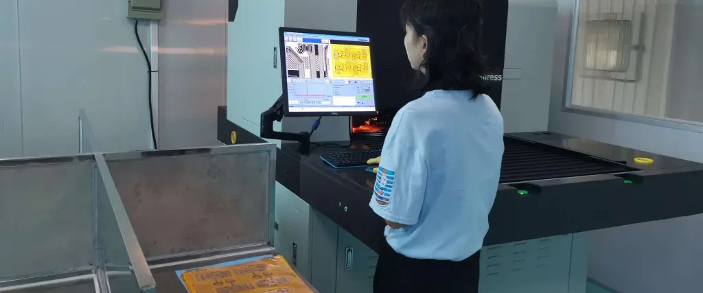
This process begins with the design and the review stages, making use of PCB design CAD tools. It then goes through the board manufacturing. In order to facilitate speed and prevent human errors, many of these steps are machine-driven and computer-guided.

This is important so as to prevent incomplete circuits and short circuits. To ensure quality assurance, these boards are also subjected to some strict testing. This takes place at different points during the fabrication and then finally as completed boards, just before packaging them and shipping them for delivery.

Main Parts of the Suntak PCB

Rogers RO4533

Suntak PCB comes in four major parts.

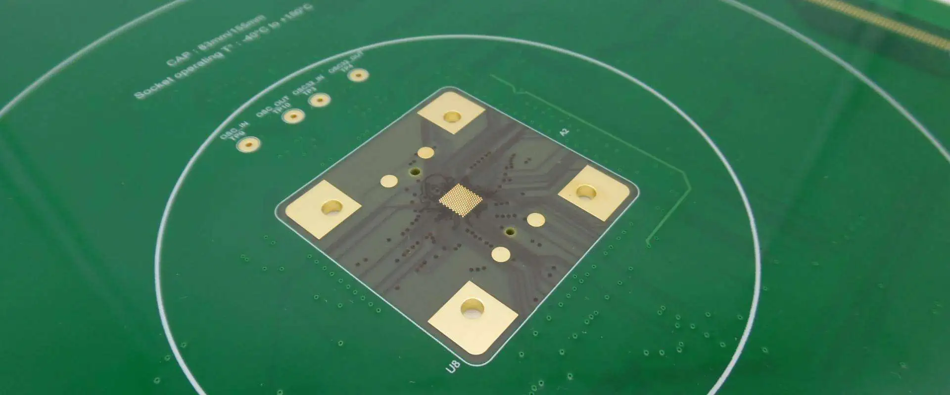
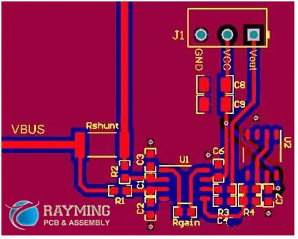
The Substrate: This is the most important, which is usually manufactured from fiberglass. The use of fiberglass is because it offers the PCB its core strength as well as resists breakage. Just consider the substrate as the skeleton of the PCB.

Copper Layer: With respect to the type of board, the layer can be full-on copper coat or copper foil. Regardless of the approach used, the copper point remains the same. It carries the electrical signals to the PCB and from it. This is more like the nervous system carrying signals in-between your brain and muscles.

The Solder Mask: Solder mask is the 3d piece of a printed circuit board, which can be described as a polymer later which offers protection to the copper ensuring that short-circuit donโ€™t happen or have contact with its environment. With this feature, we can say that t5he solder mask is the skin of the PCB.

Silkscreen: The silkscreen is the last part of the printed circuit board. It is usually found on the boardโ€™s component side. It is used for showing the logos, test points, component reference, symbol switch setting, and part numbers. You can also refer to the silkscreen as nomenclature or legend.

What are the Applications of Suntak PCB?

Due to the versatility of Suntak PCBs, they are useful in different electronic devices as well as across many industries. Below are some of the applications of the Suntak PCB.

Consumer electronics

IoT devices, computers, and Smartphones are some of the common devices that require PCBs. Also household electronics like refrigerators and microwaves also rely on printed circuit boards.

As devices are becoming IoT compatible, theyโ€™ll have to use PCBs. PCBs utilized in devices like home assistants and smartphones have to be small, having high connection density. This is because of the complex demands and wide range of the devices.

Automotive Components

The cars of today rely more on the electronic process which older models also did. To ensure this system functions effectively, they utilize different PCBs. The automotive PCBs are useful for proximity and parking sensors, video and audio systems, navigation, fuel regulators, resource management and monitoring, and engine management systems.

Furthermore, modern cars have many sophisticated and interconnected sensors which cannot function unless there is a presence of many advanced high-frequency PCBs. As development continues in the industry, most importantly with advancement in electric vehicles, the demand for printed circuit boards will be higher.

LEDs

This refers to lighting technology across different sectors as a result of their longevity, energy efficiency, and compact size. Automotive displays, electronic signs, smart bulbs, and the laptop screen all make use of LEDs.

Also, PCBs are useful with the LED technology to help in transferring heat from bulbs. If this is not done, it can reduce the lifespan of the LED. The PCBs here are usually aluminum-made, which helps in transferring heat very effectively compared to other metals.

Medical Devices

FULL PCB MANUFACTURING Quote

Printed circuit boards come with different applications in healthcare. They are useful in the medical imaging systems like CAT, CT, and ultrasonic scanners, monitor technology for the vitals like heart rate, blood pressure, internal devices and implants like pacemakers. For these applications, printed circuit boards are HDI models. This is because they have to be extremely small and meet some strict sanitation regulations.

Aerospace

Flexible printed circuit boards are very important for the aerospace technology. The aerospace vessels usually experience huge turbulence during flights and the rigid PCBs can get damaged easily. However, the flexible PCBs are designed light and are resistant to possible vibration damage.

These precise and high-functioning PCBs are useful for different aerospace applications like communications equipment, power supplies, and monitoring equipment.

Industrial Equipment

These equipment like high-powered presses and drills functions making use of PCB electronics, as with equipment used in measuring and controlling variables like temperature and pressure during the process of manufacturing.

Also, PCB come in different types and are necessary for different industrial equipment. This depends on the specific application. Many PCBs must be durable so as to withstand harsh conditions like intense machinery vibration, exposure to any harsh chemicals, electrical circuits of high voltage, and extreme temperatures.

Conclusion

PCB or Printed circuit boards offer electrical and mechanical support for the electrical devices. Also, they are useful for connecting the electronic components making use of signal traces and conductive pathways from the copper sheets that are laminated on the non-conductive substrate. Any questions, please reach out to us.

What Are XC6SLX9-2TQG144I FPGA And Its Advantages?

wholesale Xilinx FPGA

Nowadays, you cannot expect any device without FPGA. FPGAs are an integral part of every electronic device nowadays. You can find several FPGAs in the market with different specifications. The manufacturer of the XC6SLX9-2TQG144I is Xilinx. This FPGA belongs to the Spartan-6 family of FPGAs developed by Xilinx. The Spartan-6 family of FPGAs is known for its low power consumption and high performance. In addition to its flexibility, making it suitable for a wide range of applications in industries such as automotive, telecommunications, industrial, and consumer electronics. Let’s have a close look at its specifications.

Specifications of XC6SLX9-2TQG144I

The XC6SLX9-2TQG144I has the following specifications that make it stand out among all FPGAs.

1. Logic Cells

Logic cells are the basic building blocks. You can’t expect any FPGA without these logic cells. Moreover, these logic cells are essential for all basic functions. The XC6SLX9-2TQG144I contains 9,152 logic cells.

2. DSP Slices

Digital signal processing is possible due to these slices. The XC6SLX9-2TQG144I contains 576 simple slices. These Slices are groups of logic cells that are interconnected. Asa result, you can perform more complex functions. They are particularly useful for different applications. Digital signal processing and image processing are examples. This FPGA has 48A1 DSP slices. These are enough to perform the necessary functions. You can program the XC7A15T-1CSG324C using these DSP Slices.

3. Block RAM

Block RAM, AKA BRAM, is great for data storage. Block RAM typically consists of multiple RAM blocks. That’s why they are configured and connected to the FPGA fabric to meet specific needs. The XC6SLX9-2TQG144I contains 180 block RAMs. Block RAMs are helpful for storing data in the FPGA.

4. Clock Management Tiles

The XC6SLX9-2TQG144I contains 4 clock management tiles. Clock management tiles help to generate and distribute clock signals within the FPGA. Every FPGA has a different clock management system.

5. Maximum Frequency

The XC6SLX9-2TQG144I can operate at a maximum frequency of 250 MHz. It is the ideal frequency.

Input and output Pins

The XC6SLX9-2TQG144I contains 92 Input and output pins. Input and out pins are used to connect the FPGA to the external world.

Power Specifications of Operating Voltage

Xilinx Spartan
Xilinx Spartan
  • The FPGA operates at a voltage range of 1.14V to 1.26V. It is quite a normal voltage.
  • The maximum power consumption of the device is 1.0 watts when operating at its maximum frequency.
  • The FPGA supports advanced power management features. For example, programmable voltage scaling and dynamic power management support power management. These systems also help with power-optimized configurations.

It is important to note that these power specifications are based on typical operating conditions and may vary depending on the specific application and usage scenario.

Alphanumeric Breakdown Of FPGA

If you don’t know much about the FPGAs, then you may consider it just number and alphabet. Alpha Numeric Break Down of XC6SLX9-2TQG144I provides basic information regarding FPGA.

  • XC6 indicates that the FPGA belongs to the Spartan-6 family.
  • S indicates that the FPGA is a high-speed grade.
  • L indicates that the FPGA has a low-power mode.
  • X9 indicates that the FPGA has 9,152 logic cells.
  • 2T indicates that the FPGA has 2 DCM tiles.
  • QG144 indicates that the FPGA comes in a TQG144 package.
  • I that the FPGA is industrial grade.

 Advantages of XC6SLX9-2TQG144I

 This FPGA provides the following advantages.

ยท High-Performance Computing and Processing

One of the most impressive features of XC6SLX9-2TQG144I is its high-performance computing capabilities. This FPGA offers up to 250 MHz high speed. That’s why this FPGA is capable of handling complex computing tasks. It is an idea for applications that require real-time data processing and analysis.

The XC6SLX9-2TQG144I features a range of versatile input and output interfaces, including high-speed serial interfaces. For example, SATA and PCI Express, Ethernet ports, and USB interface. It can easily connect the device to a variety of different systems.  

That’s why it is ideal for use in a wide range of applications and fields. As a result, all hi-tech devices have this FPGA as the main component.

ยท Low-Power Design for Efficient Energy Management

Power management is necessary for the ideal working of a device or system. Despite its impressive computing capabilities, the XC6SLX9-2TQG144I is designed to be energy-efficient. Its low-power design helps to minimize power consumption and extend battery life. This makes it ideal for use in hi-tech portable devices; similarly, it is ideal for battery-powered devices. It is also ideal for applications where power management is a critical issue. Above all, it is an ideal FPGA.

ยท Built In Memory for Data Storage

FULL PCB MANUFACTURING Quote

The XC6SLX9-2TQG144I also features built-in memory. It has up to 180 Mb of block RAM. Moreover, up to thirty-six Mb of distributed RAM is icing on the cake. This makes it easy to store and access data on the device itself. It also reduces the need for external memory. As a result, it simplifies the design of complex systems.

ยท Package Type

 Package type is very important when it comes to FPGAs. The XC6SLX9-2TQG144I comes in a TQG144 package. The TQG144 package is a type of packaging for integrated circuits and FPGAs. In addition, the package is a plastic quad flat pack (PQFP). It contains a total of 144 pins arranged in a grid pattern with a 0.5mm pin pitch. As a result, product remains intact. That’s why The TQG144 package is used for several FPGA families. For example, Xilinx Spartan-6 and Altera MAX II are the families that use this TQG144 package.

Final Words

The XC6SLX9-2TQG144I is a cost-optimized FPGA. As a result, it provides high performance and low power consumption. Its specification and alphanumeric breakdown have been discussed in detail in this article. Lastly, with its large capacity, the XC6SLX9-2TQG144I FPGA can handle complex designs and processes. As a result, it is a versatile solution for a wide range of applications. Moreover, from industrial control systems to telecommunications equipment, you have this FPGA in systems. In addition, the technical advantages of the XC6SLX9-2TQG144I FPGA make it a powerful and flexible solution. That’s why if you are looking for cutting-edge technology-based FPGA, then go for it. It will not disappoint you at all. 

What Is HMC349MS8GETR? Detailed Overview of Its Specifications.

pic programming Vs. microcontroller programming

An FPGA is made up of a large number of configurable logic blocks and interconnected programmable routing channels. These blocks and channels are easy to reconfigure. You can use different software tools for this purpose. It allows users to implement complex digital circuits on a single chip. HMC349MS8GETR is a bit different from typical FPGA or typically integrated circuits. Let’s dig deeper to know more about this HMC349MS8GETR.

 What Is HMC349MS8GETR?

The HMC349MS8GETR is a monolithic Gas MMIC SPDT switch.  Moreover it is suitable for high-performance applications from DC to thirteen GHz. It is ideal due to its practical features, such as low insertion loss, high isolation, and high linearity. That’s why it is ideal for use in RF and microwave systems. Suppose you list its applications.  As a result you will have a long list.

Features And Specifications

The HMC349MS8GETR is a versatile device. That’s why it is used in different devices. Some of the key specifications are following

  • It has an optimal Operating frequency range from DC to 13 GHz.
  • Insertion loss for this device is 0.3 dB at 1 GHz, 0.5 dB at 10 GHz. However you can overcome this loss. As result you have better performance of FPGA.
  • Isolation for HMC349MS8GETR: 48 dB at 1 GHz, 30 dB at 10 GHz.
  • Input IP3 is 60 dBm at 1 GHz, 50 dBm at 10 GHz.
  • Supply voltage range from 3 V to 8 V for this device.
  • Power consumption is typically 20 mW. As a result it is ideal for wireless applications.

These specifications make the HMC349MS8GETR highly capable of doing versatile functions. It can easily switch between RF and microwave systems. It offers low insertion loss, high isolation, and high linearity.ย ย 

Clock And Reset Specifications

FULL PCB MANUFACTURING Quote

 Accurate timing signals to operate correctly and the HMC349MS8GETR is no exception. Here is some of the clock and reset specifications for this device:

  • Input clock levels for HMC349MS8GETR are LVDS, LVPECL, CML, SSTL, HCSL, etc
  • The input frequency range for the clock signal is 5 to 10 GHz for HMC349MS8GETR
  • The input power range for the clock signal is -5 to 10 dBm for HMC349MS8GETR
  • The conversion loss for the HMC349MS8GETR is typically 7 dB. It can vary according to the voltage
  • The input impedance for the clock signal is 50 ohms, and phase noise for the HMC349MS8GETR is typically -135 dBc/Hz at 100 kHz offset

Reset Specifications for HMC349MS8GETR

The reset specifications for the HMC349MS8GETR are as follows. These specifications are simple, and designers can easily understand them.

Input Pulse Width

  • The input pulse width for the reset signal is 100 ns with a power range of 5 to 10 dBm.
  • The output pulse width for the reset signal is 1 ยตs, with rise and fall times for the reset signal being 10 ns.

Gain For HMC349MS8GETR

The HMC349MS8GETR has a gain of up to 19 dB. You can adjust this gain by using external resistors. In addition, the gain flatness of the is typically ยฑ1.5 dB. But still, there is a chance to improve it. Similarly, it differs from FPGA to FPGA.

Noise Figure for HMC349MS8GETR

 Noise management is important to work with HMC349MS8GETR. The HMC349MS8GETR has a typical noise figure of 2.2 dB. You can control or reduce the noise figure by increasing the gain of the amplifier.

Input And Output Impedance for HMC349MS8GETR

 You can neglect impedance when working with HMC349MS8GETR. The HMC349MS8GETR has a typical input impedance of fifty ohms. As a result, it is important to control the input and output impedance. Moreover, you can adjust impedance by using external matching networks. There are some other ways to control this impedance.

Biasing The HMC349MS8GETR

 Braising is one of the basic requirements of the HMC349MS8GETR. That’s why The HMC349MS8GETR requires a supply voltage of three volts. Similarly, it consumes a maximum of 85 mA of current, but it depends upon the requirement.  

Ideal Operating Temperature

ย As you know, the ideal temperature varies from device to device. Ideal or optimum temperature means at which the device can work efficiently. The HMC349MS8GETR can operate at temperatures ranging from -40ยฐC to 85ยฐC. It is the optimal temperature for the best functioning. If the temperature is less than -40ยฐC, then it will affect its functioning.

Applications Of HMC349MS8GETR

 You can use The HMC349MS8GETR in a variety of high-frequency applications.

ยท Wireless Infrastructure

Designers always look for a versatile IC when they design any wireless infrastructure.

The HMC349MS8GETR is suitable for use in wireless infrastructure applications, including base stations and repeaters.

ยท Test And Measurement Applications

The HMC349MS8GETR is also suitable for use in test and measurement equipment. For example, spectrum analyzers and signal generators have wide use of this HMC349MS8GETR.

ยท Mobile Radio And 4G Infrastructure

This HMC349MS8GETR is a logic device and is great to incorporate into 4G infrastructures. That’s why its demand is increasing day by day. It is easy to integrate and bring fruitful results; as a result 4G infrastructure provides better results. Similarly mobile radio also has a special place for it. 

Frequently Asked Questions

ยท What Is the Frequency Range of the HMC349MS8 ETR?

The HMC349MS8GETR has a frequency range of 0.1 GHz to 40 GHz. The frequency range varies from device to device. How do designers integrate this HMC349MS8GETR in their systems or in different applications? That’s why it is important to keep different technical aspects while using HMC349MS8GETR.

ยท What Is the Packaging of HMC349MS8GETR?

 HMC349MS8GETR comes in an 8-lead MSOP package. As a result this packaging is a Lead-free, RoHS-compliant package. That’s why it is easy to integrate into systems.  Furthermore, it operates from a single positive voltage. It also consumes low power, and that’s why it is suitable for battery-powered applications.

Final Thoughts

HMC349MS8GETR is modern FPGA. By understanding the input/output specifications of the HMC349MS8GETR, you can easily utilize it in different applications.  Thatโ€™s why Designers can make informed decisions and avoid loss. As a result, they can creatively use it in their designs and applications. That’s why we consider it a versatile device. Now it is up to the designers and engineers how they use it so perfectly.

EP4CE40F23I7N, Its Specifications, And Configuration

EP4CE40F23I7N

If you are a designer and currently working on a project that requires an FPGA, then what would you choose? You need FPGA with unwavering potency and dependability. The EP4CE40F23I7N presents itself as a top-notch option. This FPGA, hailing from Altera, boasts exceptional performance and remarkable adaptability. That’s why it is suitable for a wide array of uses. In the following content, we shall elucidate the technical specifications of the EP4CE40F23I7N and the configuration process.

Technical Specifications

  • This FPGA EP4CE40F23I7N belongs to the Cyclone IV E family.
  • It comes in the FBGA Fine-Pitch Ball Grid Array package
  • This FPGA EP4CE40F23I7N contains l39, 600 logic elements.
  • It contains 1,386 Kbits number memory elements
  • EP4CE40F23I7N contains 4 Phase-Locked Loops
  • It contains 484f user Input and output pins
  • 2V is the maximum operating voltage for it at speed grade 7
  • Maximum operating frequency for FPGA EP4CE40F23I7N 462MHz

 Let’s dig deeper into its specifications.

This FPGA belongs to the Cyclone IV E family. This family is famous for providing a low-cost, low-power solution for various applications. The EP4CE40F23I7N is a mid-range FPGA that offers a good balance between performance and cost-effectiveness. It has a large number of logic elements, which makes it suitable for implementing complex digital circuits. It also has a significant amount of memory elements.

 Supportive Logic Elements

The EP4CE40F23I7N has a total of 39,600 logic elements. An LE is the smallest building and basic building block of an FPGA. As a result, it is easy to implement logic functions. You can see that these logic blocks are the bricks of the FPGA building.

Memory Storage

The EP4CE40F23I7N 1,122 embedded memory blocks. These are used to store data in the FPGA. That’s why you can use it for various purposes, such as buffering. Moreover, it is supportive of storing configuration data.

 Best Digital Signal Processing

Better signal processing is important when it comes to FPGA. Thatโ€™s why This FPGA has Two hundred sixty-six embedded 18 x 18 multipliers. As a result, these are helpful for multiplying two numbers together. Moreover, these are useful in a variety of applications, such as digital signal processing.

Stable Clock Signals

4-phase locked loops help to generate stable clock signals, which are essential for the proper operation of the FPGA. That’s why its signal processing is at its best. It also has many other supportive features to support clock signaling.

Input And Output Pins

 It has Up to 622 user input and output pins. As a result, connectivity and integration are so easy.

Thatโ€™s why it can adjust multiple interfaces. As a result, this FPGA can go to other devices and can be configured as inputs or outputs. Support for a range of interfaces, including DDR3 PCIe and Gigabit Ethernet. These are commonly used communication protocols and interfaces. As a result, this FPGA can communicate with other devices and systems.

Configuration Scheme for the EP4CE40F23I7N

FULL PCB MANUFACTURING Quote

 EP4CE40F23I7N FPGA is easy to reprogram. It is manufactured by Intel (previously known as Altera). The configuration scheme for this FPGA is comprised of loading configuration data into the configuration memory.

  • For this particular FPGA, the configuration scheme involves utilizing a 1.8V configuration device. For example, an EPCS128 or EPCS64 serial configuration device can retain the configuration data. The connection between the FPGA and the configuration device is easy to establish through the Joint Test Action Group interface. As a result, it is easy to transfer configuration data from the device to the FPGA.
  • The programming object file stores the configuration data. Quartus Prime software is helpful in POF file generation. The POF file has the configuration device with the use of a programming tool, such as the Quartus Programmer or the USB-Blaster.
  • When the configuration process is underway, the configuration device moves the configuration data into the configuration memory of the FPGA. Once the configuration is complete, the FPGA is ready to execute the design of the user.
  • It’s worth noting that the specific design requirements and programming tools can alter the configuration scheme. That’s why it is necessary to consult the device datasheet and the documentation for the programming tools. As a result, you can acquire specific details about the configuration.
  • Finally, the FPGA is configured using an SRAM-based configuration scheme. Moreover, it allows for easy reprogramming of the device. That’s why it is suitable for applications where the functionality of the circuit needs frequent change. Overall, it is a simple but tricky process.

ย 

Break Down of Alphanumeric Coding of FPGA EP4CE40F23I7N,

 This code is actually a part number or model number for an electronic component. Here’s what each part of the code represents, but if you have a bit of knowledge of FPGA coding, then you can easily understand the coding.

  • EP shows Altera Cyclone IV E, which is the family of FPGAs that this particular FPGA belongs to.
  • 4CE refers to the specific Cyclone IV E device. The 4 indicates that it is a fourth-generation device, and “CE” is part of the code name for the Cyclone IV E family.
  • 40 indicates the number of thousands of logic elements in the device. In this case, the chip has 40,000 LEs.
  • I7 is the temperature grade of the device. I indicate the ideal temperature is between -40ยฐC to 100ยฐC.
  • 7 indicates the year of the product introduction.
  • N indicates that the device does not have any additional special features.
  • F23 represents the package type and speed grade of the device. In this case, F2 means that the chip is in a 484-pin fine-line BGA (Ball Grid Array) package. That’s why it has a maximum speed of 230 MHz.

To Conclude

I hope now to have a better understanding of this FPGA. What are its specifications, and what numbers are indicated? I tried my best to explain each and everything in detail. Above all, this is a cost-efficient FPGA, and it can easily integrate into different applications and systems. That’s why if you are looking for an ideal FPGA for your next project, then you must go for EP4CE40F23I7N FPGA.

Why you need to Consider the PTFE Dielectric Constant in your Application

PTFE Dielectric Constant

Polytetrafluoroethylene, which is also known as PTFE, is one of the commonly used materials for producing printed circuit boards. This material has its unique electrical and dielectric properties which makes it an ideal choice for PCBs. It has got stable electrical properties which are stable in terms of temperature and frequency.

PTFE has mechanical, thermal, dielectric, and electric properties. However, we are majorly looking at the dielectric properties of PTFE, particularly the dielectric constant.

What is PTFE?

Polytetrafluoroethylene (PTFE) is a plastic material that comprises carbon atoms with fluorine atoms attached to each carbon. This plastic material is a high-performance fluoropolymer used in the production of printed circuit boards. As the second most popular PCB  material, PTFE offers stable and consistent dielectric properties at a higher CTE.

Due to the properties if PTFE , it is widely used in higher-frequency and higher-speed applications. The microwave technology is one of the application areas of PTFE. PTFE is a form of polymerized tetrafluoroethylene.  The combination of fluorspar, chloroform, and hydrochloric acid is what produces Polymerized tetrafluoroethylene. Tetrafluoroethylene (TFE) goes through pressure which is then stored in a liquid state. This usually occurs before the production of PTFE.

Asides from being used in the production of printed circuit boards, PTFE is widely used in industries like chemical processing, construction, oil & gas, electronic, and more. This material is resistant to light, heat, and chemical. In kitchen cookware, PTFE serves as a non-stick coating.

Without any doubt, fluoropolymer belongs to a class of plastics. It offers various properties. The emergence of fluoropolymers was revolutionized due to the discovery of Polytetrafluoroethylene. These days, the applications of PTFE range from non-stick frying pan surfaces  to exotic medical and hospital uses such as test equipment, implants, and surgical instruments. Also, you will find its use in firefighting equipment and a lot more.

Out of many plastic materials, PTFE features the best dielectric property. This material is widely used in several applications due to its dielectric and electrical properties. Teflon dielectric constant also means Teflon relative permittivity.

What is PTFE Dielectric Constant?

PTFE teflon pcb

The dielectric constant of PTFE is 2.02. PTFE has a low dielectric constant that remains stable in response to changes in frequency and temperature. The dielectric constant is an important dielectric property which measures the capability of a material to store electrical energy when it is in an electric field.

It could also be defined as the ratio of a materialโ€™s permittivity to a free spaceโ€™s permittivity. Due to PTFE low dielectric constant, this material is much better than standard FR4. Also, the dielectric constant of PTFE makes it suitable for overcoming the limitation of FR-4.

Polytetrafluoroethylene is used as a base material for printed circuit board. Also, the PTFE dielectric constant makes it suitable for high-frequency applications. PTFE is known to be a poor conductor of electricity since it has a low dielectric constant.

Since PTFE is a non-polymer with one polarization mechanism, it has a low dielectric constant. Teflon dielectric constant is a indicator that this material is a good insulator. Therefore, it is ideal for high-frequency microwave substrates.

Also, PTFE can reduce the loss of electric power when used in printed circuit boards.

Applications of PTFE

Due to the excellent dielectric properties of PTFE, this plastic material has found its use in a wide range of applications. PTFE is widely used in various applications. This material is suitable for making liners or tubes where corrosive chemicals are stored. However, you can as well use this material to coat screws or bearing in order to extend the life span of these tools.

You will also find them in medical applications such as the production of life-saving equipment like syringes and catheters.

Medical devices

Polytetrafluoroethylene is a material used in the production of medical devices. Due to its inertness and biological adaptability, PTFE doesnโ€™t have any physiological side effects. Also, expanded PTFE isnโ€™t rejected in the body. Therefore, this material is ideal for use in different rehabilitation solutions such as patches for soft tissue regeneration, plastic surgery, and artificial blood vessels.

Electronic devices

Due to PTFE dielectric constant and low loss, this plastic material can be transformed into enameled wire for control devices, and micro motors. The PTFE film is a great material for producing radio insulation limes, transformers, radio insulation liner, and more.

Automotive

PTFE has also gained popularity in the automotive industry due to its thermal stability and low dielectric constant. This material maintains thermal stability when used for engine parts and vehicle exteriors. Also, PTFE provides leak-proof technologies with more reliability at high temperatures and speeds. Also, PTFE found its use in the automotive industry as a result of its resistance to corrosion.

Polytetrafluoroethylene can resist flames and as such, it is more useful in equipment used under very extreme conditions. This material is water resistant and as such it is great for the glass windshields and wiper blades in vehicles.

Benefits of PTFE Coating

FULL PCB MANUFACTURING Quote

Due to the non-stick nature of PTFE coatings, it is mostly used in applications like commercial bakeware. This bakeware is usually easy to clean.  PTFE is capable of repelling oil and water and as such a PTFE-coated screw can resist corrosion. This screw can be lubricated to work perfectly into any surface you intend to fasten it to.

PTFE surfaces are oleophobic and donโ€™t get readily wet. Due to its self-cleaning property, it is widely used in the semiconductor industry. Its self-cleaning and hydrophobic property is crucial for running off all chemical media. When PTFE coatings offer non-stick or release properties when applied to a component.

Also, PTFE coating helps in preventing cold and hot products from sticking to the substrate. Therefore, this form of coating is ideal for use in bakery and confectionery industries. You will also find out that PTFE coatings are suitable for non-stick in the aerospace, moulding, pharmaceutical, and packaging industries.

PTFE has non-wetting capability which helps in minimizing cleaning of equipment. Also, this material is environmentally safe. It is certified by the FDA and considered safe for humans. This material has no toxicity and as such it is considered a green material for printed circuit board manufacturing. Teflon relative permittivity makes it a great option for various applications

Properties of PTFE

PTFE features excellent properties which make them a unique plastic material for some applications.

Excellent electrical properties

PTFE features excellent dielectric strength, high surface resistivity, and a low dissipation factor. Therefore, this materials offers protection when used in several electrical applications. Also, PTFE can become conductive and serve as an antistatic coating. This material is an efficient electrical insulator and as such it is usually used in electrical cables and PCBs.

Temperature resistance

One of the main properties of PTFE is temperature resistance. PTFE coatings can be used in devices or items that are exposed to extreme temperatures. The temperature of these coatings can be stable at elevated temperature of +260 degrees Celsius. Also, PTFE can serve as extrusion dies of elastomers where they can be clogging or degradation of molten materials due to other treatments. Also, PTFE coatings can remain stable even at -270 degrees Celsius.

Chemical and corrosion resistance

PTFE can withstand corrosion and chemical. It can resist most chemicals. When PTFE is combined with fluoropolymers, it improves the life of components. Also, when PTFE is applied to a surface, the resistance of a component to corrosion will increase. You can as well enhance PTFE by using primers and other pre-treatments like phosphating.

Low dielectric constant

Teflon dielectric constant is 2.02. PTFE has a low dielectric constant that remains stable in response to changes in frequency and temperature.

Abrasion resistance and low friction

PTFE can minimize friction and as such can help in achieving low friction coefficients ranging from 0.04 to 0.15. In cases where grease and oil respond to high temperatures, PTFE is stable. Therefore, PTFE is suitable for moving mechanisms, shafts, fasteners, and stud bolts. You can reinforce PTFE coating by adding fillers and combine a metal sprayed base layer. This helps in improving the wear life and abrasion resistance of PTFE. Also, adding fillers to PTFE can serve as a reinforcement.

Anti-galling

This is a unique property of PTFE coatings. PTFE coatings offer great bearing properties and as such prevent galling. These coatings are beneficial to rotating parts and mating surfaces. Also, they can offer low maintenance downtime.

Disadvantages of PTFE

PTFE has its disadvantages despite the benefits it offers. However, the disadvantages of PTFE depend on the application. As a great material, PTFE is ideal for use in different applications. The disadvantages of this material can rule out the use of PTFE in some applications.

  • PTFE canโ€™t be welded
  • This material has the ability to change shape when it is under pressure
  • Mass production of PTFE isnโ€™t easy
  • PTFE isnโ€™t a low-cost polymer

Conclusion

PTFE is a common material used in PCB production. It offers great electrical and dielectric properties which make it stand out among other plastic materials. Due to PTFE excellent properties, this material is mostly used in applications which range from food coverings to cooking equipment, temperature sensor, and conveyor belt rollers. T

What Is PCB Trace Resistance Calculator? A Comprehensive Guide

pcb trace resistance calculator

No PCB design can be perfect without paying attention to the trace width. If you want to come up with a flawless PCB design, you need to maintain the trace width on all counts.

 In this pursuit, you can seek help from some factors that make determining accurate trace width easier. It is important to understand what trace width is and its functionality before jumping on its determining factors. 

In this post, we are going to have an insightful look at trace width for you! So letโ€™s get started!

YouTube video

What is PCB Trace Width?

The purpose of trace width is to combine signals from one part to the other. It is also useful for stabilizing these signals to avoid any problems. Now, these parts can be anything. 

From pins to junctions and wires, smooth signaling happens only if you set an accurate trace width. Due to this reason, trace width is an important factor to consider when designing PCBs. 

It will also help in protecting the PCBs in case the temperature exceeds the limit. A PCB trace is like a wire that has great durability to handle large amounts of current and electrical loads. 

The heat dissipates when a large amount of current passes through a system. For this, trace width comes in handy. If not handled carefully, insufficient trace width can lead to irreversible damage to the PCBs. 

Traces do not need any kind of resistance to function properly. They can join the PCB parts without any external assistance. To ensure everything is in place, you must determine the current, resistance, and amount of temperature when designing a specific PCB.ย 

What is a PCB trace resistance calculator?

A trace wish calculator can prove to be useful in this aspect. It functions to measure the PCBโ€™s width precisely. It is a complex device that uses programming languages to make sure the reading is accurate. 

Trace width is important for developing flawless PCBs, and for an accurate trace width, you need to rely on a trace width calculating device.

 One major benefit of using trace width is that it regulates the temperature of PCBs when large currents pass through the critical components inside. 

Letโ€™s check out other upsides of using a trace width calculator:

  • It is useful to get multiple readings like voltage changes, temperature changes, power loss, and amount of current/resistance.
  • Such a calculator can also read the amount in amperes, making it easier when you are designing PCBs.

When you are taking reading in amperes, you must know that it can vary as per the length of the current path. In case you don’t determine such parameters before using the calculator, you cannot get an accurate reading in amperes at all. 

The calculator works on your pre-determined factors. The trace width will then protect the PCBs and will regulate the current flow without letting it damage the board itself. 

Internal layers of the boards have a large amount of trace width than those present outside. The trace width directly relates to the heat produced, and internal layers generate more heat since their trace width is higher than the external ones. 

To ensure 100% security of the PCBs, it is important to pay great attention to trace width of internal layers. It is because they bear excessive load during the working of PCBs. 

Applications of PCB trace resistance calculator

The margin of error when you use a trace width calculator, becomes less. No PCB can guarantee perfect performance if you don’t calculate its trace width in the first place. There are some key applications of this calculator that you need to know when it comes to designing excellent PCBs.

  • Such a calculating device can measure small to large trace widths easily without interfering with the current path.
  • You can also determine the factors to take precise readings with the least hustle when using this calculator.
  • You can rely on this calculator to take readings for internal and external layers of PCBs.
  • The trace width measured by a calculator is helpful when it comes to power tracing, and power signal uses cases.

Types of PCB trace resistance calculator in the Electronics Industryย 

FULL PCB MANUFACTURING Quote

You must be wondering if there is only a single terrace width calculator available. That’s not true. There are many types of calculators available that you need to choose from as per your requirements. 

These are state-of-the-art calculators that meet all the industry standards. However, we are going to discuss two typical calculators in this section.

IPC 2221 PCB trace resistance calculator

The IPC 2221 functions on a mathematical equation and uses a graph to record the readings. The calculator uses the I=kฮ”TbAc equation to get you proper readings. 

The amount of K for the visible and internal traces differs when you follow this equation. The equation also shows the temperature changes as per the area for which the calculator is recording the reading. 

When using this calculator, you need to add perfect values for the equation. The current must be up to 35 amperes. Keep the temperature changes between 10oC and 100oC. In case you don’t pay heed to these values, the results won’t be accurate at all. 

IPC 2152 PCB trace resistance calculator

Now this is another type of trace width calculator. The calculator works on a similar equation as described before. Experts believe that this variant is more precise than the former one for recording trace widths for PCBs. 

There are different factors to keep in mind while using this device. 

Following are the factors that you should determine to get the best results from this calculator:

  • Distance between passing tracks and copper planes
  • Thermal conductivity of PCBs
  • Amount of current passing through the components
  • Thickness of the passing tracks

Guidelines for Calculating PCB trace resistance 

Every system or device has a set of guidelines that you must follow to procure the desired results. Similarly, when you are using a trace width calculator, there are some rules that will make this process much easier for you every time. Thus, you will be able to save a lot of time as well. 

  • The trace width depends on the type of PCB design and the amount of current going through the tracks.
  • Keep the traceroute up to 10 mm/A at least.
  • Use the copper planes of 1.0 oz/ft2 if you are following the traceroute as mentioned above. 
  • Make sure to determine the thickness, temperature, and unit in which you are going to record the trace width. 
  • These values are important to receive accurate input ranges.
  • Now this input data will get you an output figure which is basically the trace width.

Bear in mind that the input figures have to be accurate, or else the calculator will mess up the final data later. It is better to use a magnifying glass to double-check the input data if your PCB is small when it comes to getting precise trace width calculations. 

Things to consider while Choosing PCB trace resistance calculator

It is clear that trace widths of PCBs can create a negative impact on their performance in case of errors. There are some factors that help in excluding the slightest chance of faults and ensure accurate results. 

1. Signal integrity 

The digital routing for almost all the PCBs has a set of pre-determined data for their trace widths. However, this data can vary as per the size of the boards. Consider impedance nets. 

You need to record their trace width as per the layer stack-up of PCBs. On the other hand, if you are considering analog routing, its trace widths are always different. Try to lower the trace width in congested spaces to get the best reading later. 

2. PCB fabrication

Sometimes you need to fabricate the PCB. It is much easier when you give enough room to its trace width. It also leads to effortless etching when there is more space, and the trace wires are separate.

 So always keep the traces broad when you want to fabricate PCBs without any hustle. If a trace is long, it will provide more tolerance than a short trace. 

3. Power & grounding routing

Traces have major applications in power and ground routing. In this case, traces have to be long so that these wires can allow large currents to pass through. Thin traces are more sensitive, and heat can easily damage them, leading to future problems. 

Also, traces for the internal layers need to be large so that they can help in more dissipation of heat. When used in power supply, trace wires must be broad enough to allow large currents to pass through without any interference. 

The Final Say

A PCB trace calculator is a huge asset when it comes to designing PCBs. It gives accurate readings on temperature shifts, voltage changes, power changes, and much more. 

You now have a vivid idea about why trace widths are important for PCB designing and how you can maintain them through a calculating device for PCBs and other applications. 

What is Lifted Pad and Issues on Printed Circuit Boards?

lifted pad

Circuit board pads serve the purpose of creating a connection between the pins of components and the plates of copper. However, if PCB possesses lifted pads, then pins cannot make a proper and clean connection which damages the electrical components of the PCB. 

Pad lifting is mostly seen in the assembly of single-layered PCB. Moreover, pads will not occur mostly in through-hole PCBs. Sometimes, it may occur rarely. Pad lifting seems considerable, mostly in situations where you face high pressure and high temperature in the assembly process.ย 

YouTube video

Causes Of Lifted Pad On PCB

After the process of wave soldering, mostly in single-layered PCB, the surface of the board heats up, which lowers copper adhesion. Therefore, any time of force or pressure over the electrical components leads to lifting. Hence, consider two different aspects. The physical and thermal aspects. Any additional heat during the assembly of the wave soldering process and additional force to handle the circuit makes components loose and creates pad lifting.

Tips To Avoid Lifted Pad On PCB

How to repair Lifted Pad on PCB

However, a question arise whether there is any solution that may help in avoiding pad lifting in circuit boards. Thus, one can prevent the board from pad lifting with a thermal factor. Try to utilize adhesive or epoxy that has high heat resistance. But this seems unavoidable and high capacity and long-lasting heat may minimize the adhesion. 

Another way is to utilize through-hole circuits. This makes components and pads stronger and helps them to prevent lifting.

One may possess a greater ability to control the mechanical factors of PCBs pad lifting. However, to prevent the PCB from pad lifting, make sure to remove the single-layer board from the pallet or the conveyor. Also, ensure that manufacturers do not utilize large electrical components like grips. Generally, always give extra concern and care to Circuit boards if you see the slightest chance of component pad lifting.   

Fixing the PCBs With Loose PADS

If one doesn’t like to wreck the PCB and begin with a fresh one, then you can give a try to many things.

For instance 

  • Find the trace where the protectors lifted from beginning to extinction, then operate wires to each unlinked end. However, the protector that has raised sticks to the element through the void and mends the wire to the element’s leg.
  • Stick the protector rear to the PCB with powerful epoxy.
  • Turn the element that points to change the route where the united protectors raised and should mend it instantly to the route that always has a relationship to the PCB. Furthermore, if the pointer is short, mend an attachment into the pointer and then proceed. 

Is It Worth It To Fix Pad Lifting On A PCB?

All these approaches affect only when you wish to resell your PCB or wish to resell the device with the PCB in it. But sometimes, it does not act as effectively and may lead to the failure of the device or the PCB. If you have enough confidence and skill to work along the pad lifting issue, or you won’t have any issue in repairing the device if it fails, then you may choose one of the above approaches. Whereas, if you have concerns about repairing the PCB of a sold device again, then you may have to discard this type of PCB once and for all and begin with a new PCB.

In simple words, if your PCB vendor continuously provides you Circuit boards with the same pad lifting issue or they lift just right after simple use, particularly in through-hole circuits, then change your PCB vendor right away.

Importance Of Lifted Pad Designs Guidelines For Printed Circuit Board

FULL PCB MANUFACTURING Quote

Firstly, let’s see the exact definition of a pad. A pad is also termed land, which is basically the exposed metal surface of a PCB that enables the electrical components to solder. Nonetheless, a PCB uses various pads to make the land pattern or footprint of components over the surface of the PCB.

For the components with a through-hole, the pad comes in a round shape and goes through plating for the hole, which allows leads to pass for inserting the components and solder within. Whereas, for Surface-mounted components, the pad comes in various shapes and sizes based on the soldered electrical components. Sometimes, the pads come in unusual shapes and sizes for mechanical and thermal issues. Small pads in round shape are mostly used for alignment and registration with automatic optical machines. 

After many years of PCB layout tools and software introduction, these tools and software lack automation which needs design engineers to make their pads manually. They draw the shapes of pads in the layout software, the datasheet for required data, and formulas of generic pad shapes and sizes. 

However, the process may result in errors because the specifications of the manufacturer do not always match with the same inserted formula. This enables the designers to use the wrong shapes and sizes in a pad. Thus these wrong pad shapes and sizes cause severe issues during the process of PCB manufacturing. These include: 

1. Through-hole breakout

Pads with through-hole possess a firm annular vulnerability ring. It’s basically a metal sheet between the pad’s external parameter and wall hope. The annular PCB ring is specially designed big enough to enable the desired drill amount to roam from the hole’s center. However, the too-small pad allows the PCB annular ring to break out. At the same time, greater breakout ends up in broken, incomplete, and improper circuits and soldering. 

2. Insufficient Solder Joints

Too small or thin SMT components soldered with pads may not get the appropriate filet of solder while manufacturing. Therefore, inefficient and inappropriate solder filler weakens the solder joint and breaks it.

3. Floating Parts

Too large or big SMT components soldered with pads results in lifting off the location during the reflow of solder. This may cause issues with other components or may result in short circuits. 

4. Tombstoning Parts

Two small pinned SMT components like capacitors and resistors can face soldering issues if both have different sizes of pads. This results in heating one pad faster as compared to another. Thus making the melting solder pull that specific area up and put them away from the second pad and stick it together in the form of a tombstone.

5. Shorts To Other Metals

Too small and thin pads enable surface traces to get close to the soldered electrical components on them. This creates a shorter metal potential area. On the contrary to this, too large or thick pads restrict the routing process of traces which makes them difficult to route over the surface of the board.

However, all these issues force manufacturers of PCBs to switch the assembly process from an automatic to a manual system. This allows them to resolve the issues with greater rework time and inspection. Therefore, it’s important to make pads of PCB in an appropriate shape and size to avoid lifting and other associated issues.

Industry Standards Lifted Pad Designs And Sizes

lifted pad on pcb
lifted pad on pcb

Printed Circuit Board developers have multiple choices for making accurate protector sizes. There we found various statements for protector sizes like IPC-7351 that attribute to the protector statements that Printed Circuit Board manufacturers have utilized. Furthermore, manufacturers have these aids at their removal.

ยท Pad and land pattern generators 

Mostly Printed Circuit Board layout equipment has library generators and wizards. This type of software trait has paired with IPC criteria and will mechanically make the shape and size protector which you require for your elements.

ยท PCB design CAD vendor libraries

Similarly, CAD equipment dealers commonly have libraries of protectors and land designs that you can use by downloading. These are commonly available to users’ maintenance agreements for the equipment.

ยท Third-party CAD library vendors

 Manufacturers can compute protectors and land designs from third-party Printed Circuit Board library component dealers for the expense. However, you may discover the land designs and pad. You require the protector from the elementary dealer, which means they have created a part for it.

ยท Pad and land pattern calculators 

You can find various pad and land design calculators online now. You can protect the time that you can use for library innovation by using parts of industry-standard that are mechanically induced by equipment and available online. 

What is a Cold Joint Solder and How Can You Prevent it?

PCB soldering problems

Soldering forms a significant part of the manufacturing as well as assembly of a PCB. A cold joint solder is one of the most known issues during soldering. These solder joint types affect the PCBโ€™s performance to a very large extent. Asides from this, the cold joints will increase the cost of your PCB assembly.

What Does PCB Soldering Mean?

 PCB Soldering Involves the process, which forms electrical and mechanical connections on a PCB. Normally, manufacturers make use of a combination of Lead and Tin for binding all electronic components that should be placed on a PCB surface.

YouTube video

What Does Cold Solder Joint Mean?

Cold joint solders usually occur whenever solder doesnโ€™t melt completely to form proper joints. This wrongly formed joint or cold solder joint could cause reliability issues for any electronic assembly. With a cold solder joint, there will be an increase in the solder jointsโ€™ electrical resistance. This then reduces the solder jointsโ€™ reliability.

Below are some of the factors, which could result in cold solder joints.

  • Improper wetting, reflow, or melting of a jointโ€™s solder
  • Disturbances like vibrations whenever the solder cools down
  • Too high process temperature results in the premature breakdown of the flux
  • Too low process temperature of solder joints can result in incomplete wetting

You can detect a cold solder joint using magnifying glass or through visual checking. Cold solder joints may look deformed, convex, whitish, and dull, which is much different from the normal solder joint.

What Type of Cold Solder Joints are There?

You can classify this bad solder joint into different types. Each has its own specific behavior and causes. The main types include:

  • Dry solder joints
  • Cracked solder joints
  • Cold solder joints

Dry Solder Joints

Dry solder joints can be described as joints that are soldered, but not with enough solder. Whenever molten solder gets inside or flows in the joints, the whole connection will wet, so that whenever it solidifies, thereโ€™ll be a reliable electrical connection established.

Dry solder also lacks enough metal, which in several cases, causes a circuit that is completely open. For other cases, this joint might have intermittent high resistance and electrical conductivity. This causes noise during operation. Also, a dry solder joint has a matt or dull finish that is easily identifiable.

Cracked solder joints

From the name, cracked solder joints are caused from stressed solder joints which yields forming a crack. Immediately the crack begins to set in, its pin gets detached partially from its board causing it to move freely. The movement could break or close the electrical connection; this depends on the crackโ€™s profile.

This electrical connection stops and start will result in the failing or the working of that specific appliance on random occasions. Vertically mounted heavy components are the components that are most susceptible due to gravity. When the boards flip or move constantly, this issue becomes exaggerated as this crack widens.

The cracked solder joint is usually an issue when CRT monitors are on transit. Usually, these monitors are placed in padded boxes by manufacturers to help reduce vibrations as well as the chances of cracked solder joints happening.

Cold Solder Joints

Generally, cold solder connection joints could be both cracked and dry. Nevertheless all the cracked solder joints arenโ€™t cold joints. However, this doesnโ€™t stop the fact that cracked solder joints would be a problem at some point, if it isnโ€™t attended to.

Factors that Could Lead to Cold Solder Joints

The major cause of a cold solder joint can be seen in this section.

Insufficient Solder Application

Weak solder condition is known whenever solder spots lack enough tin during the tinning of the board. Also, there are other possible cold solder joint causes; however, the one that is most frequent is inadequate heat provided throughout the process. Also, inadequate application of solder could lead to poor connection. This could also cause electrical shorts.

Insufficient heat

One soldering error which causes cold solder joints isnโ€™t heating the two surfaces all at once, or the inability to heat them sufficiently. It happens whenever the soldering iron stands at a very low temperature or whenever you place the soldering iron on component pins for less time. You need reheating for this situation.

Thereโ€™s another instance where the pin of the components isnโ€™t heated even whenever the tip of the soldering iron is touching as well as heating the circuit board pad. Because of this, solder bonds properly to the circuit board pad and not the componentโ€™s pin. Also, this could happen another way, leading to the bonding of the solder to the component pin but not with the circuit board pad.

Poor Cleaning

At times, while trying to rush through the process of soldering and not being attentive to detail, the solder joint could come in contact with dirt. Also, contaminants like metal oxide, grease, and grime might prevent good soldered joints from happening. Normally, it becomes noticeable whenever the solder doesnโ€™t bond with dirty surfaces due to the formation of globules or beads. In addition, this interference could make this solder to take so much time to wet this joint, which results in cold solder joint causes.

Asides from what we have already discussed, there are other predisposing factors that cold solder joints possess. The factors include:

  • Selective soldering frames
  • Contamination of the solder alloy
  • Uncomely wetting, melting, and reflow at joints
  • Relative disturbance found between the boards and its components before the complete solidification of the solder
  • Soldering temperature is too low, which leads to incomplete wetting
  • Soldering temperature is too high, which leads to the flux breaking down prematurely

Detecting and Testing Cold Solder Joints

FULL PCB MANUFACTURING Quote

At present, freelancers that meet tight deadlines usually get majority of electrical projects assigned to them. This freelancer will have to be very fast, in order not to mess the timelines of the client. More often, this quick results in the cold solder joint might be too difficult to notice during soldering.

Immediately the board is completed, this electrical engineer will then go ahead to handle the issue of the board not working. First, conduct tests. But how can you achieve this?

Visual Checking

The solder joints of printed circuit boards are usually tiny. This is why you will need a spotlight and magnifying lens. First, check the jointsโ€™ color, As mentioned earlier, dry solder joints are dull.

Next check the solder jointโ€™s shape. It is deformed or lacks a concave shape, then the solder alloy failed to melt sufficiently as a result of improper heating. It could cause cracking and will eventually detach from the board whenever the joint is heated up by resistance.

Next, make use of a magnifying lens and torch to see whether light is passing through any of the joints. If light truly passes, then the joint is inadequately bonded.

Lastly, tilt this board and check if the joint detaches partially from the boardโ€™s base. Also, you may check for any overspills top make sure that short circuits were not created. This is because they can ruin this board completely.

Check using a multimeter

Multimeter helps in checking the continuity and resistance across joints. By this, you will be able to know if there is something wrong about the joint.

Testing for the resistance

On resistance mode, set your multimeter to 1000. To be sure your device is functioning effectively, try to interconnect this testing probe. You ought to get a reading of zero. Connect a testing terminal on one of the joints to the second terminal through another component.

When this component isnโ€™t a resistor, you will get a reading of zero all the time. Once your reading is higher than zero, then thereโ€™s a high chance that thereโ€™s a cold joint.

Testing the Deviceโ€™s continuity

Here, you will switch the device to the continuity mode. This is to test the functionality of your device through connection of the test terminals. Normally, this gives a beep sound. Now, connect both test terminals to any of the solder jointโ€™s ends. It you donโ€™t get a beep, then there is need for rework on that joint.

Repairing the Cold Solder Joint

The most common type of cold solder joints are the disturbed and normal cold solder joints.

Normal Cold Solder Joint

The two major causes of cold solder joints is the inadequate heating of the soldering iron as well as contaminated soldering tips. Before use, ensure that the tip of the soldering iron is very clean. After use, make sure the tool is stored in a box. This is to prevent particles of dust from getting to the tip.

Furthermore, make sure that the tip of the soldering iron is well heated before use. You can even use any soldering station having a working temperature that is easy for you to regulate. Once you are able to achieve the ideal heat, reheat this solder and mount it. Also, if you discover that the soldering iron is cooling fast, make use of the SN96 lead-free solder alloy. The alloy will melt at lower temperature as well as exhibit plastic time of transition.

In addition, the cold solder joint feature high resistance. This is happening due to the solder iron not melting completely. This high resistance could lead to excessive heating, which could ruin the board or the component immediately or later on. It will also lead to high consumption of power.

Disturbed Cold Solder Joint

They usually happen whenever the soldered components or board is moved before the sufficient solidification of the solder. Here, the most important feature is its concave shape as well as a tilted pin within a solder spool. In order to prevent this problem, the board has to be soldered on tightly fixed tables or wall-mounted soldering vices where space could be an issue.

Ways you can Prevent Cold Solder for Electrical Connections

There are some simple strategies to work with to avoid and prevent cold solder for electrical connections. These include:

Pay attention

During the application of solder, take time and pay attention to whatever joint you will be manipulating. Ensure this solder has melted sufficiently as you apply it carefully to your desi8red location. Also, ensure that youโ€™re working with flat surfaces. With this setup, you will be able to reduce runoff as well as prevent the dripping of the solder onto the other areas of your component.

Work with high-quality equipment

Just like all other devices, as they age, the solders could be prone to experiencing failure, and therefore may not heat the filler material efficiently. Also, devices not function effectively have a higher chance of producing cold solder joints. This is why it is important to work with high quality equipment. Also, if the soldering equipment isnโ€™t functioning the way it should be, then replace it quickly.

Attend some certification classes

To become an expert at soldering as well as reduce the possibility of creating any co9ld solder joint, there is a need to attend some certification classes. While attending these classes, youโ€™ll learn and understand those soldering techniques which will assist you in creating solder joints of high quality, which will also help in improving the outlook of your career.

Adequate Application of Heat

Cold Joint results whenever the solder applied donโ€™t melt completely. One reliable way of preventing this is to make sure that your soldering iron has been properly pre-heated with enough power. This is to achieve the best possible soldering temperature. Its peak temperature has to be kept at a minimum of 15 degrees Celsius above the melting point of alloy for a minimum of 45 seconds. By so doing, you will be able to avoid any unreliable solder.

Conclusion

Cold solder joints results due to the improper execution of the soldering process of the PCB components. As we have already explained in our article, the cold solder joint can increase the solder jointโ€™s electrical resistance, which will affect the solder jointโ€™s reliability adversely.

How to Use and Design Interposer PCB in Chip Packaging?

interposer pcb

Advanced semiconductor devices exist today only due to the major advances their packaging gives. Heterogeneously incorporated components depend on the physical structure, which is known as an interposer. It offers electrical connections among the various components of a package and dies. These types of structures are reliable for circuit boards as they offer a substrate material for making connections between various components of one package. As regards design, an interposer gives more freedom than a PCB.

Nevertheless, interposer provides packaging designers with a certain kind of flexibility in the process of arranging and connecting 2.5 and 3D incorporated electrical components. They give restrictions over what one can do with an interposer. EDA software tools for PCB designs and ICs do not automate the necessary design tasks of interposer completely. This happens because the interposer does not have any characterized standard, and it keeps growing day by day.

Anatomy Of An Interposer PCB

YouTube video

Advanced packages of components need custom-designed interposers to accommodate the substrate of the package and particular chip packages. This makes the interposers most likely similar to bare PCBs. As they offer a complete platform for assembling the full package. However, all sorts of interposers have specially designed three main roles, which include:

  1. To give a surface mounted for a semiconductor die inside the incorporated heterogeneous components.
  2. Thus, to allow a connection to create between the dies of the semiconductor.
  3. To create a connection of the whole stack to the substrate of packaging.

This structure consists of small pada and small via to create a connection to the dies of the semiconductor within the package. However, the interposer then connects again with the substrate of a package. This provides routing between the package’s external side and the components. The substrates’ lower side encompasses a solder balls array that can easily be put on the ground pattern of the surface of a PCB.

Moreover, between micro bumps which present on the interposer top layer and the TSV area, there is RDL or a redistribution surface. The layer consists of the primary horizontal interfacial link that offers a connection between the dies of components over the interposer top layer. Though, the interconnected structure in the redistribution later looks similar to buried or blind microbial of an HDI PCB.

Furthermore, Interposer uses three materials. This includes an organic substrate, glass, or silicone. Interposer produces at main founders, which includes the horizontal interconnection and TSVs that connect semiconductor dies and substrate of package. The interposer has two different types of functions: as a passive or an active device.

Active & Passive Interposer PCB

STM32 PDB Design
STM32 PDB Design

Passive interposer works simply with the main function. It creates connections between the component dies, which are present over the interposer top layer. Apart from conductive trails, these electrical components do not have any type of electrical circuit. They only provide structure to support the conductive routes for signals.

Moreover, glass and organic materials are substrate materials for insulation. Therefore, this enables them to work only in the form of passive interposers, especially for conductive interconnects across the package. As silicon acts as a semiconductor, it helps in creating an active interposer. This consists of devices incorporated in the structure of silicone. These types of interposers must possess TSVs’ lower density because of the location of keep-outs inside the structure. Inactive interposers, a typical device includes input-output interface controllers.

or DC-DC converter.

Packaging Substrate

The substrate of the package refers to another significant part of the package. However, if you focus on the bottom substrate’s cross-section area, then you may find it resembling the PCB internal layers. Moreover, the interposer creates connections using the substrate with its connections of mini solder balls. Then substrates take these connections among the component dies placed over the interposer. Thus, the electrical connections eventually come to the lower surface, where these connections create further links with the ball array present in the package of BGA.

Interposer PCB-Based Components In Electronics Assembly

FULL PCB MANUFACTURING Quote

Interposer serves as an important structure. It helps in driving advanced innovations with high-tech packaging and constant incorporation of great features in a compact space. But all packages of chips seem worthless unless they are incorporated in the assembly of PCB along with other electronic components. For HD interposer-based electrical components, PCB designers must understand how to route and place a BGA package with escape and fanout routing specifications. 

However, before routing or placing these components or BGA footprint, keep the following points in mind:

  1. Stackup design creates specific requirements of routing, like impedance-controlled signals trace width.
  2. The via restricts the available area for signal escape routing. Therefore, via-in-pad is needed in this situation.
  3. Ensure the house requirements of your fabrication. This helps in understanding the compatibility of design of via and stack up along with capabilities.

Amazing Benefits of Interposer PCB

Many PCB manufacturers tend to use interposer PCBs. It helps in creating an interface or connection that supports the eliminated electrical components on the surface of the board that does not redesign. This may happen because of manufacturing specifications, or it may be more affordable and practical to use than the one you have.

With time, the popularity of interposer usage in the package of IC chips keeps growing. Though, many regulators and manufacturers keep pushing businesses to not use lead-based electrical components in the device. Moreover, these components may limit the new PCB’s ability to work along with the old techniques and equipment. 

This enhances the significance of 9f manufacturers and vendors of IC substrates such as MCL. We will assist you in working for your board with the existing equipment and techniques to get the most out of the investment every time. 

Silicon Interposer PCB – Challenges 

Silicon interposers prove a growing and successful achievement in the technology of IC packaging. This advanced technology soon superseded the conventional methods of designing chips. Attaching distinct memory and functional blocks in the same IC package enhances the performance and offers high speed for advanced technology of design. However, imposters with new features arise unfamiliar challenges for the designers, so they must understand the thermal integrity, signal integrity, and power integrity intercar between the dies of the chipset, the package, and the interposer. Simulation of the system becomes a vital factor for the desired functionality of an IC package.

The interposer also serves as a passive element layer along with a thermal expansion coefficient that matches the chipsets. This describes the fame of silicon for the interposers. Although, it will not obsolete the joule heating and therm hot points problems in a design. However, an interposer with a distinct coefficient of thermal expansion on the surface of the ordinary substrate. This enhances the interposer warpage and mechanical stress. This is the point where a designer must be worried about the system’s ability. Because this stress can easily break thousands of micropump links.

Moreover, silicone interposer offers significantly dense input/output connectivity. This allows better usage of die area and higher bandwidth. But multiple IPs of the same package need multiple sources of power, which makes a complex network of power delivery inside a single package. The PDN goes through the whole package and becomes sensitive to the noise of power. This leads to problems of power integrity. Evaluating the current signature and voltage distribution of each chip inside the interposer ensures power integrity. Furthermore, a considerable power amount across the vertical links between components makes more power integrity problems. This may include C4 bumps, TSVs, hybrid bonding links, and tiny micro-bumps. Lastly, various signals with high speed routed between interposers and chips can easily create problems of electromagnetic crosstalk and coupling. 

Ensure to put signal integrity for digital signals with high speed in your list while designing the IC package with an interposer. Also, this technology consists of a high-density, power-efficient approach and cost-effectiveness. Yet, it is still sensitive to thermal, EM interference, power, and signal integrity problems.

Power Integrity

INA common PCB layout

Power proves the most essential factor for any design of an IC package. However, chip power consumption drives everything across the design of the package inside the package IC. 3ach chip requires different types of power. This leads to the specifications of the delivery network of power. Moreover, The PDN also plays an important role in managing the integrity of power within the IC package by reducing the IR drop or voltage drop. 

Therefore, to maintain the network of power delivery, simulate the fluctuating current over each connection of IC along with a passive element parasitic that is set up to the PDN. The interposer makes it more complicated as chips are linked across the interposer. Ground and power trails that route across the interposer give new challenges while evaluating the power integrity. 

However, this does not seem to be a signal issue. It creates PI problems along with electromigration issues. Make sure that the density of the current at each geometry piece must mold and keep it below the max limit. However, wires and micro bumps joule heating directly impacts the max limit of current density. This allows the thermal simulation degree for max precision.

Signal Integrity

In the package of IC, signals with high-speed transfer from one component die to the other using interposer at high rates. However, the signal is compact with a long space. This enables them to be sensitive to electromagnetic coupling and interface. Although, digital designers must follow design with high-speed guidelines to keep the Signal integrity. This is the only method to manage the EMI or EMC faster. An electromagnetic solver with high capacity extracts the EMC, which includes chipsets, the coupling effect of the system, and signal routing with an interposer. You can easily analyze all th3 factors in one large model and be able to get desired results of a clear eye graph. Ansys Q3D and HFSS also help in extracting the RLC parasitics and offer electromagnetic field visualization, and get up the extraction of system level far from the interposer.

What Is Automatic Optical Inspection?

aoi pcb

The demand for PCBs is growing at a rapid pace in different domains. Over the years, consumers have been more inclined towards PCB-integrated smart devices and electronics. 

It means that PCBs are the fundamental blocks of electronics and devices. There should be no error in the configuration of PCBs at all. It is because if a PCB is not performing properly, it will hamper the deviceโ€™s performance as well. 

Therefore, it is important that manufacturers pass their PCBs through extreme quality check methods. It will rule out errors and defects in these PCBs to ensure fine performance. 

The complex nature of PCBs is inevitable for futuristic devices, but it increases risks as well. Today, PCBs are at their finest, and the quality control methods for them need to be accurate at the same time. 

Speaking of which, there is not just one PCB inspection method. You can select from multiple techniques as per your requirements and PCB variant. 

Now, we are going to take an insightful look at the importance of PCB inspection and quality control.ย 

Why Do PCBs Need Automatic optical inspection?

When you design PCBs, it is important to check the final product. It makes sure that everything is in place. Defective PCBs can lead to irreversible damage to the devices in the future. 

The PCB inspection methods detect the problems so that you can fix them in time. Sometimes issues with PCBs are not visible, and you might overlook them. Now if these issues show up in the future, it will complicate the PCBโ€™s performance. 

When you pass your PCBs through strict quality control methods, you can point out hidden and unseen defects easily. Faulty PCBs are a big threat to the manufacturerโ€™s reputation, and this is how. 

If a manufacturer does not make sure that its PCBs are ready for use, it can disappoint its clients. If you need to make your customers happy with your PCBs, never compromise on their quality. 

Defective PCBs can cause electrical glitches and current leaks and can also leave bare wires that can give shocks to the users. A faulty PCB integrated into an electronic device can even lead to fatal consequences for the users. 

Now, you know why inspecting PCBs before handing them over to your customers is significant to ensure consumer security and longevity of electronics. 

Inspection Methods for Printed Circuit Boards

You can define PCB inspection as a method to detect possible faults in PCBs, re-check the positioning of PCB parts and verify the quality of individual components after the production process.

There are different ways of inspecting PCBs. Some manufacturers use high-end quality control equipment and inspection machinery for this purpose. At the same time, others use automated testing methods for completely inspecting PCBs for defects. 

However, for small and less complex PCBs, there is no need for such measures. Workers can easily manually inspect them for faults. 

It’s time to consider manual inspection and its importance for different PCB producers in the next section!

Manual Visual Inspection

Manual visual inspection of PCBs is a basic and simplest checking method. Workers mostly visualize PCBs themselves or might use a magnifying glass or a microscope for this purpose. 

It mostly comes in handy when PCBs are small and not too complex. The technicians will double-check the details of the design of PCBs for the final product so that they can verify whether the final product matches these details or not. 

The workers can manually inspect PCBs whenever they feel to. There is no thumb rule for this type of inspection at all. However, it is better to know what factors you should inspect while performing MVI. These factors would be:

  • The width of the PCBs should be accurate. The texture of their surface needs to be appropriate as well. 
  • The sizes of the PCB components should be suitable, and the electrical connectors also need to be of appropriate sizes to not make the area congested.
  • The conductive components of PCBs should be standard. Make sure the solder is in suitable amounts. There should be no gaps left on PCBs in terms of soldering at all.
  • The surface of PCBs should be free of holes, impressions, and ridges.
  • Make sure the wiring is in place and they are in optimum condition.
  • The pad plating should also be working at its finest, and to make sure of this, there should be no extra roughness and rigidness.
  • The quality of the coating should be flawless, and for this, you need to verify its amount of flux and placement.

ยท Now, letโ€™s have a look at some benefits of using MVI for PCB manufacturers:

  • It is not a complex method, and workers can perform it easily
  • It is affordable and does not disturb a manufacturerโ€™s budget at all
  • MVI does not work with complex futuristic quality control tools 
  • The technicians can perform MVI at different intervals of the production process 

Benefits

The only thing that you should keep in mind for executing MVI is the eligible workers. Skillful technicians that know how to get along with MVI come in handy. They will help in precisely detecting the problems with PCBs without using any tools and equipment.

Drawbacks 

  • It does not detect hidden defects of PCBs
  • It is not viable to use for complex PCBs
  • There are more chances of overlooking possible defects of PCBs due to MVI

Automated Optical Inspection

FULL PCB MANUFACTURING Quote

MVI is a simple inspection method, but it does not guarantee positive results. There is still a margin left for human error. However, one remarkable inspecting technique called automated optical inspection of PCBs can save you from errors. 

The process involves a video camera and lights to ensure 100% quality of PCBs. The purpose of the lights is to emphasize PCBs to easily detect their faults. Light from all directions helps in identifying the flaws in them.

After this, the cameras will film the PCBs and take images as well. In this way, the technicians will match this final product with the design requirements in the end. The process uses high-end equipment that includes 3d and 2d cameras. 

You can even use colored lights from different directions for this purpose. AOI is the latest technique that can prove to be a great alternative to MVI in the near future.

Automatic Laser Test Measurement

In case the former methods were not of use to you, try Automatic later test inspection of PCBs.

The purpose of ALT is to verify the sizes of solder joints of PCBs and their parts. The process involves different industrial-grade lasers that help to detect the assembly of PCB parts. 

The worker will reflect the light on the components to check their positioning and detect any faults in them. The process is useful and works on different calculations to see if the PCB is of quality or not. You can ALT, especially when there is a need to apply solder paste on the PCB parts every time. 

Not only this, there are other benefits of using ALT. Have a look at them below:

  • Helps with the PCB parts assembly
  • Detects the viscosity
  • Identifies the component cleanliness
  • It also assists with the printing of solder paste when needed
  • It is an insightful method and gives output data in the form of analysis and stats

Drawbacks

  • The final data given by ALT is always correct; however, factors like interference and shielding can change the values if not controlled before or during the process.

What Is Via Filling?

No PCB design can work in an optimal environment without its vias. These are an integral part of PCBs that give them different features to perform naturally. The role of PCB vias is to transfer signals within all the layers of PCBs precisely.

 Vias in the PBs are to make sure that each layer is sending and receiving signals without any disturbance. These vias are just small holes packed with copper. These vias also join the layers with each other. 

The copper in the vias should leave no space in order to achieve positive results. However, the filling of copper should be controlled since overfilling can make the PCB layers hefty. An extra copper filling will also overweight the PCBs. 

Today, small and portable PCBs are common, and the vias for these are also small. Sometimes regulating everything in a small area becomes troublesome; however, a seasoned PCB manufacturer will perform this challenging task efficiently.

Advantages of a Via Fill PCB

flex pcb manufacturing process aoi

The PCBs with via fillings are more promising than those without vias. These PCBs collectively benefit your electronics in many ways. We are going to see why via-fill PCBs are crucial.

  • The components of such PCBs offer great surface mounting when needed.
  • The via-fill PCBs never stop liquids and air from escaping from the system, which makes them more reliable than other forms of PCBs
  • The PCB assembly will be free of defects making it dependable in the long run for the users. 

Copper-Filled and VS Copper-Plated Via

The two types of vias for PCB designs are either copper-filled or copper plated. Now, don’t get excited to know this because there are different applications of these types. We are going to discuss the benefits of copper-filled vias in detail for you. 

  • Such vias are important for boosting thermal conductivity due to the presence of copper.
  • Copper vias are also beneficial in enhancing the performance of PCBs when it comes to handling hot temperature conditions.
  • Copper can absorb large amounts of heat and leaves enough space for other components to stay cool in the case when the temperature exceeds
  • The heat can flow from one portion to the other, which reduces the chances of defects due to copper vias. 

Benefits of Copper over Gold for a Via Fill PCB

You might be wondering, at this point, why not use gold for via-fill PCBs? Well, it’s shocking to know that different PCB manufacturers will use epoxy resins and gold as fillings in place of copper for such PCBs. 

However, at the end of the day, you will get positive results from these fillings. For this purpose, copper gives the best output as compared to resins and gold. 

Below are some facts that will make you realize why using copper for via-fill PCBs is recommendable:

  • Gold has less potential for thermal conductivity and electrical transmission than copper
  • Copper enhances the longevity of PCBs for users
  • Copper is much more affordable than gold which makes it a reliable option to use via fill PCBs
  • Different analysis shows that copper via fill PCBs are more reliable 
  • High-powered electronics and smart gadgets can hugely benefit from copper vias instead of using gold and resins 

Summary

Humans always get confused when making their choice between two options. To save you from such frustration, we are giving you some factors that will help you weigh down via filling options easily.

  • Consider your application: Get to know about your purpose completely. The purpose you are going to use via filling entirely depends on the application.
  • Keep in mind the price: Some via fillings, like gold fillings, are too expensive to waste in errors, so make sure you are using an affordable via filling for your PCBs
  • Aim to make the design as straightforward as possible: Complicating your PCBs will not set you apart from other manufacturers; instead, always keep the designs basic which will help in ruling out errors in them as well. 

The End Note

Via Fill PCBs have a bright future because of their vast applications for users. In this post, you have learned about the role, significance, and benefits of using copper via fill PCBs for your future projects. 

However, in case you have any queries in mind, consult a seasoned PCB producer near you. They will clear your mind and also can assist you with cost-efficient via-fill options for your PCBs.