What is the Significance of Solder Paste Printing?

Solder paste printing

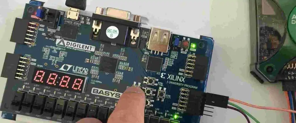
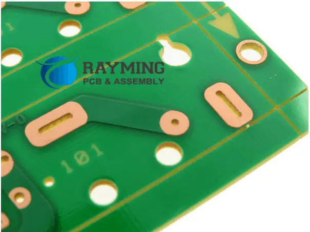
The application of solder paste is one of the most crucial processes in the SMT assembly. This process requires careful attention and a high level of precision. This is because the main goal is to apply solder in the proper location and adequately. Therefore, it is important to carefully coat each pad using the appropriate amount of solder.

The most common method integrated is screen-printing the solder paste. Solder printing is the most delicate step in the printed circuit board assembly. Printed circuit boards have defects due to the use of poor methods and tools for applying solder paste.  Solder paste containing lead are not RoHS compliant. It is advisable to apply lead-free solder paste on printed circuit boards.

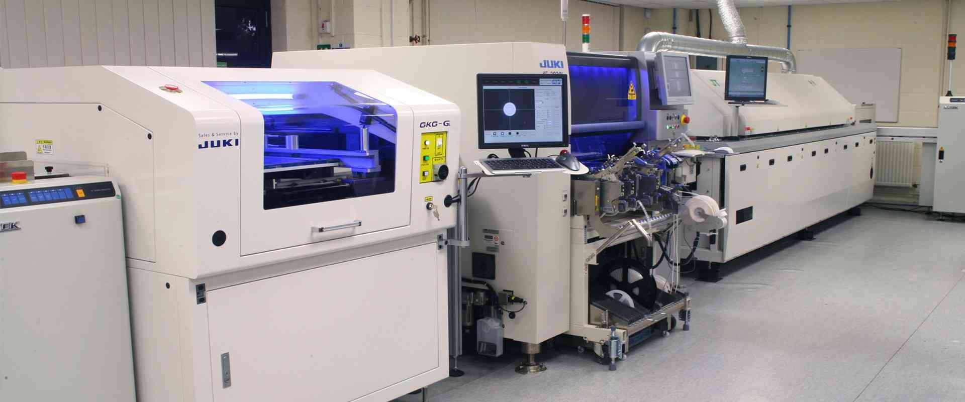
Rayming PCB makes use of automatic solder paste printers and a squeegee blade to apply solder paste on a circuit board. Also, this PCB assembler ensures enough pressure is applied to completely cover the circuit board with paste by dragging a squeegee blade through the pcb stencil printer, which has been tailored according to the IPC-7525A. These blades are typically made of metal. Here is a list of the key elements that determines effective solder paste printing.

What to Consider During Solder Paste Printing

smd soldering paste

Squeegee Speed

The amount of time the solder paste has to “roll” in the stencil’s apertures as well as onto the PCB pads is determined by the speed at which the squeegee travels.  The standard setting is 25 mm every second, however, this varies according to the aperture size within the solder paste and stencil used.

The Squeegee Pressure

To guarantee a thorough wipe of a stencil throughout a print cycle, it’s critical to apply enough pressure over the whole length of your squeegee blade.  Inadequate pressure might lead to incomplete transfer into the PCB, inadequate deposition, and “smearing” of that paste onto the stencil.  When there is too much pressure, this can cause paste “bleeding” between the PCB and stencil, “scooping” paste from bigger apertures, and too much wear from the squeegees and stencil.  A normal setting for the pressure of the squeegee is 500 grams for every 25mm of the squeegee blade.

The Squeegee Angle

Those holders to which the squeegees are attached usually set their angle at 60 degrees. If there is an increase in angle, the solder paste deposited will be minimal since the paste will be “scooped” out of the stencil apertures. Any reduction in the angle may result in solder paste residue remaining within the stencil once the squeegee concludes printing.

Speed of Stencil Separation

The speed of stencil separation describes the rate at which the circuit board gets separated from its stencil.  The apertures’ size within a pcb stencil printer will determine the speed setting, which can range from zero to three millimeters per second.  If this happens too quickly, the solder paste won’t completely release from these apertures, and “dog-ears”โ€”high edges surrounding the depositsโ€”will appear.

Cleaning the Stencil

Cleaning the stencil needs frequently is recommended while it is being used; the PCB assembler can perform this manually or mechanically.  A good number of automatic printing devices feature a system you can configure to clean a stencil using lint-free material and a cleaning agent such as IPA after a using a certain amount of prints.  The system executes two main tasks which is it cleans the stencil’s underside to prevent any form of smudging, and again it makes use of suction to clean off the apertures to prevent any form of obstructions.

Squeegee and stencil condition

soldering flux paste

It is important to carefully maintain squeegees and stencils since mechanical damage to any of these tools can lead to unintended effects. You need to thoroughly inspect  both of them before they are used and as well ensure they are cleaned, ideally with an automatic cleaning system which can get rid of any residue of the solder paste.  In case of any damage to squeegees and stencils, replacement must be done as soon as possible. This helps to guarantee a dependable and reproducible procedure.

PCB Support

It’s crucial to have PCB support so that the circuit board stays flat on the stencil during printing.  The poor paste deposits as well as smearing can occur during printing when the PCB isn’t adequately supported..

To maintain a uniform process, circuit board supports are typically included with the printing machines. These supports are fixed in height and feature programmable settings. Additionally, there are available adjustable PCB supports with a variety of designs that conform to the circuit board and are very important for two sided assemblies.

The Print Stroke

The squeegee should be at least 20 mm beyond the farthest aperture when traveling this distance through the stencil.  As the bead of the solder paste rolls on its return stroke, creating a downward pull that forces the paste through the apertures, traveling past the farthest aperture is crucial for allowing adequate room for the rolling of the paste.

Type, Handling, and Storage

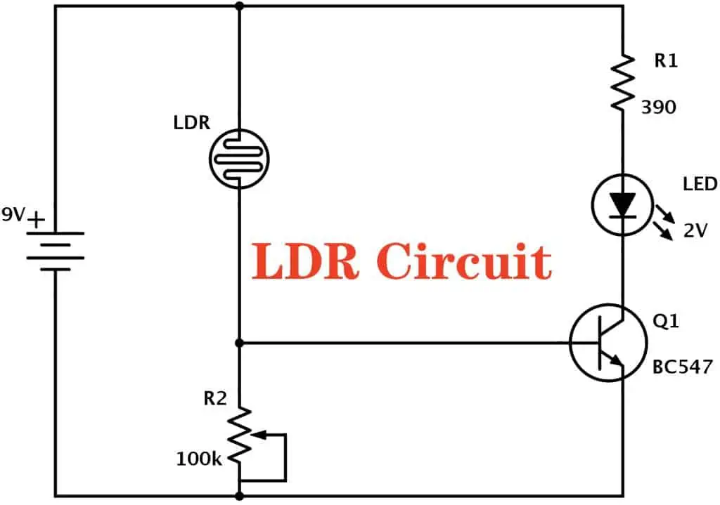
Solder paste is a combination of solder and flux. The components are held in place by the flux, which serves as temporary adhesive, until the soldering process melts that solder and creates the mechanical/electrical connection.

Because solder paste constitutes a ‘Thixotropic’ substance, energy is needed to alter its flow and viscosity uniformly through these stencil apertures. This energy comes from the velocity of the print head. The solder paste’s ‘Rheology’ is a term that describes how this solder paste creates a block without the application of energy but changes into a material which is more fluid whenever there is application of energy.

The apertures’ size within a stencil should determine the appropriate solder paste type to use.  The chosen solder paste’s particle size has an impact on the release of the stencil’s apertures.

According to the “5 ball rule,” at least 5 solder particles should be able to span the smallest aperture’s width. You need to keep the lead-free and tin-lead solder paste at room temperature for at least eight hours before the usage in order to retain quality. To extend the solder pasteโ€™s shelf life, you need to keep it chilled.

For uniform distribution of every separated material within the paste, the solder paste needs to be mixed before its use.  You can mix the solder paste either manually or mechanically with the help of the paste conditioner machine. Ensure you mix for a period of three to five minutes.

Solder paste should generally be thrown away after being used for more than eight hours.  However, you can keep solder paste at room temperature after being used for a maximum of four hours. Such solder paste can be kept in a sealed container before reuse up to a day.

Visualization (2D and 3D)

Automatic inspection may be utilized to precisely check the deposits of the solder paste to validate the procedure. ย There are also two kinds of inspection for solder paste. These are 2D inspection, that examines the paste deposit’s area, as well as 3D inspection, that examines the paste deposit’s volume.

What Varieties of PCBs may be Printed?

FULL PCB MANUFACTURING Quote

Irrespective of the type of PCB, whether rigid-flex, IMS, rigid, or flexible, if the strength of the circuit board canโ€™t hold the PCB perfectly and as necessary on the surface mount lines, the circuit board assembly manufacturer would inquire if the carrier (Durostone made) or SMT carrier can be customized.

It is based on the quantities used in PCB assembly.

To make sure the printed circuit board is flat on the stencil throughout printing, this is a crucial factor. Printing flaws such as poor paste deposits as well as smearing can result from a PCB that doesnโ€™t receive adequate support, regardless of whether it is rigid, IMS, rigid-flex, or flexible. To maintain a consistent process, PCB supports are typically included with printing machines. These supports are fixed in height while offering programmable settings. For double-sided assembly, flexible PCB are also available and helpful.

Solder Paste Inspection with Printing

Solder paste inspection  is necessary after applying solder paste on a board.  Errors can occur during the application of solder paste on a circuit board. The rule of thumb here is to fix a defect on time before it becomes more expensive. Early detection of errors in solder printing can help to prevent further errors.

A helpful rule to keep in mind is that a problem discovered after reflow would cost ten times as much to rework as one discovered before reflow, and a fault discovered after test would cost an additional 10 times as much.

It is acknowledged that there is more possibility for flaws or errors to occur during the process of solder paste printing. Also, the complexity of the printing process has increased with the use of small components and this has resulted in the use of lead-free form solder paste. According to experts,  tin lead solder pastes spread and offer more wettability  than lead-free form of solder pastes.

Generally, a lead-free technique necessitates a more precise printing procedure. The manufacturer has been compelled by this to execute some sort of post-print examination. Automatic inspection of the solder paste could be used to precisely check the deposits of the solder paste in order to validate the procedure. At RayMing PCB, we can identify a number of solder paste printing defect such as missing solder paste, the paste offset, spreading, bridging, and lines with insufficient or excessive deposits.

Printing using Low Temperature Lead-Free Solder Paste

To get a consistent, high-quality print while printing lead-free low temperature solder paste, it’s crucial to employ the right machine parameters. As previously mentioned, the standard print speed is 25mm for each second, and the standard squeegee pressure is 500 grams for 25mm of the squeegee blade.

If not configured properly, the settings enabling printing lead-free low temperature solder paste could be extremely different and result in smudgy prints. Printing at speeds of 50 to 100 mm every second should be substantially faster than with traditional solder pastes.  This setting should be closer to a pressure of 300 grams for every 25mm of the squeegee blade. The squeegee pressure has to be lower than typical solder pastes and it is advisable to utilize no additional pressure than necessary to get the clean stencil during printing.

The quantity of the solder paste applied to a stencil should also be considered. Since the stencil it is lighter weight and has less tin than lead-free low temperature solder paste, it can adhere to squeegee blades while it is in use.  In order to make the paste remain within the stencil inside the continuous bead, ensure you apply more paste compared to ordinary solder.

An increase in productivity and efficiency

It’s surprising that several surface mount processes within our electronics industry, especially those in subcontract manufacturing, operate at as little as 20% in terms of efficiency. This percentage is because of the various factors. However, it basically indicates that just 20% of this capital invested is being used.  As regards financing, there is more ownership cost, and also a lower rate of return on investments.  There may be a longer lead time for the customerโ€™s products and as a result, the company won’t stay competitive within the market.

The firm will be impacted by a number of consequences when there is a low level of production efficiencies.  This includes more batch sizes, additional components in stock, extra assemblies in progress, as well as slower response times to modification requests by customers.

With all the factors mentioned above, there is a reason to increase efficiency while still ensuring quality.

Conclusion

Solder paste printing is a crucial step in the PCB assembly process.  When there are defects at this point, there’ll be “knock on” consequences all through the process. Therefore, all components of the process described above must be looked into so as to achieve an ideal solder paste printing procedure. You can determine the quality of solder paste by carrying out a coalescence test . This test can also help to determine how the working atmosphere (relative humidity and ambient temperature) would have an impact on performance.

What is a Timer Switch Circuit? Its Types and Application

Timer Switch

A timer switch simply refers to a type of device that turns the power on and off at a specific interval of time. However, most people think like that about timer switches. They not only turn on and off the device but also provide various options to control the timing and schedule it.

This article gives you a detailed insight into how a timer switch works its different types, features, benefits, and disadvantages, along with its usage.

What Is A Timer Switch Circuit?

A timer switch circuit refers to a type of timing device. It operates on both electrical circuits and mechanical circuits. This type of device controls the time of the device when turning it on and off. However, to understand it better, read on next.

YouTube video

Definition of Timer Switch Circuit

A timer or time switch is also known as just a timer. As the name suggests, it controls the time intervals of a device that turns the power on and off on the preset schedule or time. It mainly operates on either electrical or mechanical processes based on device usage.

It is a type of plug that one can easily plug or install inside the wall. Regardless of its type, one can use it either outdoors or indoors. Some basic applications include street lights, AC symptoms, sprinkler systems, and security system lights.ย 

Functions of Timer Switch Circuit

Timer Switch Circuit

The main purpose of a timer switch is to eliminate the need to manually switch on and off electrical devices. Moreover, it also saves money and consumes less power. It is mainly responsible to turn on the device at a specific time and turn it off without concern. Moreover, it gives you a sense of security as you donโ€™t need to worry about turning on or off the lights while you are not at home. It automatically turns on the scheduled light and pretends that you are at home. 

Additionally, it offers a great sense of auto-control of smart houses through customized wireless control options. Thus, leaving your worries away and keeping you safe and sound.

Symbol of Timer Switch Circuit

The electrical symbol of the timer switch represents an SPST switch type. The SPST stands for Single Pole Single Throw. It also contains a timing sign over it. This, however, makes the process easy to identify the symbol of the timer switch in a circuit diagram. For instance, the timer switch symbol may look like an on-and-off switch, along with a sign of a timer over it in a circuit layout diagram. This timer symbol shows that it is not a simple on-and-off switch despite it being a timer switch. 

Types Of Timer Switch Circuit

Timer switches come in various types and forms. Each type offers its own features along with drawbacks. However, four basic timer switch types include mechanical, electronic, photocell, and astronomic timer switch. 

ยท Mechanical Timer Switch Circuit

An Analog timer also refers to an automatic and mechanical timer switch. This is one of the most common and widely used timer switch types. It contains mechanical components such as gears and springs. These help in setting the time. Moreover, it contains a knob that needs manual setting adjustments to control the turn on and off of the power. 

However, mechanical timer switches come with both benefits and drawbacks. It offers benefits that include easy usage and low cost, whereas it’s not lightweight. It contains moving parts that increase maintenance time, cost, and care.

ยท Digital Timer Switch Circuit

Digital timer switches also refer to electronic timer switches as they operate on the electric current both in AC and DC form. They contain a microcontroller which implies that they do not have any moving or mechanical parts. Moreover, it also contains a button that helps in changing the time setting with a button at any time. This feature helps in quickly setting the daily time intervals of when to turn on and off the device. 

 In addition to this, these types of switches also give accurate and precise results, which makes them ideal to use in various applications. Moreover, they also support custom settings as per the users’ needs. 

ยท Astronomic Timer Switch Circuit

An astronomical or astronomical timer switch operates on the sunโ€™s position and sets the turn on and off timing according to it. An astronomic timer comes in digital form. It basically consists of built-in memory that stores the program. This program contains all the information on when to turn on and off the device.

More specially, this data includes the latitude, longitude, and location-related data of the device. This data helps the timer to analyze the accurate time of when the sun rises and when it sets and runs the device accordingly. Hence, it then helps the device to turn on and off at certain times of day and night according to the sun’s position. Moreover, it operates with immense accuracy.

ยท Photocell Timer Switch Circuit

A photocell, as the name suggests, is a type of timer switch that operates in the presence of bright light. This type of timer is used in a situation where devices need to control the turn on and off setting through light. Photocell timer switches use photodetectors or optical sensors to sense the light. This simply turns on the device in the dark, whereas it turns off the device when the light falls on it. This type of timer switch is used in devices like street lights and home, office, and buildings security lights.

How Does A Timer Switch Circuit Work?

FULL PCB MANUFACTURING Quote

Letโ€™s dive into the details of timer functioning. However, to understand the working principle of timer switches, letโ€™s look into its two main kinds. Electronic and mechanical timer switches work in different ways.

ยท Mechanical Timer Switches

A mechanical timer switch works in an analog form. It uses a clockwork process to control and manage the time when to switch on and off the power supply. This type of timer switch contains a knob. This knob helps in programming the required time on which the power will turn on and off. 

A mechanical timer is also referred to as an analog timer. It can easily adjust the turn-on and off settings manually. As it does not have any memory, it needs manual adjustment each time.

ยท Electronic Timer Switches

An electrical timer switch belongs to a digital sort of switch. It uses microprocessors and an internal clock to control and manage the turning on and off of the power supply. This type of timer switches programs earlier on the basis of time intervals in seconds, minutes, hours, and days. 

Moreover, the electrical timer offers various other features. These features include randomization settings. This setting changes the time daily to prevent the burglars from realizing the switch patterns. In addition to this, it also has a digital screen which helps in viewing and programming the required settings.

Conclusion

You may know now how versatile a timer switch can be. It serves as a special device that helps in controlling different types of electrical circuits in homes, offices, common areas, commercial places, and industrial environments.

It provides convenience, security, and energy efficiency. Moreover, it gives you full power to control and schedule the turn on and off of devices like Air conditioners, pumps, and lights.

A Comprehensive Overview of Encoder Circuit

An encoder refers to a type of digital circuit. It takes input in binary forms and converts it into binary code. Here, a binary code refers to the input position and identifies the active input. Encoders are widely used in digital devices to convert a set of parallel inputs into a set of serial codes of output. 

An encoder follows simple basic functional principles. It assigns a unique binary value to every input value. For instance, an encoder with 2-4 lines contains two lines of input and four lines of output. However, it assigns a unique binary code of 4-bit to both inputs with a combination of 2 exponents of 2 = 4. This encoder output usually comes in active low form. This means that it only gives one active low output at any specified time, whereas it gives inactive high output the rest of the time. The value of active output selects on the basis of the binary digits which assigns to an active input.ย 

YouTube video

Encoders come in various types of forms. Some include priority encoders and binary-weighted encoders. Priority encoder sets a priority value for every input, whereas binary encoders use binary codes as inputs. In simple words, encoders refer to a type of digital system or circuit that uses binary inputs and converts them into a unique code of binary that represents the input location or position. 

An encoder is a reverse logical circuit of a decoder. It contains a max line of input as two exponents of n and gives n number of output lines. Thus encoding the two exponents of n input value into an n number of output code. It generates a high active input in binary code corresponding to the input. Hereby, it encodes the two exponents of n lines of input in n number of output bits.

Types Of Encoder Circuit

Encoder Circuit schematic

Encoders have various types. Some of them include:

1. 4 to 2 Encoder Circuit

The Encoder 4 to 2 contains four inputs and two outputs. The input includes Y0, Y1, Y2, and Y3, whereas the output includes A0 and A1. here only one of the four inputs can have a โ€˜1โ€ value to get an individual output binary code.  

2. Octal To Binary Encoder Circuit

This encoder is octal to binary and contains eight inputs and three outputs. The inputs include Y0 to Y7, whereas the output includes A0, A1, and A2. In this, each line of input corresponds to 8 digits and gives three binary ode outputs.ย 

3. Decimal To BCD Encoder Circuit

The encoder decimal to binary contains ten lines of inputs and gives four lines of outputs. In this, each line of input contains the decimal numbers, which gives four outputs in the binary code format. However, this encoder allows the input value in a decoded decimal digit, which encodes them into output binary code digits in the lines of output.

4. Priority Encoder Circuit

The priority encoder contains four inputs. These inputs include Y0, Y1, Y2, and Y3. it gives two outputs which include A0 and A1. In this, Y0 input contains the lowest input priority while Y3 contains the highest input priority. Here the input value has more โ€˜1โ€™ simultaneously; then, the output comes in the binary code, which corresponds to the value of the input that has the highest priority. 

People have to go through some errors while encoding the process. At the same time, some common errors include the following. When the value of all output comes to zero, it becomes complex and gives errors. Moreover, if the value of the input is High and comes twice and greater, then it creates an output that contains an error in the code. 

However, to resolve these issues, make sure to set priorities for every encoder input. Thus it gives the value of the output code that corresponds to the value of the input with high priority.

Applications Of Encoder Circuit

Encoders serve as electrical circuit that is widely used in almost all types of digital systems. Encoders mainly use to convert decimal numbers into binary numbers to execute binary functions. These binary functions include division, multiplication, subtraction, and addition. Moreover, it is also used in applications that need to detect the interruption in the microprocessor.ย 

Advantages Of Encoder Circuits In Digital Logic

ยท Reduction In The Number Of Lines

Encoders minimize the number of lines that need to transfer data from multiple signals input into one output value. However, simply changing the design reduces the component cost.

ยท Improved Reliability

Encoders can convert multiple input signals into just one serial code output. This enables the encoders to prevent errors during the data transmission.

ยท Improved Performance

Encoders reduce the input transmission time from various inputs to one output value. Hence automatically enhances the digital system performance. 

Disadvantages Of Encoder Circuit

FULL PCB MANUFACTURING Quote

ยท Increased Complexity

Encoders seem simple circuits but come with more complexity than other multiplexers as they need additional types of components to execute.

ยท Limited To Specific Applications

Encoders can only be used in a type of application where a set of parallel inputs needs conversion in a serial code format.

ยท Limited Flexibility

Encoders have fixed flexibility. They only encode a limited amount of input numbers into a limited amount of output values.

Encoder Vs. Decoder

The Encoder circuit converts the analog or digital signals input into the binary-coded output format. Encoder uses an OR gate to convert the data into coded form. Moreover, encoders also accept input in โ€˜2 with an exponentโ€™. Encoder uses input in the form of analog and digital signals. Moreover, it is a simple process.

Whereas the decoder converts back the coded binary numbers into their original signal format. It uses basic logic gates like NAND or AND gates. It converts the binary digits from n input lines into a max 2 with an n exponentโ€™s output line. Decoder uses input in the form of coded binary digits. Moreover, it is quite a complex process.

Conclusion

Encoder is a special type of digital circuit. It comes with various types of features as well as disadvantages. However, using an encoder in the device depends on the system’s requirements and usage. Moreover, factors like cost, performance, reliability, and complexity also depict whether to use it or not. 

Whereas decoder and encoder refer to logic circuits. However, both differ in performing their functions. The encoder encodes the signal data while the decoder decodes the data of the coded signal to get the exact message. Besides this, both the decoder and encoder offer various other beneficial features.

The Essential Guide to LDR Circuit (Light Dependent Resistor) & Its Working

ldr circuit

Sometimes, home appliances and lights need to operate and controlled manually on various occasions and events. However, human negligence and unwanted situations may lead to power wastage of appliances. Therefore, to control the situation, engineers provide a better alternative to control.

LDR, which refers to Light Dependent Resistor, helps in controlling loads of the circuit based on light intensity. LDR also serves as a photoresistor device that comprises semiconductor material of high resistance.

This article gives you a detailed insight into LDR, its functioning, working principles, types, as well as advantages and disadvantages.

YouTube video

What Is an LDR Circuit (Light Dependent Resistor)?

LDR refers to an essential electrical component of a circuit that responds to light. It changes the resistance as the rays of light fall on it. The value of resistance of the LD resistor changes many times. However, the value of resistance drops immediately as the level of light increases.

The LDR resistance value may vary in darkness and bright light. It gives several Mohms value in darkness, yet it decreases to a few hundred ohms in bright ray light. This change in resistance makes LDR be used in various types of applications and devices. Moreover, the sensitivity of LDR also alters through the wavelength of incident light.

Semiconductor materials have light-sensitive properties. Therefore, designers use semiconductor material in LDRs because of this feature. Cadmium sulfide is a widely used material for the composition of LDRs. At the same time, some European countries restrict the use of this material along with Cadmium Selenide because of environmental concerns. Moreover, they can use Indium antimonide and Lead sulfide.

Resistors use semiconductor material because they do not contain any PN-junction and act as passive devices. Therefore, simple resistors do not fall into the category of LDRs like photodiodes and phototransistors.

LDR Circuit Symbol

LDR Circuit schematic

The LDR symbol basically represents the symbol of the resistor in electronic PCBs. However, it may describe the rays of light in the form of arrows. This way, the LDR symbol follows the same principle as the photodiode and phototransistors symbol, in which arrows illustrate the drop of light over the components.

Construction Of An LDR Circuit

The fabrication of LDR contains light-sensitive or semiconductor material which is placed over the ceramic for insulation. Designers put the material in a zigzag form. This gives desired resistance and power rating. The zigzag area is distinct from the area of metal-placed in two separate spaces.

On both sides of the surface, it creates ohmic contacts. Here, designers keep the resistance low as much as they can to ensure that resistance only alters over the light. Moreover, they avoid using cadmium and lead semiconductor materials as they affect the environment. 

Working Principle Of Light Dependant Resistor

The LDR working principle follows photoconductivity which represents an optical function. The material conductance enhances as the light falls on it.

Whereas, when it falls over the LDR, the electrons present in the material valence band start tending to the conducting band. But the incident ray light has photons that carry superior energy to the material band gap. This enables the electrons to jump from the valence band to the conduction band.

Moreover, when light contains ample energy, it excites more electrons to a conduction band. Whereas, when current flow and process effect start increasing, it automatically decreases the device resistance.

Light Dependant Resistor Circuit

The LDR circuit consists of LDR, diode, resistors, and Darlington pair. In this voltage supply connects with the load. A battery or a bridge rectifier is used to provide Direct Current voltage to the circuit of LDR. Moreover, the bridge rectifier utilizes a step-down transformer for voltage step-down from 230 to 12 volts. Diodes are connected in a bridge that alters the Alternating Current-voltage into Direct Current.

It also uses a voltage regulator, which helps in changing the DC-DC, 12-6 volts. This current then goes to the whole circuit. An AC supply of 230 volts to both the load and bridge rectifier. Moreover, ensure to keep them constant for light-sensor type circuits. 

This sensor shows low resistance in the daytime, around 100 ohms. Hence, the power flows across the LDR and ground going through resistors and variable resistors. This happens because of LDR. During day time when light drops over the LDR, the resistance decreases as compared to other parts of the light sensor circuit. As we know, the current always goes through the path of less resistance.ย 

Therefore, they really do not provide enough power supply. Thus turning off the light in daylight. Similarly, the LDR resistance increases at night time by about 20 megohms. Because of high resistance, current flow decreases and gets zero. Here, current flows through the path of low resistance, which increases the Darlington pair base voltage up to 1.4 volts. The Darlington pair then provides enough power supply to the relay, which turns on the light at night time.ย  ย  ย  ย 

Frequency Dependence of LDR Circuit

FULL PCB MANUFACTURING Quote

The LDR sensitivity depends on the wavelength of the light as it affects the responsive area of a device. However, this effect can be easily found and noticeable when the light wavelength goes outside the determined range. After this range, one cannot see the effect. Different types of material in the device react and respond differently to the light wavelength. 

Moreover, extrinsic resistors type respond more quickly to the wavelength of light as well as IR. But make sure to take precautionary measures for dissipating heat released from IR while working on it.

Latency of LDR Circuit

LDR is highly associated with an important factor, latency. Latency depicts the time required for responding to any changes in the components. Therefore, these features make it important to consider while designing a PCB. Latency shows the time at which a person can easily see a note. This time refers to changes that LDR attains from one light level to another light level. Therefore, LDR does not fit well for devices where light changes its value quickly. If the occurrence of light changes remains for quite a time, then it pars the sufficient level.

The resistance recovery rate determines the rate of change in resistance. Generally, LDR responds to the light in a few mili seconds after thorough darkness. After that, the time limit rises to a second. However, in the datasheet of components, the specifications of LDR are written as the resistance to darkness after a certain time, such as in seconds. The most used quoted values are 1 and 5 seconds. These values clearly indicate the latency of a resistor. 

Types Of LDR Circuit

LDR has various types based on the material’s photosensitive and linearity. LDR uses different types of materials. These include lead sulfide, cadmium selenide, thallium sulfide, and cadmium sulfide. 

LDR that comprises cadmium sulfide proves responsive to almost all sorts of light radiations and rays a human can see within their spectrum. However, LDR that comprises lead sulfate can only respond to Infrared radiation.

Based on the types of materials and their photosensitive ability, LDR divides into two types: Linear LDRs and Non-Linear LDRs.

Linear LDR also refers to photodiodes. Due to its linear operation and performance, it serves as a photoresistor in several applications. Non-Linear Light Dependent Resistors are found more commonly in devices. However, polarity does not determine its function and operation, which unites it.

An Ultimate Guide to ยตBGA (Micro Ball Grid Array)

ยตBGA

The ยตBGA or Micro BGA or Micro Ball Grid Array is considered among the latest and most advanced Surface-mounted devices, which quickly turn into a package for PCB designers. A micro Ball Grid Array is a subcategory of a general BGA. The typical ball-to-ball spacing of the BGA package ranges between 0.8mm and 1.0mm, whereas the pitch of the general package of micro BGA ranges from 0.4mm or may be less than this. However, this minimizes the size of the package. Additionally, a micro BGA can also be placed in very close proximity to the surface of a PCB.

The technology of packaging plays an essential role in the performance of a device. In the last few years, advanced technologies have lessened the delay of chips in an actual Integrated Circuit semiconductor substance. Although, the signal delay cannot reduce much in an IC of a package. Hence, packages become an integral part of high-speed performance devices. Micro BGA serves as an ideal solution, among others. Because it allows greater chip delay activity than other technologies.

ยตBGA (Micro Ball Grid Array) Defect Inspection 

BGA Chip

After the soldering process, the component of BGA can easily be detected. However, the component, equipment, soldering process, and environmental issues may create defects. These defects may include open circuits, cold soldering, short circuits, bridging, loss soldering, and misalignment. Nevertheless, sometimes the BGA solder balls contain defective problems like missing balls and uneven sizes.

The BGA inspection may cause difficulty in judging the high quality of the final product. It is associated with the fact that solder balls of BGA are placed beneath the visual inspection and the chip. This, however, is not able to show the cavities available in the solder joints. Therefore, the inspection demands professional and sophisticated inspection equipment that gives quality results. Such advanced methods include boundary scans, X-ray inspections, and electrical tests.

The traditional ways of electrical testing prove ideal for detecting short and open circuits. Whereas the boundary scan aids in accessing solder joints, there they make a connection which is called boundary connectors. This allows you to inspect short and open circuits over the connected SMD components. The method of boundary scan also allows the testing of invisible and unseen joints more than the electrical tests. Both prove effective in inspecting the electrical performance and conduction of a board. However, they cannot inspect the solder quality. Therefore, you must incorporate other methods with these technologies that help in finding the solder quality as well as the solder present in hidden and invisible joints.

The X-ray machine method carries out other defects that are created during the assembly of BGA PCB. The X-ray inspection eliminates soldering issues like solder balls and pastes bridging. Though, some X-ray machines contain software support that can easily compute gao size in a solder ball. This, however, ensure that the X-ray machine must follow the standard set. A 2D X-ray machine helps in generating 3D images to analyze inner layers, cold soldered joints, blind vias, and vias on the soldered joint of a BGA.

Benefits Of ยตBGA (Micro Ball Grid Array)

Because of the complex structure of the ยตBGA package as compared to other surface-mount devices, it possesses a smaller contact length between the pin of the device and the outer world. However, it gives a low impedance and inductance path to each signal. Along with technologies of logic implementation and the advancement of Integrated Circuit semiconductors, it keeps pace and minimizes the loss of signal by enhancing the density of packages and reducing the delay in the packaging process.

The electrical performance of a ยตBGA represents that it was apple or resistance, inductance, and capacitance of shorter leads. For devices with high- performance, an additional ground plan then minimizes the mutual and self-inductance and crosstalk.

Whereas micro BGAs indicate a major advancement in the packaging of components as they create greater challenges for PCB layout. A general micro or ยตBGA package comprises a pitch of 0.4mm, while the advanced clear-pitch BGA comes in smaller pitches like 0.25mm and 0.3mm. Designers of PCB need to find easier methods and solutions for pin routing with a BGA pitch of 0.4mm; otherwise, it may result in routing complications. Eventually, those complications result in increasing the layer count along with high requirements of the fabrication process. This implies that before using a design for a microBGA package, designers need to analyze the details of the device of microBGA carefully. It also ensures that the pin pitch of a ball allows the routing of all traces without using unwanted special requirements of manufacturing. Additionally, this process can be carried out within the desired layer counts.

However, this shows that designers want to optimize the layer count needed for routing packages of greater pin count without importing their performance. Moreover, the pin grounding and assignment of a microBGA may be easily modified to allow efficient routing along with an optimal number of board layers.

NSMD & SMD Pads Of ยตBGA (Micro Ball Grid Array)

FULL PCB MANUFACTURING Quote

The manufacturer of chips has detailed information sheets which consist of land patterns. BGA pads typically have two kinds of surface patterns. Solder Mask-Defined or SMD pads and Non-Solder Mask-Defined or NSMD pads. 

The NSMD pads contain openings of solder masks. These openings are larger as compared to the pads. At the same time, the SMD pads contain openings of solder masks. These openings seem smaller as compared to the pads of copper. The majority of suppliers suggest using NSMD as it gives stronger control of the artwork registration of copper than the process of solder mask positional tolerance. Therefore, this becomes even more essential when PCB designers work with clear-pitch components such as the ยตBGA package.

ยตBGA (Micro Ball Grid Array) In PCB Design

The routing or fanout technique considers a few aspects like surface diameter, ball pitch, via type, size of the pad, layer count, trace spacing or width, and the number of input/output pins needed to get away from micro BGA.

A conventional dog-bone routing pattern does not seem appropriate for the micro BGA. This enhances the need for buried/blind via or via-in-pad. The method of via-in-pad puts a direct via beneath the contact pads of the device. These vias are filled with either conductive copper or other conductive material like silver. Thus providing a flat surface. This improves the routing and gives high density to the components.

It clearly shows that the traditional method of BGA routing does not work here. This implies that the manufacturer has to use either buried/blind vias or via-in-pad or maybe both. However, do not use buried or blind vias if you really want to make the manufacturing process of PCB cost-effective. Although, it is truly based on the size of the micro BGA and the arrangement of pins.

The package of micro BGA enhances the complexity of the design. The narrow pitch of the package creates various challenges in the design of PCB because of placing a larger number of component pins within the design of a compact area than a traditional BGA. In the same manner, the fabrication of the board has to go through advanced techniques and methods, which increases the cost. The PCB manufacturers need to create a simple fabrication process of a PCB for such types of components and must consider placing pitch components.

The Micro BGA offers various physical and electrical benefits. Moreover, like every other technology, a micro BGA also does not come without issues. For instance, no one can find expertise like micro BGA easily or commonly. The method of rework gets more complicated, while the reliability of the solder joint is even more critical. Additionally, voiding is becoming a fast-growing issue, whereas the assembly inspection of micro BGA also gets difficult.

Why is Xilinx XC7A50T-2CSG324I FPGA needed for Next-generation applications?

Xilinx Zynq

Applications are those modern applications that use technology. They necessitate rapid data processing, minimal latency, and low energy consumption. These types of applications are developed to manage colossal volumes of data while delivering real-time outcomes. Some examples of next-level applications include artificial intelligence, machine learning, 5G wireless networks, field programmable gate array, and IoT or the Internet of Things. Similarly, The Xilinx XC7A50T-2CSG324I is a cutting-edge Field-Programmable Gate Array (FPGA). It is designed to cater to the demands of the coming generation’s applications. FPGS are used in a plethora of sectors, such as aerospace, industrial, automotive, medical, and telecommunications. It’s all because of their dynamic architecture, modifiable design, and low power usage.

The following content will take you deep into the Xilinx XC7A50T-2CSG324I’s prime features. It will also explain to you how it is propelling the next-generation applications. First of all, you must have some basic information regarding Xilinx XC7A50T-2CSG324I.

What Is the Xilinx XC7A50T-2CSG324I and Why It Is Famous for?

Xilinx Virtex-5 fpga

The Xilinx XC7A50T-2CSG324I belongs to the Xilinx 7 series of FPGAs, which utilize a twenty-eight-nanometer blueprint. It is an exceptional apparatus that encompasses a dual-core ARM Cortex-A9 processor coupled with a vast array of configurable logic blocks and input/output resources.

The XC7A50T-2CSG324I has a highly flexible design. That’s why it allows for a broad spectrum of customization options. You can easily customize it to match a specific application’s needs. It includes image and signal processing, control systems, and high-speed data transfer.

Reasons to tell you why Xilinx XC7A50T-2CSG324I is the need of future

1. High-Performance Architecture with Real Time Processing

ย The Xilinx XC7A50T-2CSG324I boasts a high-performance architecture incorporating a dual-core ARM Cortex-A9 processor. Its high-speed configurable logic blocks are just icing on the cake. They can deliver exceptional processing power and performance. As a result, its real-time processing capabilities make it an excellent fit for high-speed data transfer. In addition, it takes less time compared to the microcontroller. Video and image processing applications also have XC7A50T-2CSG324IPower efficiency.

2. Great Energy Efficiency

This FPGA has the best features and great applications. Despite the outstanding architecture, the Xilinx XC7A50T-2CSG324I is energy efficient. Yes, it is a great plus point. This FPGA prioritizes energy efficiency. It has refined power management capabilities. ‘s why it enables it to work at low power levels without impeding its performance. Yes, impedance is the biggest issue when it comes to power management. Micro controls find it hard to deal with impedance. This makes it the best option for low-power-consuming applications. Low power-consuming modern devices such as battery-powered devices and embedded systems have XC7A50T-2CSG324I.

3. Flexibility For Better Customization

Previously micro, microcontrollers were pre-programmed, that’s why it was hard to program them. The Xilinx XC7A50T-2CSG324I exhibits remarkable flexibility. You can easily customize it according to your needs.

 It has a range of customization options. That’s why it is easy to be programmed according to the needs of a particular application. It has a fair number of logic blocks, that’s why it is easy to program it. It also has a myriad of input or output resources. As a result, it is easy to match it with a different application. The good thing about this FPGA is greater customization. Yes, you can program it according to design and need. That’s why it is ideal for different applications in different fields. Xilinx XC7A50T-2CSG324I FPGA is the need of modern next-generation applications due to its customization. Every time when you use it on the device, then you can easily integrate it into the new application.

4. Next Level Scalable Performance

 The Xilinx XC7A50T-2CSG324I offers scalable performance. All modern next-generation devices may show varying degrees of proc. It has the ability to use power and performance. That’s why this FPGA can serve better. It has the ability to take performance to the next level. It is easy to work with different devices that provide diverse levels of performance and functionality. That’s why it is easy to integrate it with systems for automation; as a result, it shows better performance and better efficiency.

5. User-Friendly Features And Interface

The Xilinx XC7A50T-2CSG324I’s advanced capabilities do not compromise its user-friendliness. It has an array of development tools and software that simplifies the programming process. It has a user-friendly interface. Even a hobbyist can easily use it if you have a fear of not handling it properly. You can take help from the community. There are several online tutorials regarding Xilinx XC7A50T-2CSG324I FPGA. That’s why it is the need of all contemporary hi-tech applications.

Are There Any Development Tools Available For Xilinx XC7A50T-2CSG324I?

Xilinx provides a range of development tools for all of its FPGAs. When it comes to Xilinx XC7A50T-2CSG324I, then again, there are different tools. Vivado Design Suite and the Xilinx SDK are at the top of the list. That’s why it is easy to program and reprogram this FPGA. These tools have exceptional features that are why designers andย developersย can design, simulate, and debugย Xilinx XC7A50T-2CSG324I.

How Is The Xilinx XC7A50T-2CSG324I FPGA Better As Compared To The FPGAs In Its Class?

FULL PCB MANUFACTURING Quote

Xilinx XC7A50T-2CSG324I offers a good balance of performance and low power consumption. Although all FPGs show good performance, the XC7A50T-2CSG324I FPGA has a large number of I/Os and other peripherals. That’s why it shows better customization and better performance as compared to their FPGAs. If you want to use any FPGA, then compare it carefully. However, the specific choice of FPGAs depends on the application design and need.

 Wrapping Up

The XC7A50T-2CSG324I is a formidable FPGA. It has great potential to revolutionize the next generation of applications. Its exceptional capabilities and adaptability make it a versatile tool in various industries.  The technological advancements continue to accelerate at a breakneck pace; the need for high-performance FPGAs such as the XC7A50T-2CSG324I is expected to surge. That’s why we call it the heart of next-generation applications. Its cutting-edge technology and innovation are enough to make it part of the future application. If you are searching for a powerful and more adaptable FPGA for your next project, the XC7A50T-2CSG324I is undoubtedly a worthy consideration.

Let’s Explore XC7A200T-3SBG484E’s Specifications and Features

Xilinx Artix 7

FPGAs are emerging as a popular choice among hardware designers and engineers. These programmable offer a high degree of flexibility, scalability, and customization. That’s why they are suitable for a wide range of applications. You can find them in several applications, from aerospace to consumer electronics. Now, days every other sophisticated device has FPGA to enhance its working performance.

One of the most powerful and advanced FPGAs available in the market today is the XC7A200T-3SBG484E.  This FPGA has amazing features. It is a quality FPGA by Xilinx. You all know that Xilinx is a leading company in the FPGA industry.   This company is famous for its innovative and reliable products.

What Is XC7A200T-3SBG484E?

The XC7A200T-3SBG484E is a part of Xilinx’s Artix-7 FPGA family. This family is famous for low-cost and low-power applications. Moreover,  it is based on a 28-nanometer (nm) process technology. This latest technology enables it to deliver high-performance features.  In addition, it maintains low-power consumption. As a result it is ideal for compact and battery-operated devices.

This FPGA features a programmable Logic capacity of 215,360 logic cells, which makes it suitable for a wide range of applications. As a result, it offers high-speed processing and data transfer. It also comes with several built-in features and interfaces, such as gigabit Ethernet and PCIe. Similarly, it has Gen2 and high-speed serial transceivers to enhance its capabilities.

Let’s have a look at its specifications.

Key Specifications     

Xilinx FPGA Programming

 This FPGA comes in Package: of 484-pin ball grid array       

  • This FPGA offer Speed grade -3 
  • The operating temperature range is between -40ยฐC to +100ยฐC
  • It has 215,360 logic cells. These clues are the basic building blocks of this FPGA.      
  • It has 860,160 CLB flip-flops and 430,080 CLB LUTs
  • Block RAM of 5,040 Kb is just the icing on the cake.
  • 740 DSP slices make signal processing more convenient.
  • 32 Transceiver count is an added feature        
  • 400  user Input and output pins  
  • Core voltage 0.95V to 1.05V  is for this FPGA 
  • 1.8V is auxiliary voltage for it.  
  • Gigabit Ethernet and PCIe Gen2 interfaces

Unique Architecture And Design

The XC7A200T-3SBG484E has a highly optimized architecture.  As a result, it combines several advanced technologies to deliver maximum performance.  Its efficiency is unmatchable. It features a configurable logic block. That’s why it is easy to be customized and implement various logic functions. For example, it is ideal for arithmetic functions, memory, and combinatorial circuits.

This FPGA XC7A200T-3SBG484E also includes a variety of specialized blocks. For example digital signal processing blocks and memory blocks are some special blocks.    In addition Input and output blocks are just icing on the cake. That’s why it is easy to implement even complex functions and algorithm.  It also has a flexible routing matrix. It also supports different interfaces.  As a result, it allows designers to connect different blocks and modules.   In addition, it optimizes their design for specific applications.

Advanced Debugging And Monitoring Features

  • It has up to date debugging and connectivity features that make it ideal to use.
  • Integrated Logic Analyzer allows for real-time capture and analysis of signals within the FPGA fabric. The 
  • A logic analyzer can capture signals from up to 256 probes.  It offers a maximum frequency of five hundred MHz.
  • Integrated Memory Controller supports several industry-standard memory interfaces. For example DDR3, DDR2, and QDR II+.
  • Integrated PCIe Endpoint Block: This allows for high-speed communication with external devices. It is possible through a PCIe interface    
  • JTAG Boundary Scan is helpful for testing and debugging board-level connectivity issues.  In addition, it test and program the FPGA and its functionality.   
  • Power Monitoring allows designers to monitor the power consumption of the device and optimize their designs for power efficiency.
  • These advanced debugging and monitoring properties of the XC7A200T-3SBG484E FPGA make it eminent among all other FPGAs. If you are
  • Looking for debugging and security features, then this FPGA serves better.  In addition, it allows designers to quickly identify and correct issues in their designs.

Alphanumeric Breakdown Of XC7A200T

FULL PCB MANUFACTURING Quote

At first glance, you may consider these numbers and the alphabet as ordinary numbers. But these alphabets and numbers show significance. They have some meaning. Following the breakdown of these alphabets and numeric will help you to know about this FPGA.  XC is the prefix. Mostly   Xilinx uses it to identify their FPGA products. So if any FPGA name starts with XC, then, you can understand its manufacturer. 7A indicates that the FPGA is part of Xilinx’s Artix-7 family. Xilinx has different FPGA families, and FPGAs belonging to particular families has different specifications. That’s why it is necessary to

Know about the FPGA family.  As a result, you can easily understand the basic features of this FPGA.

  • 200 represents the number of logic cells in the
  • FPGA. In this case, these logic cells are 215,360. These building blocks make FPGA and you can’t expect any FPGA without it.
  • T indicates that the FPGA is a -3 speed-grade device.  In addition, it means it can operate at a maximum speed of 1.25 GHz.
  • 3S tells about the package type of the FPGA. That is simply a 484-ball, 0.8 mm pitch, BGA. BGA stands for ball grid array.
  • BG484 is the package code that identifies the physical Package and pinout of the FPGA. So without opening the Package, you can know about the product inside.  E indicates that FPGA is RoHS compliant. It means that it doesn’t conation lead or any harmful material

Wrapping Up The Things

Nowadays, most modern applications use the  FPGA due to its unique features. That’s why an FPGA is more sophisticated than any microcontroller. So go for any one of them by keeping your needs in mind. Above all, if you find yourself confused, you can seek professional or expert help. In our opinion, XC7A200T-3SBG484E has unique architecture and debugging features. That’s why designers that prefer superior architecture can go for it.  Above all it is good XC7A200T-3SBG484E FPGA.

Understand the Difference between OSP vs. ENIG Surface Finish for PCB: Which is Better?

OSP Vs ENIG

Printed circuit boards are now more crucial than ever due to their excellent properties. Today, you cannot think of developing consumer electronics without PCBs at all. However, it is obvious that the PCBs are building blocks of futuristic electronics on all counts.

 It means these have to be faultless as well. Or else they will fail to let the electronics perform in their natural state. If you are reading this post, you must be coming from a technical PCB background. 

Assuming this, you know that PCBs have several important components that render them different features. One of them is surface finish. It is like a covering that is present between a regular PCB and all of its components.

 There are two highly important roles of surface finish for PCBs. Number one is to secure the copper components, and number two is to create enough room for soldering these components with PCBs. 

There are different types of PCB surface finish. We are going to have a look at two common types called, OSP and ENIG, in this post.ย 

OSP Finish

PCB Manufacturing with OSP Surface Finish

An OSP is a natural and fine form of surface finish used for PCBs. The OSP comes in a natural state and does not include toxins, chemicals, and artificial additives. Now, the natural form of OSP makes it important for reducing corrosiveness. 

OSP surface finish is also eco-friendly. You can even use OSP with RoHS applications. Keep in mind that OSP includes water and develops a smooth surface for the components assembly of PCBs. 

Besides, it is a budget-friendly surface finish, and many manufacturers prefer to rely on it due to its exceptional qualities. Sometimes, even using a HASL cannot yield fruitful results. However, OSP saves you from any sort of hustle because it is a great substitute for HASL for PCB surfaces.

 Now that you know well about OSP, its time to hop onto the typical process it follows through this 6-step guide:

  1. Cleaning: The process begins with cleaning the PCB’s surfaces in case oily residues, solder fragments, toxins, and corrosive chemicals are present on them.
  2. Topography enhancement: The next step is to etch this surface which will solidify the connection of PCB and OSP itself but make sure to etch the surface with an optimum pace. 
  3. Acid rinse: Now rinse the PCB with sulfuric acid after you have completed the etching step. 
  4. OSP application: Once you have rinsed the PCB with sulfuric acid, you are good to go with applying the OSP to the PCB surface.
  5. Deionization rinse: The OSP that you have just applied on PCB is ionized, which is perfect for assisting in the soldering step of PCBs. 
  6. Dry: The last step is to completely dry the OSP layer to avoid problems. 

Downsides of OSP surface finish:

  • It might not overcome dents and impressions
  • The OSP can sometimes create a negative impact on soldering
  • OSP does not promise longer shelf life as compared to other types 

Common uses for OSP include:

  • Fine pitch devices: OSP does not involve pad and ridged surfaces, which makes it perfect for utilization in fine pitch applications
  • Server boards: OSP is a reliable option to choose when it comes to server boards that work on a higher frequency
  • Surface mount technology (SMT): OSP can easily serve well for the SMT PCB components, saves time, and offer quick assembly 

Advantages & Disadvantages of OSP Finishes 

Advantages

ยท Lead-free

OSP is an organic type of surface finish. The best part about its organic nature is that it is more eco-friendly than other types of surface finish present, like HASL, which creates an adverse impact on the environment. 

ยท Cost

It is an affordable to go for. OSP does not need high-end and rare materials for processing the PCBs. Due to this, it is accessible to most PCB producers at a much lower price. 

ยท Flat PCB surface finishes.

The texture of the OSP surface is flat and smooth. It means OSP will allow fine regulation of congested and sensitive PCB components. Unlike HASL since it interferes with the performance of PCB parts. HASL interacts with residues, fragments, and air particles and also locks the solder paste within the system. 

ยท Simple process

The process of OSP application is not extensive. It only involves six steps that are easy to carry out. It means technicians can perform OSP easily and quickly without any fear of mishaps and complications. 

ยท Repairable

The OSP is a repairable surface finish. Now what does โ€œrepairableโ€ mean here? The repairable nature of OSP means if it chips off from any area, you can fix it. Also, if the finish gets damaged due to any reason or if you want to add more solder with the OSP, it is possible.ย 

FULL PCB MANUFACTURING Quote

Drawbacks

ยท Limited to RoHS compliance

If you are considering OSP, then keep in mind that it only fits well with RoHS applications. The substances like cadmium and mercury perform perfectly with OSP. Due to this reason, OSP is useless to use for external applications other than RoHS. Therefore completely relying on OSP for other applications is not recommendable. 

ยท Environmental impact

There is no doubt that OSP does not need lead. But it does use some solvents and chemical substances that are not healthy for the environment. The cleaning step of the OSP application process leaves excessive dirty water that can lead to polluting the environment through water-borne diseases as well. 

ยท Sensitive

OSP is not suitable for exposure to extremely hot temperatures for long periods of time. The OSP can completely chip off from the PCBs. It means the boards need to be re-processed, and it will be a lot of time-consuming.

ยท Short shelf life

All the surface finish types that involve water have a small shelf life. It means it will get expired and be useless after two months. Now, if you want to use OSP, then use it within two months of its accurate shelf life. You cannot leave any amount of OSP open since it can go waste due to environmental changes. 

ENIG Fnish for PCB

ENIG surface finish is much more expensive than OSP. However, manufacturers love ENIG for their PCBs despite its rarity and unaffordable nature. It is the qualities of ENIG surface finish that intrigued the producers when it came to making their PCBs flawless. 

ENIG has a duo of coverings made of gold and nickel. The role of the nickel is to secure the copper layers and to strongly join the components of PCBs together. Gold is for preventing corrosion and protects the nickel from such damage as well. 

There are some major benefits of using ENIG instead of OSP. Letโ€™s find them out below:

  • It is better for sustenance during thermal circulation
  • It is supportive of the soldering process of PCBs
  • ENIG gives an edge for wire binding over other surface finish types
  • It is also beneficial to use for high-pitched electronics just similar to OSP

Applications of ENIG:

  • ENIG serves best when you need your devices to be more tolerant instead of relying on HASL, as it does not give positive results for this purpose.

The process of ENIG is slightly similar to the OSP. However, we will still learn about it down below:

  1. The first step is cleaning which is the same as OSP cleaning
  2. The next is to etch the surface just like OSP
  3. Pre-dipping is the next step that lays the foundation for using post-dipping substances 
  4. Applying the activator is important to make sure there are no complications with the surface finish
  5. Post-dipping is for making sure the layers are well in place
  6. Applying the nickel for solidifying the connection of components
  7. Using the gold for rendering the PCB potential to fight against corrosion

Standard applications for an ENIG surface finish include:

  • Complex surface components:ย ENIG is mainly for complex PCBs, and it is the main difference that sets it apart from OSP.ย 
    • Wire bonding: The wire bonding needed by ENIG is way too less than OSP, especially for aluminum wiring networks. 
    • High-reliability applications: The PCBs used in the domains of aerospace and medical/healthcare sectors come with ENIG-based surface finish. It is because these domains work on heavy-duty equipment and complex systems that go well with ENIG surface finish. 

Advantages & Disadvantages of ENIG

Advantages

ENEPIG and ENIG
ENEPIG and ENIG

ยท Flat surfaces

ENIG is reliable for flat and smooth surfaces. It allows fine temperature regulation of PCBs and also protects them from catching fires and undergoing abrasive damage by all means possible. 

ยท Long-lasting

ENIG is a long-lasting surface finish and makes PCBs reliable in the long run as well. It promises a much higher degree of prevention against corrosion and abrasive damage. Yes, even more than OSP!!! 

It is because ENIG has gold layers that are easy to change and amend as per your needs. Once you have applied ENIG on your PCBs, it will keep solidifying with time naturally without needing any external help at all. For sensitive parts of PCBs, ENIG is suitable. 

ยท Lead-free

ENIG does not need a lead for its purpose. It means you can use it easily for your RoHs projects. Besides, it will also not create a negative impact on the environment as well. 

ยท Good for PTH

There can be no other dependable surface finish than ENIG for PTH purposes. It is sufficient to cover the entire PCB at once without making you use it again and again, which can lead to wastage. 

ยท Maintains solderability during storage

ENIG hates moisture. It means that the PCB parts are less likely to come in contact with moisture that can cause rusting. Due to this, ENIG makes sure that the PCB parts are in optimum condition all the time so that you can focus on other important things meanwhile.

Drawbacks

ยท Flammable

Now, it’s time to have a look at the dark side of ENIG. If you do not pay close attention to the layouts of your PCBs, ENIG might not like this at all. It can uncover heat-sensitive wires and cause electrical fires. The electrical short circuits can later produce fatal intoxicated emissions that are not healthy to inhale at all. 

ยท Weaker bond for components

Do you know the gold covering present in ENIG is way too thin? The thin gold layer does not give enough room for the solder to distribute completely among the pads. Now, problems can occur when the PCB parts do not adhere well to the boards due to less amount of solder. 

ยท Requires professional installation

ENIG is not something that you can manually use without seeking professional assistance. The ENIG application is only possible when you deeply know the correct method of application. 

It only happens when you are a skillful technician. So in case you are not well-familiar with the ENIG application and do it all by yourself. It can lead to wastage, thus increasing the production cost of PCBs at the same time.  

ยท Requires special materials

You cannot replace ENIG frequently. It is because the nickel and gold layers are expensive and sometimes get totally out of sight in the market. Due to this, ENIG is a questionable surface finish because it uses rare materials and equipment for the application.ย 

 The Significance Of Your PCB Surface Finish

PCB Manufacturing with Immersion Gold-ENIG Surface Finish

No PCB can work at its best if its surface is faulty. A fine PCB is one with an appropriate surface finish. The sole purpose of the finish is to protect the PCBs from harsh environmental conditions and temperature changes. Not only this, a good surface finish like ENIG and OSP will prevent corrosion of PCBs and their components as well. However, it is important to go for a suitable surface finish. 

But how do you do that? There are some factors that you can analyze in different options for surface finish. These include:

1. Solderability

Soldering is an inevitable factor to take care of when it comes to producing PCBs. The type of surface finish you are choosing can make or break the soldering as well. If a PCB surface is smooth, it will increase the strong bonds between PCB parts with the boards. Make sure your preferred surface finish provides good wire bonding. These wires include different metals, and not every type of surface finish can fit well with these metals.

2. Processing Time

Some surface finish types take a lot of time to process. For instance, HASL has by far the most extensive process of application among all surface finish types. It means the processing time of the surface finish is important to consider. Some types cannot tolerate prolonged exposures, while others can. 

3. Reliability

The surface finish needs to be reliable under harsh conditions. Otherwise, there is no point in going for expensive surface finish types. Make sure the surface finish type meets the reliability standards on all counts. Don’t waste your investment in buying an unreliable surface finish that cannot withstand complications nor ensures the protection of PCBs. 

Final Words

Now, you know well why the surface finish is an important part of the longevity of PCBs. Also, this post discusses common types that are reliable for surface finish, along with their advantages and disadvantages. You can select the appropriate surface finish based on some factors mentioned in this discussion. 

Why You Should Choose SMT Taiwan Companies

SMT Lines

As electronics designs become more complex and smaller, engineers now integrate surface mount technology. Surface mount technology has become a popular method of electronics assembly due to their sophistication and how they have contributed to the growth and development of the electronics industry.

SMT technology became highly preferred after the 1980s. Most electronic devices produced today integrates SMT. The components in mobile phones in your pocket are made through SMT. Also, electronic components in your television, cars, and more are made through SMT. The majority of modern electronic devices are manufactured with SMT.  

What is Taiwan SMT?

Taiwan SMT is a semiconductor and electronic component manufacturing company located in Taiwan, China. This company mainly engages in the production of liquid crystal display (LCD) surface mount technology in Taiwan and across the globe. SMT Taiwan specializes in the production of digital camera, notebook and television, LCD TV inverter control boards, cellular phone LCD panel control boards.

Furthermore, SMT Taiwan is known for manufacturing products such as touch panel control boards, TV SET control boards, lighting application control boards, wireless controllers, automotive dashboard panel backlight bards.

In 1990, this company was incorporated. SMT Taiwan has their headquarters in Taoyuan, Taiwan. As a well-known SMT company in Taiwan, they make use of sophisticated SMT equipment and procedures in manufacturing their electronic products. Their products are used in several applications which include consumer electronics, medical, telecommunications, and industrial control systems.

SMT Taiwan has continued to earn the trust of their customers and as such has many loyal customers across China and the world. This SMT company has a good customer base across several countries in the world. Furthermore, SMT Taiwan has been able to set the standard for surface mount technology and its integration. Taiwan SMT comprises effective SMT lines you can work with for any SMT assembly project you want to execute.

Other SMT Companies in Taiwan

SMT X RAY CHECKING

Taiwan has several SMT companies which are some of the best SMT companies in the world. These companies are known for their specialization in the production of electronic boards and products via surface mount technology. Here are a few SMT companies in Taiwan.

Hong Chi

Hong Chi SMT company in Taiwan carries out projects like surface mounting, wire bonding, chip bonding, and circuit board assembly. Although this company started as a DIP factory, it has created its own SMT factory to experience growth.  Hong Chi uses quality materials and components to produce its electronic products. It believes in offering quality SMT products and services to customers.

Furthermore, this company has maintained a good working relationship with many outstanding companies in Taiwan. They specialize in the design and manufacturing of products like telecommunication products, computer peripherals, medical equipment, and more.

Acrotec International

When it comes to efficiency and quality, Acrotec International is one of the SMT companies in Taiwan that offers such. It has built a world-class reputation in SMT and PCB production. Since its existence this SMT company has endeavored to meet the constant demands of their clients through efficient production, good customer service, and quality products. Also, Acrotec International can go through the SMT process with accuracy. Their various products can be integrated across several industries.

Albewell Electronic & Technology

Allbewell Electronic & Technology has been existing since the year 1982. As a reliable company, Allbewell works with skillful and professional engineers. It is one of the leading and highly preferred SMT companies in Taiwan. This company offers one-stop services to its customers which include PCB layout, PCB design, assembly of PCBs, and PCB packaging.

Also, this company sees to the increasing demands of its customers. Albewell Electronic & Technology makes use of skilled and knowledgeable procedures and equipment in its SMT process.

UGIC Group Corporation

UGIC Group Corporation has been in the PCBA industry for more than 20 years. It makes use of SMT all through its PCB production process. Some of its services include PCB design, PCB fabrication, and circuit board assembly. As an experienced SMT company in Taiwan, this company has a huge customer base and has been able to maintain quality throughout its production process.

Benefits of Choosing SMT Taiwan

There are so many benefits you get to enjoy from Taiwan SMT when you hire them for your SMT project.

Quality

Taiwan surface mount technology corp. integrates quality measures and procedures when manufacturing their products. Also, this company ensures all of its products undergo appropriate testing to evaluate functionality and performance. Another way SMT Taiwan guarantees quality is through their quality control process. From the point raw material sourcing to manufacturing and distribution, SMT Taiwan ensures all these processes adhere to the right standards in the industry.

A wide range of products

SMT Taiwan produces different electronic products and circuit boards. The products of this company include industrial equipment, lighting products, TVs, and more. Asides from using SMT in its production, this company ensures its products are available to various customers in different fields.

Experience

This company has an experience in SMT production. As a renowned company in Taiwan, SMT Taiwan has been operating for years. When you hire this company, you are working with an experienced SMT company. Due to its experience in this aspect of PCB production and electronic manufacturing, SMT Taiwan has been able to acquire effective skills and also develop them.

Good testing services

The testing services offered by this company are unique. Before it commences with production, it has a team that tests all products. Testing guarantees the quality of a product and this is important when you are choosing a company to work with.

Timely delivery

The importance of timely delivery is clearly understood by SMT companies in Taiwan. PCB users understand how a short lead time can affect their activities positively. This company ensures its electronic products are delivered according to the customerโ€™s specified time. SMT Taiwan is an SMT company that offers fast turnaround.  It doesnโ€™t compromise the quality of its products while offering short lead time. This is indeed an added advantage for customers who choose this company.

SMT Machines Integrated by Taiwan SMT

During the process of surface mount technology, machines are usually automated. Below are some machines used during this process.

Solder paste printing machine

The solder paste printing machine holds the circuit board in the right position and then applies solder paste on the PCB surface. This machine has a squeegee which applies the right amount of solder paste on the pads.

Pick and place machine

The pick and place machine picks up SMT components and then places them in the appropriate locations. Pick and place machines are available in three different types which are the manual pick and place machines, automatic, and semi automatic machines. The manual pick and place machine require an operator to operate while the automatic machine operates without any human intervention. It automatically picks and places the components.

Equipments for inspection and repair

When surface mount technology is ongoing, there could be errors and there is a need for you to detect as well as repair them immediately. This inspection and repair equipment helps in detecting all the boardโ€™s defects and corrects the,. PCB inspection during SMT is important because it ensures the electronic productsโ€™ efficiency and functionality. This equipment is accurate and precise and this is why it solves all issues before the manufacturing of the production and its eventual delivery

Reflow soldering machine

The reflow soldering machine turns the solder paste in to a molten state in order to form a strong bond between the circuit board and SMDs. It carries out this process without causing any damage to the delicate surface mount devices.

What are the Advantages of SMT Assembly?

FULL PCB MANUFACTURING Quote

SMT assembly is a method of assembling electronic components on bare boards. This technology provides many benefits which will be discussed below:

It integrates smaller components

Smaller components are usually integrated in SMT and they enable electronic producers to manufacture smaller electronic devices. Also, these components are more compact than through hole components. Therefore, this has helped engineers and electronic manufacturers to easily maximize space on PCBs. Also, this reduction has no negative impact on the performance of the electronic products.

Smaller footprint

The reasons behind the production of smaller electronic devices are smaller boards. Printed circuit boards are now available in smaller sizes due to SMT assembly. These smaller boards are now commonly used in modern devices.

More reliability

In the production of electronic devices, smaller components are now being used. These components are surface mount devices. They offer a high level of reliability since they are very small and they can populate a board in large amounts. Furthermore, applying solder paste on surfaces of circuit boards will help to reduce component failure risks in circuits.

Offers automation

Automation is an important aspect of SMT production. This technology utilizes a wide range of automated equipment during production. Also, automation makes PCB and electronics assembly faster and more accurate. There are several benefits of using automated equipment. Humans can make mistake and as such, manual processes canโ€™t be fully relied on.

Conclusion

SMT companies in Taiwan are some of the leading electronic companies in the world. Having reviewed some of these companies, we have been able to discuss the benefits of choosing these companies.

Types and Applications of an Audio Oscillator

Audio oscillators

Audio oscillators are widely integrated in generating waveforms in a particular frequency range between 16 Hz and 20,000 Hz. For a low-frequency oscillator, waveforms below 20Hz can only be generated.  Audio oscillators are designed to be used in producing music as tone generators.  

Also, these oscillators allow the measurement of compression and circuit gain at a given frequency. Here, we will explore audio oscillators, its types, and applications.

YouTube video

What is an Audio Oscillator?

An audio oscillator serves as measurement tools and tone generators in music production. An oscillator is designed to convert direct current (DC) to alternating current (AC), which generates an alternating waveform. Furthermore, oscillators help to produce waveforms in a given frequency. A low-frequency oscillator produces waveforms that are less than 20Hz.

There is a quick alternation of the electrical current between two states. This generates a waveform you can amplify and shape with different audio processors. Electronic oscillators are applicable in several industries like measurement, calibration tools, and equipment clocking.

Audio oscillators usually generate sound. Their circuitry quickly changes between two states. This is similar to the way a vibrating string generates a sound. The oscillating electronic circuit produces a waveform which you can amplify and integrate as a sound source.

Types of Oscillators

Taitien Oscillators

The Voltage-controlled oscillator or VCO is the most common type of oscillator used in analog synthesizers. A control voltage determines the frequency of the VCO audio oscillator. The VCO oscillator generates a different frequency based on the control voltage you feed it. When you press a key on an analog synthesizer, a certain voltage is sent to the oscillator. This produces a waveform in the pitch.

If you tune the oscillator properly, the pitch will work in line with the keyโ€™s note. Furthermore, with synthesizers, you can regulate the control voltage using various types of signals. For example, a Frequency Modulation also known as FM synthesis can be generated by including modulation to a VCO.

VCO audio oscillator comprises three parameters which include volume, frequency, and waveform.  Letโ€™s have an in-depth analysis of how these parameters related to a sound by looking at a sine wave.

A sine wave is the most important aspects of all waveforms. You can alter the shape of waveforms by adding harmonics. Square, sawtooth, sine, and triangle are the primary waveform shapes. Each of these shapes affects the tone of the sound generated. Also, sine waves usually have a smooth sound. On the other hand, sawtooth can be buzzy.

Noise is another waveform oscillators experience.  It usually comes in pink and white variety. While the frequencies of white noise are in equal proportions, pink noise reduces the effect of some of the higher frequencies.

Digital oscillators produce waveforms by integrating DSP or digital signal processing. These waveforms are digitally recreated to look like analog oscillators. There has been some development in modeling technology, however, a good number of synth  enthusiasts usually consider the sound of digital oscillators to be inferior to analog.

Types of Waveforms

Oscillators generate cyclic waveforms. These waveforms are measured in Hz i.e Hertz. There will be more cycles of the oscillator vibrates faster. Oscillators are known to generate different types of shapes. However, the most common shapes on an analog synthesizer include sawtooth, sine, triangle, and square. The waveform lineโ€™s curve determines its shape.

Square wave

A square wave includes harmonics that are seen in odd-number multiples of the basic frequency. Also, a square wave looks like a square.

Sawtooth wave

The sawtooth wave looks like a sawtooth blade. Odd and even harmonics are added to a sawtooth wave. Therefore, this causes a clear tone.

Sine wave

The most basic foundation of sound is the sine wave. Sine wave is pure since it has no additional harmonics included in the signal. A sine wave comprises the fundamental frequency.

Triangle wave

A triangle wave has a similar appearance as a sine wave. However, the only difference is that a triangle wave has straight edges that link like a triangle. Odd harmonics are usually added to triangle waves.

History of Audio Oscillator

FULL PCB MANUFACTURING Quote

Audio oscillators were not really suitable for modern applications in the late 1930s. This was because of their cost, complexity, and instability. Therefore, William Hewlett was inspired to design and develop the model 200B variable oscillator which was the first product by the Hewlett Packard company.

After Hewlett attended a seminar at Stanford University,  he was inspired to develop an efficient audio oscillator. In this seminar, Frederick E. Terman, Hewlettโ€™s professor, discussed the integration of negative feedback. This inspired Hewlett to spend time studying this topic for his thesis.

Hewlettโ€™s oscillator was different in that he used an incandescent lamp as the temperature-dependent resistor.  Furthermore, the light bulb functioned as an automatic gain control. This kept the loop gain of the oscillator very close to unity. This is important to achieve the least amount of distortion. The output could easily be controlled without distortion due to this design.

This performance wasnโ€™t only enhanced, but also made cheaper. At that time, the model 200A was sold at 54.40 dollars, which was less expensive than other oscillators in the market which were sold within $200 to $600.

The first method for producing audio signals was the Hewlett oscillator. Before the advent of the Hewlettโ€™s 200B, there was no accurate way to generate low-frequency signals.

What is HP 200A Audio Oscillator?

The HP 200A audio oscillator is a low-distortion audio oscillator specially designed for carrying out test on sound equipment. This oscillator makes use of the light-bulb stabilized negative feedback circuit. ย Over the years, HP oscillators were integrated for the production and maintenance of radios, telephones, stereos, and other audio equipment.

The HP200A audio oscillator was developed by Bill during his postgraduate research. As at that time, Bill had an innovative and practical idea of how to use a light bulb to provide solutions to the regulation pf the circuitโ€™s output without any interference. Although there were other oscillators, there were unstable and costly. Bill could simplify the circuit by using the light bulb. Also, he was able to enhance the performance of the oscillator and as well minimize the price.

Bill and Dave designed the HP 200A audio oscillator, their first product. The HP 200A oscillator was dubbed in such a way that it looked like it had been existing for a while. This oscillator was priced at 54.40 dollar. The oscillator was less expensive than the competitive equipment at the market as at that point in time.

According to Dave, the HP audio oscillator served as the foundation on which the HP company gained popularity and became one of the worldโ€™s largest producers of electronic instruments.

The Wien Bridge Oscillator

The Wien Bridge oscillator was designed for producing audio frequencies. This oscillator has more advantages. It is better than the phase shift oscillator since the produced frequency may be within the range of 1:10.

Wein Bridge oscillator produces a wide range of frequencies. It produces sine waves and is based on a bridge circuit created by Max Wien for measuring impedance. There are two capacitors and four resistors in this bridge. In most cases, the Wien Bridge oscillator helps to identify unknown values of components.

Most times, this oscillator is usually integrated in the audios.  Also, this oscillator is mainly used for testing audio. It can generate clock signals used for testing filter circuits. Another application of this oscillator is in testing of amplifiers. Wien Bridge oscillator can help to carry out distortion testing of power amplifiers.

In this oscillator, when there are lower to higher frequencies, at a certain frequency, the capacitor reactance and the resistance are equal to each other. Therefore, there has to be a maximum output voltage.

What is the 555 Audio Oscillator?

The 555 audio oscillator is used for producing stable square wave output waveforms of various duty cycles that ranges from 50% to 100 % or a fixed frequency of about 500kHz. In order to produce a 555 audio oscillator circuit, you can link the 555 timer IC in astable mode.  

This oscillator serves several purposes; therefore, it is used in many applications. You can use the 555 audio oscillators in various waveform generator circuits and applications where low output current is required. Furthermore, 555 oscillator is ideal for use in producing accurate pulse, square, and sine wave forms. It is a type of relaxation oscillator.

This oscillator can be easily built to flash a few LEDโ€™s. However, there is one simple way to develop a science project by integrating an astable 555 oscillator is Electronic Metronome. Electronic Metronome is a device that marks time in pieces of music by generating a recurring beat.

Conclusion

Oscillators are the best and easiest way to produce a particular frequency signal. The oscillationโ€™s frequency can vary. However, audio oscillators work within a frequency range. Audio oscillators are widely integrated in several applications. You will find them in TV, radios, and other devices.

Audio oscillators usually generate sound. Their circuitry quickly changes between two states. This is similar to the way a vibrating string generates a sound.