Why is the .CPL File Crucial in PCB Assembly?

CPL File

The component placement list (CPL) file is crucial when utilizing the pick and place machine. This file is usually requested to help place SMT components and through hole parts accurately on a PCB. The CPL file also known as pick and place file comprises information such as rotation, the bottom or top side of the PCB, and X/Y locations.

What does a CPL File Mean?

A CPL file is a system file integrated by Windows operating system. The full meaning of CPL is component placement list. This file defines the particular location, rotation, and position you need to populate each component reference designator. The CPL file is also referred to as an XY file or centroid file.

The component placement file describes the location map of the components. This file comprises all necessary details about the orientation and position of every SMT component on the printed circuit board.

The CPL file is usually in the text format (ASCII) and it is composed of two main locations (x and Y). Furthermore, the list file of a component placement is very important for circuit board assembly. This is because it offers some data set which permits users to prepare ahead for the production of their boards. Also, this CPL file is made up of just SMT components.

You can generate this file by making use of several CAD packages. Moreover, there are some of the packages that fail to create or generate the file. There are cases where this file needs to be changed by some assemblers of printed circuit boards. CPL file has some file formats which includes csv, xlsx, as well as xls.

Assemblers of circuit boards can use the CPL file for the easy importation of data without the manual imputation of the important details. To achieve this, you can work with several packages, which includes Altium, KiCad, as well as Autodesk Eagle.

What are CPL Files Made of?

FULL PCB MANUFACTURING Quote

The assembly sample CPL files are made of the following below

The reference designator: This must work with the bill of materials and PCB demarcation

Location: Both values of the X and Y location explains the component of that PCB origin. This is why these locationsโ€™ values need its part origin centered in the component.

Rotation: When handling rotation, it must be done counterclockwise for the top area and then clockwisely for the bottom parts. Take note that rotation is usually measured in degrees.

The layer: It helps in describing either the top or bottom side where the component needs to be placed.  You will also find the details below in an assembly sample CPL file.

  • X as well as Y position of the component
  • The top or bottom side
  • The reference designator of the component
  • Orientation

How to Export the Component Placement List (CPL) File using Different Software

You can easily export the CPL file from different PCB design software. These guidelines will help you export CPL files from different design packages.

Kicad

When exporting a CPL file from KiCad, the first thing you should do is to open the Kicad file and click on File. After this select Fabrication Outputs and then click on Footprint Position File. A new window will appear, choose the output directory for the file and select Generate File. Doing this will help you generate the pick and place files.

Altium

For Altium, you need to open the .PcbDoc file and click on file, choose Assembly Outputs and click on Generates pick and place files. The Altium version you are using will determine the columns you want to include in the file. The rotation, X-y coordinates, and the Designator columns are needed. You can decide to leave out other information. However, Altium will produce the file in a similar location just like the PcbDoc file.

Autodesk Eagle

Open the .brd file and go to File and choose Export, click on Mount SMD. You will be asked where you want to save the bottom and top pick and place files. While the .mnb file represents the bottom side and the .mnt file represents the top side.

Importance of the CPL File in PCB Assembly

The component placement file saves time and enhances accuracy when programming the pick and place equipment. CPL file comprises the list of all components on the PCB design while stating their X-Y coordinates. The majority of PCB design software packages can generate the component orientation and location from the PCB layout in order to design a CPL file.

The CPL file is crucial for the PCB assembly process as it offers efficiency and quality.

Quality

A CPL file enables a PCB manufacturer to easily import data without the need to input the information manually. Also, the import data can hide any problems as regards the orientation of devices. Silkscreens in the Gerber data are not usually clear or not available in some cases. Also, silkscreens might not be correct in some cases since references are included in the wrong place. The CPL file offers more accuracy.

Efficiency

It takes time to enter the data manually. Therefore, you will have to include engineering processing time before commencing production. This could cause another delay on the delivery dates. Also, the manufacturer will need some clarity if there is any problem with an assembly. The outcome is a possible delay since responses are not timely.

Accuracy

Another important benefit of using the CPL file is that it helps pick and place machines to accurately place components and parts on a circuit board. The details provided by the CPL file are usually accurate. This information will tell the machine the appropriate location for the placement of all the surface mount components.

Conclusion

Two out of the countless benefits of using CPL files is their efficiency as well as quality. Throughout the process of PCB assembly, assemblers of printed circuit boards usually ask for usersโ€™ CPL file. It provides the data set needed for the commencement of the process of PCB assembly. For exporting this file, there are different softwares available.

What Is Transformer PCB, Its Uses, Working, And Types?

Transformers consider the essential part of a PCB. But each PCB requires a different type of transformer based on their needs and usage. This article focuses on the features of PCB-mounted transformers, which help you identify the best transformer. 

Transformers come in compact and lighter forms and can work under heavy loads. Moreover, one must consider a few important factors before considering any transformer for the device. Therefore, letโ€™s dive into the details of transformers, their types, features, and function.

Overview Of Transformer PCB

Generally, a transformer consists of two coils that are physically separated from each other. These coils are coupled with the electromagnetic field inductively, which occurs between the secondary coil and primary coil. A Printed Circuit Board-Mount transformer acts as a basic component that incorporates the surface of the PCB. This helps in transferring power between two circuits. Another thing to understand here is that the process of transferring power occurs through coils while keeping them completely isolated.

It has an input and an output side. The transformer keeps both sides separated. Separation serves as an essential need in this process.

An actual transformer does not use a simple type of structure in which the square magnetic central part is surrounded with coils and gives magnetic coupling. However, it follows the complex design of the core and coil. This involves core-shell, stacked topologies, and lamination. A designer must take specific considerations while designing the board. Make sure to keep the coils separate and focus on the strength of inductive coupling, as this determines the power transmission efficiency.ย 

What Are Transformer PCBs?

Transformer
Transformer

Transformer acts as an electrical component that helps transform electrical power from one part of the circuit to another circuit part. Transformer offers more benefits and features to the devices. A transformer helps in isolating the device from a power source and disconnecting its connection from the earth. This ultimately protects anyone from touching the open wires accidentally. Moreover, it also helps in converting the current and voltage without impacting the power level. The incorporation of transformers in the power source can help to do so. It also amplifies the wave input. Additionally, it aids in converting the electricity of wires to an appropriate current and voltage for each device. 

Transformers that mount over the surface of circuit boards refer as PCB-mount transformers. They act as vital electrical components. As the majority of PCBs operate on less consumption of power, the addition of transformers helps the PCB to amplify those signals and enhances the electricity power.

How Do Transformer PCBs Work?

Along with the fact that transformers help in transferring electrical power between two circuits. Letโ€™s dive further into details. How can a transformer do that? Generally, a transformer consists of three basic parts, which include both magnetic as well as electronic components. However, these parts include the primary coil, core or central part, and secondary coil.

However, as far as its functionality concerns. Transformers follow three basic steps to work. Firstly, the current passes through the primary coil. Here it induces the flow of a magnetic field inside the metallic core. It then passes through the secondary coil. Here, the magnetic field flow induces the flow of electricity in the second coil. 

Composition of Transformer PCBs

Each PCB transformer consists of two types of coils. Primary and secondary. These coils are made of copper wire which is tightly coiled around the core of the magnetic field. Magnetic core also consists of metal alloys like steel or other material. Moreover, transformers also contain outer casings and terminals. 

However, PCBs follow two different types of mounting techniques to incorporate the transformer over the board surface. These two methods include:

ยท Surface Mounted

This method uses solder paste and soldering techniques to solder the transformer over the PCB surface directly. However, if the PCB is exposed to harsh environments or greater heat, it may loosen the solder paste.

ยท Through Hole

This approach needs to drill holes and use leads to pass through those holes. This helps in soldering the transformer using through-holes on each side of the PCB.

Specifications of Transformer PCBs

PCB transformers also have some specifications to look into. These factors include:

ยท Primary And Secondary Ratings

This rating depicts the rate of current and voltage between the primary coil and the secondary coil. Firstly, check the value of the output voltage. Then look into the current value and compare it with the design value. Moreover, ensure that the density of power increases as this dissipates the heat from the faulty PCB. 

ยท Power Rating And Efficiency

The power rating indicates the type of current, DC or AC. It also determines the transformer limit for handling power. You must consider the voltage frequency too. Moreover, power efficiency determines the efficiency of DC under little load.

ยท Form Factor

A transformer can either incorporate vertically or flat over the surface of the board. However vertical transformers may save some space on the board, but they are susceptible to vibrations.

ยท Mounting Style

Ensure the type of transformer. The SMT-type transformers need soldering techniques to incorporate them over the board. Whereas, THT type transformers need drilling holes and lead to pass through the holes and then solder the transformer over the other side of the PCB. These THT transformers provide greater heat resistance.

ยท Cooling Mechanism

PCB-mount transformers consume less power. Thus, this creates less heat which automatically obscures the need for any external cooling system. At the same time, the planar PCB transformers can easily hole a heat-dissipating sink over the device.

ยท Inductance

Inductance generally describes the efficiency of how well a transformer creates a connection between both circuits. However, inductance also belongs to the DC-DC converter PCBs where the power efficiency determines the performance of coupling of a transformer simplicity.

Types Of Transformer PCBs

FULL PCB MANUFACTURING Quote

The PCB transformer comes in various shapes and sizes with different power converters.

ยท Audio transformers

This transformer helps in converting the signal and sounds from a higher frequency level of 300 Hz to a lower frequency level 20kHz.

ยท Auto Transformer

Autotransformers contain one winding coil. This solely acts as primary as well as secondary. This enables them to have different types of secondary voltage configurations. One can connect the taps over the transformer using distinct conversion ratios. As it has no separate coils, they do not give isolation

ยท Balun Transformers

This allows the interface of unbalanced and blanched lines without affecting the arrangement of impedance on either side.

ยท Current Sense Transformers

These transformers identify and analyze the ampere in a primary coil. Then creates a proportional current in a secondary coil.

ยท Flyback Transformers

This transformer is also referred to as LOPT or FBT. It generates high voltage signals of saw-toothed at a very high rate of voltage.

ยท Interface Transformers

These transformers help in communication and telecom circuits to isolate signals.

ยท Lighting Transformers

These transformers help in generating appropriate power for lumination and lighting systems.

ยท Medical Transformers

These transformers follow strict rules and regulations for safety. This enables them to be used safely in medical, surgical, and operating devices.

ยท Power Transformers

These types of transformers help in enhancing the power of the power supply in the device. Manufacturers use these transformers in speakers and amplifiers to amplify the singles and sound.

ยท RF Transformers

These transformers help in matching impedance, provide isolation of Direct current between the circuits, and provide step-ups and step-downs of voltage and current.

ยท Resonant Transformers

These types of circuits are used in radios which aid in switching the power supply and bandpass filters.

ยท Switch Mode Transformers

These transformers function under a low supply of voltage. Thus making them ideal to use in domestic and industrial applications.

Should You Design Your Own Transformer PCBs Or Inductor?

Generally, many designers want to build their own power conversion electrical components. This, however, does not seem impossible to do. Anyone can do so. But it requires complex knowledge. Because of the safety and regulatory measurements on magnetic power, one must look for a PCB transformer manufacturer and design components with them. The best way is to select the best off-the-shelf transformer that suits your needs. Then utilize a regulator over the output value; this gives you the required output voltage.

However, even if you work with a PCB transformer manufacturer, you have to specify a few things first. For example, its material, type of process, and the circuit board. Each manufacturer has their own way of methods that they follow to produce transformers without hurting the safety measures. These measures ensure that you get a perfect, error-free, and safe design without damaging anything.

Conclusion

This article briefly describes the PCB transformers, their types, function, how they work, and factors to consider while choosing them. This also explains the electromagnetic mechanism of transformers. Moreover, the factors help you understand which transformer acts best for your device. It also explains how each type differs from each other. This article gives basic yet important details about PCB transformers, how, where, and when to use them.


Exploring the Basics of Remote Control Circuits or Simple RC Car Circuits

remote control circuits

Remote control cars have always been an attraction for kids. Even as adults, you canโ€™t outgrow them. These remote control cars operate on special type remote control circuits. However, these remote control toys are available in the market in wide ranges. However, designing these circuits and manufacturing them on your own gives another type of experience. But it’s quite a difficult and complex process to assemble various types of electronic components. Or you may get confused in the middle of the process, and you may stop it.

Therefore, to make this process easy and communicable. We provide you with detailed information about how you can make a remote control circuit for your remote control cars with just one printed circuit board and some essential components. 

What are Remote Control Circuits?

A remote control PCB as the name suggests, can operate the device remotely, even from a distance. It has wireless connections. But some may also contain wired connections. These remote-control PCBs can be used in LEDs, LCDs, TVs, DVD players, and various types of toys. Devices that contain RC circuits imply that you can use and operate the device freely.

However, these devices can only operate just from a very short specified distance. Otherwise, it wonโ€™t work. Some advanced devices with advanced circuits can operate from far, like drones, but some devices use only short circuits that only operate within the specified range. 

Additionally, some devices with old generated RC circuits, like televisions of early ages, use ultrasonic tones. However, devices with the latest RC circuits can use IR remote control, which uses IR digitally coded signals to control the devices. 

IR technology helps in controlling various types of circuit functions along with speed and power. Moreover, some remote controls are specially designed with special types of circuits and can act as universal remote controllers that can work in almost all types of circuits.

Working on Remote Control Circuits

Remote control circuits Schematic

Playing with RC cars looks fun. But how it works and operate amaze you the most. These types of RC cars and devices use radio signals. The transmitter creates these signals and sends the signal to the receiver present in the remote car. These signals, however, operate the car perfectly. 

When a signal reaches the circuit receiver, it identifies and translates the code into desired mechanical action of the car. This is the surface phenomenon a person sees or understands. However, RC cars have more functions inside of them that make them operable. 

In RC cars, the transmitter sends radio signals to a receiver. It uses a specific range of frequencies using a controller. The signal operates through the battery power of the car and controls features like forward, reverse, left, and right. Moreover, touching the controls creates an electrical connection that transmits and connects some specific pulses. The specific pulse quantity is based on some specified actions. 

When a car receives these electrical pulses, it eventually turns that specific part of the car. Furthermore, to enable all these functions, a remote control car needs a motor and an RC circuit board. In addition to this, always remember that the receiver always waits for the signals to receive. Therefore, it fulfills your command instantly at once.  

Making of A Remote Control Car Circuit

The manufacturing process of remote control cars needs various types of electronic components and devices that play an essential role in the functionality of RC cars. 

ยท Transmitter

The transmitter acts like the brain or central processing unit of RC cars. It refers to a manual controller that helps in transferring signals to the receiver by pressing manual buttons. Moreover, they work similarly to the remotes of televisions.

ยท Receiver

Remote control cars need receivers. This receiver catches the signals from the transmitter. Firstly the receiver receives the signals and then decodes them into mechanical form. You can also say that receivers here act like antennas. 

ยท Motor

Remote control cars need a special type of device that is responsible for all their movements. Motor serves as that very crucial part. It manages all movements of a remote control car. Moreover, you can also install various motors in one car based on your needs and preferences. However, if you really decide to utilize two motors, then make sure to grant different duties to both motors. Make sure one motor moves the back wheels while the other one front wheels. Furthermore, some older remote control cars also use four motors in which each controls one wheel.

Another important factor in installing the motor is to choose the right one. Basically, the type of motor depends on the type of remote car you are going to make. Large remote cars use a 12V DC motor as it carries heavy loads all at once. However, small remote cars use 6V Bo motors. 

Considering the RPM is also a very important factor when choosing the right motor. RPM refers to how many times a shaft of a DC motor completely spin in one minute.

The spin cycle contains a 360-degree turn. However, make sure to choose the motor that has low RPM, as it will be easy for you to manage them. Moreover, you must remember that both the torque and speed of a motor are inversely proportional to each other.ย 

ยท Power Source 

FULL PCB MANUFACTURING Quote

Remote control cars operate on power sources just like any other fuel cars. The majority of remote control cars use batteries as a power source. These batteries provide electrical power to receivers, electrical motors, and electrical components. Moreover, other than batteries, some remote control vehicles use a nitro engine to operate. This nitro engine uses fuel rather than batteries. 

ยท Circuit Board

Circuit boards serve as the core component of a remote control car. It identifies different electrical charges and signals among different components of the remote control car.

ยท Servo 

Servo plays a crucial part in the layout of remote control cars. It helps in converting the power source electric current into movement. Additionally, it is generally responsible for operating remote control vehicles’ steering systems. Also, the servo enables the remote control vehicles to move in the desired direction.

ยท Speed Controller

This electrical component keeps the remote control vehicleโ€™s RPM and speed in control. Remote control cars that operate on batteries use an electrical speed controller component in them. At the same time, remote control cars that operate on nitrogen engines utilize throttle servos in them. 

Conclusion

After reading the whole article, you have clear ideas about why remote control cars are still famous. Besides this, how these cars work and some important parts that make this cars. 

Moreover, this article also explains the detailed steps that help you make your own perfect functional remote car circuit. You can also get in touch with us if you have any queries regarding the steps.

What You Need To Know About Bug Zapper Circuit?

bug zapper circuit

As we all know, mosquitos are quite annoying as they always revolve around us for their food. They suck our blood, make us feel itchy, and they fly away for their next target. We all want to get rid of these mosquitos, insecticides are better, but some mosquitos become resistant to them. Now we have to choose some other ways to deal with these idiot mosquitos.

There is another way to kill these mosquitos by using electrocution. It is believed that this method is better as compared to using insecticides. It contains a circuit called bug zapper which helps in killing mosquitos.

A bug zapper circuit attracts different mosquitos and insects, such as flies, by emitting an attractive Uv light. These lights are emitting due to high voltage, which helps in killing insects.

As we all know that the zapper bug is quite convenient for us; similarly, building a bug zapper bag is easy. The information is given below.

What Is A Bug Zapper?

Bug zapper circuit Schematic

It is a mosquito, bug, and insects killing machine consisting of a circuit in it. It contains two slim grids, which are electrically charged; due to the high voltage, it emits a Uv light that attracts bugs, mosquitos, and insects towards itself.

On the other hand, this bug zapper circuit is an electrical circuit whose main parts are grids and wires that are wrapped around these grids, which emit light. It controls the mosquitos and bugs around itself by killing them after attracting them.

Bugs are killed by the high voltage current given to them by these grids. We called this circuit bug zapper because it kills bugs, and when it kills, it produces a sound of โ€œzap.โ€ That’s why we call it bug zapper. I know it sounds cruel, but it is better for the humans.

How the Circuit Functions?

Here we have circuit C1 and a resistor R1; they both have different agave frequencies, which help them in vibration.

After it completes the system, we have a transformer with a small core having triple A batteries in it.

When we apply current to these transformers and transistors, they will start working, and at a high frequency, they will start vibrating. 

After some time, the current will start migrating towards other secondary TR1 winding, creating a push-pull manner emitting a high voltage of 200 volts at winding.

To raise the voltage up to 600 volts, we can use a ladder network called Crockcroft-waited at TR1.

By bringing the 2uF capacitors output terminal less distance, it will make the power connection weaker between the capacitors, and that’s what we do not want to happen.

Some moment later, the capacitor will stop working and charge itself for another spark.

We can use this circuit in bug zapper to kill mosquitos and bugs or other insects, but we have to take some points in mind.

  • Attach capacitors of 2uF end with the internal and external mesh bet layers.
  • To prevent this circuit from sparking, we will place capacitors at some distance and attach the mesh bet layers with the frames made up of solid frames.
  • So If a poor mosquito or bug flies near these layers, which are made up of metals and have a very high voltage of current running through them, it will kill poor mosquitos instantly by creating a spark.

Making the Ferrite Core Transformer

During the insufficient power generation, we can modify our bug zapper circuit by making some small changes in its circuits. By connecting it with the 3 Volts battery, we can recharge it and reuse it easily with less energy consumption.

How the Circuit Functions?

It is quite normal that we will use this circuit by pressing the ON button.

After switching it on the high frequencies, vibrations will start with the help of a transformer and transistors. When we use 3 volts battery to charge it, the current will boost to 500V.

Then due to vibration, diodes are setup to 500 Volts to 1500 volts. 

When the 1500 volts reach the grids, it will start attracting mosquitos towards itself.

It causes the LED light to light up so that it will attract bugs. Eventually, due to this attractive light, the mosquitos flew towards it and died due to the high voltage running in the wire, which is wrapped around the grids.

How to Build a Portable Bug Zapper

FULL PCB MANUFACTURING Quote

Every bug zapper is of different sizes and designs and also depends on the type of insects it wants to kill.

Materials required:

  1.       UV LED light and Handsaw,
  2.       Glue gun, 
  3.       Drill and Stapler wire,
  4.       Soldering gun,
  5.       Screws, 
  6.       Plywood,
  7.       A 1-yard squared one by 4 mesh grid,
  8.       Six wooden dowels
  9.       Two garden plant vase dishes,
  10.       A 6V lead-acid cell that we can recharge and 
  11.      The circuitry of an old lantern is rechargeable. 

Steps

First, we will build the base of the bug zapper:

We will use two wooden plates of equal sizes as the vase cover of the plant. After that, with the help of the vase plant cover, we will tighten up the wooden plates.

Now we will drill six same holes in base plates. We will do this to strengthen the frame made up of plastic to secure it.

Use hot glue to fix the UV LED bulb around the grind to secure it.

Add some other components, such as black and red wires around the grid, and please make sure that we will avoid any overlapping in it as it will cause any disturbance in the circuit and not work properly.

When we place all the stuff together now, fix them all with some hot shiny glue so that they will not misplace.

How To Troubleshoot A Bug Zapper?

If the LED of the zapper bag is not working, unplug the wire carefully from the switch and re-plug it into another switch; maybe there is an issue with the switch. Just make sure that it is not an issue related to the power supply.

If you see an issue that the bulb is off, but it is still killing the bugs, then unplug the wire, open the bulb, make sure that it is not broken, and then reuse it. Sometimes bulb takes some time to lighten up, just like some people.

To solve the issue of sparking, open the grid, and clean it carefully. It occurs because of some dirt. Use some bristles for its cleaning.

If the bulb is still not working, then there will be an issue with the wires around the grid. Make sure that the wires are fine.

Conclusion:

Zapper bag is the best insect-killing tool so far. As we all know that the zapper bug is quite convenient for us; similarly, building a bug zapper bag is easy. It is also easy to use and affordable. It kills almost all annoying insects in the room.

But on the other hand, there is a disadvantage that it will use electricity which may result in high electricity bills, which is an alarming fact for us. Also, it is harmful to kids as it emits light which may attract children and harm them.

What is a Fabric Circuit Board?

pcb transmission line

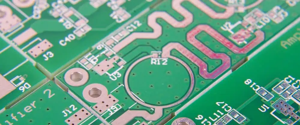
Fabric circuit board refers to the Printed Circuit Board (PCB) manufactured out of fiberglass. As one of the common materials, it allows for the flexibility and improved thermal conductivity of the circuit board.

In this article, we explain the concept of making fabric PCB, compare it to the other PCB materials and highlight some of the advantages.

What is a Glass PCB Board?

It refers to the circuit board manufactured using the fiberglass material. The use of this material is for a wide range of purposes, such as satisfying the industry standards, fitting the pricing requirements for PCBs and providing improved properties.

The Fabric Fabrication Process in Circuit Board

The fiberglass goes through some processes before it is readied for use in a PCB. Here are some of the things that go into the production:

Glass Interlacing

The first process is to weave (interlace) fibers of glass yarn, which are available in different thicknesses and densities. Note also that the weaving is done until the glass yarn takes the form of a โ€œfabric-like (fiberglass) sheet.โ€

Impregnation

The next step is to impregnate the fiberglass with epoxy resin. This is done for two purposes. The first is to form the cured resin (core) and the uncured resin (material) for the PCB.

Top Considerations for the Glass Fabric PCB

shengyi-s1000h-material-pcb

Certain measures need to be in place, if you are to get value from your fabric circuit board. The following are some of the top considerations when weaving or interlacing the fibers of glass yarn together:

1. The Tight Considerations

How tight the fabric is should make the list. Ideally, there are two options here: loosely-weaved and tightly-weaved. The rule of thumb is that the tighter the fabric is, the more uniform the dielectric constant becomes.

Here are some of the details:

Loosely-Weaved Epoxy Fill

If the epoxy resin is loosely-weaved, it tends to trigger a lot of issues in the circuit boardโ€™s laminate. These issues range from inconsistencies in the dielectric constant, fluctuations in the impedance and signal propagation skew.

Tightly-Weaved Epoxy Fill

On the other hand, the tighter the weaveโ€™s netting, the higher the chances of obtaining a uniform dielectric constant.

2. Zig-Zag Trace Routing

There is a risk of deriving an adverse impact of the weave glass style, when the traceโ€™s direction is routed across a weave of sparse weave glass style.

A better way to modify this is to use a โ€œzig-zag trace routingโ€ format. This provides for the angular routing of the trace relative to the strands of the fiberglass.

However, this is not entirely a remedy as it causes another issue โ€“ taking up more spaces on the PCB. When more board areas are taken up, the outcome would be triggering feasibility issues.

In light of this, it is best to use a medium-woven glass style, such as the 2116 glass style. This is a tightly-woven fiberglass material that helps to address the impedance issues for the high-speed trace layers.

3. Cost-Effective Compromises

While the tightly-woven material helps to reduce impedance issues; it also causes another issue. This type of fiberglass material is quite expensive.

To this end, it makes sense to go for a cost-effective variant, such as the 1080 and 106 glass styles. They provide for the optimization of the high-speed trace layers and lower-speed signal layers.

4. Use Spread-Glass Materials

You may also want to use the spread-glass materials, which aid the avoidance of inconsistencies in dielectric constants, especially for the ultra-high-speed transceiver signal board designs.

The Circuit Board Pattern Fabric Manufacturing Process

FULL PCB MANUFACTURING Quote

Your fabric PCB can be produced in real-time, if you follow the steps below:

1. Design the PCB

The first step is to use a Computer-Aided-Design (CAD) software to make the boardโ€™s design. Once this is completed, you have to convert it from a design to a PCB layout.

2. Prepare the Substrate

The substrate is prepared via the cutting and drilling of the boardโ€™s panel to the desired size and shape.

3. Layer the PCB

The layering process entails using a lamination procedure to add a layer of copper both to the top and bottom of the boardโ€™s substrate.

4. Drilling and Plating

The drilling of the board paves the way for the plating process. The drilling procedure requires the creation of holes for the PCB components. These holes will also be used as a medium of interconnecting the layers.

Once that process is complete, the plating process takes over. Copper is used to plait or cover the holes. This is a medium for creating the space for integrating the Thru-Hole (THT) components. The plaiting of the holes also helps to create the needed electrical connections between the PCB layers.

5. Solder Mask Application

A layer of solder mask is applied to the circuit boardโ€™s surface. The application serves two purposes:

  • It creates openings for the components to be placed.
  • Solder mask also helps to protect important PCB components, including the copper traces.

6. Silkscreen Printing

This is a method of highlighting, revealing or pinpointing the location of the parts on the PCB. Applying a silkscreen reveals the positions of the testing points, reference indicators, the PCB components and other relevant markings.

7. Testing the Board

The fabric PCB can now be subjected to a series of tests to validate the performance of the components.

What Forms of Fiberglass Exist?

Fiberglass, being the central material used for making fabric PCBs, has different forms. These forms include:

Fiberglass Cloth

This is the most relevant form of fiberglass. It includes glass fiber yarns. Despite the wide range of options, you can rely on the fiberglass clothโ€™s insulation capabilities.

Fiberglass Tape

This form of fiberglass comprises of glass fiber strands and is reputed for the excellent thermal insulation properties.

Fiberglass Rope

This form of fiberglass is best suited for the applications used for packing purposes. The fiberglass rope form is made of a braided yarn that is also composed of glass fibers.

The Different Types of Fiberglass

You can find the fiberglass grouped into different classes. Of course, these classes refer to the different properties of the fiberglass, as well as the typical applications or use cases.

Haven said that, here are some of the common types of fiberglass you can find out there:

A Glass

The components are 25% alkali and 72% silica. Commonly used for the window glass applications, the A Glass type is not entirely heat-resistant.

C Glass

The main components are sodium borosilicate and boron oxide. The properties include corrosion resistance and durability.

D Glass

Here is one of the most popular choices for Printed Circuit Board (PCB) designs. Featuring borosilicate-based fiberglass, the D Glass features improved electrical properties, low density and an impressive dielectric strength.

E Glass

This is the best option for the high-electrical-resistant applications. The E Glass is popular for the higher resistance to electrical current.

The major component is alumina-calcium borosilicate. Due to this, the E Glass is designated โ€œGlass-Reinforced Plastic (GRP)โ€ due to the ability to perform multiple tasks.

ECR Glass

Calcium alumino silicateย is the major component here. The outstanding property is the excellent corrosion resistance. This comes in handy for the prevention of the material from corrosion agents.

Fabric Circuit Board Applications

Rogers RO4835 PCB

Printed Circuit Boards (PCBs) made out of fiberglass tend to be used in a wide range of industries. The following are some of the supported use cases:

Automotive

The automobile industry benefits the most from fiberglass PCBs. These boards play a central role in the production of different components, which are, in turn, used with a wide range of automotive-related applications.

Consumer Electronics

Electronic devices used in the mainstream also benefit from the use of fiberglass for the design. The excellent electrical properties and outstanding mechanical capabilities make it ideal for use with specific consumer electronics, such as radios, computers and telephones.

Medical Devices

Medical devices and wearables are also configured with the fiberglass circuit boards. The dimensional stability and low-heat conductive capabilities are some of the reasons for the usage in this industry.

Aerospace and Defense

The aviation industry, military and paramilitary parastatals also benefit from the awesomeness of fabric PCBs. Of particular mention is the circuitโ€™s Glass Reinforced Plastic (GRP), which makes it a great fit for specific aircraft applications, such as instrument boxes and storage bins.

Fabric Circuit Board vs. FR-4

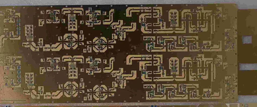
The fiberglass material is a popular substrate for manufacturing different kinds of circuit boards, such as multilayer PCBs, rigid circuit boards, single-sided boards, high-frequency PCBs and double-sided circuit boards.

On the other hand, FR-4 is a glass-reinforced epoxy laminate sheet, based on the fiberglass material. Although it is often interchanged for fiberglass, it is quite different from it.

Here are some of the clear differences between the two:

1. Cost-Effectiveness

If you are working on a budget, using the FR-4 material is not an ideal option. Rather, go for the fiberglass substrate, which is more affordable than the former.

2. The Components

Although both fiberglass and FR-4 circuits are made from a resin binder and fiberglass fabric, the FR-4 has more properties. One of its outstanding properties is the use of a woven glass fabric, as compared to the fiberglassโ€™ use of non-woven fiberglass fabric.

3. The Mainstream Usage

When it comes to the most-used fabric, the FR-4 material carries the show. Due to the reduced need for specialized manufacturing, the flame resistance and mainstream availability, the FR-4 substrate is now used across different consumer electronic products.

4. The Electrical Properties

Despite the fact that both the fiberglass and FR-4 materials have excellent electrical properties; the former has more to offer. In this regard, we consider its low dielectric constant โ€“ a property that makes it ideal for use with the high-frequency applications.

The Thermal Properties

This refers to the materialsโ€™ capability to withstand overt exposure to heat. It is better to go with the FR-4 materials, due to the fiberglassโ€™ slightly higher thermal expansion coefficient. This is the reason why the material is susceptible to warping.

The Benefits of Working with a Circuit Board Design Fabric

PTFE teflon pcb

Using a fabric-based material, such as fiberglass, for your PCB design, comes with a lot of benefits.

Here are some of the motivating factors for this decision:

Chemical Resistance

Fiberglass possesses top-notch chemical resistance, thanks to the capability of wading off the negative effects of chemicals.

However, you want to note that the material might be exposed to powerful alkaline compounds.

Impressive Strength

The impressive strength-to-weight ratio is also another upside. In this case, the substrate is best for the applications that require improved strength levels.

Dimensional Stability

Get you a PCB material that doesnโ€™t contour inappropriately. That is one of the outstanding features of fiberglass. Irrespective of the type of temperature it is exposed to, it doesnโ€™t contract, expand or change form in response to such temperatures and environments.

Electrical Properties

Applications requiring higher electrical insulation often use the fiberglass PCB material due to the exceptional strength and low dielectric constant.

Moisture Resistance

What happens when a PCB is exposed to (excessive) moisture environments? Often times, the moisture gets into the board and causes internal damages.

The exceptional moisture-resistance makes the fiberglass material a good fit for the applications that donโ€™t need overt exposure to moisture. This is also the reason why you can use the material across different environments, such as damp environments.

Fire Resistance

How susceptible is the substrate to catching fire? Despite the fact that the FR-4 material has been designated for such applications; the fiberglass substrate also stands a chance. Here are some of the things to know about the fire resistance capabilities:

  • The material has a higher degree of strength retention. This is put at the retention of up to 25% of the strength, irrespective of the exposure to up to 540-degree Celsius of temperatures.
  • Fiberglass materials neither propagate fires nor burn when exposed to one of such.
  • There is a higher chance that the material doesnโ€™t bring forth smoke. This is largely attributed to the inorganic material content that doesnโ€™t make a spontaneous ignition of flames, especially when subjected to heat.

Conclusion

Fabric circuit boards do not catch fire, ignite the same and they have excellent electrical and thermal properties. Contact us today to start discussions on how to optimize your circuit board design and fabrication.

A Comprehensive Guide to Chip Scale Package – CSP

Chip Scale Package

CSP means you are using just one chip for this purpose. The size of the chip you are using in this process matters a lot. It is easier to determine it with the surface-mounted ICP standard to avoid any complications. 

Bear in mind when we are talking about CP, we mean quality and efficient performance. All the chip-size BGAs are crucial for minimizing the area. Now if you are thinking CSP relates to production and construction, then you need to rethink. There are fewer but highly important applications in different domains in terms of using CSP. 

It is because these packages need precision, and only a few manufacturers can meet your expectations in this regard. On that note, there are different versions of CSP packages that are common today. So what exactly chip size packages are important for? You mainly use them in portable and small electronics. 

It’s time to learn about the structure and the working of a standard CSP bundle. For this, we have discussed it in the following pointers for you!

Structure & working of a Chip Scale Packaging bundle:

CSP
CSP
  • The interposer of the chip size bundle is not open; instead, you use it in a covered form
  • Epoxy resins are reliable to use for CSP before the method starts
  • Since epoxy is nonconductive, its main role is to join the wires with the circuitry when you place the epoxy under your setup
  • The shapes of the epoxy are important as they help in minimizing the size of your CSP bundle when they are near the die
  • Once you have completed the procedure, its time to size the solder balls present beneath the interposer as well

Features Of Chip Scale Packaging 

Every great thing has salient features that make it stand out from the crowd. Owing to these features, you are now able to use your favorite portable devices on the move. So in this section, we are going to have a look at the unbelievable benefits of CSP that make this technology the way it is as well.

Benefits of Chip Scale Packaging:

  • One major benefit is that CSP supports small package sizes, which you always need to produce portable devices
  • CSP is also useful in solidifying the interconnections 
  • It greatly minimizes the size of the setup
  • Once you are successful in reducing the size, it will eventually lower the weight and cost production of your setups as well
  • CSP is a viable tech for assisting you with the easy and quick assembly of packages
  • It also does not need self-alignment, which helps producers with controlling their production budget
  • There is an impressive margin of teaming up CSP with SMT that will enhance the ease of production of packages in bulk
  • The SMT combined with CSP will enable producers to rely on multiple types of dies in case of emergency
  • The interposer will also contribute to minimizing the size by not compromising the CSP at all due to using SMT for this purpose

Common Forms of Chip Scale Package

Today, different versions of CSP are common in the market. These are:

  • BGA
  • Leaded
  • Non-flip chip
  • Wire bonded
  • Flip chip

We are briefly taking a look at all these types in this last section; letโ€™s get started with it!

1. Flip Chip

Flip-chip is useful when you need to play with the CSP from different directions. Also, flip chips come in handy when there is a need to join the CSP with the workpiece substrates. Standard CSP uses copper pillars and solder for forming the connections. The pads entirely cover the surface, which helps in reducing the size of the package on the whole. There is no need to use any sort of adhesives, and due to this reason, you can lower the signal inductance to a large extent.ย 

2. Non-Flip Chip

FULL PCB MANUFACTURING Quote

Non-FC is an old type of CSP that still has important use cases for us to study. There are electrodes that you need to rely on when using non-flip chips. These are mostly present on the upper surface of the SMC covering. You can also find these non-flip chips on the light radiation layer and P-type SMC layer as well. Wait, what exactly does this P layer do in this whole process? The role of the P layer is to make the thermal sink happen around the sapphire material. If the sapphire fails to produce adequate heat conductivity, it will hamper the system for the same purpose as well. It means totally disrupting the efficiency of the chips. The electrodes that we just talked about are positive, and sometimes these can be the culprit for weakening the non-flip chips in the worst-case scenario. Also, using these electrodes needs precautions. If they are too close to each other, this can even cause short circuits as well.

3. Wire Bonded 

Wire bonding means you are using wires to connect the chips and semiconductors for efficient performance. So how exactly wire bonding relates to this efficiency on the whole? So the wires you are using for wire bonding are extremely thin and made of conductive metals like gold and aluminum. Wire bonding is not only helpful in connecting chips with semiconductors. But also aids in merging PCBs with their dedicated electronic devices. It is an affordable method and also easy to perform. 

4. Ball Grid Array 

BGA is useful for SMT packaging of complex and compound circuits. For instance, microprocessors use BGA for efficient performance in the long run. BGA is more reliable than dual packs since it offers more features. The bottom portion of the setup only supports the perimeter and is inactive for the rest of the components. You can also use the imprint for regulating the perimeter for the sake of improved performance. 

5. Leaded 

COL involves mounting the crystals and dies on the frames instead of regular pads. If you are mounting crystals on the frames, it will surely offer more benefits as well. So what it should be? Leaded CSP does not need wire bonding at all, unlike others. Impressive, isnโ€™t it?

Top 12 Hex Inverter ICs – All you should know

Hex Inverter IC

Hex Inverter is a type of Integrated circuit. The Hex in the name represents Hexa which means six. It comes with various benefits and features. These ICs are mainly used as amplifiers for analog converters among the logic series, shift levels, and added delay.  

However, you may still be concerned about why they act as an essential component in many devices and how it functions. This article gives you a detailed insight into the features, functionality, working principles, application, and types of Hex Inverter Integrated Circuits. 

Functions of Hex Inverter

Letโ€™s look into some types of hex drivers along with their functions and roles. Hex IC-4069 contains hex means six in total circuits. This type of CMOS hex IC inverter can be used in applications, especially which does not require features of medium power source TTL drives and logic-level converters.

Hex IC-7414 contains inputs of LSSTL or Schmitt trigger. Eventually, the input of Schmitt triggers converts the slow-paced signals into efficient output signals. 

The IC-7407 acts as a hex buffer that contains collector outputs. This hex buffer consists of three-phase internal circuits which create noise immunity and stable output. 

The IC-7405 consists of an open collector and output of high voltage. This simply means that it gives output with a higher voltage.

The IC-7404 also acts as a buffer. It contains a 14-dip variation integrated circuit. This makes it capable of performing six inverter insertion actions.

Applications Of Hex Inverter ICs

Hex Inverter
Hex Inverter

ยท Digital Logic Gates

Hex inverter integrated circuits serve as foundation components in digital logic gates. As it takes the input values and gives back the output value. This implies that if the input is of high logic, it returns the value of output in low logic. However, if you connect various hex inverter integrated circuits together, it generates even more complex and hard logic gates which include XOR, NOR, and NAND gates.

ยท Oscillators

Hex inverter integrated circuits are also utilized in oscillators. It helps in generating square waves, sine waves, and clock signals. The circuit of the oscillator contains a feedback loop. This loop includes a capacitor and a resistor. The capacitor starts charging and discharging over the power supply over the determined rate by the capacitor and resistor values. However, this creates a frequency waveform that serves as a sine wave or clock signal.

ยท Data Transmission

Hex inverter integrated circuits can also be utilized in circuits of data transmission which convert the digital signals from one level of voltage to the other. For instance, in serial communication of RS-232, the range of voltage of transmitted signals can vary between -12 volts to +12 volts. Therefore, many computers and microcontrollers use 5 volts and 0 volts logic levels. The hex inverter integrated circuits make it possible to convert those RS-232 level signals to levels of TTL.

ยท Signal Conditioning

The hex inverter Integrated can also feature in signal conditioning PCBs to convert the signals from analog to digital form. For instance, the hex inverter integrated circuit, along with the comparator, helps in converting the analog signal form to a digital form. The comparator gives an output value that goes into a hex inverter integrated circuit. There, it inverts the form of signals and creates a digital signal output.

ยท Power Management

The Hex inverter Integrated Circuits are also used in the management of the circuitโ€™s power, which controls the voltage supply to all other electronic components. For instance, hex inverter integrated circuits make it possible to set up the output voltage level. Moreover, it also helps in generating feedback signals. These signals further help in adjusting the output voltage of the regulator.

Hex Inverter IC 74HCT04

The IC-74HCT04 inverter consists of six self-maintaining inverters with pull and push outputs. Its pins have lower-power Schottky which enhances the speed of the IC. Moreover, it also owns a special protection network of diodes that protects the input pins from higher input Vcc. The diodes simply activate the current limiting resistors, which automatically protect the input pins.

Features of Hex Inverter Ics

The IC-74HCT04 offers various features. It is lead-free and ROHS compliant and found in packages like TSSOP-14 and SO-14. Moreover, it possesses a voltage range of 5.5 volts to 4.5 volts, along with a constant current output value of +25mA. It offers 2 volts of max value of higher input voltage and 0.8 volts of minimum value of low input voltage. Along with this, it has a 29 ns propagation delay and offers input of Schmitt trigger.

How To Use 74HCT04?

As this IC has NOT gates, t shows that it has specific output and input terminal or pins. Therefore, make sure to connect pin 16 of the IC to the power source. Then connect pin 8 with the ground. And it starts working.

ยท Propagation Delay of 74HCT04 Inverter Circuit 

The IC-74HCT04 acts in the form of a wave buffer or oscillator. However, this may require some factors to consider, like propagation delay or switching time. It refers to the period in which an output pin switches the type of input signals into another form. The propagation delay of this module is 29ns. This makes it ideal for several devices, which include buffering generators, clock signal generators, and a generator of square waves.

Hex Inverter IC 4049 IC

The Hex inverter 4049 Integrated circuit also acts as an inverter buffer with six or hex NOT gates. It is widely used in the Converter of CMOS TTL. Moreover, it is also used in various devices that have DTL converters. Additionally, it does not only function in TTL but also in DTL.

Features of Hex Inverter IC 4049 IC

The IC-4049 uses a voltage multiplier PCB and creates the max input value of the voltage supply. Moreover, it acts as a logic function of a Hex inverter buffer. It possesses various packages, which include PDIP, SO, TSSOP, and SOIC. Additionally, the max sink current of the module can rise to 2 TTL loads. It also provides a 22.5pf maximum value of input capacitance, 50mA max supply current, and an equilibrium temperature range of -40 to +85 degree Celsius.

How To Use Hex Inverter IC 4049 IC?

FULL PCB MANUFACTURING Quote

IC-4049 serves as a central component in the double voltage circuit of 12-24 volts. Moreover, IC-4049 works in a similar way as a rectifier circuit. Nevertheless, a double voltage circuit does not only convert Direct Current to Alternating current but also configures the voltage of Direct Current. Therefore, these circuits become useful for devices that are concerned with high Direct current voltages.

Applications of Hex Inverter IC 4049 IC

IC-4049 is used in various types of applications and devices. Some of them include O/P reversing, Source drivers, CMOS hex converter, voltage multiplier PCB, and CMOS converter to TTL or DTL.

Hex Inverter IC CD4069

CD4069 hex inverter Integrated Circuit works in a similar way as IC-74HCT04. This enables both integrated circuits to enable noise immunity.

Applications of Hex Inverter IC CD4069

CD4069 hex inverter Integrated Circuit offers various types of applications and uses cases. It is used for pulse framing and logic reversal. Moreover, it is also used to make amplifiers with higher input impedance and oscillators.

Top 12 Hex Inverters

1. 74HC04

The CMOS-based 74HC04 hex inverter Integrated circuit works within the voltage limit of 6 volts to 2 volts. However, it does offer various features like higher capability of output drive, low consumption of power, and higher noise immunity. All these features make IC-74HC04 ideal for various digital electronic devices. Moreover, IC-74HC04 has a value of 10 ns propagation delay and a 5.2 mA max value of output current.

2. CD4049

The CMOS-based IC CD4049 hex inverter Integrated Circuit works within the range of voltage of 18 volts to 3 volts. This IC offers features like higher capability of current drive, lower consumption of power, and higher input impedance. Because of these features, this IC is used in various electronic devices. Moreover, IC-CD4049 has a value of 25ns propagation delay and a six mA max value of output current.

3. SN74LS04

The TTL-based IC SN74LS04 hex inverter IC works within the voltage limit of 5.35 volts to 4.75 Volts. It offers features like a higher capability of output drive, lower consumption of power, and high speed. These features enable this hex inverter IC to be used in almost all digital electronic grades. Moreover, this IC has a 15 ns propagation delay and an 8mA max value of output current.

4. 74HC14

The CMOS-based 74HC14 hex inverter IC operates over a voltage of 6 volts and 2 volts. It offers features like the input of Schmitt trigger, low consumption of power, and higher noise immunity. All these features make this hex inverter IC ideal for digital consumer devices. Moreover, it also has a value of 14 ns propagation delay and 5.2 mA max value of output current.

5. CD4069

The CMOS-based CD4069 hex inverter Integrated Circuits operate between the voltage of 18 Volts and 3 Volts. Additionally, it offers features like higher capability of current drive, low consumption of power, and higher input impedance. This makes it ideal for use in digital consumer electronic devices. Moreover, it has a max value of current output, six mA, along with a 35 ns propagation delay.

6. SN74HC04

The CMOS-based SN74HC04 hex inverter Integrated Circuits operate within the voltage of 6 volts and 2 volts. However, it offers features like a high capability of output drive, low consumption of power, along with greater noise immunity. These features enable this IC inverter best for digital consumer devices. Moreover, it also has a ten ns propagation delay and a 5.2 mA max capacity of output current.

7. 74LS04

The TTL-based 74LS04 hex inverter Integrated Circuit operates within a voltage of 5.25 Volts and 4.75 Volts. It offers features like low consumption of power, greater capability of output drive, and high speed. Thus making it ideal for digital electronic devices. Moreover, it possesses a 15 ns propagation delay and an eight mA max value of output current.

8. CD74HC04

The CMOS-based CD74HC04 hex inverter Integrated Circuit functions between the voltage value of 6 Volts and 2 Volts. The features like high capability of drive, low consumption of power, and greater noise immunity make this hex Inverter IC to use in various digital consumer electronic devices. The IC-CD74HC04 contains a 10ns propagation delay and 5.2 mA max output ampere.ย 

9. MC14069

The CMOS-based MC14-69 hex Inverter Integrated Circuits work between the voltage level of 18 volts and 3 volts. Features like the high capability of output drive current, low consumption of power, and high impedance input make it ideal to use in digital electronic devices. Moreover, the IC-MC14069 contains a 35ns propagation delay and max current output of 6 mA.

10. 74HC240

The CMOS-based 74HC240 Hex Inverter Integrated circuit works between the voltage level of 6 volts and 2 volts. It serves as a line driver or a buffer in several digital electronic devices. The IC-74HC240 contains the max current output of 35mA along with an 8ns propagation delay.

11. CD74LS04

The TTL-based CD74LS04 hex inverter Integrated Circuit works between the voltage level of 5.25 volts and 4.75 volts. Its low consumption of power, high capability of output drive, and high speed make it perfect to use in various digital electronic devices. Moreover, IC-CD74LS04 bears the max current output of 8mA along with a 15ns propagation delay.

12. 74ACT04

The CMO-based 74ACT04 hex inverter Integrated circuit operates between the voltage level of 5.5 Volts to 4.5 Volts. It offers features like low consumption of power, low impedance of output, and high speed, which makes this IC ideal for various digital electronic devices. Moreover, IC-74ACT04 bears a max output amperes of 24mA along with a 6ns propagation delay.

Conclusion 

An appropriate and suitable Hex Inverter Integrated Circuit determines the efficient and reliable operation of your device and application. Therefore, make sure to choose the appropriate Hex IC Inverter.

The above-mentioned twelve Hex Inverter Integrated Circuits are widely used in various devices and applications because of their advanced specifications and features. Moreover, make sure to take into account a few factors while choosing the right Hex IC inverter. These factors include propagation delay, output current, power consumption, and voltage power.

What is Moisture Sensor Circuit? Construction, Working & Advantages

moisture sensor circuit

The soil moisture or moisture sensor mainly refers to a type of device that senses the moisture percentage in the soil. It is widely used in the frame, agriculture, and field projects. Other than farmers or engineers, hobbyists also use them in a wide range. 

The moisture sensor contains two main parts. One refers to the main circuit or board, while the other refers to the sensor plate. It contains probes half-buried in the soil which makes them vulnerable to rusting. Therefore, they need extra caution and care to work. For this, you can also use another customized probe that has better durability. 

Moreover, moisture sensors give output in two types; digital form and analog form. However, the type of output solely depends on the user and how they want their output values. Furthermore, the longer use of these sensors creates a layer of salt over the probes. Therefore, keep them clean and moisture free now and then.

Construction of a Moisture Sensor Circuit

Moisture sensors can have different types of schematics depending upon the type of sensor. However, this simple schematic diagram of the moisture sensor of soil contains various types of basic electronic components. It includes an LM393 Integrated circuit, a double voltage comparator that can be seen in other types of sensors too. It is considered the sensorโ€™s heart, along with half-buried probes in the ground. Furthermore, it contains an onboarding status led and a potentiometer incorporated over the PCB. Both support moisture soil sensors to detect and find the moisture present in the soil. Besides this, it also helps the sensor maintain microcontroller values.

Make sure to keep soil and PCB away from each other so that they wonโ€™t cause any type of error in the values of the sensor. Also, this protects the probe’s pin header from corrosion while exposing it to moisture. Moreover, this sensor contains a high voltage range which makes it ideal to use with any type of microcontroller. But it gives altered values as per the type of microcontroller.

Working on a Moisture Sensor Circuit

A soil moisture detector follows a similar working principle as the LM393 IC sensor. However, they only differ in terms of the outputs they produce. Probes play an important role in detecting soil moisture. They are buried half in a field or ground and sense the amount of moisture present in the soil. However, if we see at the facts, the probe does not sense moisture. It measures the level of voltage, which refers to the analog sensor value that a microcontroller gives out. The probe is linked with the ground from one side and with a first comparator non-inverting input from the other side. Senor contains one capacitor of 0.1ยตF and one pull-up resistor parallel to the probe. In the last, the comparator comes in and decides the value of the output.

Fertilizers, pesticides, or any type of insecticides can alter the actual value of a moisture sensor. Therefore, use some kind of algorithm or PID to get the correct value of the moisture.

Advantages of Moisture Sensor Circuit

This type of moisture sensor comes with great features and advantages. It comes at affordable prices and is available easily in the market. Therefore, you wonโ€™t find a shortage of these sensors. It provides outputs in both types, including potentiometer and onboarding status led to adjust the values. Moreover, the PCB quality seems much better than the probes. Furthermore, this sensor can mount on any type of PCB surface because the circuit board uses a mid-hole to screw the PCB over any type of surface.

Disadvantages of Moisture Sensor Circuit

Regardless of its amazing benefits and features, soil moisture circuit sensor also comes with drawbacks. The biggest drawback is the Probesโ€™ PCB quality. Many engineers and users do not seem to like the quality of these probes much. Because due to the moisture, probes start covered with a salt layer. Moreover, moisture also causes corrosion in the headers of pins and the connected wires, as they need checking now and then.

Applications of Moisture Sensor Circuit

Because of its easy usage, amazing features, and benefits, it’s widely used in various types of projects. Many engineers and agricultures tend to use this sensor and get better results.

FAQ about Moisture Sensor Circuit

What Is The Voltage Level Of The Moisture Sensor Circuit?

The LM393 Integrated circuit datasheet shows that it operates on a voltage of 36 volts. Therefore, it’s safe to connect the sensor to any level of voltage despite any logic level of voltage.

How To Dodge or Prevent the Depositing Coatings Of Salt Over The Moisture Sensor Circuit Probes?

FULL PCB MANUFACTURING Quote

The usage of commonly available probes or even copper probes can help in measuring the moisture value in soil. Thus, it gives better durability.

Can I use the wire with Long connections Between Main Board & Probes?

You may increase the length of the wires that connect probes and the mainboard. However, it may increase the wire’s resistance more than the conventional jumper wires. Thus resulting in altering the values.

Is there any effect of Fertilizers on the values Of Moisture Sensor circuits?

Yes, pesticides and fertilizers can have an impact on the values because they enhance the free ions content present in the soil. Thus, resulting in improved voltage signal conduction. Therefore, those extra free ions act as moisture and alter the values of soil moisture.

Understand the Thermocouple Circuit Working Principle and Its Applications

The thermocouple refers to a temperature-measuring device. It is used in various types of devices and applications. It transforms the change of temperature in an electrical voltage. However, the thermocouple operates over the thermoelectric effect working principle. This article explains the diagram, circuit, advantages, disadvantages, and application of thermocouples.

A thermocouple also refers to an Active Transducer. A thermocouple does not need any outer power supply to operate or work. It generates a voltage on its own, regarding the fact that it has a small magnitude. However, thermocouple cost less, construct easily, and have the ability to measure large amounts of temperature.

Moreover, a thermocouple contains two wires of metal that join with each and make a junction point. When that specific junction feels any type of temperature change, it creates voltage. Typically, thermocouples are specially designed to measure or sense the difference in temperature as compared to the normal temperature of the environment. This implies that it uses the temperature of the environment as a reference temperature. However, thermocouples use two junctions in which one has a cold temperature.ย 

Principle Of Thermocouple Circuit 

Thermocouple Circuit diagram

A thermocouple working principle follows three distinct types of effects.

ยท Seebeck Effect

This type of effect happens between two distinct metals. However, when one metal goes through heat, it starts flowing the electron from the heated metal to a cold metal. This induces the direct current in a circuit.

In simple words, the Seebeck effect refers to a process in which the difference in temperature between two distinct metals induces the difference potential between them. This effect creates a small amount of voltage per kelvin temperature.

ยท Peltier Effect

The Peltier effect simply refers to an inverse effect of the Seebeck effect. It represents that one can easily create a temperature difference between two distinct conductors by just providing a potential difference between both conductors.ย 

ยท Thompson Effect

Thompson’s effect represents that whenever two distinct metals join with each and create two junctions, then due to the Tg or temperature gradient, the voltage may induce the entire conductorโ€™s length. The Tg or temperature gradient refers to a physical term. It represents the direction along with the rate of temperature change over a specific location.

Construction Of Thermocouple Circuit 

The thermocouple contains two distinct metals. Both metals weld together at a point of junction. However, this junction serves as a measuring point. These junction points have three categories.

ยท Ungrounded Junction

This type of ungrounded junction contains conductors totally isolated from a protective sheath. However, it is mainly used in applications that work under pressure. Moreover, its main goal is to reduce the stray magnetic field effect.

ยท Grounded Junction

These types of grounded junctions weld the protective sheath and metals together. Moreover, it helps in temperature measurement in corrosive areas. Furthermore, it provides noise resistance.

ยท Exposed Junction

These types of exposed junctions are only used in specific places where one requires a fast response. Moreover, exposed junctions also help in measuring the gas temperature.

Also, the selection of thermocouple material depends on the temperature measuring range. 

Measurement Of Thermocouple Circuit Output

One can easily measure the thermocouple EMF output through various methods. Some of them include:

ยท Multimeter

Using a multimeter proves to be one of the simplest methods to measure the thermocouple output EMF. The thermocouple connects the multimeter with its cold junction. Moreover, a multimeter pointer deflection falls equal to the amount of current flowing through it.

ยท Potentiometer

A DC potentiometer can also help the thermocouple to measure the output.

ยท Amplifier

Thermocouple uses an amplifier to amplify the output. Then it sends the amplified output to an indicating or recording instrument.

Advantages Of Thermocouple Circuitย 

FULL PCB MANUFACTURING Quote

Thermocouples give various benefits; therefore, they are used in almost all transformers. The transformer contains a hot junction, while the externally mounted meter contains a cold junction.

This simple installation of a meter and transformer helps the meter to read the rise of temperature in the oil compared to the surrounding location. Moreover, due to their low cost and rugged installation, a turbine hall can use thermocouples around them exclusively. Also, a thermocouple can measure a great range of temperatures as compared to an RTD.

Disadvantages Of Thermocouple Circuit 

Apart from giving benefits, it does have some disadvantages too. Thermocouple requires expensive extension-level compensating cables or thermocouple wire if it is present at a distance from a measuring device. Moreover, thermocouple does not work in regions of high radiation, such as reactor vaults. Also, radioactive radiation can add voltage inside thermocouple cables.

As the thermocouple releases a signal in the form of voltage, any additional voltage can cause an error in the output of the temperature transmitter. Furthermore, it gives a slow response as compared to RTDs. If it has remote control logic along with a temperature transmitter, then it may cause power failure. Thus resulting in faulty readings.

Failure Modes of Thermocouple Circuit 

Thermocouple also has failure modes. If the thermocouple device has an opening circuit, then it does not allow the current flow. This results in off-scale or low readings of temperature. Moreover, other than open circuits, short circuits also cause off-scale readings of temperature. A short circuit allows the leakage of current to GND and small voltage.

Applications of Thermocouple Circuit 

Thermocouples use in a variety of devices and applications. It has a vast range of industrial use like iron and steel industries. They use thermocouples to measure the temperature of production. Moreover, it uses in HVAC systems.

It helps in monitoring the room temperature, ambient temperature, etc. it also uses in devices of temperature control. These devices include refrigerators, air conditioners, and heat pumps. Here, thermocouples control the temperature system automatically. 

What is the Significance of Electronics BOM?

HOW TO MAKE BOM

When bakers are baking, they need to get the necessary ingredients to bake bread or cake. They need ingredients like sugar, butter, and flour. Furthermore, they need to gain access to important tools such as mixers, pans, bowls, amongst others. This baker must ensure there is a list that comprises everything needed for baking before heading to a store to buy the supplies. They can remember everything to buy and how much of each item to buy thanks to this list.

Now let’s imagine this list was created by the client rather than the baker. Things may get worse if the baker rarely spoke to the client face-to-face. Therefore, the list of items to buy was the means by which the consumer disclosed what was necessary.

Additionally, this list includes necessary details for each item. This list is similar to. Bill of Material, popularly known as BoM.  The distinction is that you need to create a hardware like PCB, as opposed to baking a cake.

What Does a BOM In Electronics Mean?

What the bill of material means will be covered here? The BOM can be is simply a thorough list of the sub-assemblies, bom electronic components, and  raw materials for manufacturing a circuit board. Also, it includes assemblies that are needed for the manufacturing of the product. Additionally, the information in their manufacturing BOM helps manufacturers to develop or construct a particular item. Therefore, there is a great need for accuracy, precision, and good documentation.

Furthermore, if customers order circuit boards, they make use of  BOMs to describe their needs to the PCB assembler. Then this PCB assembler integrates the BoM when creating the circuit boards to function according to the demands of the customer.

BOMs are crucial to Rayming PCB’s assembly services. They collaborate with PCB producers and assemblers in a similar way.

What You Should Know Before Making an Electronics BOM?

bom bill of material

You need answers to these questions before you build or cretae your BOM.

What are you going to construct?

You must have started the PCB designing phase before beginning the BOM stage. Failure to do this might cause misunderstanding when interpreting the BoM. Also, when creating the BoM, you could start gathering accurate information about the parts required.

However, until your printed circuit board design is complete, you cannot rapidly start designing the BOM. Additionally, confirm that the Gerber file is created and that the everything is going as planned. The circuit board manufacturer can better understand the design details with the help of the Gerber file. Additionally, this stage aids in identifying the bom electronic components that you require to include in the BOM.

Who may utilize it?

The document’s content makes it ideal for use in various departments during PCB fabrication, including purchasing, design, engineering, and manufacturing. Therefore, thinking about who is in need of the BOM will help you provide precise details.

What details ought to be provided?

At this point, you need to be able to comprehend the details and get familiar with them. Understanding the categories you want to have in your document is necessary, also.  All BOMs must have some basic information like amount, part name, as well as quantity. There are other optional details you can also include. It is important you decide the addition of consumables such as bolts and glue. However, you need to understand that creating a BOM that has the necessary details is the best decision you can ever make

What particular program would you employ to create it?

Before you create a BOM, you should ensure you know the program you’ll be using. The BOM list comprises  a spreadsheet, a good number of businesses integrate the Excel. You will also realize that you require an excellent tool that is specifically made for BOMs, of which there are many.

What Information Should Be in the BOM?

SMT Bom checking

The BOM’s entire details for the PCB assembly could vary based on the project. Here is a list of some information a BOM usually contains.

Description

This description offers information about each component within the BOM. This includes its dimensions, color, voltage, and others. The information helps you to be sure you are ordering  the best component and as well prevents any form of misunderstanding caused by similar pieces.

It is important your BOM includes all the appropriate measuring units. The choice of the items that comprise multiple units has to be constant all through the document.

The manufacturer’s name

You will need to include the name of the manufacturer of the component for enough precision. With this, it is much easier for those using the BOM to identify the best and most appropriate component to use. Additionally, it is a thoughtful decision to confirm with your manufacturer if each item on the list is available before you proceed to list it.

Additionally, make sure some factors are well considered. For instance,  cost, delivery time, and specifications must be enough for your project. In the long run, it will save excessive expenses and the effort needed to get a replacement item much later all through the process of manufacturing if details are quickly examined.

Quantity

The quantity of each component required is another important detail your BOM must include. Therefore, be certain that the data is accurate and very up-to-date. This will help you gain benefit more from the price breaks provided for purchasing items in large quantities.

Type of Procurement

Ensure that you get the proper part by simply listing your type of procurement on your spreadsheet. This information reveals how to create a specific component.

The flexibility metric

You could get a better production process if you clarify the flexibility required ย in your BOM. This required for grouping the goods based on your flexibility with them. Some parts can be classified as critical. Therefore, the assembler has to integrate the correct specifications in such a case.

Other parts might be crucial to the design, however you might be able to replace them with some identical components made by a different company. Other requirements must be followed by the maker. With Rayming PCB, they never substitute or change a product without first consulting the client.

Replacement Parts

BOM Creation for PCB Assembly Manufacturer

If the requested component isn’t available or there will be another modification, it is advisable to always include backup parts. You will be able to reduce the time you’ve wasted in each of these cases.

Level of BOM

BOMs usually feature various tiers. Each of these BOMs represent the sub-assembly or primary. In order to make navigation easier for and as well comprehend the assembly, each BOM features a distinct structure and product structure trees assigned and segmented based on their BOM levels.

Additional Files

In cases like this, you will have to generate files during the PCB production. These files include data sheets, CAD files, schematics, and instructions, which arenโ€™t suitable for the BOM spreadsheet. In such cases, you have to include any supporting papers, and make sure there is a connection to the proper BOM level and components.

Reference Designator

When making the distinctive reference designator of each component of the circuit board assembly, be sure to indicate where each component sits on the board. Making the designator consistent with the level utilized in the PCB design docs makes it simple to cross-reference the PCB layout as well as BOM. The identifiers typically consist of a letter and a number.

Package Design

Include the materials paperwork, the description of the package, etc. These packages’ design helps to streamline production, and selecting the best packaging type could guarantee that the procedure becomes more efficient and cost-effective.

Placement Technique: Ensure the technology and the placement technique used in your PCB projects are provided.

This describes how each component is linked to a printed circuit board. Surface mount and through-hole are the techniques.

Footprint/Points

Here, you need to define the connecting points possessed by every component on its circuit board. Furthermore, it is crucial to define the footprint of each part. This usually gives more insight on the physical attachment of the connector to the printed circuit boards and subsequent electrical connection, like pads in surface mount technology and through-holes. Also,  you need to pay attention when recording the footprint, points, BOM level, and separate component points.

Phase

Also, it might be necessary to add some blank space to the document. This will help you to mark the locations of the different lifecycle components.

Comments and Notations

Although this category might not be crucial, it could help in enhancing the productivity of your project, in cases when there are unforeseen issues or modifications. Any thoughts and comments that arenโ€™t suitable in any other categories should be here.

What are the BOM Creation Tips?

The Method of Creating Bill of Materials (BOM)

We have listed some tips that you can work with when designing your electronics BOM.

Tailor your electronic bill of materials to your requirements

You have to decide what businesses you’re partnering with need from your BOM and then adjust to the design in order to meet those needs. The fact is that different businesses handle BOMs in various ways. Moreover, distinct projects need different details,  organization, and feature. Also, you can customize your bom to work according to the specifications and needs of the project.

Use a template

It is possible to get BOM template form your manufacturer’s websites before obtaining a quote as well. When you make use of the template provided by the firm, you will be able to prevent problems that come with opening and reading a BOM document.

Ensure you provide important facts

Provide as much useful information as you can in your document. Keep in mind that such BOM is crucial in providing more information to those who must construct your Circuit board from scratch. It’s could be your first time of relating with these people and you need to know they don’t use precisely the same language. This is the reason why the BOM must be detailed, precise, as well as clear.

There are some particular details that aren’t useful  and they can be confusing. But always use your professional judgment.

Check your information.

Before any uploading of the electronic bill of materials, ensure you make a thorough check for every piece of information. Also, be certain that the data is accurate and precise. The smallest mistake might cost you a lot when it comes to PCB manufacturing.

Monitor your alterations

Make sure there is a system is in place to help you track the modifications in your document. You may occasionally desire a history of earlier iterations. This is for reference purposes only. Make sure each version is clarified while making emphasis on the most recent one utilized for the project.

Cut back on the editing options

Despite the fact that several entities have access to a BOM, never give them the rights to edit until it is completely required. As an alternative, you ought to provide them “read-only access”. When you donโ€™t give any rights for editing, you can minimize mistakes and unintentional modifications. For those with editing ability, you may also have to create a special ID.

Try to think about automating

You need to integrate a BOM management process might include automation-related elements. This will definitely make it easier to discover if there are any differences within the records. Furthermore, it helps to ensure improved traceability. Also, it is easier to export and import data for use in different formats.

Conclusion

The Bill of Material (BOM) is considered a thorough list that includes components, raw materials, sub-assemblies, including assemblies that are required for the manufacturing of a product. Before you begin with designing the BOM,  you must have started with the designing stage of the project. If you don’t begin with this stage, the BOM you created might not be comprehendible. Additionally, as you’re creating, you could as well get accurate information about the parts needed. However, until your printed circuit board design is complete, you cannot rapidly start constructing the BOM. Additionally, confirm that the Gerber file is created and that the plan functions as planned.

RayMing PCB & Assembly puts quality in mind while providing tons of circuit board services and completed products. They include procurement, assembly, as well as fabrication. Also, we provide other services like ordering, reordering, and quick online quotations.