What is a Load Cell Circuit? A Complete Guide

load cell circuit

FUTEK introduced load sensors or cells to the industry. The company has produced a wide range of load sensors of force transducers. These cells are produced with high-tech sensor technologies like strain gauge with metal foil technique. A

 load sensor also refers to a force transducer. It takes the input in mechanical weight, tension, pressure, or compressor. Then convert that into electrical signal output. Load cells come in various types of capacity, geometry, and size.

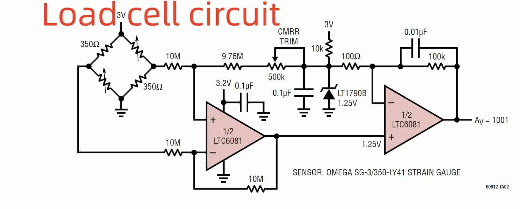
Strain Gauge Load Cell Circuit

Load cells refer to a type of force transducer. Generally, it takes the input in mechanical form, which includes pressure, compression, weight, tension, and load. However, it then converts that input into standardized, convertible, and measurable electrical signals output. When the applied force increases in the load cell, it proportionally changes the electrical output signals.

The load sensor became an integral part of various industries. These include automotive, robotics, pharmaceuticals, medical, industrial automation, defense and aerospace, and high-precision process manufacturing. All these industries have one thing in common. They all want high, reliable, and precise measurement values. Recently. Surgical robotics and Cobots join hands together and produce innovative measurement devices.

Working of a Load Cell Circuit

FULL PCB MANUFACTURING Quote

To understand the working principle of load cells, you must look into the physical details of the strain gauge. It also refers to strain gage load cells or simple strain gages. A strain gauge with metal foil refers to a type of sensor that changes its electrical resistance when force is applied. Simple, it converts the pressure, force, compression, weight, or any mechanical tension into a measurable electrical resistance.

Strain gauge acts as electrical conductors that are attached to a film in the form of a zigzag shape. However, when the film pulls the strain gauge, it elongates or stretches. However, it gets short or contracts over the pushing effect. Thus, this change in shape creates changing in electrical conductors’ resistance. However, this principle simply explains the force that is applied over these load cells. Simply, the resistance of the strain gauge increases when an external force is applied over it. Load sensors work in the same way.

Force or load sensors consist of a metallic body that contains a strain gauge foil attached to it. The body of the load sensor uses materials like stainless steel or aluminum as both materials provide load sensors, two features. It offers great sturdiness that helps it to withstand and bear heavy loads. It offers flexibility to the sensor, as it changes its shape when the force is applied while getting back to the original form as the force is removed.ย 

However, when a certain type of force or strain applies over the sensor metal body, it starts acting as a spring. It deforms from its original shape and returns to normal form as the load or force is removed. As the body deforms, it changes the strain gauge shape, too, while changing the electrical resistance eventually.

Thus creating a variation of differential voltage using a Wheatstone bridge PCB. This implies that when the load applies over the body or flexure, it changes the voltage proportionally. Moreover, one can easily calculate this change using the voltage output of the load cell PCB.

Why Use Load Cell Circuit?

One of the major parts of global sales depends on the size, weight, and cost-effective mini devices. Therefore, load cells play an essential role in all manufacturing industries. 

Load cells help in measuring the physical mass or quantity of the product. It also helps in converting the form of energy into other light, motion, or torque forms. Other than that, on an industrial level, load cells help in maintaining and controlling the control system. Thus enabling them for a consistent manufacturing process. It is also used in the medical industry and laboratory for precise measurements and observations. It makes the research and scientific experiment successful. 

Moreover, the industries where accurate measurement does not play an important role also use these load cells. Thus explaining how significant these load cells are. For instance, freight calculation and general logistics. These load cells also support a wide range of computerized and digital communication. Therefore, they can be used in a vast range of industries to get accurate and precise results in a matter of time. 

Additionally, the usage of load cells proves a cost-effective and efficient choice for industries with high durability since one cannot achieve this with conventional mechanical wavelength devices.

Types Of Load Cell Circuits

Small Electronic Load PCBA Board

Load cells offer various types of features and functions. It is considered one of the most essential components of healthcare, prosthetics, and research applications. These cells are also used in food processors to measure ingredients accurately. Other than that, it also helps in packaging the products. 

Some other applications of load cells include hand force devices, biomedical research, hoist or sling scales, medical pump tester, bed scales, stretcher scales, baby scales, weight equipment, and other pharmaceutical production applications.

Because of these highly intricacies applications, they use these mini load cells to operate as they have compact and lightweight and have higher load capacity. Moreover, these mini-load cells offer various types of benefits. These benefits include high stability, low hysteresis, cost-effectiveness, single platform, and low profile. Moreover, many manufacturers tend to make their custom load cells based on the application.

Conclusion

Load cells consider the most underrated component in manufacturing and industrial fields. However, no one can compare their significance to providing accurate measurements in this modern era.

The selection of load cells requires a few factors to look at, such as the type of board, its manufacturing process, the types of components it uses, and its working principle. Extensive and expert knowledge of marketing ensures the right selection of load cells that suits well for your project. 

RayPCB offers expert designs of sensors. Our leading sensor technology offers flexible designs, low consumption of power, temperature efficiency, and high stability. Other than providing cutting-edge technology, we prioritize our customer’s needs. Get in touch now with us for cost-effective load cells with high quality for your projects.

What are the Features and Use Cases of Spring Antenna PCB Antenna?

Spring Antenna

Antennas are the core of most wireless devices. In wireless communication, the performance of antennas is of great importance. The spring antenna is an important antenna particularly used in satellite communications systems. As a broadband antenna, it is very realistic and functional. Its helical structure gives it a unique appearance.

Knowledge is key when dealing with antennas. So, it is important to always know more about a spring antenna if you intend to use one.

What is a Spring Antenna?

A spring antenna is designed from coiled wires which could be in the form of aluminum or copper. It is a type of antenna used with LoRa modules having low power transmission. Also, this antenna is a good buy for end devices with limited space. A spring antenna is a type of helical antenna, the reason it is also known as helical inductive antenna.

Some of the capabilities of this antenna is that it helps in transferring and receiving radio waves. When transmission is on, the antenna helps in transforming high currents to electromagnetic waves and when receiving, it does this vice versa. According to beliefs, this antenna plays a crucial role during radio communication. In contrast to the other antennas, which could be expensive, the spring antennas come very affordable.

They are lightweight and low cost antennas and installing them is very easy. Furthermore, the performance of their wave ratio is great and their anti-vibration capabilities are excellent. They last long as well, because of their anti-aging features.

Moreover, the nominal frequency of this antenna is similar to their productsโ€™ needs. Speaking frankly, they have a poor performance. This is so because they cannot be utilized with any existing product. The spring antennas have the ability to withstand pressure. This antennaโ€™s frequency range falls between 30 MHz and 3 GHz. With respect to its application, spring antenna PCB antenna serve different purposes especially in radio astronomy, satellite communication, etc.

Furthermore, this antennaโ€™s gain is lower when compared to the other types of antenna. Because of its narrow bandwidth, this antenna matching would have to be debugged. The spring antenna comes with various frequency bands. Examples include 868 MHz, 230 MHz, 915 MHz, etc.

What is a 433MHz Spring Antenna?

mhz PCB Antenna Design

The 433 MHz spring antenna is mainly for systems for any wireless data transmission. Its features include:

  • Smart structure
  • Quick and easy installation
  • Excellent anti-aging features
  • Anti-vibration abilities
  • Great standing wave ratios
  • Stable performances

Features of Spring Antenna PCB Antenna

The spring antennas can be grouped as one of the unique antennas out there. This is due to the great features that they possess. These features are very important to majority of applications. Letโ€™s consider some of them.

Excellent anti-vibration capability

The spring antennas deliver great performance and function effectively in applications where vibrations and shock take place. Because of this great property, spring antennas can withstand extreme shock as well asharsh environments.

Anti-aging capability

This is another feature of spring antennas. They can stand the test of time, one of the reasons they are applicable in satellite communication systems. In addition, these antennas are very durable and can withstand varying weather conditions.

High gain

Spring antennas have increased signal strength due to their high gain. Also, these antennas are more secure and functional than some signal transmission systems. They outperform a wide range of antennas due to their level of precision. Therefore, they have great use in spacious geographical areas. The gain of a spring antenna is within 1 dBi to 8 dBi.

Low VSWR

The VSWR of a spring antenna is lower compared to some other antenna types. The voltage standing wave ratio measures the efficiency of power gotten from a power source.

Omnidirectional

As an omnidirectional antenna, the strength at which a spring antenna receives and transmits signal is even. Also, it features a wide coverage area due to this feature.

Advantages of Spring Antennas

Spring antennas have a lot of benefits. Their benefits simply outweigh their drawbacks.

High directivity: These antennas offer good signal due to this benefit. Also, they radiate their signal evenly in all directions. As a result, they function perfectly in permanent installations like wireless backhaul and satellite. The signal of these antennas goes further and that is an ideal requirement in some applications.

Simple design

Spring antennas have a very simple design. The springโ€™s pitch is made to be equal. When you expose these antennas to external load, there is deformation. In this case, there will be a change in the stored energy. Spring antennas typically have fixed wires and equal pitch steel wires.

Easy installation

For installation, the procedure is a simple one. You donโ€™t have to be a professional to install the sprig antenna PCB antenna.

Vertical polarization

The polarization of spring antennas is vertical. From basic indication, a low radiation angle is present. This ensures the power radiation at close angles. These polarized waves antenna types radiates in vertical forms.

Wide bandwidth

With a wide bandwidth, spring antennas would transmit signals at faster rates. The bandwidth of an antenna can be described as a range of frequency where it reaches a parameterโ€™s specification.

Where can Spring Antennas be Used?

FULL PCB MANUFACTURING Quote

There are numerous use cases of the spring antenna

  • Satellite communications

The spring antenna is great for space and satellite communication. Because the electromagnetic waves polarize in a circular way, they function effectively in that application. Furthermore, these antennas play a very significant function at earth stations.

  • The significance of the spring antennas can be seen in different communication systems such as satellite, space telemetry, as well as radio astronomy.
  • These antennas are useful for the transfer of VHF waves. They can also receive these waves.
  • Spring antennas are very functional in the telemetry links through ballistic missiles.
  • With spring antennas, communication between the moon and earth becomes possible.
  • They are also useful in data and weather relay.

Other applications

Medical mobile devices: spring antennas provide wide bandwidth as well as transmit signals in medical mobile devices. These devices usually rely on any antenna that offers geat impact resistance and low loss.

Equipment for home care equipment: Some home care equipment need antennas that deliver high efficiency to function properly. This is where the spring antenna comes in. It can receive as well as transfer radio waves, no matter the distance

Respiratory Equipment: The antenna provides important benefits for applications such as this. This medical equipment utilizes very reliable antennas such as spring antennas.

Shock absorbers: The shock absorber is an important device which relies onusing low profile and low loss antennas to function.

What is the Construction of Spring Antenna PCB Antenna?

A spring antenna comprises a conducting wire. Most times, a thick copper wire alongside a metallic plate is used.  Since its design is a very simple one, the waves of this antenna are circularly polarized. Therefore, it comes in handy in several communication-based applications.

Spring antennas may discharge power in various modes. However, the two major modes of these antennas are axial mode and normal mode. As regards the normal mode, the diameter and pitch of the antenna are small. Due to this, the antennaโ€™s operation is analogous to a monopole. The normal mode features a very narrow bandwidth.

The radiation pattern of this antenna incorporates the short dipole and loop antennas. In the axial mode, you canโ€™t define the radiation properties of this antenna. Therefore, this is a well-suited mode for earth-based stations which are in satellite communication systems.

Are Spring Antennas Ideal for your Application?

5G Microstrip Antenna

When choosing an antenna type for a device or application, you need to be sure of certain things. There are factors that determine if an antenna suits the purpose for which it is intended to be used. So, how do you know if a spring antenna is a perfect choice for you.

Frequency range

The frequency range of spring antennas is from 30MHz to 3GHz. Ensure the application you are using this antenna for matches its frequencies. Most times the selected frequencies will depend on the wireless technology standards.

Impedance

The impedance of a spring antenna is 50 ohms. After considering the impedance, you can choose the connector you want to use. It is always advisable to use connectors that match with the antennaโ€™s application.

Gain and directionality

Antennas can be directional or omnidirectional. Spring antennas focus in all directions; hence, they are omnidirectional antennas. Also, an antennaโ€™s gain usually interferes with the directionality. This means that antennas having higher gains are usually more directional. The spring antenna can be chosen if broadcasting it evenly is important.

Efficiency

If you desire high efficiency, then you should choose the spring antenna. Some important factors like placement and impedance helps in determining an antennaโ€™s efficiency. High efficiency has the ability to impact an antennaโ€™s performance.

Conclusion

We have been able to provide you with important details regarding the spring antennas. This also includes how they perform and function in different applications. These spring antennas are mostly used in satellite communication because of their excellent features as well as the benefits they provide.

Features, Electrical Design, and Efficiency of the Rubber Duck Antenna

Rubber Duck Antenna

Are you searching for a portable and convenient antenna which is an important addition to a radio communications kit? All you need is a rubber duck antenna. These antennas are seen as the most appropriate option if you desire having one that works in a seamless manner and over short distances.

In this article, we will be talking extensively on rubber duck antenna, its efficiency, electrical design, and more. Stay with us to discover if this device is a great fit for your projects.

Basics of an Antenna

An antenna can be described as a device, which helps in converting electromagnetic waves into small electrical signals that can be sent into your radio or TV and vice-versa. Most antennas utilized in radio and television transmission today can be described as the dipole antenna.

They function effectively over any short distance. However, for the longer distances, you will need something else. This is referred to as the antenna array (this is called the phased array antennas). They are composed of different dipole antennas that are grouped together in order to form a larger one. It can pick up different signals sending them to the receiver at once.

The Origin of the Name โ€“ Rubber Duck Antenna

Rubber Duck Antennas

There are different rumors linking this antenna name to the John Kennedy family. One of these rumors says that the young daughter of John F. Kennedy (the then U.S. President), Caroline Kennedy named this device when she discovered one on the transceiver of an agent and termed it rubber ducky.

Moreover, a top NASA scientist, Thomas Clark, claims that he created the name of this device from the Vaughn Meader Comedy relating to the Kennedy family. For this type of antenna, there is a term that is less flattering that includes stubby โ€“ stubby antennas.

What Does a Rubber Duck Antenna Mean?

 Rubber duck antennas can be described as short devices that function as monopole antennas. Furthermore, these devices feature an element with one quarter wavelength. Due to this reason, the linear antenna can be utilized in any portable equipment.

In addition, it features a great capacitive reactance. Hence, it is useful in offering an impedance match that is imprecise. However, first, you need to have the antenna connected in series using an inductor. Summarizing, this rubber ducky antenna is a device having an initial spring antenna that has been confined in rubber-like coverings.

Rubber Duck Antenna Types

There are different shapes, sizes, materials for the rubber duck antennas. Therefore, before choosing one that works best for you, it is important you consider the types. These include:

  • Flexible antennas
  • Fixed-position antennas
  • Wire-clamp antennas

Wire clamps will be the best for you if you need linear element antennas having high efficiency whenever you mount them in open regions or areas. However, if you prefer an antenna that allows you to move around or pack inside tight spaces, then you should choose the flexible antennas. Also, fixed position antennas would be the best choice if you must place linear antennas at a specific height or location.

Efficiency of the Rubber Duck Antenna

FULL PCB MANUFACTURING Quote

The wavelength of rubber ducky antennas is much larger compared to the length. Also, the rubber duck antennaโ€™s effective aperture can be compared regardless of its small size. Furthermore, monopole antennas usually finish its electrical circuits with a ground plane or opposing force. Older versions will include portable transceivers because ground places are usually a small internal battery or internal shield jacket.

However, if you choose the rubber ducky antennas of today, you will discover that the transceiver cases function as non-conductive plastics. Therefore, this means the antenna would have less efficiency. This is because this device does not have a conductive path, which provides a ground plane or counterpoise.

Therefore, the antennas would function better. In order to boost your antennaโ€™s functionality, make sure that it functions at operating frequencies that are near electrical resonance.

Electrical Design of Rubber Duck Antennas

Although rubber duck antennas feature decent performance, their apertures cannot be compared to the larger antennas. In addition, the current distribution of real antennas isnโ€™t sinusoidal. This is why classifying the distribution of the current is difficult. You can work with these rules to design this type of antenna.

  • First, when the spring coils possess larger diameters than their array lengths, then make sure the bandwidth of the antenna is narrow.
  • Second, the resulting antenna must possess the largest bandwidth possible when there are narrow spring coils in contrast to the length of the array.
  • Third, the impedance has to be far less than 50 ohms when the initial spring antenna is pulsating and wide. This means that the impedance has to head to 0 ohms. Larger inductors must be included in the structure. Therefore, the setup would seem like series-tuned circuits having a small radiation resistance value.
  • Fourth, the impedance needs to be increased towards 70 ohms when there is a narrow spring and a resonant antenna.

Having these rules, you will easily design linear element antennas with compromised bandwidth at feed points as well as 50 ohm impedance. In addition, few compromises usually apply to the rubber duck antennas on the cell phone tapers.

Cons of Rubber Duck Antennas

  • Has less gain due to losses
  • Antennas need parabolic reflectors for boosting its performance
  • Its current distribution isnโ€™t sinusoidal. Therefore, classifying this antenna electrically is difficult

Differences Between Rubber Duck Antenna and Whip Antenna

Below is a table that shows the differences between rubber duck antennas and the whip antennas, which are usually base-loaded.

Build Design

A rubber coating usually covers the rubber duck antennas. This coating houses the spring wire with helix shape. For whip antenna, it is a straight and flexible iron rod that it linked to radio transmitters or receivers.

Directivity

Rubber duck antennas are usually less direction-sensitive, while the whip antenna with a regular quarter-wavelength has a more sensitive and critical directivity.

Plane positioning

Aiming rubber duck antennas at specific planes is exemplary while pointing the whip antennas to a specific plane is bad.

Angle Range

For the vertical field, rubber duck antennas measure 30:30 degrees up. The horizontal one measures 60:60 degrees down. For quarter-wave antenna, it has the 60:90 doubling to be its appropriate vertical as well as horizontal angles.

What are the Variations of the Rubber Duck Antenna?

The design of some rubber duck antennas is different from the initial design. A type makes use of a spring just for support. This spring is shorted out electrically. Therefore, this antenna is electrically a linear element type. Some others utilize non-conducting materials for support.

They are also made up of collinear array antennas. These antennas are called the rubber ducky antennas although they act quite differently than the initial spring antenna.

Tips when Buying Rubber Duck Antennas

You can find the rubber duck antenna in almost all applications. It simply involves finding one which works for the antenna installation. Just like all other equipment, you can find both generic and branded models; whatever you choose depends on your personal budget.

The generic type of rubber duck antenna costs around $20 to $25; therefore, they are cheap alternatives to the name-branded versions that usually cost around $35. Make sure you match your unique needs with whatever the antenna offers. Whenever you are purchasing the new antenna, ensure its range of frequency is great for your region and application.

The frequency of the rubber duck antenna can be found between 150 MHz and 5 GHz. However, check that the frequency specifications of the device match up with the selected model. Letโ€™s say that you desire the 800 MHz band for 3G and 2G communications on the LTE networks, you wonโ€™t be able to select a model that has been designed for the 2.4 GHz or Wi-Fi networks. This is because they donโ€™t operate or function the 1 GHz.

For this case, you can select a combo antenna, which includes both the directional dish and omni-directional patch. Although they arenโ€™t readily available like the straight duck antenna, both models offer more flexibility regarding the way they are used. Just ensure you purchase one, which suits the needs of your device.

Frequently Asked Questions

Are rubber antennas good? Rubber duck antennas deliver decent gain. However, it offers less gain compared to the regular whip antennas.

Can we refer to the rubber duck antennas as a dipole? You cannot because the rubber duck antenna is not a dipole. Rather, they are short monopole antennas.

What is the nominal gain of rubber duck antennas? Rubber duck antennas have a nominal gain value of 2.2dB.

Conclusion

Compared to other antennas in its category, rubber duck antennas are more affordable, especially for the whip antenna. This is why it isnโ€™t surprising that the majority of engineers want to use them. Also, aside from its narrow bandwidth, rubber duck antennas have a high IQ factor. This factor is common among the majority of antennas with short monopoles.

What are your thoughts about this article? Please you can message us if there is any question bothering you. Hope to hear from you soon!

What do you need to Know about Tolerances on Printed Circuit Boards?

Tolerances on Printed Circuit Board

The PCB production process completely relies on tolerances. You cannot afford any negligence when it comes to setting the PCB tolerance. Now, what exactly is PCB tolerance, and why they are important for this particular process? We are going to address all your questions in this post so that you can play with PCB tolerances like a pro.

If you are into PCBs, you must be aware that different factors influence PCBs. Due to this reason, we need to pay attention to the tolerances as well. One major benefit of tolerances is you can have quick access to the PCBs from any producer. Now, hereโ€™s the twist. Sometimes you will see producers use intense tolerances, which are not recommendable if you are tight on the budget. It also extends the production process, which can be a nuisance for some producers.ย 

Importance of Tolerances on Printed Circuit Board and PCB Design 

Thickness & Tolerances For PCB Laminates

There are different producers out there who specialize in different types of PCBs. From simple to complex, single-layer to multi-layer PCBs, these producers can handle different PCBs for you. However, you might still donโ€™t be fully satisfied with their performance. But we are here to save you from this fuss. Our experts realize this and carefully play with the PCB tolerances for your sake. We are going to discuss what factors influence PCB tolerances. So letโ€™s get into it! 

  1. Materials: If you donโ€™t want to compromise on the PCB materials, then you need to leave this to us. Since we use DuPont and high-speed Pyralux TK. You can also rely on our Isola FR406, FR408, polyamide, and much more. Now can you get this wide range of options from other producers? Itโ€™s your call to decide! 
  2. Thickness: Our experts know that the width of the material matters a lot in this process. Therefore, it depends on the type of PCB we are producing. However, the recommended width that we normally work on is +/- 10%, but it can vary as per the PCB type. 
  3. Maximum bow & twist: The bow and twists differ in numbers when it comes to SMD PCBs and NON-SMD PCBs. It is important to insert an accurate amount of twists and bows for efficient performance. 
  4. Copper Thickness: The efficiency of a PCB in terms of current relates to the copper thickness. We always measure the copper before using it in production. So that there will be no chance of mishaps. Now, letโ€™s see how different copper thicknesses have different applications: 
  5. 0.5 Oz Copper: Such a thickness is useful for cheap quality PCBs. You will use this copper for the inner layers. However, using it externally is not recommendable. 
  6. 1 Oz Copper: For the next layer, you need to go for the accurate copper thickness and for this, 1 Oz is suitable. 
  7. 2 Oz Copper: While working on the next layer, you can use the weight of about 2 Oz which is the optimum weight for this purpose. As far as Rigiflex is concerned, we keep our range from 0.5Oz-6.0Oz depending on the type of PCBs we are working on. 
  8. Hole Sizes: A PCB design might consist of three types of holes in general. You call these holes plated holes, non-plated holes, and vias. Now the size of these holes will determine the tolerance. 

 You can trust RayPCB with the following types of holes for your upcoming PCB designs: 

  • Minimum drill:ย The minimum drill hole differs for the simple and flex PCBs. Therefore our experts precisely work with the flexible PCBs and keep the holes up to .008โ€ณ (0.2 mm), and for rigid-flex PCBs, we keep the size of the holes up to .006โ€ณ (0.15 mm).ย 
    • Laser Size: The minimum micro via size also matters for the perfect PCBs. These are different in size for all the PCB types. If the PCBs are rigid, they must be maintained at three mils (0.07 mm). For the flexible PCBs, it is also three mils (0.07 mm), and for rigid-flex PCBs, the recommended size is one mil (0.025 mm).
    • Minimum Via Laser Size: The minimum via laser size can make or break your PCB designs. It means you need to keep the size up to 5 mils (0.15 mm) if you are developing flexible PCBs and one mil (0.025 mm) if your PCBs are rigid in nature. 
  • PCB Board Thickness: The width of the board itself is important to consider. So that the PCBs can perform efficiently in the long run. Problems occur when we donโ€™t consider the accurate widths of the PCBs. If your board is flimsy or thin, it will undergo damage. Thick boards are much stronger and more durable in nature. We at Rigiflex produce flexible and rigid-flex PCBs for you of widths 0.5mm to 3.0mm (0.02โ€ณโ€“0.12โ€ณ). Donโ€™t worry if you want a rigid PCB from us. We produce rigid PCBs that have a width of 0.2 โ€“ 5.0mm (Max) as well. 

How Do Tolerances on Printed Circuit Boards Impact the Production Yield Rate?

The yield rate means the amount of PCBs we are producing. It can include different factors like prototypes and the volume of production. Low-volume production of PCBs comes in handy when you need to deliver them to the domains of medical and aerospace. However, low and high volumes do not mean you will not inspect and test your PCBs. Defective PCBs cannot only tarnish your reputation. They can lead to major complications that we are going to discuss below:

  • Faulty PCBs complicate the process of fabrication, leading to abrasion, delamination, and dents in the PCBs
  • Current leakage due to deformed PCBs can cause fatal damage to the users.
  • PCBs containing even a little moisture can start rusting of the board as well, and if this is the problem with your PCBs, immediately use moisture protection techniques to prevent further damage.

What we mean by the yield rate is the total amount of PCBs we produce. But these PCBs should be of industrial grade so that the users can use them. It does not include the faulty PCBs at all. You need to repair them before sending them to the customers. Now, some types, like PCBAs, need you to re-design the PCBs from scratch. It can lead to an increase in the overall production cost.ย 

How Can Tolerances on Printed Circuit Boards Improve the Yield Rate?

PCB Tolerances

Did you know that PCB tolerances can help improve the yield rate? But for this, you need to pay attention to the type of fabrication and PCB assembly as well. These both factors can highly enhance the PCB quality, making them industrial-grade for the users. Therefore, for developing highly useful PCBs, you need to test different ranges of tolerances. In this case, DFM tolerances are recommendable. For this reason, PCB producers rely on different types of special tools for producing PCBs.

If you go for drilling the holes, then only a small thickness will work for you when you’re considering vias. The largest bore width means that the process will be extensive for working the same vias. Now, this depends on your PCBs and their type, and in some cases, applications of PCBs determine this as well. We dont recommend looking for extreme methods since these can increase the production cost. It also enhances the budget, and risks get more prominent than ever.

To save yourself from all this hustle, you need to rely on the PCB tolerances that fit best with your PCB designs. So that there will be fewer chances of risks and the PCBs will become more efficient in performance. At the same time, you will be able to manage the desired yield rate and achieve your goals by ruling out as few defective PCBs as possible. 

Issues with Using the Incorrect Tolerances on Printed Circuit Board 

By far, you know PCB tolerance is important to make the entire PCB production of PCBs seamless, plus enhancing their efficiency. But in case of ignoring the accurate PCB tolerances, you will end up facing problematic fabrication, assembly, and performance. Due to this reason, we are going to take a deep look at these problems below: 

ยท       Fabrication

Letโ€™s assume that you are using a small width for fabrication. Now, what will be the result? It will cause problems! Due to the small width, you might be etching the metal more than needed. If the trace is too thin, it will allow you to exclude a whole chunk of metal. For instance, we cannot use a 3 mil trace for seamless fabrication because it is too thin and will cause extra etching, which is needless. Now bigger traces will also cause the over-etching. In both cases, the PCB fabrication suffers. Therefore, the technicians who perform the fabrication need to use accurate trace widths for this purpose. If you are not doing the etching properly, it will also cause defects in the process. Sometimes when we use small trace widths, the current carrying capacity also gets disturbed. If you need them to carry more current, then thinner traces are not recommendable. 

ยท       Performance

Inaccurate traces directly impact the electrical performance of PCBs, which clearly means we dont have any margin for faults here. After all, the performance of PCBs is what matters at the end of the day. Or else there is no point in producing them in the first place. When you are dealing with controlled impedance, you need to use calculated traces so that these will not interfere with the natural performance of the ground plane. Also, inaccurate traces disturb the signal integrity of the PCBs, which also reduces the efficiency in performance. If the trace is thin, it will damage the loads and might even burn them as well, which means the ultimate failure of PCBs. You need to insert the right track in the construction of PCBs so that there will be enough room for air to ventilate through the setup to avoid damage caused by overheating. 

ยท       Assembly

Trace widths also influence the PCB assembly. If the trace is too large, it will damage the ground plane, which will lead to heat skinking and disturbed solder joints. It also causes tombstoning, in which the SMD parts stack up on the boundary of PCBs. All in all, inaccurate sizes of traces create problems when you are soldering the PCB parts as well. You can even properly inspect such PCBs because the traces you have used are totally not suitable. It means it might make it hard for the users to rely on them in the long run. 

Now you know using inaccurate traces means PROBLEMS! But is there any way you can save your PCBs from them? Of course! We call it trace width routing. However, you still need some effective tips while routing the trace widths to avoid problems in the assembly, fabrication, and performance of PCBs.ย 

Recommendations for Tolerances on Printed Circuit Board 

FULL PCB MANUFACTURING Quote
  • It is better to inquire about the skills of the PCB fabrication firm that you are hiring. How much have they experienced in PCB fabrication? Can they handle all types of trace widths for your PCBs? Once you are satisfied, you can proceed with your fabricator. 
  • You need to talk to your fabricator when it comes to using the trace widths. They should not use the regular three mil trace, which complicates the process. However, if you are ordering BGA PCBs, then you can allow them to use such traces since these are helpful in short-distance routing. Other than this case, we use a five mil trace width for PCBs. 
  • If they are using longer trace width, then the accurate size will be five miles, but if the trace is wider, then it will be more efficient since the etching part becomes easier with this type of trace.
  • The fabricator also needs accurately measure the trace width on the basis of maximum current. It usually takes up to traces of the size ranging from 50-200 mil, but if you want to use them for more range, then you need to be aware of the specific applications. 
  • For resistors and capacitors, we recommend going for thermal reliefs and small-sized traces so that these can firmly join the PCB parts. Such a step reduces the chances of heat skin and potential damage. 
  • If someone does not want to use small traces, then we have a solution for that as well. Just use more layers which will expand the area for routing. But you need to do it with care since it can make the fabrication expensive and can also disturb the signal integrity. 
  • Now if you want to make fabrication affordable, you need to use small-sized traces, which will also reduce the number of layers. But the process itself becomes problematic to perform. 

Conclusion

Producing high-end and industrial-grade PCBs is not an easy task. You need to take care of highly critical details during the process. Therefore, you need a veteran CM for this purpose. We hope that now you know the importance of PCB tolerance and trace width through our discussion. Itโ€™s time for you to rock your projects! We cannot wait to hear about your PCB success stories! 

Solid State Relay Vs MOSFET โ€“ What are their Similarities and Differences?

Solid state relay vs Mosfet

Most times people interchange a MOSFET for a solid state relay (SSR). However, these two components differ based on the way they operate. In this article, we will explore what each component offer, their similarities and differences.

What is the Function of a Solid State Relay?

Solid state relay functions as an electrical switch that can turn off or on an electrical appliance using another electrical input. It makes use of optoelectronics and semiconductor switches rather than using moving contacts and magnetism. We have two different types of solid state relay. The first one switches AC loads and the other type switches DC loads. When there is an AC supply, a DC SSR will go off for half the time. This could result in half-wave rectified current.

When AC relay has a DC supply and there is flow of current, this wonโ€™t stop even after removing the control signal. Solid state relay (SSR) is less vulnerable to environmental factors like external magnetic fields, mechanical shock, and vibration. Therefore, SSRs can be relied on. They offer increased lifespan which makes them very reliable.

While the average lifespan of an EMR is one million cycles, an SSRโ€™s lifespan is almost 100 times of that. We can all see that an SSR can stand the test of time. Also, a solid state relay has low emissions, no electrical arcing, and no contact bounce. An SSR with a full rated current produces almost 10X more heat an electromechanical offers.

Therefore, there is a need for good thermal management when using SSR while electromechanical relays donโ€™t need that.

What are the Uses of Solid State Relay?

What is a Relay

A solid state relay serves many purposes in different applications. For instance, this relay is commonly used in industrial applications in which issues about high inrush currents and high switching frequencies arise. Also, SSR can control valves, motors, and electromagnets used in automation, machine, rail, and energy applications.

Furthermore, applications which require quick, frequent switching needs  a solid state relay. For instance, an industrial oven has a temperature control in which the main supply to the heating element will need to be switched off in every two to three seconds. Therefore, an SSR can serve as a switch in this application.

Another important use case of solid state relays is in interfacing. Small SSRs consume a few mA and as such, they absorb the limited output currents from PLCs. You will find SSRs in almost all applications these days. They are available in office machines, computers, industrial controls, and consumer electronics.

Solid state relays have a lot of advantages. These relays function at extremely high speeds and donโ€™t generate any sparks. Due to this, SSRs can function well in explosive atmospheres.

What are MOSFETs?

MOSFET means metal-oxide-semiconductor field-effect transistor. This type of transistor is functional in many electronic devices like computers, televisions, and mobile phones. Silicon, which is a semiconductor material and a thin layer of metal oxide is used in making MOSFETs. The metal oxide which is on the surface of MOSFETs functions as an insulator.

This semiconductor material creates a drain region. MOSFETs comprise a metal gate electrode in which a thin oxide layer insulates it from the semiconductor. Also, their source and drain terminals constitute doped semiconductor material, while metal is used for making the gate terminal. An electric field forms through the application of voltage to the gate terminal. The electric field regulates current flow between the drain and source terminals.

MOSFETs  are devices controlled by voltage. This shows that the voltage used by the gate terminal determines the current flow between the drain and source terminals. As a result of this, MOSFETs are functional devices in electronic applications like digital logic circuits, switching, and amplification. Also, they feature high input-output isolation, low power consumption, and high input impedance.

MOSFETs are more ideal for use in applications where low level of noise, fast switching speed, and high frequency operation are required. MOSFET are high power electrical switches that donโ€™t need physical contact to function. MOSFET can switch and connect signals. They have semiconductor features and mechanical relays. MOSFETs are ideal for use in security equipment, semiconductor inspection system, and other applications.

They are now commonly used for signal switching and amplification. Also, these devices are common in analog and digital circuits. As a three terminal device, MOSFET comprises a Drain (D), a Gate (G), and a Source (S).

What are the Types of MOSFETs?

There are two main types of MOSFET. These are depletion MOSFET and enhancement MOSFET.

Depletion MOSFET

Theree is a channel developed in the Depletion MOSFET during its fabrication process. This means there is a channel even when there is no voltage. As a result of this, the depletion MOSFET is capable of conducting current between drain and source.

The depletion MOSFET can either be  be โ€˜P-channel or โ€˜N-channel D-MOSFETโ€™ based on the channel you are using. The type of channel in the depletion MOSFET impacts its biasing, current capacities, and speed.

Enhancement MOSFET

No channel is developed in the enhancement MOSFET during its fabrication. A channel is rather developed in the substrate by the application of voltage via its electrode. The conducting ability of this MOSFET is enhanced by the voltage. This is the reason it is called ‘Enhancement MOSFET.’

Similarities between Solid State Relay Vs MOSFETs

SMD MOSFET

MOSFETs which stands for Metal-Oxide-Semiconductor Field-Effect Transistor and solid state relays share some similarities. These two electronic devices are both capable of regulating electricity flow in a circuit.

Below are some of the similarities these two devices share:

  • MOSFETs and solid state relay can switch electrical circuits on and off. They can as well regulate where a current is flowing to.
  • Both  devices can offer electrical isolation between various parts of a circuit.
  • Electrical signals like current or voltage can control MOSFETs and solid state relay.
  • Both devices function well in several applications like consumer electronic,  industrial control systems, telecommunication systems, and automotive systems.

Solid State relays and MOSFETs are capable of handling high power in devices and as well function in high voltages. However, relays perform better in high current applications when compared to MOSFETs.

Difference Between Solid State Relay Vs MOSFET

Although MOSFETs and solid state relays share some similarities, they differ in some ways. MOSFETs serve different functions, however, they are mainly designed to function as an electrical switch. While a solid state relay is a passive component, a MOSFET is an active component.

The switching speed of MOSFET is much higher than that of a solid state relay. In terms of output current, a MOSFET differs from an SSR. A solid state relay is a more affordable option than MOSFETs. MOSFETsย  are devices controlled by voltage.

Another difference between a solid state relay vs MOSFET can be seen in their size. When compared to SSR, a MOSFET is smaller in size. Therefore, MOSFET is ideal for use in applications that require a compact enclosure or circuit.

What are the Advantages of Solid State Relay?

Fast Switching Speed

The switching speed of solid state relay is very fast. Solid state relay don’t have mechanical parts for movement but they have the ability to switch ver fast.

Due to solid state relay’s fast switching speed, it is useful in a wide range of applications, particularly where high frequencies and critical timing are of great importance. For instance, you will find SSRs in the automation systems of homes, communication equipment, and robotics.

No voltage switching

SSRs can be turned on and off at no voltage. This indicates that they don’t have arcing across contacts, unlike electromechanical relay. Putting and contact points’ erosion can occur due to electrical arcing. This may lead to failure in the long run. Since a solid state relay has no arcing problem, it usually lasts longer. Also, SSR operates in flammable environments. There will be a reduction in EMI due to lack of arcing.

Long Lifespan

Since there are no moving parts in solid state relays, they won’t wear out or break. Therefore, this makes them last longer compared to electromechanical relays. The average lifespan of an SSR is millions of cycles and about hundreds of millions hours when used in normal conditions. This accounts for more than 20 years of operation.

Electrical Isolation

The majority of solid state relays produced today isolate control signal from switching circuit. Electrical isolation offers many benefits, of which the most evident ones are arc avoidance and control circuit safety.

The occurrence of electrical sparks or shocks or sparks in SSR,ย  even when the load generates a high reverse current.

Disadvantages of Solid State Relays

FULL PCB MANUFACTURING Quote

Limited Current and voltage ratings

The current and voltage ratings of solid state relays is a big disadvantage. Most solid state relays can switch low-current and low-voltage loads. There are SSRs that can handle higher current and voltage, however, they can be more expensive compared to the standard types.

Cost

Solid State relays are expensive. The use of semiconductor materials contributed to their high cost. Also, their manufacturing processes tend to be complex and as such, this contributes to their high cost.

Output Leakage Current

Small amount of leakage current moves through the output when you turn off a solid state relay. Although, this is a normal occurrence, it can be a problem when the load is vulnerable to small changes in current.

Conclusion

SSRs and MOSFETs have various functions. These devices have proved to be very useful in different applications. They have some similarities and differences. The type of application you are using these devices for will determine which is perfect.

What is the Best Selective Solder Machine?

Selective Solder Machine

Selective soldering refers to the โ€œpickyโ€ or โ€œindividualizedโ€ method of applying solder to electronic components. The reasons for the selectiveness range from soldering only specific components and speeding up the process via automation.

You need to use a selective solder machine to achieve this โ€“ and there are several options out there. In this article, you will find out the function of the machine and how to choose one.

What is the Function of a Selective Solder Machine?

It is the machine that enables automated process of soldering electronic components onto a Printed Circuit Board (PCB).

It is the major reason why selective soldering is preferred over the other soldering processes โ€“ because of the automation it offers.

 The choice of a selective soldering machine often boils down to core factors like price and the overall performance. Understanding how the machine works can also aid in the selection process.

How the PCB Components Interface with the Machine

Ordinarily, the electronic components used in a PCB cannot be deemed completed in terms of the placement if they have not been soldered.

For these parts to be soldered with the machine, they have to follow a set of procedures. The simplest explanation is that the parts are loosely attached to the circuit board. The PCB would then be placed inside the selective solder machine where it will be soldered, as per the dedicated process the machine uses.

Types of Selective Solder Machines

SMT-Selective-Soldering

Different companies manufacture different kinds of machines for selective soldering. Examples of such companies are Manncorp, SEIKA Machinery Inc., Hentec Industries and Kurtz Ersa. Out of the list, the machines manufactured by Kurtz Ersa are one of the most popular.

The Ersa Versaflow 3/45 and Ersa Versaflow 4/55 are the most popular. In the next paragraphs, we will discuss the distinct features of these machines.

ERSA VERSAFLOW 3/45

This is the โ€œfirst in-line selective soldering machineโ€ from the manufacture and it offers a mix of higher throughput and flexibility. It also features dual track transport and can be used even in the smallest of spaces.

Here are some of the machineโ€™s attributes:

Modular Design

The basis on a modular platform allows for the maximization of different approaches. At the core of the performance is the support for the following integrations:

  • Solder modules
  • Additional flux and;
  • Preheat modules

Higher Configuration Options

You could also โ€œstylizeโ€ the machine as you want. Thanks to the configurability, you will be able to achieve the following:

  • Further expansion of the throughput. This is subject to the preheatersโ€™ segmentation.
  • Multi-Module Support: the VERSAFLOW 3/45 selective solder machine supports multiple modules, provided it has been tuned to the maximum configuration level. Up to 3 modules are supported and two out of this can be configured to support two, mini-wave solder baths.
  • You could also substitute the single-wave bath with the multi-wave bath.

Product Changes

The machine supports changes in the product, without having to subject the same to loss in production time. For the best results, use the multi-wave soldering process for this purpose.

Parallel Soldering Process

The VERSAFLOW 3/45 machine also supports parallel processing. It uses a combination of soldering cycle, flux separation and preheating cycle for this purpose.

Flexibility Meets Voluminous Production

You can get the best of both worlds โ€“ flexibility and higher production. On the one hand, the use of the multi-wave soldering process allows for the production of higher volumes, while the mini-wave soldering process supports flexible productions.

High-End Soldering

The machine also has a high-end soldering system that easily integrates into the in-line manufacturing concepts.

The VERSAFLOW 3/44 selective solder machine also has the following features:

  • The support for the installation of up to 6 mini-wave soldering baths. Each of the solder modules can also be preceded by a preheat unit.
  • It uses a Computer-Aided-Design (CAD)-Assistant for offline programming functions.
  • Supports up to 4 flux spray heads.
  • Uses a secure process control that monitors the entire selective soldering processes.

ERSA VERSAFLOW 4/55

This is another selective solder machine from Kurtz Ersa. It is best described as the โ€œultimate in selective solderingโ€ โ€“ and this is due to the enhancements it brings to the in-line selective soldering process.

As a leading selective solder machine, the VERSAFLOW 4/55 provides unlimited configuration options, offers the highest specifications for throughput and flexibility.

Here are some of the features:

  • Increased process flexibility
  • The modular design enables flexibility of the systemโ€™s configurations.
  • The multi-wave soldering process comes in handy when preparing the high-volume applications.
  • It uses link for traceability systems required for process control.
  • It supports up to 20-inch by 20-inch processable area.
  • The VERSAFLOW 4/55 selective solder machine is ideally used for linking either the peripheral equipment or manual workstations.
  • It supports the following variables: fluxer y-variable and Versaflex soldering module X/Y/Z variable.
  • It utilizes power convection for the optimal homogenous preheats.

The Selective Soldering Machine Process

FULL PCB MANUFACTURING Quote

Utilizing the right process can make a lot of differences in how you get to use the selective solder machine.

For this reason, here are some of the processes you can utilize:

1.    Selective Aperture Tooling Over Wave Solder

The areas on the PCB that have been soldered in the SMT reflow soldering procedure are masked off or removed here.

The aperture tooling over wave solder process also involves the following:

  • Only the PCB areas meant to be soldered are exposed. They are exposed to the toolโ€™s window or aperture.
  • A pool of molten solder is used to drag the circuit board through a wave of solder.
  • The other PCB areas that arenโ€™t meant to be soldered are then masked.

2.    Laser Selective Soldering System

This is not as popular as the selective aperture or miniature wave soldering systems. Although it is relatively new, the laser selective soldering system supports the importation of Computer-Aided-Design (CAD)-based circuit board layouts.

The data derived from the import directs the positioning of the laser to make an accurate soldering of the PCB.

3.    Mass Selective Dip Solder Fountain

It is a variant of the selective-aperture selective soldering process. The selective dip solder fountain requires the use of specialized tools that allow for the pumping of solder through the apertures.

The following processes define the selective dip solder fountain:

  • It involves the placement of solder fountains at the specific areas of the PCB meant to be soldered.
  • The circuit board is then dipped into the selective-solder fountain.
  • All the selective soldering components of the board are then simultaneously soldered in the correct locations. The other parts are left untouched.

4.    Miniature Wave Select Solder Fountains

The soldering process here requires the usage of a round, miniature pumper solder wave. The miniature wave select solder fountain is often preferred due to the accuracy โ€“ but at the expense of speed.

Unlike the other selective solder machine processes, it neither uses masking nor tooling.

The mini wave soldering process also supports the circuit boardโ€™s manipulation, as this enables the soldering in the right places. The following are some of the modifications to the soldering process:

  • Board Articulation: the circuit board can be articulated over a fixed wave. It can also be articulated over a solder bath. Once the articulation or positioning is made, the board will undergo the selective soldering process.
  • Circuit Board Fixture: the PCB can also be fixated at a spot. In this case, the wave-solder pot will be moved below the circuit board for the selective soldering process to take place.

The Benefits of Selective Soldering

In addition to simplifying the process of applying solder pastes to a PCB, the selective-soldering process also has a lot of other benefits.

Reduced Heat

The selective soldering process doesnโ€™t require the excessive application of heat on the circuit board. Doing so often exposes the PCB to damages, especially when used in higher temperatures.

Customizations

From the ERSA VERSAFLOW 3/45 to the ERSA VERSAFLOW 4/55; the process offers multiple customization options. This makes it possible to integrate unique brand features and different component parameters into the PCB.

It is Ideal for Compact Real Estate

The selective soldering process is also a reliable option for circuit boards manufactured with the Through-Hole Technology (THT) process. Most especially, it is the best for boards that due to the limited size, do not support the wave soldering process.

Excellent Selectivity

If you are looking for a selective method of applying to PCB components, the selective-soldering process usually comes first.

The excellence of the selectivity is enhanced by the limitations of the masks to the board areas needing soldering.

Zero Attachments

Specific attachments like glues, solder and excessive flux are not required for the selective-soldering process.

Final Words: Selective Soldering vs. Wave Soldering

Both selective soldering and wave soldering offer excellent options for applying solder to a PCB. When it comes to choosing between the two, you have to look at the speed, repeatability, cost and the types of materials required.

On the one hand, selective soldering is less likely to require rework, can be repeated, and requires less cleaning.

On the other hand, the wave soldering process cannot be repeated, requires additional cleaning and is not always repeatable.

To balance the two, selective soldering trumps with the less material requirements, repeatability and less cleaning, but costs more and requires a complicated setup.

We will help you maximize the potentials of a selective solder machine to produce multiple circuit boards in a short time โ€“ and this could help you save money!

What Does FR4 Permittivity Entail?

FR4 Permittivity

You will understand how a prism disperses light if you have an idea of what it is. Majority of circuit boards make use of the FR4 material as its dielectric material because it impacts the dispersion of electrical signals. Furthermore, dispersion is important in high-frequency and high-speed printed circuit boards. This is because electrical pulses usually move at various velocities on traces.

This is why when designing a printed circuit board, there is a need to comprehend the features and properties of the FR4 material. These include the FR4 permittivity or relative permittivity that helps in developing the analytical models that show the behavior of the signal.

Understanding FR4 Relative Permittivity and Dispersion

Dielectrics, insulators, as well as other materials feature some form of electrical permittivity. This term defines two things:

  • First is the speed whereby the electrical signals propagates via the materials
  • Amount of charge, which a material will be able to hold at a specific point in time

FR4 Relative Permittivity

The FR4 permittivity value usually falls between 3.8 and 4.8. On average it falls on 4.3. However, fr4 permittivity usually depends on the substrateโ€™s thickness, resin content, copper foil roughness, as well as the style of the glass weave.

Furthermore, factors such as plane and trace arrangement on the base material of the printed circuit board helps in determining the fr4 relative permittivity for pulses that propagate in interconnects. Likewise, the trace geometry and fr4 relative permittivity affects the pulses that are present on the microstrip traces or coplanar waveguides surfaces.

Therefore, you must determine the impedance and velocity of the propagation accurately. To achieve this, your software for PCB design must possess the stack up utility design having the data below for precise velocity and impedance determination.

  • Dielectric constant
  • Flammability rating
  • Standard thickness
  • Temperature for glass transition
  • Strength of breakdown field

FR4 Relative Permittivity and Reliability

fr4 pcb

The variations in the FR4 relative permittivity could raise some issues. FR4 permittivity varies with the substrateโ€™s thickness, resin content, copper foil roughness, as well as the style of the glass weave. The FR4 insulatorโ€™s stability is usually subject to some deterioration when influenced by extreme heat, high voltage, or high power. As this temperature experiences some variation, the FR4 permittivity or dielectric constant becomes unstable. This leads to instabilities in impedance in the board. Furthermore, the FR4 permittivity variations pose some serious challenges or issues when utilized for controlling the impedance boards.

Furthermore, FR4 relative permittivity is dependent on frequency and provides values that are non-uniform in high-frequency or high-speed board applications. Also, the circuitโ€™s characteristics as well as boardโ€™s performance fluctuates when there are variations in the dielectric constant, which arenโ€™t preferable in all high-frequency applications.

Analyzing FR4 Relative Permittivity

The fr4 relative permittivity is a very sensitive parameter varying with signal frequencies, texture differences, and dimensional changes, etc. With top analysis and design tools, you can analyze the FR4 relative permittivity variation of a PCB material with respect to varying conditions. With these tools, you will be able to diagnose the fr4 relative permittivity variation effects on high frequency and high speed signals.

FR4 Permittivity Dissipation

There are some limitations that go with using FR4, most especially in the RF applications. This is because the dielectric stability of the material may suffer during high frequencies. In addition, FR4 features a dissipation factor that is high with extra insertion losses in microwave frequencies falling between 1 and 15 GHz. These traces which are placed on these FR4 laminate materials experience greater significant attenuations during radio frequencies.

Apart from this, the thickness of the fr4 affects the relative permittivity of the circuit board as well as the required impedance matching for the radio frequency PCBs.

This is why some highly performing fr4 materials will provide better reliability due to their ability to handle different lamination cycles.

Note that:

  • The balancing of the FR4 permittivity with the laminate thickness and trace width if the board isnโ€™t easy. Moreover, using the appropriate stack up manager may aid in producing accurate propagation delays as well as impedance calculations.
  • The measurement of the fr4 dielectric constant isnโ€™t easy because there are differences in the result, which depends on the measurement method.

Limitations of Using the FR4 Material

When you use the FR4 Permittivity material in high speed printed circuit boards, you may experience these problems.

Controlled Impedance

In contrast to the board materials of high speed, fr4 doesnโ€™t deliver uniform relative permittivity. Its tolerance value increases by 10%, while the high speed board material is below 2%. Whenever in use, the variations will bring some challenges up during the maintenance of the value of impedance. Therefore, this choice isnโ€™t the best choice for the controlled impedance circuit boards.

Temperature Stability

Using the FR4 material isnโ€™t great for any device that experiences exposure to extreme or high temperatures. This is because it has a relatively low Tg value. Therefore, lead-free soldering isnโ€™t supported because the temperature for reflow far surpasses what the FR4 material will be able to handle.

Signal Losses

The dissipation factor of the FR4 permittivity material is 0.020. This exceeds the 0.004 value meant for all high-frequency materials. So, this will only lead to more losses in signal, thereby making it inappropriate for the high frequency applications.

In addition, the FR4 materialโ€™s dissipation factor will increase as frequency increases, which results in great losses.

Insulating Stability

The FR4 material is a great insulator. However, it deteriorates when power, voltage, or heat surpasses certain limits. This is why the material would start conducting electricity in these situations, which causes failures.

Conclusion

The FR4 material is mostly used as a laminate material during PCB manufacturing because of its insulation, durability, affordability, as well as water resistance. Moreover, it isnโ€™t the most appropriate for high-temperature or high-frequency conditions.

However, fr4 permittivity usually depends on the substrateโ€™s thickness, resin content, copper foil roughness, as well as the style of the glass weave. Furthermore, factors such as plane and trace arrangement on the base material of the printed circuit board helps in determining the fr4 relative permittivity for pulses that propagate in interconnects.

What are the Types, Properties, and Benefits of the GNSS Antenna?

GNSS Antenna

GNSS antenna, which is called Global Navigation Satellite Systems antenna, can be described as a significant part of the GNSS receiver system that receives the satellite signals and then calculates the appropriate position. GNSS antennaโ€™s major function is to receive the signals and then pass them through a GPS receiver. The transfer ensures the GPS receiver can calculate its direction, speed, and position. GNSS antennas come in many types, and each type has unique benefits.

Here, we will be discussing the main function and features of the GNSS antenna as well as how they function. Also, weโ€™ll explore the various advantages that customers should expect when they make use of the GNSS antenna for their applications.

What are GNP GNSS Antennas?

The GPS GNSS antenna helps in receiving and amplifying the radio signals that are transmitted on some frequencies by the GNSS satellites. It then converts them into electronic signals utilized by the GPS or GNSS receiver. This output of the GPS or GNSS antenna is then fed into the GPS or GNSS receiver which can compute its position.

Furthermore, these antennas form the main interface through which the GPS or GNSS receivers can take the external UTC input as well as offer information on UTC traceability through the output signals present in TOD, 10MHz, and 1PPS.

What are the Types of GNSS Antenna?

Below is a comparison of the types of GNSS antenna. These include handheld, rover, and geodetic.

Handheld Antennas

The handheld receiver antenna is a L1 single band structure that is optimized for cost and size. You can fund them in different implementations, like patch antennas, helical, and surface mount ceramic chips. Also, their pattern of radiation is known as quasi-hemispherical. Due to their small sizes, phase and AR center performance are usually a compromise.

Rover Antenna

They are useful in forestry, land survey, construction, as well as other mobile or portable applications. In addition, they offer the user reliable accuracy when optimizing it for portability. Comparing the phase center horizontal variation versus the azimuth must be low since the antennaโ€™s orientation with regards to the magnetic north is most times unknown and canโ€™t be corrected in the receiver.

Geodetic Antenna

Fixed site high-precision GNSS applications usually require the geodetic-class antennas and receivers. These offer the users the best position accuracy possible.

What are the Properties of the GNSS Antenna?

Ultra Wide Band (UWB) Antenna PCB

We will be explaining the properties of the GNSS antennas generally. Though this discussion holds for virtually all antennas, we will be focusing on some unique requirements for the GNSS antennas. Also, we will compare the three antenna types utilized in the GNSS applications.

Regarding the GNSS antennas, weโ€™re referring to GPS antennas because for years, GPS has formed the main navigation system. However, there are other systems that are being and have been developed. Also, some frequencies utilized by the other systems stand out. These include the GLONASS L1 and E6 band of Galileo. However, all antennas might not cover this frequency range. However, aside from frequency coverage, every GNSS antenna shares similar properties.

The GNSS antennas come with some significant properties that affect performance and functionality. These include:

  • Gain pattern
  • Frequency coverage
  • Circular polarization
  • Phase center
  • Multipath suppression
  • Interference handling
  • Impact on the receiver sensitivity

Briefly, we will be discussing some of these properties

Frequency coverage

What GPS receivers have been able to bring into the market today includes some frequency bands like GPS L5, the Galileo E5 and E6, GLONASS bands coupled with legacy GPS BANDS. The antenna that feeds the receiver might have to cover either all or some of the bands.

Phase center

The position fix inside the GNSS navigation is known to be relative to the antennaโ€™s electrical phase center. This phase center can be described as the point inside space whereby the rays seem to converge on or emanate from the antenna.

Explaining further, we can say that it is a point whereby electromagnetic fields gotten from the incident rays seem to add up. It is important to determine this phase center in the GNSS applications, most especially whenever there is need for millimeter-positioning resolution.

Circular polarization

The space borne system at the L-Band utilizes the circular polarization signals in transmission as well as receiving signals. This changing orientation of the transmission as well as receiving CP antenna as satellites go round the earth doesnโ€™t result in polarization fading just like it does for the linearly polarized antennas and signals.

Multipath suppression

The signals that come from satellites usually arrive at the antenna of the GNSS receiver, which is placed directly from space. However, they might be reflected as well off the buildings, ground, as well as other obstacles. It then arrives at an antenna many times and then is delayed. This is called multipath. This degrades the positioning accuracy, and you need to avoid this.

Also, the high-end receiver can suppress multipath to some extent; however, it is a great engineering practice for suppressing multipath inside the antenna the best way possible.

Benefits to Expect From Your Preferred Antenna

For the seamless wireless connections, as well as different applications, GNSS antennas can be regarded as the best choice. They offer great performance in any challenging environment and can be customized so as to meet the unique needs of all applications. Some of the benefits to expect from your preferred antenna include

  • Ideal wireless connections
  • Access to different applications
  • Full customization that meets all needs

Ideal wireless connections

Another importance of antennas is its ideal wireless connections. With antennas, devices can communicate with themselves wirelessly without requiring cables or wires. Also, it creates an efficient and very convenient way for connecting devices.

Access to different applications

Antennas come with one important benefit, which is giving you access to different applications. GPS is the most known applications for the GNSS antenna. Also, Galileo, BeiDou, GLONASS also make use of antennas. Finally, satellite, cellular, and Wi-Fi communications usually leverage antennas

Full customization that meets all needs

Antennas are fully customizable in order to fit all needs. Many sizes and designs of antenna are available. Also, custom solutions can be tailored to the specific needs of the application. For example, the design of the antenna is important for the operation of UAVs through long distances.

Long range WiFi antennas help to optimize the strength of the signal and allow you to utilize the linked gadgets inside the wider range of different places.

What Purpose Does GPS Antenna Systems Serve?

The GPS antenna systems help in receiving and amplifying the satellite signals. These amplified signals are then passed onto the GPS receiver that uses this information for calculating the location of the antenna. Antennas that are GPS polarized only receives the signals either horizontally or vertically polarized. Noise amplifiers are also present, which allows interference and noise to be filtered out by this GPS receiver.

GPS antenna systems serve one man purpose, which is offering accurate and clear signals to GPS receivers without any interference.

Selecting the GNSS Antenna Location

FULL PCB MANUFACTURING Quote

Below are the requirements for choosing the best installation location for a GNSS antenna. Regarding the instructions of ways of installing the GPS/GNSS antenna, signal cable, accessories like weatherproofing kits, surge protectors, or amplifiers, just work with the documentation you find with that equipment.

The location for mounting external GNSS antennas must be free of any object that can obstruct the visibility of the satellite from straight overhead to about 20 degrees horizon in every direction.

Points to note

  • For optimizing the timing accuracy, this GNSS receiver strives to track the spread out satellites far across the sky. This GNSS receiver has to track four or more satellites to obtain the time synchronization. Also, obstructions blocking a huge part of the sky lead to degraded performance.

The GPS antennas require separation from the surrounding metal materials. All metals in that area alter the reception patternโ€™s shape of that antenna. Also, all metallic materials or buildings near this antenna could create some shadows. This could shield this antenna from receiving any signals in that direction.

  • The separation in-between many antennas: When the installation of antennas is done closely, there can be a potential interaction between antennas, which leads to loss of sensitivity. The antennasโ€™ search pattern could be adversely affected as well leading to the tracking of fewer satellites.
  • Normally, antennas have to be separated properly. This is to ensure they are isolated from being affected by any anomaly like falling objects or a close lighting strike.
  • The GPS antennas can be described as the receive-only antennas that donโ€™t transmit signals intentionally. Although this will reduce the separation required between many antennas, it is advisable that they are separated a few meters apart to help isolate these antennas. This limits any EMI interference which is caused by active components in the antennas
  • When there is noticeable decrease in the sensitivity, thereby causing weak strengths of a signal and a few satellites are tracked, try to reposition these antennas so as to improve the reception of the satellite.

What are the Types of GNSS Systems?

Four GNSS systems are available. These include GPS (United States), BeiDou (China), Galileo (EU), and GLONASS (Russia). Furthermore, two regional systems are also available. These are NavIC or IRNSS (India) and QZSS (Japan).

Global Positioning System (GPS)

This can be described as the oldest form of GNSS system. It started operations back in 1978 and from 1994, it became available for use globally. Its innovation was driven by the need to create military navigation ability. The United States military was the first to achieve this. Therefore, in 1964, the deployment of this transit system happened for the purpose.

Transit, also called NAVSAT, used the Doppler Effect in providing information on the location as well as navigation to the surface ships, missile submarines, and to geodetic surveying and hydrographic survey to the United States Army.

GLONASS

This is Russiaโ€™s global navigation system. It is also called the Global Navigation Satellite System. GLONASS was functional from 1993 having 12 satellites present in 2 orbits and at a height of about 19,370 km. Presently, 27 satellites in total are available in orbit, and they are all operational. The operation of GLONASS is done by the Aerospace Defense Forces of Russia and it is the 2nd navigation system operating presently.

GPS GNSS Beidou Antenna

This is Chinaโ€™s satellite navigation system. There are 22 functional satellites in its orbit and its complete constellation plans to have 35 satellites. Also, GPS GNSS Beidou Antennafeatures two different constellations, which are BeiDou-2 and BeiDou-1.

The latter is called the first generation, which is a constellation composed of three different satellites. It started functioning in 2000, and it provided limited navigation and coverage services, majorly for Chinese users and other neighboring regions.

Galileo

Galileo is the GNSS constellation of the European Union which the Europe Space Agency has put together. The Europe GNSS Agency will be in charge of operating it. This global navigation system is mainly for both commercial and civilian use.

This completely deployed system would be made up of six in-orbit spares, as well as thirty operational satellites. Currently, 22 out of the 30 satellites are now in orbit. It started operations in 2016 and by then it was expected to operate fully by 2020.

Conclusion

In summary, GNSS antenna can be described as a significant part of the GNSS receiver system that receives the satellite signals and then calculates the appropriate position. GNSS antennaโ€™s major function is to receive the signals and then pass them through a GPS receiver. The transfer ensures the GPS receiver can calculate its direction, speed, and position. Also, the GPS GNSS antenna helps in receiving and amplifying the radio signals that are transmitted on some frequencies by the GNSS satellites. It then converts them into electronic signals utilized by the GPS or GNSS receiver. This output of the GPS or GNSS antenna is then fed into the GPS or GNSS receiver which can compute its position.

Importance of a Programmer Debugger in Software Development

Programmer Debugger

If you understand programming, you must have come across or heard โ€œdebugging.โ€ It is a process usually carried out in computer programming. A programmer debugger identifies a problem and corrects the problem or look for ways to work around it.

Software engineers and developers often rely on debugging as it helps them detect and correct errors in a program. It is just like testing which determines the impact of an error on a program. However, there is a difference between debugging and testing. Debugging helps to determine why a program misbehaves.

What is a Programmer Debugger?

A programmer debugger tests and detects any bugs, i.e errors in programs. This software program is usually incorporated by programmers to carry out test on a program and detect any bug. Programmer debuggers can integrate instruction-set stimulators, instead of running a program for a level of control over their execution.

Therefore, debuggers stop a program based on certain conditions. Simulators can reduce execution speed of a debugger. The majority of debuggers can execute programs one step at a time. Also, while running some programs, they can change their state. A debugger enables you to view the state of execution and data of an application.

A programmer debugger can help users to determine the flow of a program, the creation of variables, calculations made, and the data stored in every variable. With a debugger, you can easily view another program and detect incorrect code. You can use a debugger to detect any semantic errors in a program. Although a debugger can be a bit difficult to use, it helps to minimize the time you need to make a program perfect.

What is Debugging?

PCBA Programmer Debugger

Debugging is a procedure in computer programming which entails detecting and correcting errors in programs or a website. These errors are what we know as bugs. Identifying the reason behind a bug can be very difficult. Also, you need to develop strategies to correct the bugs or prevent such from happening in the future.

Debugging is a crucial process that helps programmers determine the cause of misbehavior in a program or software. A new software program can develop bugs after using the same coding standard. Debugging a newly developed program can be more time consuming as compared with writing the program.

The debugging process involves many steps. It can be more difficult to carry out debugging when many modules have tight coupling. In this case, more bugs can develop in another module due to a change in a module.

Important Terminologies in the Debugging Process

You need to get familiar with some common terms frequently used during the debugging process. These include:

Programmer debugger: Also known as a debugger, this tool identifies the area where the bug occurs and corrects such. A good number of software tools have debugging tools.

Complier: This software helps in translating a coding language in a format that helps you easily debug a program. Also, it detects some errors and provides solutions to fixing those errors. However, a debugging tool is needed to address the errors.

Exception: This changes the flow of the code in a program. It could occur during an attempt to open a file that isnโ€™t existing within a program. In some cases, the exception can be handled. However, you will need to start debugging if your program is interrupted by exception.

Breakpoint: Breakpoints are useful in investigating some events that occur during debugging. An example of such an event is an exception. You can use breakpoints to halt a code from going on in sections that has a previous error.

Value: It is a representation of the name assigned to a variable after you have created it. For example, โ€œcheck informationโ€ may be the value you assigned for a number.

Application programming interface (API): You can execute various coding languages in one program with the help of API. For instance, a user can log into a website with the account from another based on API.

Output: It is the coded data created by a program after executing it with a compiler.

Input: It is a coding language which gives instructions to a program to simply carry out a particular function.

Steps in the Debugging Process

There are certain steps to follow during the debugging process.

Detect Error

Detecting errors can save some time if done at an early stage. Poor detection of errors can waste time. Sometimes, it can be hard to interpret production errors users reported. Therefore, it is crucial to detect the actual error.

Determine the location of the error

This means that you need to determine the exact location the error stems from. This helps you in fixing the error. This step requires you to pay more attention on knowing the location of the error instead of analyzing it.

Analyze the error

After you have determined the location of the error, you need to analyze the error. This helps to understand why the error occurred in the first place.

Prove the analysis

After the main error has been analyzed, it is important to detect more errors that are more likely to appear. This step involves you writing the test cases via the test framework.

Cover lateral damage

Here, you need to carry out unit testing of the codes in which some changes will be made.

Fix the errors

The last step is to fix the errors and test the program.

Types of Debugging Errors

FULL PCB MANUFACTURING Quote

During the debugging process, you will encounter some common errors. These errors include:

Logic errors

These are issues that occur in the algorithm of a code. Logic errors occur when the code of a program generates an output that isnโ€™t expected or makes the program stop working. A debugging tool can help in resolving these errors. This tool will check the variable responsible for the issue.

Syntax errors

Basically, these are grammatical disruptions in a line of code. For instance, a syntax error might occur due to an extra period. This error can be identified by a complier. The complier sends a notification message in a screen about the location of the error in the code and how to solve it. A programmer debugger is used in fixing this error.

Interface errors

These errors are caused by a disconnect in the application programming interface (API). They occur due to coding languages in API. You need to make comparison of lines in a code in order to address this error. Also, ensure there are records of some debugging processes you carried out in the past.

Run-time errors

When someone makes use of a program and there is an error detected while the program is being run, this is what we refer to as run-time errors. These errors can occur after you have completed the initial debugging process since a computer can interpret the code of a program in unexpected manners. The solution to this error is for an operating system to have the necessary data needed to execute a program correctly.

Types of Programmer Debugger

There are different types of programmer debuggers. These debuggers usually probe for errors in programs. Examples include ICDW debugger and SWD programmer.

Atmel ICE

This is a development tool used for debugging and programming. It is compatible with the Atmel Studio and it offers support for debugging and programming of microcontrollers with Atmel AVR UC3 32-bit. A USB bus voltage is used in powering the Atmel ICE. Since this tool requires below 100 mA to function, you can use a USB hub to power this debugging tool. It has a power LED which illuminates when plugged in.

Pickit 3

Pickit 3 is a low cost and simple programmer debugger popularly integrated for the design and development of Microchip PIC. Also, this debugger runs code like an actual device since it makes use of a device that has built-in emulation circuitry. The processors of this debugging tool run at very high speeds.

Some of the features of Pickit 3 include full-speed USB support, short-circuit monitor, and peripheral freeze at breakpoint. Pickit3 is designed for the purpose of development programming. With the Pickit 3 programmer debugger, you can easily debug an application in real time and as well debug hardware breakpoints.

Pickit4

This is the fourth version of the Pickit. It is a debugger which enables you to program and debug Microchip PIC, CEC microcontrollers. This debugging tool has great debug facilities which includes faster programming times and sophisticated communication protocols. Also, users can use this tool as a device production programmer. You can debug at full speed and configure pin drivers.

Pickit4 offers support for several software and hardware breakpoints. This debugger has a light strip which indicates its status.  With a USB cable, you can easily connect the Pickit 4 to the computer for communication. There are two ways of using the Pickit 4 for debugging. First, you need to program an application on the target device. The second method runs the application program by using the internal in-circuit debug hardware.

Stlink v3Set?

This is a stand-alone debugger and programmer for STM32 and STM8 microcontrollers. It comprises a complementary adapter board and a module. St link v3set has a virtual COM port interface that enables the PC to interact with the microcontroller via UART. Furthermore, the modular structure of the St link debugger allows it to enhance its features via extra modules like the adapter board.

ย St link v3 set has a stand-alone probe and can be powered using a USB connector. Also, this debugger has an interface that is compatible with USB 2.0 high speed. The St link debugger offers a wide range of features. It is available in major electronics distributors. With the St link server, it is possible to share the interface of a ST link board among many host programs which could be a monitoring tool and debugging tool.

Debugging vs Testing: Whatโ€™s the Difference?

These two processes are different. Testing helps to detect the cause of a mistake in the source code of a program. Debugging, on the other hand, helps to discover and fix this error. The developer canโ€™t discover the coding mistake through testing. Testing can only reveal the impact of the coding error on the program while debugging identifies what causes the error in order to fix it.

Debugging divides complex problems in portions to make things very easy. You can carry out testing with some automation tools or manually. However, the debugging process makes use of automation. When testing you donโ€™t need programming knowledge. You need to have a prior knowledge of a programming language before you can commence the debugging process.

During the testing process, there are two or more activities like software verification and validation. On the other hand, debugging matches indication with cause.

Techniques used by Programmer Debugger

PCB Programmer Debugger

A programmer debugger makes use of some techniques to debug a software program.

Reverse debugging

Some debuggers enable users to keep track of the program execution. They allow users to carry out the operations for stepping code in a reverse manner. With this technique, developers can easily detect errors in a debugging session.

Batch debugging

The debugger takes control of the program when you arenโ€™t even using a GUI. With this debugging technique, the debugger carries along the program to completion.

Interactive debugging

This is a common technique that allows users to load their program with the GUI of the debugger and then analyze the program being run by examining program data and stepping through code.

Delta debugging

Here, you compare one run to another and look for their difference in terms of the execution of lines they are undergoing. Alternatively, you could look for the difference in the data of the two runs.

Conclusion

A new software program can still develop some bugs even if a similar coding standard has been used. A programmer debugger hides the source code of the error and fixes it. Debuggers help in detecting any coding mistakes that occur at different stages of development. A crucial aspect of engineering that is not often discussed is debugging. The debugger is a crucial and powerful tool that helps developers to carry out their tasks successfully.

What is an RF Transmitter?

RF Transmitter

In this article we will be learning about the RF transmitter and receiver. We will also be considering some of its applications and features.

What Does RF Module Mean?

From the name, the RF module functions at radio frequency. Its frequency band usually spans between 30 kHz to 300 GHz. This digital data can be represented in the form of variations in the carrierโ€™s wave amplitude in the RF system. Also, this modulation type is Amplitude Shift Keying, denoted as ASK.

The RF Receiver and RF transmitter are found in the RF module. Furthermore, the (Tx/Rx) transmitter/receiver pairโ€™s frequency is 434 MHz. The RF transmitter usually accepts the serial data then delivers it wirelessly through radio frequency through its antenna attached to pin4. This transaction speed falls between zero and ten kilobits every second. The RF receiver which functions at similar frequency with the transmitter usually receives all the data that has been transmitted.

During the sending of logic zero when suppressing a carrier frequency fully, the transmitter usually does not draw any power, also consumes less power in the battery operation. Whenever logic once has been sent, the carrier is completely on to around 4.5mA having a power supply of 3 volts. The data is serially transmitted from a transmitter into a tuned receiver. Also, for the transfer of data, the rf transmitter and receiver will be connected to the two microcontrollers.

This transmitter helps in transmitting encoded serial inputs with the help of radio frequency. Then this Receiver module will receive the entire transmitted signal which is placed at a distance from the transmission source. Therefore, the RF signals will be transmitted at specific frequencies and baud rates.

Note that this RF receiver will only receive the data transmitted when it functions at a similar frequency with the transmitter. This transmitter module features RF tuned circuits as well as OP Amps for amplifying the carrier wave that has been received from the transmitter.

What is an RF Transmitter?

RF Transmitter PCBA
RF Transmitter PCBA

The RF transmitter can be described as a device creating radio signals that contains information whereby when an antenna is used, some distance is propagated. The earliest RF transmitters were known as spark gap transmitters usually found in-between two electrodes for creating RF signals. Just like lighting usually creates static on the radio, this spark gap creates a brief static moment on the receiver. The method was used with Morse code in sending information through via pulses.

The RF transmitters of today, though they are quite different, are usually based on some specific principles like the spark gap transmitters. Rather than spark gap, the modern transmitters make use of tubes or transistors. Also, the circuitry creates the oscillating RF signals at a specific range of frequency, which is carried to the antenna that is tuned so as to match its frequency.

What are the Applications of RF Transmitters?

RF Transmitters are utilized in different industries and applications. Usually, devices used with the integrated circuits usually integrate SMT technology, flat pack and THT or through hole technology. In the telecommunications industry, these RF transmitters are mainly designed to fit into a metal rack, which could be installed inside a cabinet.

Also, the RF transmitters are utilized in electronic article surveillance systems and radios which are found in different retail stores. Also, Inventory management systems make use of RF transmitters to serve as a substitute to barcodes.

Other considerations when you are choosing the RF transmitters are RF connectors, supply current, supply voltage, Special features, as well as packaging. Several RF transmitters are audible or visual alarms as well as LED indicators, which signal operating modes of signals like reception or power on.

Some others attach into coaxial cables and feature a port or connector to which you can attach the antenna. Typically, the RF transmitters, which are designed for outdoor uses, feature heavy-duty waterproof designs. Devices having a range of frequency switches and internal calibration are available as well.

Choosing the RF Transmitters

The RF transmitters transport information in different ways. The spark gap transmitter carry information by just turning the signals off and on, which is called OOK (or the on off key). However, the modern transmitters achieve this in ways that are more complex.

  • Amplitude modulation causes baseband signals to vary the height or amplitude of carrier waves so as to create the right information content.
  • With frequency modulation, it causes instantaneous frequency of sine wave carries to leave the center frequency through an amount that is proportional to the modulating signalโ€™s instantaneous value.
  • Furthermore, the amplitude shift key helps in transmitting data through the varying of the transmitted signalโ€™s amplitude.
  • Frequency shift keys denoted as FSK can be described as digital modulation schemes that make use of at least two output frequencies.
  • The Phase Shift Key can be described as digital modulation schemes hereby the transmitted signal phase is varied in line with baseband data signals.

433 MHz RF Transmitter and Receiver

During lots of projects out there, the RF modules are used in transmitting as well as receiving data due to its ability to have a huge volume of applications compared to IR. The RF transceiver module would always function in pairs. This means that it requires both a transmitter and receiver for sending and receiving data. The transmitter will send only the information and the receiver will only be able to receive it. Therefore data can only be sent from one specific end to the other.

Transistor modules are made of three main pins, which include ground, Din, and Vcc. This Vcc pin features a wide input voltage range between 3V and 12V. This transmitter usually consumes at least 9mA of current, and can reach a high 40mA when transmission is ongoing. This center pin can be described as the data pins for transmitting the signal. The signal is modulated utilizing the ASK, which is then sent on the air at a 433MHz frequency.

RF Receiver Module Pins

The RF receiver module features four major pins. These include Ground, Linear out, and Vcc. This Vcc pin has to be powered with a regulated 5 volts supply. This moduleโ€™s operating current is below 5.5 mA. The Linear out and pins Dout is shorted altogether so as to receive the airโ€™s 433 MHz Signal. The signal would then be demodulated so as to get the specified data and then sent out via the data pins.

In addition, the wireless 434 MHz RF module is majorly an Amplitude superheterodyne Keying ook based module (On-off Keying). The design of the RF module is done with respect to the RF receiver or RF transmitter with functions at a 433 MHz frequency. The RF module is usually used with pairs of encoders/decoders. This can be described as RF encoder and decoder interfacing boards having HT12E and HT12D IC chips.

The HT12E is useful for the encoding of data for the RF Transmitter as well as HT12D, which is used for decoding the data that the RF receiver has received. This module is made up of the SAW resonator that is tuned for the 433.xx MHz function. However, these functions are performed with the help of the switching transistor, as well as some passive components.

What are the Features of the 433MHz RF Transmitter and Receiver?

FULL PCB MANUFACTURING Quote
  • It has a receiver frequency of 433 MHz transmitter
  • Low consumption of power
  • Operating voltage of the receiver is 5V
  • Output power of the transmitter is 4~12 Dbm
  • Supply voltage of the transmitter is 3V~6V
  • Frequency range of the transmitter is 433.92 MHz
  • Typical sensitivity of the receiver is 105 Dbm
  • Current supply of the receiver is 3.5mA

What are the Applications of the RF Module?

Robotic Vehicles (Remote-operated)

This robot can be described as a moving vehicle, which is controlled remotely by a transmitting and receiving unit. For this case, the HT12E encoder that helps in the conversion of 4-bit data into serial output is used. Then the outputโ€™s RF module is fed into the HT12D serial decoder integrated circuit, whose output is fed into the first microcontroller pin to the fourth one.

The microcontrollerโ€™s transmitting end is then connected onto some pushbutton switches into the 3rd of the 20th pin of the microcontroller AT89C2051.

Robotics Without the Microcontroller Circuit Diagram

The pin14 of the encoder HT12E has low logic signals as the data signals function on the negative logic. This encoder helps in converting parallel signals into serial formats and then transfers them via the radio frequency transmitter at a rate of one to two kilobytes per second. These signals are then decoded into the parallel signals once the receiver receives it.

After inverting the signals, they will be applied onto the motor driver integrated circuit, in order to drive this motor. You can change the directions of the motor by varying those logics applied to the pins 15, 10, 7, 2.

Conclusion

In summary, an RF transmitter can be described as a device creating radio signals that contains information whereby when an antenna is used, some distance is propagated. RF Transmitters are utilized in different industries and applications. Usually, devices used with the integrated circuits usually integrate SMT technology, flat pack and THT or through hole technology.