The essential processes that go into the manufacturing of integrated circuit

Electronic Chip Manufacturing

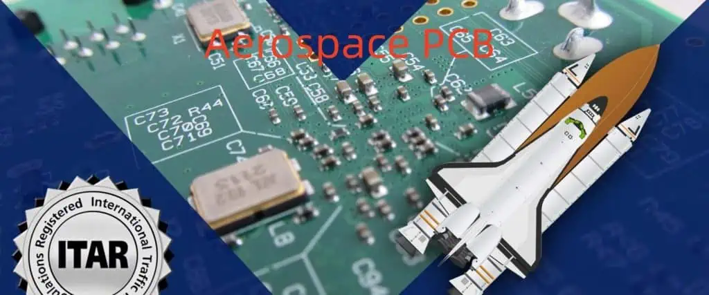
An integrated circuit (IC) is a tiny collection of electronic components and circuits that have been implanted or diffused onto the surface of a single silicon chip or crystal. Because all parts, circuits, and base material come from one piece of silicon, the device is an integrated circuit.

The complexity of ICs ranges from basic logic modules and amplifiers to full-fledged microcomputers with millions of components. They have replaced vacuum tubes and transistors as the main building blocks of practically all electronic devices thanks to their low cost, excellent durability, low power consumption, and fast processing speeds. Although hydraulic, pneumatic, or mechanical controls were traditionally ideal, integrated circuit microcomputers are now helpful as equipment controllers, machine tools, vehicle operating systems, and other applications.

We may also update them without requiring the control circuitry to be changed. Finally, they are so cheap that they may even in electronic toys for kids.

YouTube video

Materials used in manufacturing integrated circuits

chips-bga

Silicon (Si) is the foundation of most modern electronics, powering everything from supercomputers to smartphones to air microwave ovens. It is an essential element because it is a semiconductor, which means that under certain conditions, it conducts electricity while acting as an insulator under others. Doping may change the electrical characteristics of silicon, making it a suitable material for building transistors that amplify electrical impulses. It is also a plentiful element on the planet, making it both economical and desirable. Gallium Nitride (GaN), which can work at higher voltages and is more tempting for high-speed high-power transistors for wireless applications, is not the sole element helpful in electronic devices.

Engineers have constantly found methods to improve silicon devices. Thus the benefits of utilizing silicon appear to expand year after year. Most of the electrical equipment you use daily would not be conceivable without silicon and silicon wafers.

Fabrication Techniques

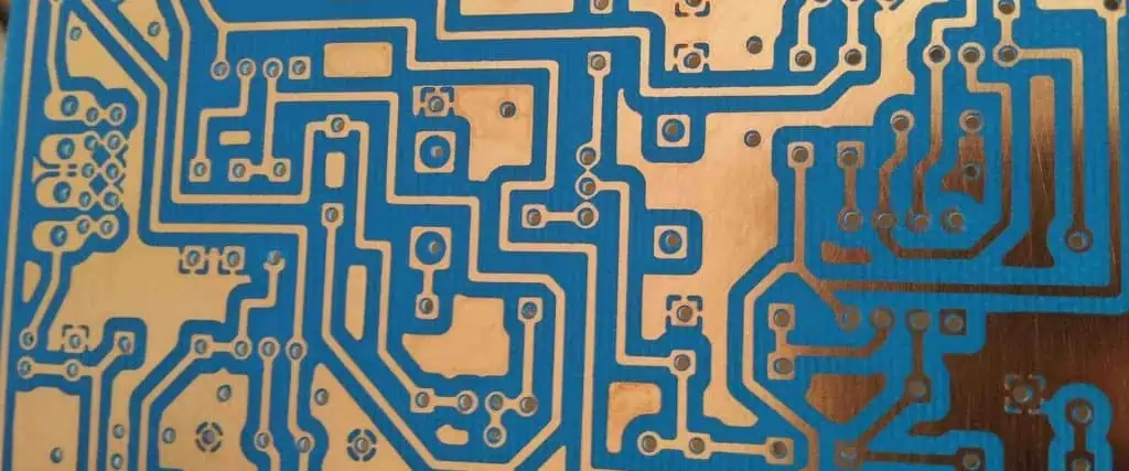
An integrated circuit is normally created by a series of processes, each adding or removing material layers to achieve the required structure. The complementary metal-oxide-semiconductor (CMOS) process, which uses p-type and n-type silicon, is the most widely used manufacturing method for ICs.

A substrate, a thin silicon slice that acts as the IC’s base, is made as the first stage in the CMOS process. Monocrystalline silicon, a very pure silicon, is often used as the substrate.

After substrate preparation, we apply silicon dioxide (SiO2) as a layer on top. This layer acts as an insulator by blocking the passage of electrical current between various IC components.

After that, we decorate the silicon dioxide layer with designs using photolithography. This procedure exposes certain layer regions to UV light using a mask. Finally, we can remove the unexposed parts using a chemical etchant because the exposed areas become less resistant to chemical etching.

After making the designs, we dope the silicon to introduce impurities. Doping intentionally adds trace quantities of other substances to silicon, such as boron or phosphorus. Under specific circumstances, these impurities change the silicon’s electrical characteristics, allowing it to conduct electricity.

The silicon dioxide layer will make metal connections as the process’ follows the stage. Several IC components may send and receive electrical impulses thanks to these connections. Sputtering is commonly helpful to deposit a thin metal layer, such as aluminum or copper, on top of the silicon dioxide layer. The appropriate contacts are subsequently patterned onto the metal layer using photolithography.

The IC is then covered with a passivation layer to shield it from external elements, including moisture and mechanical stress. Often, silicon dioxide or silicon nitride is essential in creating this layer.

The manufacturing process of integrated circuits

FULL PCB MANUFACTURING Quote

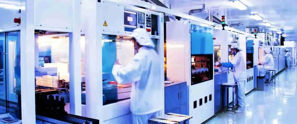
Creating many layers of materials on a substrate to create a functioning electronic device is a complicated procedure for fabricating integrated circuits (ICs). The procedure might take a few weeks and calls for specialized tools, sterile rooms, and qualified workers.

Wafer Preparation

A crucial procedure in the production of integrated circuits is wafer preparation. It entails several steps to create a smooth, clean, and defect-free surface on a silicon wafer. A silicon crystal must first grow before being sawed into thin wafers with a diamond saw. We then carry out the process of wafer lapping using a device that uses a spinning abrasive pad to scrape the wafer’s surface. The final step in producing a mirror-like quality is chemical mechanical polishing (CMP), which removes any last-minute surface flaws.

Combining wet and dry cleaning techniques helps to clean wafers. Before being dispatched for additional processing, we dry the wafer using a hot plate or oven to eliminate moisture. To reduce the possibility of contamination, wafer preparation is a meticulously regulated and supervised operation that we must do in a cleanroom setting.

Oxidation

The wafer’s surface is then oxidized to form a thin silicon dioxide coating (SiO2). The oxide layer protects the silicon beneath from contamination by acting as an insulator for the IC. The oxidation process is a necessary step in the fabrication of integrated circuits. As a result, a thin layer of oxide forms on the surface of a silicon wafer.

This oxide layer is an insulator and a barrier to prevent undesired impurity penetration into the silicon. Pre-cleaning, dry oxidation, wet oxidation, annealing, surface preparation, and thickness measuring are all part of the oxidation process. Because the quality of the oxide layer is essential to the performance of the integrated circuits created atop it, we monitor the process to ensure that it fulfills tight criteria.

Photoresist Coating

A photoresist is a light-sensitive substance used to produce patterns on a wafer. The photoresist coating process is an essential step in producing integrated circuits. It entails covering the silicon wafer with a photoresist. This photosensitive substance functions as a mask to specify the integrated circuit pattern that we will etch onto the wafer. Next, a spin coater helps to apply the photoresist layer to the wafer’s surface. We then bake it at a low temperature briefly to eliminate any solvents and evaporate any leftover moisture from the coating process.

After exposure, we bake the wafer again at a higher temperature to stabilize the photoresist pattern. Then we immerse the wafer in a developer solution, which dissolves either the exposed or unexposed photoresist depending on the photoresist employed. The process happens in a cleanroom environment to reduce the possibility of contamination. Finally, a spin coating procedure helps to apply the photoresist, which uniformly distributes the material throughout the wafer.

Etching

Microelectronics Manufacturing

Etching is vital in producing integrated circuits, which help make electronic devices such as microprocessors, memory chips, and sensors. The etching technique includes selectively removing material from a substrate via a chemical or physical reaction.

So, we initially coat the substrate (often silicon) with a layer of photoresist, a light-sensitive substance that hardens when exposed to light. After that, we put a photomask on top of the substrate and beam light through it. Light-exposed portions of the photoresist become hardened, while unexposed parts remain soft.

We subsequently immerse the substrate in an etching solution, eliminating material from the portions not covered by the hardened photoresist. Wet etching, which employs a liquid solution, and dry etching, which uses a plasma, are the two basic etching methods.

After the etching process, we remove the excess photoresist from the substrate using a chemical stripping solution.

We perform this technique several times on the substrate to generate numerous layers of circuitry. Each layer forms using a distinct photomask and etching method, enabling the creation of elaborate circuitry designs on a very small scale.

Doping

Doping is a critical technique in the fabrication of integrated circuits (ICs) that includes the addition of impurities to particular portions of a semiconductor material to affect its electrical characteristics. The doping process aids in forming semiconductor areas with either an excess of electrons (n-type) or an excess of holes (p-type), which are necessary for fabricating different IC components such as transistors, diodes, and capacitors.

Doping typically entails introducing a tiny quantity of dopant atoms into the semiconductor material using one of many processes, including ion implantation, diffusion, or epitaxy. The application and the required electrical characteristics of the resultant semiconductor area determine the dopant utilized.

In n-type doping, for example, atoms with one more valence electron than the semiconductor material, such as phosphorus or arsenic, go into the semiconductor material. These additional electrons are free to move about and contribute to the material’s conductivity, increasing the number of electrons in the semiconductor area.

Similarly, in p-type doping, atoms with one fewer valence electrons than the semiconductor material, such as boron or gallium, go into the semiconductor material. These missing electrons form “holes” in the material, which are positive charge carriers, increasing the number of holes in the semiconductor area.

The doping process is an essential stage in the production of integrated circuits since it allows for synthesizing the components needed for the circuit to work properly. Therefore, careful control of doping amounts and locations is necessary to guarantee that the resultant IC performs consistently and effectively.

Deposition

Deposition is a method of depositing thin sheets of material onto a substrate, commonly a silicon wafer, in the fabrication of integrated circuits (ICs). This is a vital phase in manufacturing integrated circuits that involves depositing metals, oxides, and semiconductors. Deposition techniques include physical vapor deposition (PVD), chemical vapor deposition (CVD), and atomic layer deposition (ALD).

PVD deposition involves vaporizing a solid source material in a vacuum and allowing it to condense onto the substrate. The process usually happens in a vacuum chamber, where the substrate heats to a high temperature. Then, we blast the source material with ions or electrons, causing it to evaporate and deposit onto the substrate.

CVD, on the other hand, is the chemical interaction between a gas-phase precursor and the substrate surface that results in the deposition of a material onto the substrate. Then, the precursor gas goes into a reaction chamber. Here, it interacts with the surface of the substrate to generate a thin coating of the desired material.

ALD is a more accurate variant of CVD in which materials are deposited one atomic layer at a time. The technique includes exposing the substrate to two or more precursor gases in succession, depositing one atomic layer of the desired material at a time.

Deposition is an important step in the fabrication of integrated circuits because it dictates the characteristics of the thin films that make up the various layers of the IC. Therefore, we must accurately regulate the thickness, composition, and regularity of these layers to guarantee the appropriate operation of the IC.

Planarization

Chemical mechanical planarization (CMP) is vital in today’s consumer and industrial electronics scene. It offers unparalleled topographical consistency for high-precision electronic wafers, establishing the framework for subsequent etching or deposition procedures.

Silicon (Si) is a good semiconductor material because of its unique electron structure, which allows it to establish perfect covalent connections with other atoms. Silicon’s semiconducting qualities make it excellent for producing diodes, transistors, microelectronics, and other devices. It is the most probable material to usher the electronics industry into the age of systems-on-chips (SOC) and ultra-large-scale integration (ULSI) (ULSI).

Engineers are continually engaging with suppliers to swiftly design innovative solutions that fulfill the demands of device downsizing. We can credit this to rigorous control of silicon wafer planarity down to the sub-nanoscale.

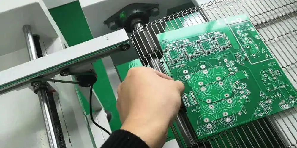
Cleaning and Inspection

Cleaning and inspection are critical steps in the production of integrated circuits. Wet and dry cleaning procedures, optical examination, electron microscopy, and X-ray imaging are Ideal. If we discover them, we rectify defects utilizing several processes, such as laser annealing or chemical etching. When the repairs are complete, we examine the wafers again to confirm that we eliminate all problems. We carefully monitor the process to ensure wafers fulfill stringent quality criteria before manufacturing circuits.

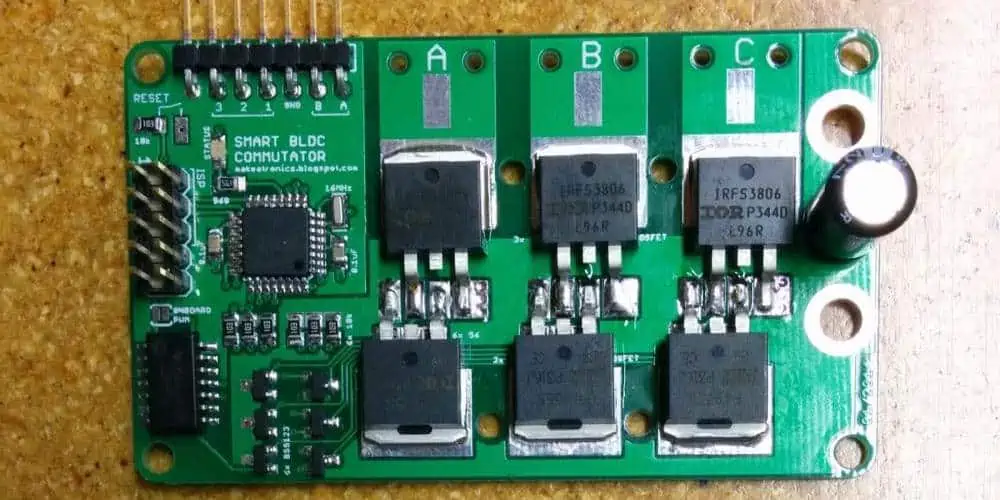
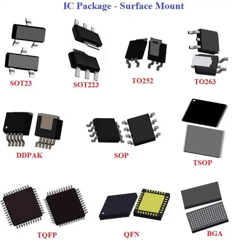
Packaging and Testing

manufacture semiconductor

In the production of integrated circuits (ICs), the packaging and testing process is critical. this is because it entails encapsulating and confirming the functionality of the ICs. This procedure is as follows:

Die preparation is the singulating individual dies from a wafer containing several ICs. This is possible by cutting or scribing the wafer along preset lines, separating each die from the wafer.

Die attachment: Using a die-bonding machine, the individual die bonds to a lead frame or a substrate at this point. This machine employs conductive adhesive.

Wire bonding: use a wire-bonding machine to link the die to the lead frame. The wire-bonding machine uses ultrasonic energy to connect a tiny wire from the bonding pad on the die to the lead frame.

Encapsulation: We enclose the IC in a protective container after wire bonding to protect it from external elements such as moisture, dust, and mechanical damage. Encapsulation materials are generally thermoset plastics or ceramics.

Testing: When encapsulating the IC, we subject it to a series of tests to confirm its functioning. Functional testing, performance testing, and reliability testing are all possibilities. These tests guarantee that the integrated circuit fulfills the specified requirements and standards.

Marking and sorting: After passing all tests, we label the IC with a component number, lot number, and date code. We then sort the integrated circuit depending on its speed, temperature range, and packaging type properties.

Final inspection: We scrutinize the IC for faults like scratches, cracks, or other physical problems at the final inspection step. This will guarantee that the IC satisfies the quality criteria necessary.

Conclusion

Finally, due to its unique electrical characteristics, silicon is the most extensively helpful material for constructing integrated circuits. Silicon is a semiconductor, meaning it may conduct electricity under certain conditions. Additionally, we can adjust its conductivity by introducing impurities. Silicon is also extremely stable and corrosion-resistant, making it a perfect material for use in electrical equipment.

PCB Ecuador, the Promising Market

hdi high density interconnect PCB

Have you ever pondered the nature and operation of a printed circuit board? Or what its different forms and uses are? Learn everything there is to know about printed circuit boards in Ecuador and their applications, including the design phase, the assembly process, and the best PCB manufacturing, importing and supplying companies in the country. What benefits are there to using an Ecuadorian PCB manufacturer? What advantages do flexible PCBs offer? And how does a rigid-flex PCB provide more complexity and flexibility?

What is a Printed Circuit Board?

A printed circuit board (PCB) is a type of electronic board we use to support and contain electrical and electronic components securely. Typically, it is useful in the production of electronic devices such as computers, laptops, tablets, cell phones, and other electronic gadgets. First, you set a layer of copper foil on top of the non-conductive materials, which are typically plastic or fiberglass. Next, etch the copper layer using a chemical etching procedure to generate the appropriate circuit layout. The process permits the creation of intricate and sophisticated circuit designs that are effective in terms of current circulation in electrical gadgets.

You then solder the copper foil to the components on the board, making a permanent connection. The connection enables current flow across the elements creating the desired electrical circuit. The PCB supplies the required quantity of electricity to the circuit’s components, which often demand a specific amount.

Because of their suitability for intricate and complex circuitry, PCBs have enabled the development of a vast array of consumer devices. Moreover, they are also useful in industrial and military applications since manufacturers can make them extremely durable and resistant to extreme temperatures, vibration, and shock.

Moreover, manufacturers utilize them to make integrated circuits (I.C.s). On a single chip, an integrated circuit contains thousands of transistors and other components. Technicians use PCBs to establish an electrical connection between the integrated circuit and the surrounding components. Doing so enables the integrated circuit to fulfill its intended function.

Generally, PCBs are integral aspects of the electronics industry since they enable secure component support and connection. Moreover, this allows the creation of complex and complicated circuits, which enables the production of a vast array of consumer electronics. Technicians also use them in industrial and military applications due to their reliability and longevity.

Applications of Printed Circuit Boards

heavy copper pcb circuit board

Printed circuit boards are applicable in various industries and applications due to their electrical and mechanical capabilities. Moreover, they are most useful in linking electronic components, but they also have a range of other applications. Generally, these components are primarily useful in consumer electronics, medical devices, automotive applications, and industrial applications.

Printed circuit boards operate in everything from computers and phones to smartwatches and other wearable devices in consumer electronics. Typically, several components, including resistors, capacitors, transistors, and integrated circuits, are soldered on the PCB. Then, you interconnect the parts to form a control circuit (CC) for the gadget.

PCBs have multiple applications in the medical industry. Technicians use them to monitor and control medical equipment such as X-ray and MRI gadgets. In addition, they are useful in monitoring the patient’s vital indicators, including:

  • temperature,
  • heart rate
  • blood pressure.

PCBs are also applicable in automobile navigation systems, cruise control systems, and engine management systems. In this industry, printed circuit boards operate impeccably to regulate the many vehicle systems, including brakes, engine, and transmission. Moreover, Printed circuit boards also manage a variety of industrial machinery, from automated assembly lines to CNC machines. In addition, they operate to monitor and regulate numerous industrial processes, such as temperature and pressure control.

Printed circuit boards have various applications and are applicable to nearly every electronic gadget that you might come across. Typically, they are dependable, inexpensive, and simple to make. Moreover, due to their extensive range of applications and characteristics, they are an indispensable component in various sectors and applications.

Types of Printed Circuit Boards

FULL PCB MANUFACTURING Quote

Electrical and electronic equipment must have printed circuit boards because they enable the connecting of various components into a single unit. Printed circuit boards come in multiple designs, each with unique features and capabilities. These varying types of printed circuit boards include the following standard PCB designs:

Single Layer PCBs

The single-layer board is the most typical kind of printed circuit board. We print an electrical circuitry pattern on a single sheet of conductor, often copper, to create this kind of board. The single-layer board is the simplest and least expensive type of printed circuit board. It is generally useful in low-power devices like calculators and LED lights.

Double Layer Printed Circuit Boards

Another variety of printed circuit boards is the double-layer board. Technicians print a pattern of electrical circuitry on each of the two layers of this sort of board, which is made of conductive materialโ€”typically copperโ€”in two layers. While costing more than a single-layer board, a double-layer board offers more versatility and intricacy. Typical applications for this kind of board include more sophisticated electrical appliances like computers and smartphones.

Multilayer Printed Circuit Boards

The most complicated kind of printed circuit board is one with multiple layers. It contains numerous layers of conductive materialโ€”typically copperโ€”each of which has an electrical circuitry pattern printed on it. These types of boards are applicable in high-power applications like automotive engines as well as complicated electrical equipment like computers and mobile phones.

Flexible Printed Circuit Boards

The flexible printed circuit board is a specific kind of printed circuit board with a flexible material, such as polyimide. Flex circuit boards are great when weight or space are issues because they are lightweight and robust. In addition, medical equipment and other uses that call for flexibility also use flexible printed circuit boards.

Rigid-Flex Printed Circuit Boards

We refer to a combination of rigid and flexible printed circuit boards as a rigid-flex PCB. Technicians print a PCB design of electrical circuitry on each layer of the rigid material (which is often copper) in this sort of circuit boards. The rigid-flex board costs more than the other board varieties, however it offers more flexibility and complexity, which ultimately enables the integration of various components that wouldn’t otherwise be applicable in board designs. You can find rigid printed circuit boards in everything ranging from cellphones to calculators and wearables.

Printed circuit boards come in a wide variety of designs, each with unique features. The single-layer board is the least complex and ultimately the most affordable sort of printed circuit board, whereas the multi-layer board is the most complex and hence the most expensive. The rigid-flex and flexible printed circuit boards provide more flexibility and complexity, enabling the integration of components that would not otherwise be conceivable

The PCB Assembly Process

Soldermask and Silkscreen Process of Aluminum PCB Manufactturing

Printed circuit boards (PCBs) are essential parts of many electronic products, from high-end medical equipment to home appliances. A printed circuit board is assembled using multiple discrete processes that require technicians to pay great attention to detail.

Designing Phase

The PCB design is the first phase, which entails utilizing specialist software programs such as CAD to design a schematic of the board that lists the elements you must install and the connections you must make between them. After the schematic is complete, you must generate a layout to specify the precise dimensions and placement of the parts and paths.

Component Gathering

The technicians must then order the components applicable to the PBC assembly process. These components comprise all of the required resistors, capacitors, integrated circuits (I.C.s), and other parts. The ordered parts are then sent right away to the assembly plant.

PCBA

The PCB is populated with the required components once the components have been received via manually or automatically soldering the components into position. Moreover, soldering is essential to ensure that all components are firmly in place and that there is no danger of short or other potential problems.

Lastly, you must examine the PCB to ensure it is operating correctly. Technicians take the PCB through a set of tests to ensure that everything is functioning as it should and that there are no defects or other mistakes in order to do this.

Printed circuit board assembly is challenging and demands close attention to detail. Therefore, it’s crucial to check that the board is operating correctly. Technicians must rework or scrap the board if they find mistakes throughout the testing procedure. These procedures create a high-quality PCB that can endure the demands of use.

The Best PCB Manufacturing, Importing, and Supplying Companies in Ecuador

Ecuador is home to some fascinating PCB manufacturing companies committed to providing impeccable PCB manufacturing services. These companies include:

Solintece Cia LTDA

Ecuador-based Solintece Cia. Ltda is a PCB manufacturer that offers its clients items of the highest caliber at reasonable prices. Since its founding in 2010, the business has developed into a top supplier of Printed Circuit Boards (PCB) for various uses in the electronics sector.

Single-sided, double-sided, and multilayer PCBs, flexible, stiff-flex, and rigid PCBs, as well as high-frequency, high-speed, and high-density PCBs, are all available from the company. Moreover, the company also offers SMT assembly and testing services and impeccable design services.

The firm is dedicated to giving its customers the highest caliber goods and services. Moreover, the company’s highly skilled engineers and technicians work hard to deliver the most significant technical assistance and the highest levels of quality assurance to you. The business has a quality management system (QMS) that ensures all of its goods and services adhere to the highest industry standards and is ISO 9001:2015 certified hence you can expect goods of the highest quality from them eveytime.

Due to its broad global partner network, Solintece Cia. Ltda can offer consumers the best goods and services in the shortest amount of time. Also, the business employs a skilled group of salespeople who are constantly available to assist clients with their unique requirements.

The business is committed to giving its clients the highest possible return on their investment. Several clients love it because of its incredibly competitive prices and top-notch customer service. Additionally, it provides tailored solutions to satisfy specific client needs.

Generally Solintece Cia. Ltda aims to offer cutting-edge goods and services that satisfy its clients’ changing needs. It continuously seeks fresh approaches to enhance its goods and services to stay ahead of the competition. The business is dedicated to giving its clients the highest caliber goods and services at the most affordable costs.

DHL express Ecuador SA

Global PCB exporter DHL Express Ecuador S.A. belongs to a broader worldwide network of DHL Express enterprises and is the nation’s top provider of international express and logistics services. The company is primarily renowned for providing high quality PCBs to clients worldwide in a dependable and effective manner.

The Overview and Functionality

Since its founding in the early 2000s, DHL Express Ecuador S.A. has developed into one of the nation’s biggest and most well-known exporters of PCBs. The business provides a broad range of services to fulfill the demands of the global market. It offers PCB delivery, custom packaging, freight forwarding, and customs clearance to you as their customer.

The business aims to offer top-notch customer service and high-quality goods. You can be sure of the highest standards in quality and safety thanks to its ISO 9001 and 14001 certifications. The employees at DHL Express Ecuador S.A. are committed to providing clients with PCBs that are delivered effectively and on schedule. Therefore, you can expect to get your order in time.

The business has invested in infrastructure and technology to guarantee the timely and accurate supply of printed circuit boards. Throughout the delivery process, its sophisticated tracking system is intended to keep consumers updated on the status of their packages. Also, customers have online access to their tracking data, enabling them to track the status of their shipments in real-time.

Also dedicated to sustainability and environmental preservation is DHL Express Ecuador S.A. It has put into place several steps to lessen its environmental impact and carbon footprint. The business also adopted an energy efficiency program, which resulted in a 30% decrease in energy use and emissions.

Printed Circuit Boards are delivered consistently and expertly by DHL Express Ecuador S.A. to clients throughout the globe. Customers receive their products on schedule and in pristine shape because of the company’s dedication to quality and effectiveness. In addition, the company’s commitment to sustainability assures that it is contributing to environmental protection and lowering its carbon impact.

Conclusion

In conclusion, printed circuit boards are essential components of numerous electronic gadgets used in various fields and applications. Moreover, the top PCB manufacturing and delivery businesses in Ecuador are Solintece Cia LTDA, and DHL express Ecuador S.A., both of which provide high-quality services, products, and client support. Their dedication to impeccable sustainability, quality, and customer happiness is evidence of how crucial printed circuit boards are in the society of Ecuador.

Everything you need to know about PCB Manufacturer Romania

Customized rigid flex PCB

The PCB or printed circuit board industry is growing in a consistent manner. Actually, experts estimate that this market will have a net worth of over 89 billion USD by the end of 2024. However, such growth means that multiple investors are diverting their money into investing in PCB manufacturing firms spread out across the world. But, even though there are numerous PCB manufacturing firms in the world, not all of them provide impeccable PCB manufacturing capabilities.

If you are living in Romania, you probably know that this area has a lot of PCB manufacturers. However, do all these manufacturers provide high-quality outputs and services? Obviously no. So which are the best PCB manufacturing companies in Romania? And why should you work with these companies to make your PCB project successful?

Printed Circuit Boards in a Nutshell

universal pcb
universal pcb

Printed circuit boards or PCBs are sheets of insulating components with metallic tracks or circuits attached to them for impeccable electrical conductivity. Since their invention, printed circuit boards have become pretty popular due to their ability to help manufacturers generate compact, powerful gadgets. As per the 21st century, you can find PCB in most, if not all, electronic components, for example, keyboards, smartphones, wearables, satellites, military gadgets, medical gadgets, etc.

Printed Circuit Board Assembly

Whether you require a single PCB or multiple printed circuit boards for your project, outsourcing the printed circuit board assembly process to experts generally yields better results than when you try to make the circuit board independently.

Therefore, you should highly consider working with PCB manufacturing companies to guarantee high-quality printed circuit boards. These companies utilize high-tech gadgets to generate PCBs with higher precision. Moreover, by following set standards, these companies are consistent in terms of quality.

Moreover, working with a PCB manufacturing company doesn’t just assure you that the product you get back will match your quality requirements and strict specifications. It also comes with multiple advantages, which include more durable PCBs and reduced costs of production. Moreover, since most manufacturers have strong relations with top-tier suppliers, they can get high quality products without breaking a sweat.

The Best PCB Manufacturer in Romania

FULL PCB MANUFACTURING Quote

BAM Prototypes

BAM Prototypes, a PCB manufacturer headquartered in Romania, specializes in providing trustworthy, high-quality PCB solutions for several industries. The company offers impeccable services and has more than ten years of experience in the PCB sector.

BAM Prototypes specializes in manufacturing pretty complex, multilayer, high-throughput PCBs utilizing a variety of technologies. Moreover, the company is committed to providing its customers with the highest level of quality and precision while keeping reasonable prices. In addition, BAM Prototypes offers PCB-related services, including design, prototyping, fabrication, assembly, and testing, to customers needing help with their PCB needs.

Surface mount technology (SMT) and automated optical inspection are merely two of the newest technologies used in the company’s highly efficient production process (AOI), which ensures the timely delivery of a high-quality product to the user. In addition, BAM Prototypes are ISO 9001-certified, meaning it meets the highest quality and reliability standards.

In addition to its production capabilities, BAM Prototypes offers a vast array of PCB-related services to help customers, which includes testing, design, and technical support services. Doing so allows customers to optimize the usage of their boards.

Overall, BAM Prototypes is a respectable and reasonably priced PCB manufacturer that provides various services to meet the client’s needs. Clients can rely on BAM Prototypes to supply them with the best possible PCB solution due to the company’s commitment to quality and reliability.

Circuit Design SRL

Romania is home to the famous PCB maker Circuit Desing SRL.

The company has grown to be one of the most recognized PCB manufacturers in the area since its foundation in 1991.

The company caters to several industries and specializes in the production of rigid, flexible, and hybrid PCBs.

The business is committed to offering customers products of the highest quality and economical solutions.

They are dedicated to meeting consumer demands and ensuring their satisfaction.

To achieve this, they use cutting-edge manufacturing techniques and top-quality materials.

As a result, they can create durable PCBs for a range of applications. Circuit Desing SRL also offers a variety of different services. These services include mass production, component buying, custom design, and prototyping.

They also provide technical support and consulting services to assist customers in getting the most out of their PCBs.

The company is dedicated to reducing its operations’ environmental impact and has a solid commitment to impeccably sustainable production.

They actively contribute to creating environmentally friendly solutions, such as using recyclable packaging and lead-free construction materials. The PCB manufacturer Circuit Desing SRL is pretty well-known and renowned. Moreover, they are in an excellent position to meet the needs of Romanian customers because of their commitment to quality, sustainability, and customer pleasure.

Electro Promex Invest EBS Group

Electro promex is a famous PCB manufacturing company that is situated in PetroSani in Romania. Compared with other companies, this PCB manufacturing company stands out due to its ability to provide comprehensive PCB products. Through the utilization of high-tech gadgets, this company produces lighting solution printed circuit boards, sensor PCBs, and IoT printed circuit boards. Moreover, this company’s multilayer printed circuit board capacity is typically fully fledged.

Additionally, apart from providing PCB products, this company also majors in the provision of printed circuit board design services to its clients.

ElectroMagnetica S.A

PCB motor design
PCB motor design

ElectroMagnetica, which is commonly known as EMS, is a Romanian-based PCB manufacturing company that is situated in Bucharest. The company employs many young IT employees who bring new innovative ideas to the table. Moreover, this company handles electronics subassembly and assembly services instead of solely focusing on printed circuit boards.

EMS mainly produces the following products:

EMS Electrical SRL

Before moving to Romania, this organization was a branch of a famous German corporation. EMS electrical SRL doesn’t produce PCBs as commodities. Instead, they provide printed circuit board assembly services, printed circuit board assistance, and printed circuit board design services.

However, if you want to buy a ready-made PCB, you can do so via their sister company, PCB Electra.

Kimball Electronics

Kimball electronics is another famous Romanian-based PCB manicuring company situated in Timisoara. The company typically majors in turnkey PCB solutions. Kimball electronics can efficiently perform the following services to clients:

  • New product integration
  • Design services
  • Diversified CMS services

Moreover, some clients utilize this company to effectively test their gadgets. For example, this company serves significant companies in the medical sector. Therefore, in terms of quality, and precision, Kimball has got you covered.

Mibatron

Mibatron is a PCB manufacturing form that has the ability to produce thick PCBs containing up to 10 layers. Moreover, this company also makes the following PCBs:

  • Double-sided PCBs
  • Single-sided PCBs

However, this company is primarily famous because of its EMS services. The company has been in the PCB Industry for over 30 years. Therefore it has impeccable experience.

Compared to most Romanian PCB manufacturing companies, this company is pretty conservative. However, even with this conservative factor, Mibatron is still pretty dependable.

PCB Electra

PCB Electra is a famous Romania PCB manufacturing company that has its headquarters in Bratuleni-Miroslave. The company is in pretty good condition, and it has been running for over 15 years, offering high-quality printed circuit boards to clients. Moreover, PCB Electra provides a lot of products which include:

  • Peelable solder mask printed circuit boards
  • 4-layer printed circuit boards
  • ENING printed circuit boards, also known as hard gold printed circuit boards

PCB Electra primarily utilizes two types of materials to generate printed circuit boards, which are the following:

Phoenix PCB

Phoenix PCB is a famous and prominent PCB manufacturing company that mainly produces rigid printed circuit boards. Actually, this company doesn’t create flex or rigid-flex printed circuit boards.

With its multiple surface finish options, this company can offer lead-free printed circuit boards at affordable prices. However, they primarily utilize HASL.

Phoenix PCB is pretty good when it comes to handling low-volume PCB orders. Therefore, if you are looking for a PCB manufacturing company in Romania to handle your PCB prototype, then this company can help you. Moreover, this company has multiple loyal customers in Romania. Therefore you can trust them with your order.

Symph Electronics

Symph electronics is another famous PCB manufacturing company situated in Timisoara in, Romania. The company utilizes impeccable tech and highly trained employees to deliver:

However, when it comes to generating PCBs, Symph is somewhat limited. However, they still provide their impeccable services as an OEM. When it comes to PCB assembly, this company can do the following:

  • Surface mounting
  • And through hole plating of electrical components

Why should you work with a Romanian PCB Manufacturer?

Upcoming and old printed circuit board manufacturing companies benefit significantly from setting their roots in Romania. That is because Romania has a pretty stable political environment and a sane legal system. Moreover, PCB manufacturing companies in Romania tend to enjoy talented and young workforce support. Here are more reasons why you should work with a Romanian PCB manufacturing company.

Promising Logistics Hub

Businesses and firms looking for different Asian PCB sources are now flooding Romania to do business with Romanian PCB manufacturers. Moreover, Romania competes with Poland in terms of quality and prosperity of life even though Poland has a tremendous local river. Therefore, Romania is pretty efficient in terms of utilizing its resources. Actually, Romania is an excellent alternative to polish printed circuit board manufacturers due to their common trade routes and shared geo-locations. Therefore, if you use a Romanian PCB manufacturer, you get to experience the convenience that comes with a Polish circuit board maker, but at the same time, you get to save a lot of money.

Low Taxes

Most companies choose Romania since carrying out business in this country tends to be less expensive. Typically, Romania only levies around 16% in terms of corporate income tax. However, in other developed countries, for example, China and Poland, these rates can go as high as 25%.

Lower tax rates typically translate to cheaper printed circuit board production. Therefore, when you work with a Romanian PCB manufacturer, chances are you will get high-quality printed circuit boards at relatively lower prices. Moreover, since they get to save in terms of expenditure, they invest in this money in getting high quality components that they use to make your products at reasonably low prices.

Many Industry Parks

Industrial Parks situated in Romania typically attract business into the country. The main reason why these industrial parks attract business is because of the dedicated utility connections found in these areas. Moreover, these areas are generally great for the establishment of companies.

These industrial parks have impeccable infrastructures, are more secure, and provide people working in this area with impeccable transportation.

You will primarily find these components in the southern region of Romania. Moreover, most of these components are dedicated to the information tech, construction, and aerospace industry.

Young and Talented Workforce

Research shows that most Romanian workers have impeccable skills and are good at what they do. Moreover, the workforce in Romania is typically full of motivated youthful individuals who are more than willing to work well in the printed circuit board industry. Additionally, these individuals can efficiently communicate with clients from Europe and Russia since most are multi-lingual.

The government of Romania also supports individuals in the PCB industry by offering high-quality educational training via their “technical vocational training and education” program that is entirely free for Romanian citizens. Using this educated workforce, PCB manufacturers are able to tap reliable employees.

Conclusion

In conclusion, the PCB manufacturing industry in Romania has a lot to offer. From impeccably high-quality productions to low tax rates, the Romanian PCB manufacturing businesses are undoubtedly worth considering. Moreover, these organizations are well established, utilize the newest technologies, and have a talented and dedicated workforce. As such, they are more than capable of generating reliable and high-quality printed circuit boards.

How to Get a Good and Fast PCB Assembly Quotation?

PCB assembly house in Austria

An estimate of the cost to assemble electronic components onto a printed circuit board is known as a PCB Assembly quotation, which is given to a client by a PCB Assembly service provider (PCB). It is a crucial stage in the PCB assembly process since it gives customers a rough idea of how much their project will cost and enables them to plan their production accordingly.

The quotation for PCB assembly frequently includes details like the cost per unit, the cost of the materials, the turnaround time, and any additional fees or costs for services like component sourcing, PCB testing, or conformal coating. The customer’s particular PCB design specifications, component needs, and PCB quantities determine the price.

The documents needed to obtain a PCBA quotation

You normally need to give the PCB Assembly service provider several papers and project parameters to get a PCB Assembly (PCBA) quotation. The following are some of the crucial documents you would need to provide to get a PCBA quote:

Bill of Materials (BOM):

A complete inventory of all the parts and supplies needed to produce or assemble a product is known as a bill of materials (BOM). It is a key document used in manufacturing and supply chain management that contains all the details required for product procurement, construction, and maintenance. It can be produced at different points along the product development cycle, from the preliminary design stage to the last production stage. Depending on the particular requirements of the manufacturer, we can structure a BOM in various ways. The engineering BOM, which includes all parts and supplies required to make the product, is the most typical.

During the production phase, a manufacturing BOM is necessary, and it may include containing extra data like assembly instructions, labor and equipment expenses, and other production-related information. It is a vital tool for supply chain management and ensuring that the appropriate components are accessible when needed. As a result, manufacturers may streamline their production procedures, boost productivity, and cut costs using a BOM.

Gerber files:

A common file format used in producing printed circuit boards is called Gerber (PCBs). They provide machine-readable data on the copper layers, solder masks, and other elements of the PCB design. Usually, the PCB maker receives them from the PCB design software. We use them to develop the circuit board layout and use them to produce the actual board. Gerber files consist of several layers. They include silkscreen, drill, and board outline layers, as well as layers for copper and solder masks. Each layer has a collection of vector shapes, such as lines and polygons, which specify its unique properties.

They are well-known by most PCB makers globally and are frequently helpful in the industry. Gerber files enable manufacturers to swiftly and effectively create high-quality PCBs while guaranteeing that they satisfy the demands of their clients.

Assembly drawings:

These designs describe the electronic components’ location and orientation on the PCB in detail. Moreover, they could have guidelines for soldering and component placement.

Testing specifications:

To verify that the PCB Assembly service provider can satisfy your requirements, you should supply them with particular testing requirements if you have any for your project.

Quantity and delivery requirements:

The number of PCBs necessary for the project must be available to the PCB Assembly service provider. additionally, any special delivery specifications like deadlines or shipping guidelines.

Include any additional requirements or specifications

Include any additional requirements or specifications in your documentation if your PCBA project has particular demands or specifications, such as conformal coating or custom packaging.

In general, the more accurate the PCBA quotation you obtain, the more thorough and comprehensive your paperwork is. To ensure clarity, it is also crucial to maintain clear communication with them throughout the process.

Missing Information when Requesting a PCB Quotation

FULL PCB MANUFACTURING Quote

It’s critical to give the PCB manufacturer to secure an accurate price. Don’t worry if you lack precise details; most PCB manufacturers will work with you to get them. Here are some instances of information that may be necessary from you:

PCB design files: You will need to ask your designer for your PCB design files or Gerber files if you don’t already have them, or you can give the PCB manufacturer particular details about the board’s physical dimensions, layer count, and other requirements.

Quantity and delivery requirements: The PCB manufacturer can assist you in identifying the right quantity and delivery schedule based on the needs of your project if you’re unsure of how many PCBs you need or when you need them.

Material requirements: The manufacturer can give you options based on your requirements, such as FR4, aluminum, or ceramic materials, if you’re unsure of the materials you need for your PCB project.

PCB testing requirements: If you are unsure about the kind of testing needed for your PCB project, the manufacturer can assist you in choosing the right testing strategies based on the specifications of your project, such as functional testing or in-circuit testing.

Special requirements: Be sure to let the PCB manufacturer know if your PCB project has any unique requirements, such as high-temperature functioning or RoHS compliance, so they can ensure their production method satisfies your specifications.

Factors that affect PCB assembly cost

Filling electronic components on a PCB to make a working electronic device is known as printed circuit board assembly. The size and complexity of the PCB, the quantity and caliber, volume, and the testing requirements are only a few of the variables that affect PCBA cost.

PCB size and complexity

The PCB’s size and complexity are the main determinants of PCBA cost. Bigger PCBs demand more resources and processing time, which raises the cost of production. Moreover, more expensive manufacturing processes are needed to produce PCBs with more layers, elaborate designs, and specialty materials.

Component type and quantity

The kind and number of components used in the PCBA process significantly impact the overall price. Through-hole components are less expensive than high-quality parts with surface-mount technology (SMT) or a ball-grid array (BGA). The overall cost rises by using more components in the assembling process.

Assembly technique

The price of PCBAs might vary depending on the assembly method employed. For instance, manual assembly costs more than automated assembly since it requires more time and work. On the other hand, the precision and accuracy of mechanical assembly methods like pick-and-place and surface mount technology (SMT) improve while costs reduce.

Manufacturing volume

PCBA production volume requirements are a significant cost-determining element. The price per unit decreases as the volume increases. This is because fixed expenditures move over more units at a lower cost per unit.

Testing requirements

Cost may vary depending on PCBA testing specifications. To verify that the finished product fulfills the necessary criteria and standards, testing is a crucial step in the PCBA process. For example, in-circuit testing (ICT) and functional testing (FCT) are more expensive than simple testing techniques like a visual inspection. The time needed for production may also extend by testing requirements, which may raise overall costs.

Packaging cost

Another element that impacts PCB assembly prices is packaging cost, and the cost of different electronic component packages will impact those costs. Consider the BGA as an example; it needs more time and energy to complete the package since it must connect to a power supply. Therefore, some components may demand more labor to complete the package. In addition, BGAs must have their electrical pins X-rayed to check for issues like short circuits, which will significantly raise assembly costs.

National Labor Costs for PCB Assembly

Labor costs, which differ from region to region, significantly impact the cost of PCB assembly. For instance, assembly services in low-cost nations can help you save roughly 50% on labor costs. But, while selecting labor from other nations, you should also consider their level of PCB assembly competence, particularly for more challenging PCB assembly projects like multi-layer PCBA.

Lead time

The cost of PCBA may vary depending on the lead time needed. For example, the overall price may rise if the manufacturer must give the order higher priority and devote more resources to achieve the deadline if the lead time is short. Conversely, a longer lead time might give the manufacturer greater leeway to streamline production, reducing costs.

Why you need a PCB calculator?

Anybody involved in designing, prototyping, or producing printed circuit boards will find a PCB calculator a helpful tool (PCBs). It makes it easier to compute several PCB design characteristics rapidly and accurately.

Listed below are some of the causes you might use a PCB calculator:

To ensure compliance with design rules: PCB manufacturers often have design guidelines to follow to ensure that the PCB is effective. You may rapidly determine the proper trace widths via diameters and other design characteristics. They must adhere to the manufacturer’s design guidelines by using a PCB calculator.

To optimize board performance: Trace resistance, voltage drop, and signal integrity, for example, can all impact a PCB’s performance. By calculating these characteristics with a PCB calculator, you may optimize your design to increase board performance.

To estimate costs: The price of producing a PCB might vary depending on its size and complexity. You can use a PCB calculator to estimate the price of your PCB design based on various variables. They include board size, layer count, and component density.

To save time: One must calculate numerous PCB design parameters manually, which can be time-consuming and error-prone. You may save time by automating these calculations and getting precise results with a PCB calculator.

Comparing design possibilities: While creating a PCB, several options for trace widths, sizes, and other design elements may be available. You can use a PCB calculator to assess the performance and cost of these several design possibilities. Additionally, you can select the one that best suits your requirements.

Ways of solving the global shortage of electronic components

circuit board electronic components

A scenario with a strong demand for a specific type of electronic component but not enough supply to satisfy that demand is an electronic component shortage. Several things might cause this problems in the supply chain, and delays in production or delivery.

Consumer electronics, automobiles, and telecommunications are just a few businesses that the lack of electronic components and individual customers may significantly impact. As a result, price rises, product delays, and even production halts may result from scarcity. However, scarcity can also influence the creation of novel goods and technology.

Recent years have seen a particularly severe scarcity of electronic components, with geopolitical tensions and the COVID-19 pandemic adding to interruptions in the worldwide supply chain.

YouTube video

Why is it so hard to get electrical parts?

components manufacturers

There are several reasons why finding electrical parts could be difficult:

Counterfeit products: You risk acquiring fake or inferior electrical parts from unreliable suppliers, which might endanger your safety, harm your equipment, or create system malfunctions.

Complex specifications: Complex requirements for electrical parts may be necessary, requiring certain sizes, materials, and performance qualities. Due to this, it could be challenging to identify acceptable substitutions or alternatives.

High demand: Due to the rise in the usage of electronic systems and gadgets in various sectors, including telecommunications, healthcare, and the automobile industry, electrical parts may be in high demand.

Supply chain disruptions: Worldwide supply chain disruptions brought on by the COVID-19 pandemic have resulted in shortages and delays in the manufacturing and delivery of various goods, including electrical parts.

Limited availability: Due to their particular function, application, or manufacturing method, certain electrical parts could only be available in restricted quantities. For instance, due to security considerations, the supply of specialized components used in aircraft or military applications may be limited.

Most impacted Sectors Affected by the Lack of Electronic Components

FULL PCB MANUFACTURING Quote

The supply of electronic components is greatly affected by the availability of semiconductors in many sectors. These three sectors, in particular, are affected by the shortage:

  • Power/Energy: Construction, a sector that is struggling with other suppliers as well, is hampered by the shortages of electronics components, which also affect LED lighting. It may also impede the development of renewable energy.
  • Smartphone/Tech: The demand for cell phones drastically decreased during the epidemic but is anticipated to rebound. Nowadays, the industry uses around half of the multilayer ceramic capacitors made annually.
  • Automotive: Despite the short-term decline in demand for automobiles, the automotive sector is going through significant developments that are increasing manufacturers’ reliance on the supply of electronic components. More complicated electronic elements that adhere to safety and warranty criteria are necessary for automated systems and sensors that are more advanced. As a result, the requirement for electronic components will increase along with the growth in the market for electric cars.

Solution

Automobiles, consumer electronics, and medical gadgets are just a few of the numerous industries impacted by the global scarcity of electronic components. These are a few strategies for addressing the worldwide scarcity of electrical components:

Diversify Supply Chain

The manufacture of electronic components focuses on a few nations. Examples include such as China and Taiwan, which is one of the primary causes of the shortage. However, reducing the risk of supply chain interruptions is possible by purchasing components from many locations.

There are various ways that supply chain diversification might lessen the worldwide scarcity of electrical parts:

Encouraging Innovation: Moreover, diversification can promote supplier competition and innovation. A better and more diverse supply chain may come from companies working with various suppliers to develop new technology.

Improving Supply Chain Resilience: The robustness of the whole supply chain increases by diversifying it. Businesses might use a range of suppliers from several markets and countries to guarantee that the supply chain can sustain interruptions in one location.

Identifying Alternative Suppliers: The supply chain must be diverse. You can do this by locating and working with various vendors that can deliver the necessary electronic components. This gives businesses additional alternatives and flexibility if a particular provider cannot satisfy their demand.

Reducing Dependence on a Single Supplier: It might be dangerous to rely solely on one source for electrical components since any disturbance in their supply chain could result in a shortage. Therefore, companies may lessen their reliance on a single supplier. Additionally, they lessen the effect of interruptions by diversifying their supply chains.

In conclusion, supply chain diversification may enhance supply chain resilience, promote innovation, and lessen the effects of disruptions. It can also offer alternatives and flexibility. These advantages may eventually aid in easing the worldwide electronic component scarcity.

Increase Production Capacity

The worldwide scarcity of electronic components can significantly reduce by increasing production capacity. However, this may not be a comprehensive answer. Nevertheless, these are some ways that boosting manufacturing capacity might be beneficial:

  • Promote new investments: The sector for electronic components can benefit from new investments by increasing manufacturing capacity. As a result, new technology, new industrial techniques, and more effective supply networks may result.
  • Shorten lead times: The time it takes for a manufacturer to fill an order can shorten with increased manufacturing capacity. This can shorten backlogs and speed up order delivery to clients.
  • Satisfy rising demand: There is a much greater need for electronic components worldwide, and raising production capacity can assist in satisfying this demand.

We may not resolve the scarcity of electronic components by simply expanding production capacity. The following are some more causes of the shortage:

  • Trade tensions: Trade conflicts between nations can impact the manufacture and distribution of electronic components.
  • Rise in consumer electronics demand: The epidemic has also resulted in a rise in consumer electronics demand, which has added stress to the supply chain.
  • Supply chain disruptions: The COVID-19 epidemic has affected the manufacture and transportation of electronic components, disrupting the worldwide supply chain.

A multifaceted strategy is required to overcome the global scarcity of electrical components. Increasing manufacturing capacity, strengthening supply chain resilience, diversifying supply sources, and investing in R&D to create new technologies and production methods are a few examples of how to do this.

Enhance Visibility and Transparency

We can prevent shortages by improving supply chain visibility and openness. As a result, we can accomplish this by utilizing digital technologies. An example is using blockchain to build a transparent and secure supply chain network.

Several ways to increase awareness and transparency might reduce the worldwide scarcity of electrical parts:

Reduced fraud and counterfeiting: Increased openness and visibility can also aid in lowering the prevalence of fraud and counterfeiting in the electronic components sector. This can assist in guaranteeing that electronic parts are of the highest caliber and adhere to the essential requirements.

Better decision-making: Decision-makers may get more accurate and timely information due to increased visibility and openness, enabling them to make better-informed decisions. This may result in more effective resource management and increased productivity.

Improved collaboration: Improved openness and visibility can also promote more effective cooperation between suppliers, customers, and manufacturers. This may result in more effective manufacturing and distribution, lessening the current scarcity of electronic parts.

Better planning: Manufacturing companies and suppliers may better plan and predict demand if the supply chain is more transparent and visible. By doing this, avoiding backlogs and guaranteeing prompt production and delivery of electrical components will be possible.

In general, improving visibility and openness can contribute to building a supply chain that is more reliable and effective. As a result, it can help ease the worldwide scarcity of electronic components. However, it’s crucial to remember that this is only one part of a multifaceted strategy to address the deficit, which also involves boosting manufacturing capacity, diversifying the supply, and spending money on R&D.

Prioritize the Allocation of Components

Electronic components can be prioritized for use in essential goods by manufacturers. By doing this, you may ensure that items that are crucial to the economy, like medical gadgets and infrastructural equipment, have the required parts.

Numerous ways prioritizing the distribution of electrical components might address the worldwide shortage:

Encourage investment in production capacity: Allocating electronic components according to priority might also promote investment in production capacity. For example, manufacturers may be more inclined to invest in boosting their production capacity for specific components if there is evidence of high demand for them.

Reduce lead times: Lead times can reduce by allocating electrical components in order of priority. In addition, manufacturers can hasten the distribution of components to other customers by ensuring that the most crucial applications get access to them first.

Improve supply chain efficiency: Allocating electrical components according to priority can also increase supply chain effectiveness. Manufacturing companies may save waste and avoid backlogs by assigning components to clients according to demand and urgency.

Ensure critical applications have access to components: Manufacturers may guarantee that essential applications, such as defense, aerospace, and medical equipment, can access the components they require by prioritizing the allocation of electronic components. This might contribute to ensuring the security and safety of these applications.

We should prioritize the distribution of electrical components. However, this is only part of a multifaceted strategy to alleviate the shortfall. Increasing manufacturing capacity, varying the sources of supply, and making research and development investments are other alternatives. Manufacturers must also carefully allocate components following necessity and urgency rather than client size or profitability.

Invest in R&D

Research & development spending can create fresh, cutting-edge electronic components less vulnerable to supply chain interruptions. This might involve creating new materials, upgrading product design, and enhancing production procedures.

We can alleviate the worldwide scarcity of electronic components in several ways by investing in research and development (R&D):

Improving supply chain efficiency: R&D may also boost supply chain effectiveness. Companies may more accurately estimate demand, manage inventory, and optimize production schedules using advanced data analytics and machine learning approaches. This may contribute to a more consistent supply of electronic parts.

Creating new technologies: Through funding R&D, new technologies may be developed that assist in slashing the need for electrical components. For instance, creating new communication protocols with less component requirements might lower the demand for specific electrical components.

Developing new manufacturing processes: New manufacturing techniques that boost productivity and speed up the production of electronic components can also come up with R&D. As a result, producers may create more components in less time, easing the scarcity.

Finding alternative materials: Research and development efforts might concentrate on locating substitute materials that can help produce electrical components. This can lessen reliance on the present materials, which are experiencing shortages and problems with the supply chain.

In summary, by identifying other materials, devising new production techniques, developing new technologies, and enhancing supply chain effectiveness, R&D spending may contribute to resolving the world’s scarcity of electronic components. However, it is crucial to remember that R&D is a long-term plan, and it can be some time before the advantages are entirely appreciated.

Modifications to the product’s design and production methods

Manufacturing and supply chain problems could sometimes require more rapid remedies for businesses. For businesses that can’t get the chips they want, temporary chip replacement can be necessary.

One alternative is to swap out the present chips for ones with more or less memory than the current solution. However, larger processors require budget tweaks, while smaller chips might only function with updated firmware with less memory.

Designing around shortages could be the only short-term fix for some product supply difficulties. This particularly happes in sectors where relief might not come until early 2023.

The company may better prepare for emergencies by creating new designs and anticipating future shortages. Open-ended designs that are simple to modify in response to component availability may assist in maintaining manufacturing flexibility, letting the company respond swiftly if shortages make a chosen chip or component challenging.

Forming alliances with suppliers

Because of these connections and continuous contact, suppliers may give customers the most recent information on market circumstances. A head starts on part availability and maybe guidance on dealing with impending shortages.

Companies that continue to work with their suppliers will probably recover from the shortfall quickly. Several chip vendors also provide preferred customer programs and comparable efforts that provide clients preference if they agree to forge long-term commercial connections.

A firm can ensure a supply of necessary components well into the future if it can afford to lock into a six-month or longer contract.

Also, strengthening the organization’s supply chain might aid in crisis preparedness. For example, a brand may safeguard itself against potential supply chain shocks by extending storage facilities for crucial components, enhancing supplier diversity, and investing in risk management.

While attempting to handle existing shortages or diversify their supply base, organizations should avoid using grey markets and unregistered vendors. Even when they can supply chips when other manufacturers cannot, the quality and dependability of these suppliers and resellers may be poorer than those of more reputable sources. As a result, the drawbacks of dealing with grey-market suppliers may outweigh the advantages.

Why Photoresist PCB Benefits Electronics Manufacturing

photoresist pcb

Circuit boards made of photoresist are essential in the manufacturing of electrical devices. A key component of PCB is photoresist as well. All that you require to know concerning photoresist PCB is explained in this post.

What Does Photoresist Mean?

An essential component used to create PCB boards is a photoresist. Moreover, this substance is light-sensitive as well as frequently utilized in photolithography and photoengraving. An essential component of the photoresist would be a polymer, a solvent, and a sensitizer.

Every one of these components is essential. For example, the photoresist can spin and deposit thin layers above a surface thanks to the solvent. Inside the polymer step, the sensitizer controls the photochemical process. Moreover, exposure to the polymer changes the structure of the photoresist whenever it becomes subjected to any radiation.

Moreover, photoresist is crucial in the manufacturing of the IC devices. Also, t he size of the circuits can be reduced because to developments in photolithography and photoresist. In the process of making PCBs, photoresist plays a significant role.

Moreover, it is a type of coating which transforms whenever exposed to ultraviolet (UV) light. This substance also serves as an etching masking layer. Moreover, there are significant categories for both positive and negative photoresist.

YouTube video

Negative Photoresist

photoresist circuit board

The area of the negative photoresist that is exposed to the light is known as insoluble. This exposed portion of the photoresist is dissolved by a photoresist developer. The  UV light causes this form of photoresist to polymerize. As a result, the substrate’s surface represents where that negative resist will be located. The photoresist developer also gets rid of the hidden areas and places.

Positive Photoresist

Here, this photochemical reaction brought on by exposure to light causes the polymer to deteriorate. This increases its solubility as a result. The developer cannot dissolve the portion of the photoresist that is not exposed.

In the creation of PCBs, positive and negative photoresists are equally important. Processing times are reduced for negative photoresists. Moreover, they adhere well to silicon. Positive photoresists, however, are known to be thermally stable. They also have higher resolution.

What Does Photoresist PCB Mean?

A high-quality PCB coated with photoresist, which is perfect for many applications is called the photoresist PCB. Furthermore, the photoresist PCB is ideal for producing double-sided PCBs. For photoresist PCBs, only high-quality materials are used. UV light is utilized for their creation. This PCB’s photoresist contains a dye. The dye offers a great contrast against copper.

Hence, a blue light-resistant coating shields the PCB. So you may guillotine without breaking the photoresist at that point.

The blue film covering a photoresist PCB allows for light protection. This makes it possible to manage the board even before film removal during day time. Copper is protected by the photoresist board. Positive photoresists are dip-coated onto the photoresist PCB.

The photoresist PCB also has good heat stability. This PCB also has a good thermal expansion coefficient and dielectric constant. As a result, the thermal and electrical properties of this PCB are excellent. The photoresist suitable circuit board for usage in many applications is a photoresist PCB. Furthermore, this PCB offers many advantages.

What is the Fabrication Process of the photoresist PCBs?

FULL PCB MANUFACTURING Quote

The schematic for the PCB must be drawn. Several schematic programs exist that can assist you in achieving this. Print this layout after creating the schematic. When printing the required board, turn the pads, dimensions, top layer, and vias on. After transferring the layout to the circuit board, check that the texts indicate appropriately once it is set for printing.

Exposure to UV Light

Here, UV light exposure of the presensitized Circuit board is required. Place your printed transparency over the LEDs upon that plastic. The ink should be facing up. Each presensitized PCB should have its white film removed. Also, this will cause the photoresist to be exposed. Place the Circuit board upon that transparency after that, with that photoresist facing your LEDs. Make sure to press your photoresist firmly on the ink of the transparency.

Set the Ultra violet light box to on. The photoresist would still look the same after being exposed to UV radiation. Also, you will never tell the difference between the exposed and concealed board.

Preparing Developer Solutions

You will set up a developer solution here. When dipping the Circuit board inside the solution, make sure the solution is well-mixed. It is advised to combine the solution with tap water. Shake the Circuit board around after that. UV-exposed areas of the photoresist would wash away.

A short time should be spent with the board inside the solution. Moreover, if not, the photoresist would wash off. To stop the process, submerge the PCB into ice water.

Copper Etching

The copper will be easier to etch away with a mixture of muriatic acid and hydrogen peroxide.

Removing the Photoresist

Acetone and a Q-tip can be used to remove photoresist. Also, this photoresist is easily removable. Till the Q-tips become white, use them.

PCB Population

You will need to fill your Circuit board with various components at this point.

What Chemical Structure Does the Photoresist Have?

Etching Solution for PCB

Yet, based on their chemical structures, photoresists can be divided into three groups.

Photocrosslinking

When exposed to light, this photoresist can crosslink. That might result in an unsolvable network. This particular photoresist is also excellent for the negative photoresist.

Photopolymerics

When exposed to light, this photoresist can generate free radicals. Moreover, it initiates the polymerization of monomers into polymers. Nevertheless, negative photoresist can be made using this kind of photoresist.

Photodecomposing

During exposure to light, photodecomposing photoresist generates hydrophilic compounds. This particular photoresist is also perfect for the positive photoresist. Azide quinine is a perfect example of such a photoresist.

Related Questions

How is photoresist removed?

There are three methods for removing photoresist. Photoresist can be removed by applying an organic solvent. It can also be eliminated using various inorganic solvents. Also, t he last technique involves removing photoresist with plasma.

Where is the best place to utilize photoresist PCB?

The use of photoresist PCB will be appropriate for numerous applications. Among other things, this Circuit board is excellent for consumer electronics and medical equipment.

Conclusion

Photoresist PCBs have been covered in great length in this article. It covered the fabrication of the photoresist PCBs. It also discussed the various categories of photoresist.

All the Information You Need on SMA PCB Manufacturing

7 layer pcb assembly

Electronic components are attached directly to the PCB surface using SMT technology, also known as SMA PCB devices. SMT has grown to be quite popular in the market owing to its low cost and excellent quality efficiency.

What Does Surface Mount Assembly Mean?

Electronic components are assembled and produced using SMT technology, which adheres them directly to the printed circuit boards’ surfaces (PCB). With the use of automated production, a greater amount of assembly is needed to make a functioning board. The surface-mount device can be described as electrical components installed in this way (SMD).

SMT assembly, in contrast to conventional assembly, does not call for the insertion of components through holes; instead, the soldering of components are done directly on the circuit board using reflow soldering.

Small tabs on SMT components were intended to be used with solder to affix SMDs onto the PCB’s surface. Components are mounted during the through-hole technology period via lead holes which were bored into Boards. To hold every piece firmly, these holes got sized to accommodate each component. After that, the grip were soldered. SMT considerably shortens the device assembly process since SMDs are swiftly sorted and mounted to the PCB’s top with little or no presence of hole leads. This eliminates the need for hole drilling.

Because of the precision needed to produce high-quality SMA (surface mount assemblies), the process of SMT assembly can be laborious as well as time-consuming when performed manually (SMA). The majority of SMA PCB manufacturing is therefore carried out by automated assembly equipment for greater efficiency, particularly when manufacturing is on a big scale.

YouTube video

Manufacturing Process of SMA PCB

The three stages of the SMA PCB manufacturing process include printing of the solder paste, placing components, and the reflow soldering. Nevertheless, given the requirements of the process of SMT production, the below outline provides a more thorough analysis of these stages:

SMC & PCB Assembly

SMCs are chosen at this stage, which is also when the PCB is designed. This board often has flat, solder pad-style copper pads that are typically silver, gold-plated or tin-lead, and have no holes. The components’ pins such as chips and transistors are supported by solder pads.

The stencil is yet another essential tool, utilized to create a fixed location for the subsequent stage of the procedure (printing of the solder paste), in accordance with the preset positions of the PCB’s solder pads. These components must be thoroughly inspected for defects, along with any others that will be utilized in the SMA PCB manufacturing process.

Printing using solder paste

This stage of the SMA PCB process is crucial. Using a prepared stencil as well as a squeegee (a printing cleaning tool), a printer administers solder paste at a angle that falls between 45ยฐ and 60ยฐ at this stage. Metal solder powder as well as sticky flux are combined to create solder paste, which resembles putty.

The flux cleans the solder surfaces of contaminants and oxidation while acting as temporary adhesive to hold these components of surface mount in place.

On the contrary side, the SMC as well as solder pads present on the Circuit board are connected using solder paste. It is important that the appropriate amount of paste is applied to each pad. Otherwise, whenever the solder melts in a reflow oven, no connection will be established.

The reflow oven can be described as an electronic heating tool used in SMT in electronics manufacturing sector to attach electronic components onto the PCBs (circuit boards).

Component Placement

FULL PCB MANUFACTURING Quote

After that, components are mounted on the Board using pick-and-place equipment. Each component gets taken out of its packing using vacuum or gripper nozzle, followed by being placed in its intended area by a placement machine. These electrical components are installed on the PCB by the swift and precise machines, which are capable of placing 80,000 components every hour, while the PCB is transported on the conveyor belt.

This method necessitates accuracy because reworking any incorrect placement soldered in a position could be expensive and time-consuming.

Reflow Soldering

The SMA PCB is subsequently transported inside the oven for reflow soldering once the SMCs have been installed, where it moves via the zones following to complete the process of soldering:

Preheat zone: The board as well as all attached components are gradually and simultaneously heated in the preheat zone, which is the initial zone of the oven. The temperature is raised by 1.0ยฐC to 2.0ยฐC every second till it reaches 140ยฐC to 160ยฐC.

The soak zone: this board would be held in this area between 140 and 160 degrees Celsius for 60 to 90 seconds.

The reflow zone: These boards will then move into the reflow zone, where its temperature is increased at a rate of 1.0ยฐC to 2.0ยฐC per second into a maximum of about 210ยฐC to 230ยฐC to ensure the melting of the solder paste’s tin and fuse its component leads into the SMA PCB pads.

These components are held in place during this process by the molten solder’s surface tension.

Cooling zone: It the last area, which makes sure that solder freezes as soon as it leaves its heating zone in order to prevent joint flaws.

These procedures can be repeated when the circuit board has two sides, holding the SMCs into place using either glue or solder paste.

Inspection and Cleaning

This board is then cleaned up and examined for defects after soldering. If any flaws are discovered, they are fixed before that product is put into storage. Magnifying glasses, AOI inspection, the flying probe testers, X-ray inspection, and other common methods are utilized for the SMT inspection. Machines are utilized for rapid and precise measurements rather than the human eye.

Benefits and Disadvantages of SMA PCB

FULL PCB MANUFACTURING Quote

PCB assembly, PCB manufacturing, as well as electronics manufacturing have all benefited from SMT in a number of ways, including the following:

  • Reduces the need for human component placement
  • Allowing for more smaller components
  • Higher automation
  • Maximum PCB flexibility
  • Improved performance and reliability, smaller and lighter boards
  • Greater density, allowing for further SMD components within a space as well as the same amount of parts in a smaller frame
  • Simplicity of SMA PCB assembly, and utilizing the two sides of a circuit board alone without hole constraints present in the standard manner
  • Low material cost
  • Simplifies the manufacturing process and
  • Lowers the cost of production

On the other hand, SMT’s drawbacks for electronic production include:

  • Little volume
  • As a result of fragility, it is easily broken
  • Strict specifications for soldering technologies
  • When mounted, components are easily damaged or dropped
  • Visual inspection is difficult to utilize and hard to test
  • Inspection and procedure are made more difficult by miniaturization and a wide variety of solder joints
  • Significant investment in machinery, like SMT machine
  • Technological intricacy necessitates expensive training and education costs
  • Rapid progress necessitates ongoing monitoring

Surface Mount Printed Circuit Boards (SMA PCBs)

Whenever electrical components are machine-picked then mounted directly to the PCB surface, surface mount PCB assembly (SMA PCB) takes place. Reflow soldering is used throughout this procedure to attach and connect many electrical components onto the contact pads.

Currently, surface mount technologies and components are used in the design of most electronic assemblies.

SMT assembly, however, poses difficulties for producers that must be overcome by the wise selection of suitable manufacturing tools. With the exception of snapping a circuit board to any molded enclosure, no more hand assembly can be required when designing goods that are finished in a single pass through the automated SMD assembly lines.

SMA PCB Soldering Process

The creation of solder paste stencils is a vital step in the SMA PCB assembly. It is vital that the solder paste quantity put on every pad is consistent and properly controlled. This is so significant to us that we use our own, in-house, industry-standard laser cutting machine to precisely laser cut our stensils, which are made of stainless steel.

Production stencils may then be modified and improved as needed, minimizing delays as well as waiting times, at a cheap cost and within a matter of hours.

We use contemporary printing equipment with automatic load as well as unload functions for the printing process of the solder paste to minimize handling. We then guarantee precise solder paste placement. Also, with automatic stencil cleaning, can reduce cross-contamination of extra solder paste present between prints that is usually a significant potential source of errors. Next, AOI of that solder paste print can be performed in-machine to verify the size and height of every printed pad.

Conclusion

The main benefits of SMT are its smaller size, faster production, as well as lighter weight, which make it considerably simpler to design and produce sophisticated electronic circuitry. The electronics production industry has saved both money and time thanks to this higher automation level. As a result, even though new technology is always a possibility, SMT has unquestionably cemented its relevance.

What is Speeduino PCB?

Speeduino PCB is designed to function based on the Arduino Mega platform. This board is specifically designed to offer a low-cost and easy engine management solution for various automotive applications. Speeduino users can make use of the Arduino Mega 2560 boards.

The Speeduino PCB has different versions. Also, this board has hardware requirements which include its output components and input components. Speeduino PCB offers support for about 16bit external analog inputs.

The Inputs of Speeduino PCB

Crack sensor or Camshaft sensor

The crank sensor is crucial for the proper functioning of the Speeduino PCB. Also, the signal that passes through the Arduino has to be within the range of a 0 volt and 5 volt square wave series of pulses. Several opto and Hall sensors must meet the specification of this digital square wave.

The variable reluctance sensors which is also known  as VR can be integrated in the Speeduino board. However, since the Speeduino PCB has no signal conditioner required for converting the sine wave to the square wave, there is a need for an additional module.

The v0.3x and v0.4x has the 8-pin DIP socket. Also, the MAX9926 chip has gone through stringent testing to ensure it is compatible with most input signals. It is important to take precautions for electromagnetic interference (EMI) when routing and selecting the wire for the camshaft and crank sensors. Furthermore, it can be helpful when wires are kept away from components that are electrically noisy.

You can as well integrate a shielded cable by fixing the shield to ECU side. Alternatively, you can use software filtering. However, there is nothing as good as having a clean signal from the source. Speeduino PCB users need to ensure that the GND and +12V connections are free of noise if there is a loss in the crank/cam signal.

TPS sensor

This sensor has to be one of the 3 wire potentiometer. Your TPS sensor will function well if it is a 3 wire sensor, but you need to be sure it is a potentiometer type sensor. TPS gives account of the present location of the throttle by transmitting an analog voltage signal to Speeduino. Also, TPS is provided with V+ of 5V.

It is advisable to run a test on the TPS when using it with unknown connections. You can use an ohmmeter to test the TPS as this helps in determining the link of each pin. It does this by randomly applying sensor power. You can achieve the following when you disconnect the TPS and the engine is off:

  • Locate the pair of pins where there is no significant change in the resistance from idle to WOT.
  • Assign a letter to every pin.
  • Fix the ohm meter to two pins and run the throttle from idle to wide-open.

The most common TPS sensors feature 3 different pins. If you have a TPS sensor with a different pin numbers, you may have to refer to the engine wiring diagram to reveal the function. This will help you know the types of pins to integrate for Speeduino.  You can use a simple code modification for TP sensors working backwards.

Temperature sensors

You can make use of a standard 2-wire thermistor  sensor to enable temperature functions. Also, one side of the temperature sensors is linked to a ground.

Manifold pressure

The manifold pressure sensor is integrated in most Speeduino PCB. One of the benefits of this sensor is its support for reading of about 250kPa and it is a good midrange sensor.

Outputs of Speeduino PCB

FULL PCB MANUFACTURING Quote

Injectors

Speeduino feature injector drivers which integrate on/off control. These drivers can function well with High-Z injectors.  The High Z injectors are also referred to as โ€˜high-impedance or โ€œsaturated since they integrate a full battery voltage to regulate the open cycle of the injector. Generally, the impedance of these injectors is above 8 ohms. The Low Z injectors offer lower impedance. Series resistors need to be installed on these injectors in order to prevent the Speeduino PCB from damage caused by excessive current.

Also, you can use the Ohmโ€™s Law to calculate the watt rating and resistor ohms. ย Speeduino PCBs are capable of driving about 2 High Z injectors for every output channel. Also, the 0.4v PCB boards feature 2 pins for every injector channel, thereby enabling each injector to connect to the ย board directly. If there are less than 4 injectors in the application, you can make use of any pin linked to the right channel.

Coils

The most recent versions of Speeduino PCB make use of low-power output signals. These versions are designed to function with external coil drivers. Speeduino can offer great flexibility to regulate the majority of ignition systems. You can directly mount the speeduino outputs to the regular current passive ignition coil.

How does Speeduino PCB regulate ignition circuit power?

The coil driver of Speeduino PCB was mechanical contact points in the past. However, the electronic version replaced these points. The coil driver can be in the Speeduino PCB.

GPIO for Speeduino PCB

GPIO are multipurpose general programmable input and output modules integrated with the Speeduino standalone. You can program the modules by using the serial port. Also, these modules can work with various processor board types like stm32 and arduino teensy.

Version of GPIO

GPIO mini V0.001

This version offers support to sixteen analog channels, sixteen output channels and sixteen input channels. You can activate the output channels by using logical operations.

GPIO mini V0.002

The GPIO mini V0.002 shares similar features with V0.001. However, the V0.002 can access the values of output channel data from a Speeduino ECU directly connected.

GPIO mini V0.003

This firmware version enables Speeduino to have access to the inputs of the GPIO devices. Also, tis version allows GPIO device to be directly connected to Speeduino through Serial3.

Conclusion

Speeduino PCB has different versions. The most recent versions of Speeduino PCB make use of low-power output signals. These versions are designed to function with external coil drivers. Speeduino can offer great flexibility to regulate the majority of ignition systems.

Reaching New Heights with Iron-Base PCB

Iron Base PCB

Are you interested in becoming knowledgeable about iron-based PCBs? Is it your goal to learn how to make iron-based PCBs, what benefits they offer, and where you may put them to use? If that’s the case, you’ve found the ideal site! Deep exploration of iron-based PCBs is our focus. In this article, we’ll deeply dive into iron base PCB, how to make it, what it can do, and how to choose one. Thus, if you want to learn more about iron base PCBs, this is the best article for you!

Iron Base PCB: Definition

An iron-based printed circuit board (PCB) is a circuit board that uses Iron as a substrate material instead of standard FR4 or similar materials. The metal core may be an iron alloy or copper, with copper versions being the most prevalent.

Manufacturing Process of an Iron Base PCB

Iron PCB manufacturer

Here are the steps involved in the manufacturing process:

1. Designing the PCB:

The designer creates the circuit’s schematic and converts it into a physical layout optimized for a specific application, size of components, power requirements, and heat dissipation requirements.

2. Choosing the Metal Core:

The metal core consists of aluminum, copper, or Iron. In this case, Iron is the metal core. The thickness is usually between 0.8mm to 3.0mm.

3. Preparing the Metal Core:

Clean the metal core with a degreasing agent to remove dirt or oil from the surface. Next, coat the metal core with a layer of copper using electroless plating, a chemical process that deposits a thin layer of copper using a reducing agent.

4. Applying the Photoresist:

Apply the light-sensitive material (photoresist) to the copper layer using screen printing. The screen lets the photoresist pass through the areas where the designer intends to have the circuit pattern.

5. Exposing the PCB:

UV light passes through a film containing the circuit pattern, exposing the photoresist in the required areas. The areas exposed to UV light harden and become insoluble in the developing solution.

6. Developing the PCB:

Placing the PCB in the developing solution dissolves the areas of the photoresist not exposed to UV light, leaving behind the circuit pattern on the surface of the copper layer.

7. Etching the PCB:

The engineer places the PCB in an etching solution which dissolves the unwanted copper from the surface of the metal core. It then leaves behind a clear circuit pattern on the surface of the metal core.

8. Removing the Photoresist:

The manufacturer then removes the remaining photoresist on the surface of the PCB using a solution that dissolves it. This action makes the circuit pattern visible.

9. Drilling Holes:

Next, the engineer drills holes for components into the PCB using a CNC drilling machine at precise locations and depths.

10. Plating the Holes:

This step involves plating the holes with a thin layer of copper to provide electrical conductivity using electroplating.

11. Applying Solder Mask:

Next, the operator applies a protective layer called the solder mask to the surface of the PCB, using a process similar to screen printing. The solder mask covers the copper traces to prevent oxidation or corrosion and also solders bridges between adjacent components during the soldering process.

12. Applying Surface Finish:

Applying the metal surface finish to the exposed copper traces and pads on the PCB’s surface provides a protective layer that prevents oxidation and ensures the PCB’s long-term functionality. Different surface finishes include electroless nickel immersion gold (ENIG) and hot air.

Why Iron Base PCB?

FULL PCB MANUFACTURING Quote

Iron base PCB has several advantages over typical PCBs. The following are the key benefits of iron base PCBs.

1. Eco-friendly

Iron-based PCBs are recyclable and beneficial to the environment since they comprise Iron and other metals. Therefore, they are more environmentally friendly than non-recyclable PCBs, such as FR-4 or ceramic.

Moreover, iron-based PCBs use less energy than other PCBs to manufacture, which boosts their energy efficiency and reduces their carbon footprint. These characteristics make iron-based PCBs an environmentally preferable option.

2. Excellent Heat Resistance

Iron base PCBs are particularly resistant to heat. As a result, they can resist high temperatures without losing their electrical characteristics or deteriorating. This feature makes iron-based PCBs appropriate for applications requiring resistance to high temperatures.

For instance, iron-based PCBs are extensively applicable in automobile applications, where engine compartment temperatures can approach 150ยฐC. Additionally, they can survive these high temperatures without problems, guaranteeing that the electrical components continue functioning normally.

3. Good Thermal Conductivity

Iron base PCBs possess excellent thermal conductivity, which refers to the material’s ability to transfer heat from one point to another. Iron base PCBs exhibit much higher thermal conductivity than other PCBs, such as FR-4 or ceramic PCBs. Thus, iron base PCBs are suitable for high heat dissipation applications.

For instance, LED lighting applications commonly use iron base PCBs where efficient heat dissipation from the LED is critical. Additionally, iron base PCBs are applicable in power electronics, where high current flows generate substantial heat. The high thermal conductivity of iron base PCBs aids in dissipating this heat, thereby ensuring that the components operate within their safe temperature range.

4. Magnetic Conductivity

Iron base PCBs are magnetically conductible. Magnetic conductivity refers to a material’s capacity to conduct magnetic fields. Iron base PCBs have a high magnetic field due to the combination of Iron and other metals in their construction. Iron base PCBs are therefore appropriate for uses that call for magnetic conductivity.

In motor control applications, for instance, where magnetic fields are necessary to regulate the rotation of the motor, iron base PCBs are frequently applicable. Furthermore, Iron base PCBs can offer the required magnetic conductivity for effective motor operation.

5. High Insulation Performance

Iron base PCBs have excellent insulation performance. Insulation performance refers to the ability of a material to prevent the flow of electricity through it. Iron base PCBs combine Iron and other metals, which makes them highly resistant to electrical current. This feature makes iron base PCBs suitable for applications that require high insulation performance.

For instance, iron base PCBs commonly apply to power electronics with high voltage and current levels. Iron base PCBs can provide the necessary insulation to prevent any electrical leakage or shorts, thus ensuring the safety and reliability of the electronic system.

What to Consider When Choosing an Iron Base PCB

Material for Metal Core PCB

When it comes to selecting the right iron base PCB for your application, the following are the factors that you should consider:

1. Copper Thickness and Trace Width:

The amount of current that can flow through the traces on your PCB significantly depends on the thickness of the copper within it. Higher current flow is possible with thicker copper, which is crucial for power electronics applications. However, the width of the traces is equally essential to thickness. Narrower traces offer more resistance, which can cause overheating and reduced performance. As a result, it’s crucial to ensure that the copper thickness and trace width are ideal for the application in question.

2. Power Dissipation and Heat Generation:

It would be best to consider your circuit components’ power dissipation and heat generation when choosing an iron base PCB. Power electronics components produce a lot of heat, so picking a PCB that can efficiently disperse this heat is crucial. Iron base PCBs are famous for their exceptional thermal conductivity, but it’s essential to ensure that the thermal design of the PCB is ideal for your specific application. Checking your component placement, heat sink application, and PCB layout to ensure airflow are all examples of this procedure.

3. Dielectric Loss and Thermal Expansion:

The dielectric loss and thermal expansion of your PCB substrate may also impact your circuit’s performance. Dielectric loss is the quantity of energy lost when we subject a substrate to an electrical field. A higher dielectric loss may result in a rise in heat production and a decrease in performance. Similarly, thermal expansion describes how much the substrate expands or contracts due to temperature variations. Over time, this may cause the components to experience stress and lose reliability. Therefore, it is crucial to use a PCB substrate with low dielectric loss and regulated thermal expansion to achieve optimum performance and dependability.

Applications of Iron Base PCB

The following are the industries that frequently use iron-based PCBs:

1. Automotive: Iron-based PCBs are applicable in vehicles’ fuel injection controllers, airbag systems, and engine control units. Iron-based PCBs are sturdy, long-lasting, and temperature-resistant, which makes them perfect for automotive applications.

2. Aerospace: Iron-based PCBs also apply to avionics, navigation, and flight control systems, among other aerospace applications. Iron-based PCBs are perfect for aircraft applications because they are lightweight and have great electrical and thermal qualities.

3. Medical: Iron-based PCBs suit various electro-medical devices, patient monitoring systems, and medical imaging applications. Because iron-based PCBs are radiation and corrosion-resistant, they are perfect for medical applications.

4. Industrial: Industrial settings like robots, control systems, and factory automation apply Iron base PCBs. These PCBs are excellent for industrial applications because of their outstanding dependability and longevity.

5. Consumer Electronics: Products including mobile phones, tablets, laptops, and LED Televisions employ iron-based PCBs. Iron-based PCBs are perfect for consumer electronics because they have good electrical characteristics and are corrosion-resistant.

Conclusion

In conclusion, from the above details, iron-based PCBs are an excellent choice for applications requiring robustness and heat resistance. These eco-friendly PCBs have high thermal conductivity and can withstand high temperatures. They are applicable in automotive, aerospace, and industrial electronic applications. When selecting an iron-based PCB for your application, you must consider the copper thickness and trace width, power dissipation, heat generation, dielectric loss, and thermal expansion. Thus, if you’re in the market for an iron base PCB, remember these considerations, and you’ll strike while the Iron is hot!

PCB Israel, Pushing the Limits of the Economy via PCBs

Shengyi S1151G pcb

It is crucial to stay current with the newest technology and techniques as the printed circuit board manufacturing industry advances quickly. Modern PCB manufacturing is a significant industry in Israel, where a number of top businesses provide high-quality, reasonably priced printed circuit board design and production services. These companies, ranging from EDAIS Integrity Solutions Ltd to Trace PCB, are experts in creating surface mount and through-hole assemblies and single-sided, double-sided, and multilayer printed circuit boards. Moreover, customers get efficient and cost-effective circuit board solutions with the assistance of these firms.

However, these firms also come in vast numbers, which makes it pretty challenging to select the right one without proper guidance. So how can you select the right printed circuit board manufacturing company in Israel? Which factors should you consider when selecting the printed circuit board manufacturing company? And why should you choose to work with these manufacturing companies?

Trace PCB

shengyi-s1000h-material-pcb

Israeli PCB manufacturing company Trace PCB was established in 1988. The business specializes in producing rigid and flexible circuit boards, surface mount and through-hole assemblies, and single, double, and multilayer PCBs. Trace PCB is a quality-focused business that offers quick turnaround on high-quality PCBs. The company has been UL-approved since 1999 and is ISO 9001:2015 and ISO 14001:2015 certified. Trace is capable of designing, developing, and producing custom PCBs for several applications thanks to its workforce of skilled engineers and technicians. In addition, trace can provide customers with effective and affordable solutions for their PCB needs by offering services like PCB layout and assembly.

Advanced Printed Circuit Board Production Solutions

Trace Printed Circuit Boards follow emerging trends in the circuit board industry, which helps them generate more innovative printed circuit boards. Moreover, this trend also allows them to create more sustainable solutions in the modern era.

A great high point of this trend is that Trace can now effectively follow and apply the latest printed circuit board technologies. And by utilizing the latest technology and its impeccable personnel, this company can implement the requirements and capabilities in modern PCB designs.

Types of Printed Circuit Board Designs Provided

FULL PCB MANUFACTURING Quote

Trace offers various types of PCB designs, which include:

  • Ceramic-printed circuit boards
  • Memory and thins USB printed circuit boards
  • Hybrid-printed circuit boards
  • Multilayer printed circuit boards
  • Rigid printed circuit boards
  • Aluminum-printed circuit boards
  • Double-sided printed circuit boards
  • Flexible printed circuit boards

Print Electronics

Israeli PCB manufacturer Print Electronics was established in 1982. Print Electronics is an industry leader in producing rigid and flexible circuit boards, single, double, and multilayer PCBs, as well as other associated services. The company has been UL-approved since 1999 and is ISO 9001:2015 and ISO 14001:2015 certified. Customers can choose from a wide range of services provided by Print Electronics, including PCB design, layout, manufacturing, and assembly. Additionally, the business may offer customers turnkey assembly and rapid turnaround times as PCB solutions.

Reasons why you should work with Print Electronics

Print electronics is a great company that has an impressive reputation. Here are a couple of reasons why you should choose to work with this company:

Highest Flex Printed Circuit Board Production Standards

When selecting a PCB manufacturer to handle the assembly of your flexible printed circuit board, you should highly consider the standard and the quality of the circuit board.

Print electronics does an impressive job on this part since it offers impeccable manufacturing standards for flex printed circuit boards.

These impeccable manufacturing standards are put in place since the manufacturer has invested heavily in the utilization of advanced gadgets that helps them produce high PCBs with high precision.

Moreover, these gadgets are also utilized to offer support to the PCB production process of any type of circuit board ranging from flex to rigid-flex printed circuit boards.

Mass Production

The Print Electronics Company also aims to produce and design flex PCBs within less than 24 hrs. However, this case is only applicable to low-volume manufacturing processes.

On the other hand, if a client needs their PCB produced in bulk, this company contacts its overseas business partners, and they tackle the task together. The utilization of outsourced workforce helps them generate printed circuit boards in less time compared to most PCB manufacturers.

Multiple PCB Production Processes

Print Electronics covers a vast range of PCB productions. These productions include:

  • Rigid-flex PCB
  • Rigid circuit boards
  • Flex PCBs

Newline-PCB

Rogers RO4835T PCB

A PCB manufacturer with its headquarters in Israel, Newline PCB focuses on creating high-quality, economical PCBs. With an emphasis on quick-turn PCBs, the company offers a variety of PCBs and components. A team of highly skilled and qualified employees at Newline PCB are able to provide professional guidance and support throughout the complete PCB process.

Single-sided, double-sided, and multilayer printed circuit boards are the area that Newline PCB majors in primarily. Moreover, the firm offers a complete array of PCBA services, such as surface mount and thru-hole Tech assembly. Additionally, a comprehensive range of services are provided by Newline PCB, including PCB design, layout, prototype, and manufacturing.

Flex PCB Solutions

Here are some of the most common services or solutions that this company provides to its flex PCB clients:

Component sourcing

The Newline-PCB Manufacturing Company has a pretty extensive list of printed circuit board suppliers in the East and Israel. Therefore, this company doesn’t have a challenging time placing orders or sourcing components for the production of printed circuit boards.

PCB Testing

Newline is a great company that focuses on client satisfaction and implements various tactics to keep its clients happy.

One tactic that this company utilizes is effectively checking on the flex PCBs and other types of PCBs after production, both electronically and visually, before shipping. Doing so helps them catch errors before they ship the order to the client.

Multiple PCB Productions

Newline provides a lot of options when it comes to the manufacturing process of flex PCBs. Moreover, with these impeccable manufacturing capabilities, clients can choose to use mass and low-volume PCB production levels for their circuit board projects.

Kaizen Technologies

Leading PCB manufacturer Kaizen Technologies is situated in Israel and specializes in manufacturing PCBs that have impeccable quality and that are economical. The firm has an great workforce which has impeccable experience and understanding that they utilize to offer professional guidance and help during the complete Printed circuit board manufacturing process. The fabrication of single-sided, double-sided, and multilayer PCBs is a specialty of this company.

The firm also offers a complete array of PCBA services, for example, SMT and thru-hole assembly. Moreover, Kaizen Technologies provides a vast array of services, for example, PCB design, layout, prototyping, and manufacturing. The business offers the best customer service, with a helpful, knowledgeable, and experienced crew on hand to address clients’ questions or concerns.

Why should you work with Kaizen Tech?

Aerospace pcb

Kaizen offers multiple services to its clients. However, this isn’t the only reason you should choose to work with this reputable company to make your PCB project successful. Here are more reasons why you should select Kaizen to handle your PCB Order in Israel:

Unique Management

The Kaizen Tech Management is fully committed to effectively satisfying the company’s clients. That is why this management places a premium division in the company that handles customer support.

Improved Production Reliability

Generally, KaiZen Tech utilizes high-quality PCB components to manufacture PCBs. The utilization of these components ensures that they produce high-quality PCBs each time. Moreover, this company also has strong relations with some great PCB component suppliers that they use to source durable and high-quality components for their PCBs.

Short Timetable

Kaizen tech typically wants you as their client to get back your order fast. To achieve this, KaiZen utilizes a short lead time to effectively design your PCB without affecting the quality and durability of the PCB.

Israel Taiwan

Israel Taiwan Production Center (ITPC) was founded in 2008 as an Israeli PCB fabrication and assembly service provider. It is headquartered in the Tel Aviv region, and its current CEO is Shmuel Yitzhak. The firm provides a vast array of services, such as high-frequency PCBs, HDI, and jet printing. In addition, the company can manufacture rigid and flexible PCBs and high-speed Boards using pulse width modulation (PWM). ITPC additionally offers PCB assembly services, such as surface mount technology (SMT), through-hole technology (THT), and chip-on-board (COB). The organization has ISO9001, ISO13485, and UL certifications, and its services adhere to J-STD-001, IPC-A-610, and IPC-A-620.

Israel Taiwan Production Center has become one of the primary Israeli PCB manufacturing and assembly services producers. Moreover, this company can generate both rigid and flex circuit boards since it specializes in high-frequency PCBs, HDI, and jet printing. In addition, ITPC has ISO9001, ISO13485, and UL certifications, and its services adhere to J-STD-001, IPC-A-610, and IPC-A-620. So, the organization is qualified to manage even the most intricate PCB projects.

Main Products

Israel Taiwan Generally handles the following electronic services and products:

  • PCB design
  • Mechanic: Plastic, Metal, and CNC
  • Membrane switches
  • Cable assemblies
  • Antennas
  • Batteries
  • Full turnkey solutions

The company handles all these processes and products with excellent efficiency and precision. Therefore, if your project falls under this category, this company will help you.

FlexiTech

Aerospace PCBA
Aerospace PCBA

Founded in 2014, the Israeli company Flexitech Avia Printed Electronics offers PCB fabrication and assembly services. It is based in the Tel Aviv region, and Ami Bar-Lev currently serves as the CEO. High-frequency PCBs, HDI, and jet printing are just a few of the many services provided by Flexitech Avia Printed Electronics. The business can also create stiff and flexible PCBs and high-speed Boards with pulse width modulation (PWM). Moreover, Flexitech Avia Printed Electronics offers PCB assembly services using chip-on-board, through-hole technology, and surface mount technology (SMT) (COB). The business has UL, ISO9001, and ISO13485 certifications, and its services adhere to J-STD-001, IPC-A-610, and IPC-A-620 standards.

One of Israel’s top companies offering PCB fabrication and assembly services is Flexitech Avia Printed Electronics. The business produces both rigid and flexible PCBs and specializes in high-frequency PCBs, HDI, and jet printing. Moreover, Flexitech Avia Printed Electronics has UL, ISO9001, and ISO13485 certifications. Additionally, its services adhere to J-STD-001, IPC-A-610, and IPC-A-620 requirements. As a result, the business is prepared to manage even the trickiest PCB projects.

MILPCB

Established in 2011, MILPCB is an Israeli-based circuit board fabrication and assembly services provider. Itzik Shmueli, the CEO, is currently in charge of the business, which is based in the Tel Aviv region. Among the many services provided by MILPCB are high-frequency printed circuit boards, HDI, and jet printing. The business can also create stiff and flexible PCBs, as well as high-speed Boards with pulse width modulation (PWM). Moreover, MILPCB offers PCB assembly services using chip-on-board, through-hole technology, and surface mount technology (SMT) (COB). The business has UL, ISO9001, and ISO13485 certifications, and its services adhere to J-STD-001, IPC-A-610, and IPC-A-620 standards.

One of the top companies in Israel offering PCB fabrication and assembly services is MILPCB. The firm manufactures both rigid and flex-printed circuit boards and specializes in high-frequency PCBs, HDI, and jet printing. Moreover, MILPCB has UL, ISO9001, and ISO13485 certifications, and its services adhere to J-STD-001, IPC-A-610, and IPC-A-620 requirements. As a result, the company is prepared to effectively manage even the trickiest circuit board projects.

Edais Integrity Solutions Limited

Leading Israeli companies that offer PCB design and manufacturing services include EDAIS Integrity Solutions Ltd. The business is headquartered in Petah Tikva, Israel, and was established in 2006. EDAIS produces high-end PCBs specifically for cutting-edge industries like aerospace, automotive, medicine, and military. Along with making custom PCBs, EDAIS also offers complete turnkey PCB prototyping, assembly, and testing solutions. The highest standard of quality and customer service are priorities for EDAIS while serving its clients.

Conclusion

The emergence of Israel as a significant player in the global printed circuit board market is apparent. From the UL-approved Trace Printed Circuit Board to the comprehensive services of EDAIS, the country is home to some of the most reliable and innovative Circuit Board manufacturers around. Whether you’re looking for a high-end, top-tier PCB or something more economical, these Israeli companies have the ability and expertise to deliver. With the proper PCB manufacturer, you can rest assured that your project will be in safe hands.