What is Macropad PCB? A Complete Review

Macropad PCB

In a world of customization and productivity, having an appropriate tool by your side can bring out a big difference. And here comes Macro Pad PCB. It is also termed a Programmable Keypad or Keyboard PCB. It refers to a powerful and versatile tool that enables users to increase efficiency, unleash creativity, and streamline workflow.

However, it offers a wide range of possibilities to all types of programmers, designers, gamers, or anyone who wants increased control. This article will help you guide through its features, advantages, applications, and usage of Macro Pad PCBs. In addition to this, you’ll see a different world of programming and customization possibilities.

Improving Productivity with Macropad PCB

Streamlining workflow enhanced productivity and efficiency is the major benefit of Macro Pad PCB. Users can assign specific functions, shortcuts, or macros to any key and can operate complex activities with just one click without wasting effort and time. For instance, programmers can assign common commands or code snippets to each key which allows for efficient and fast code execution.

Furthermore, graphic designers can assign macros or shortcuts for the most commonly utilized actions or design tools which enables a better consistent creative process. As a result, Macropad PCBs serve as control customizable centers which provide fast access to the most frequently and commonly used commands and functions. Thus, ultimately improving efficiency and productivity.

Customization & Programming with Macropad PCB

macro pad pcb
macro pad pcb

The Macropad PCBs offer different levels of programming and customization, which makes it the most amazing factor. Users have full choice to command any action or function to any key, which tailors the device to their specific needs. However, to achieve this customization, different types of software like programming languages like Arduino or QMK or software with user-friendly interfaces. This software enables users to determine the key macros, mapping, and complex arrangements of actions. Furthermore, most Macropad PCBs facilitate dynamic effects of lighting, which enables the users to customize their devices with personal visuals.

It offers virtually limitless customization offers with which users can make profiles for distinct workflows or applications. They can easily switch to any profile without any effort. No matter if you are a gamer who wants to assign certain in-game commands, a video editor who seeks fast access to shortcuts of editing, or a streamer who looks to trigger overlays and sound effects l, Macropad PCBs can easily be customized to meet any type of unique requirements.

Types Of Macropad PCB

Macropad PCBs come in various types of shapes, sizes, and costs. However, some of them may possess only a few keys of programming while some may function like a full keyboard. Furthermore, Macropad PCBs also contain mechanical switches which allow users to have the best experience of typing.

Macropad PCBs are considered most helpful for gaming purposes. Users have the edge to optimize their keyboard while playing games. For example, besides traditional programmable keys, Macropad gaming keyboards also offer advanced features like Pressure-sensitive keys, incorporated analog sticks, and RGB LEDs.

ยท       Gaming Macropad PCB Keyboard

Though these give a traditional look to Macropad PCBs, they are specially optimized for gaming purposes. They provide users with the best functionality and performance because they contain 24 programmable keys and two scroll wheels.

Regardless of its simple look, the Macropad gaming keyboard is considered one of the most innovative technologies. Because each key contains two actuation points, furthermore, its Pressure-sensitive keys allow users to set half-press to one action while they can set to full-press for another action.

The Macropad gaming keyboards generally come with a rigid build quality. However, it has a common brushed aluminum border. At the same time, some may have a removable padded rest for the wrist. It identifies each key with markings over the keycaps of ABS. Each key gives RGB lighting. Moreover, choosers have full freedom to choose key switches while experiencing the best typing.

With various actions, Macropad gaming keyboards are considered suitable for both office and gaming environments. The keyboard PCB allows one key to do two actions which makes it best for gaming. Moreover, the keypad has a small size which allows it to fit in a workplace easily without giving extra functionality to keypad users due to its compact design.

ยท       Mechanical Macropad PCB Keyboard

These keyboards are basically traditional Macropad keyboards that have a grid design. Users can easily set 23 keys along with printed letters on them. This helps in identification. Though they have a simple layout, these Macropad mechanical keyboards allow for four layers. However, users can configure this keyboard to contain several key bindings sets. These Macropad mechanical keyboards also have extra function keys which allow switching between different layers.

Macropad mechanical keyboards have a compact size which limits their space. The keypad PCBs have 5ร—3.5ร—1.2 inches with removable USB-C cable and allow easy transportation.

The Macropad mechanical keyboard PCB considers fit as a one-stop solution. Because it supports the functionality of both office and gaming applications. Although the keyboard PCB does not contain any additional functional features, it still manages to do the job at an affordable price.

Selecting the Good Macropad PCB

FULL PCB MANUFACTURING Quote

When choosing a Macropad PCB, it is crucial to consider a few things before, like desired features, specific needs, and cost. There are several options available that offer their own set of characteristics and layout aesthetics. Moreover, some factors to consider include software compatibility, programming flexibility, connectivity options, build quality, and key number. At the same time, getting recommendations and reading reviews will also aid you in making the right decision.

Conclusion

Macropad PCBs provide a new realm of productivity, control, and customization. They give a highly advanced programmable and customizable interface that allows users to enhance productivity, efficiency, and workflow. Macropad PCBs are helping various types of fields like gaming, programming, office work, and creative design. It offers endless customization, portability, and compact size, which makes its uses create a productive world and leave their mark. Therefore, this makes them better than a traditional simple keyboard and mouse. 

What Do you Need to Know about Battery management systems (BMS) PCB?

Battery Thermal Management System

Battery management system (BMS) includes different concepts, and today, we cannot afford to not educate ourselves about them.

The BMS refers to a special mechanism that completely handles the battery cells present in an electrical arrangement so that they can tackle large amounts of voltage and current in a set period of time, especially under unfavorable and stressful conditions. 

How does BMS board Battery Protection Board work?

Battery management systems BMS basically vary in each project or execution. The reason is that you cannot follow a particular set of guidelines for this purpose. There are some prominent factors that make them vary all the time! Letโ€™s see them below!

  • How complex the battery pack you are using makes the battery management system different.
  • Is it affordable or expensive? The pricing is also an important factor here!
  • Is the battery you are using easy for your projects and applications? 
  • Are there any safety concerns or application risks that you need to look for in this particular battery pack?
  • Sometimes the authority guidelines and industry standards can also affect battery management systems. BMS varies in different applications. 

We cannot ignore the two highly important features of the battery management system BMS at this point. There have been cases when PCB producers were unable to consider these two aspects for serving positive results from their projects.

So one of the crucial aspects is battery pack protection management, and the other is battery pack capacity management. To further study battery pack protection management, we need to understand that battery pack protection management includes two important areas to consider.

One is the electrical protection which is for securing the battery from risks and damages through SOA. The other is thermal protection for complete and flawless regulation of the temperature of the battery to protect it from overheating.ย 

Contrasts between BMS & PCM

Bms board
Bms board

We are going to see how BMS and PCM differ from each other so that you dont have to struggle with their features and specific applications in the future. For the battery management system BMS, we need to divide them into two sub-groups. One group is the protection circuit module, aka PCM, while the other is a battery management system. Both these factors are important for the entire protection and well-being of a lithium battery.ย 

Characteristics of the PCM

In this section, we are going to decipher PCM and its features in detail. Basically, the purpose of a PCM is to make the charging and discharging of batteries like lithium batteries flawless. PCM includes different components that come together to make its role feasible and impeccable.

The PCM is also responsible for balancing the voltage between the battery cells when we have sufficiently charged the battery. The battery voltage needs to be fixed, or else there are possible chances of electrical failures and short circuits. Sometimes abrupt battery voltage fluctuations can also cause overheating that leads a battery towards complete failure. 

Characteristics of Battery Management Systems (BMS)

BMS is actually the entity that manages the function of a battery. Whether it’s charging or discharging, BMS handles it all. However, there is no doubt that in some areas, it functions similarly to PCM, but due to its efficient and advanced nature, it has been given more edge over PCM by the experts. BMS is undoubtedly more beneficial in terms of battery protection and handling than PCM.

 It can easily transmit data and regulate the batteryโ€™s functions, unlike PCM. There are some important parts present in a BMS that make this all happen. These are an MS communication module which is wireless, a control module, and collection and display modules are also associated with BMS. When we talk about minor batteries, we will see that, in most cases, PCM and PCB are present in them. Therefore their common applications are power tool batteries and mobile phone batteries. BMS, on the other hand, has much bigger applications than PCM. It is important for drones where battery monitoring and data transmission are expected.

Electric Vehicle BMS board Battery Protection Board

Not to forget that EVs cannot work without BMS on all counts. The credit goes to their features that make keeping the EVs intact in terms of their performance in the long run for the users. The BMS provides real-time data for the following factors: 

  • It monitors and regulates the voltage
  • Besides, it controls the temperature and provides protection from thermal damage
  • It monitors the Current and copes with real-time current fluctuations
  • State-of-charge (SoC) is also a factor that BMS is supportive to 

There is no doubt that system like BMS are inevitable for the well-being of small to big batteries. For monitoring and controlling the charging of the battery and protecting it from other risks and concerns. BMS is also helpful in terms of preventing voltage and power losses. 

Following are the different ways that a BMS functions: 

  • It deeply regulates each cell so that it gets sufficient voltage and also saves it from overcharging. 
  • Besides, it regulates and monitors the individual cell temperature to protect it from overheating and thermal risks. 
  • It is also responsible for lowering the current fluctuations and current surges that can be fatal on all counts. 
  • BMS is also good for optimizing the parameters for charging per different devices. 
  • This system can even turn off the battery if it points out any anomaly and also when the battery behaves in a peculiar manner to ensure complete safety and protection. 

After reading about the functions and benefits of a BMS, you will come to know that there is no better system than a BMS to ensure more durability and longevity of the battery.

Plus, this system can easily protect the battery from possible thermal damage and current spikes. Experts believe that with the passage of time, upgrades in the BMS will prove to be handier for the producers and the users.

Different techs like AI and ML can also instill some attributes to BMS to make it more of an efficient system that meets the futuristic quality standards on all counts.ย 

Lithium BMS board Battery Protection Board

Battery Protection Board

The battery protection board BMS is a special mechanism that ensures battery protection. There are different circuits that come into action to make its performance possible. The role of a BMS is to not only regulate the current and voltage of the battery but also monitor the charging and discharging to avoid mishaps.

It also makes charging and discharging possible under a certain fixed temperature to protect the battery from thermal fluctuations. Lithium battery BMS protection board is different in terms of its components. MOS switches, resistors, and ICs are present in such boards. These boards use MOS switches to automatically turn on and off the battery when something unusual happens during its function. 

Functions of the lithium BMS board Battery Protection Board

As the name suggests, BMS is for complete protection of the lithium battery. Below we are going to see the four major functions of this system in detail. 

1) Overcharge protection process:

The first role of this BMS is to prevent overcharging to completely protect the battery. It happens when we have sufficiently charged the battery, and there is no need to charge it further. A special MOS switch makes this happen and provides the battery with an overcharge protection function by turning the battery off on complete charging. 

2) Over-discharge protection process:

Sometimes battery problems occur due to extreme discharging. Therefore there must be a system that prevents this from happening because it makes the battery weak. A special MOS tube is there in the BMS to make it stop. It is the reverse action of the BMS to the overcharge protection. 

3) Overcurrent protection procedure:

A battery needs to work with a sufficient amount of current, and in case of extra current supply to the battery, it can be irreversibly damaged. Therefore BMSโ€™s other important role is to stop it from happening and ensure battery protection. When BMS points out overcurrent, it will divert the battery towards normal functioning by isolating it from its load. In this case, we can easily continue charging the battery multiple times.

Role of a BMS Board Battery Protection Board

The BMS is important for the protection, current-voltage regulation, and monitoring of a battery. From preventing current and voltage surges to automatic switching ON/OFF the battery, a BMS is crucial for the sustenance of all types of batteries. With BMS, overcharging, over-discharging, and extra current supply can be prevented successfully. 

Why do lithium-ion batteries require a BMS board Battery Protection Board?

The lithium-ion batteries are an important component of different electronics today. Therefore BMS has become more important for them than ever. For increasing the longevity and efficiency of these batteries, BMS will prove to be a great option. Since lithium-ion batteries are mostly used in vehicles, this special mechanism can protect the overall vehicle from damage as well as the single battery. For short circuit prevention, protection against current surges, and overcharging, lithium-ion batteries cannot survive without a BMS. 

Why do automobiles require a BMS board Battery Protection Board?

Vehicles are sturdy, and therefore, they need to perform efficiently in the long run. A battery can make this possible for them. But due to frequent usage over the years, our vehicles and their batteries can undergo damage. Sometimes small problems that we ignore regarding batteries grow into huge blockades later. Due to this reason, a BMS is important for the health of a battery to detect problems in time so that you can solve them for the sake of your vehicle as well. 

Reliable Electronic Component Procurement Solutions

circuit board electronic components

Efficient and reliable electronic component procurement is crucial for businesses across various industries. From consumer electronics to aerospace and defense, the demand for high-quality components continues to grow. This article delves into the intricacies of electronic components procurement, offering insights into best practices, challenges, and solutions to help your business thrive in this competitive market.

Introduction

Electronic components are the building blocks of modern technology. From resistors and capacitors to microprocessors and integrated circuits, these components form the foundation of countless devices and systems we rely on daily. As such, the procurement of these components is a critical process that can significantly impact a company’s success.

Effective electronic components procurement involves more than just finding the lowest price. It requires a deep understanding of market trends, supplier relationships, quality control, and supply chain management. In this comprehensive guide, we’ll explore the various aspects of electronic components procurement and how to optimize your sourcing strategy for success.

Read more about:

Component Procurement Supplier Options

When it comes to sourcing electronic components, businesses have several options to choose from. Each option has its advantages and potential drawbacks, and the best choice often depends on your specific needs, budget, and project requirements.

Buying From Manufacturers

Purchasing directly from component manufacturers can offer several benefits:

  • Direct access to the latest products and technologies
  • Potential for better pricing on large volume orders
  • Assurance of product authenticity and quality

However, buying from manufacturers may not always be feasible, especially for smaller companies or those requiring a diverse range of components. Manufacturers often have minimum order quantities (MOQs) that can be prohibitively high for some buyers.

Distributor-Based Purchasing

Authorized distributors play a crucial role in the electronic components supply chain:

  • Wide range of components from multiple manufacturers
  • Lower MOQs compared to buying directly from manufacturers
  • Value-added services such as kitting and programming
  • Technical support and product knowledge

Distributors can be an excellent option for businesses that need a variety of components or don’t meet manufacturers’ MOQ requirements. However, pricing may be slightly higher than buying directly from manufacturers.

Working With a Broker

Independent brokers can be valuable partners in electronic components procurement:

  • Access to hard-to-find or obsolete components
  • Ability to source components during shortages
  • Potential for competitive pricing through market knowledge

While brokers can be helpful in certain situations, it’s essential to exercise caution and verify the authenticity and quality of components, as the risk of counterfeit parts can be higher when working with non-authorized sources.

Working With a Catalog Supplier

Catalog suppliers offer a convenient option for purchasing electronic components:

  • Extensive inventory of components from various manufacturers
  • Easy online ordering and fast shipping
  • Often no minimum order requirements

Catalog suppliers can be ideal for prototyping, small production runs, or urgent needs. However, pricing may be higher than other options, especially for large quantities.

Stages of Electronic Component Procurement

Effective electronic components procurement involves several key stages. Understanding and optimizing each stage can lead to better outcomes and more efficient sourcing processes.

Requirements Gathering

The first step in any procurement process is clearly defining your requirements:

  • Identify the specific components needed for your project
  • Determine required quantities and delivery timelines
  • Consider any special requirements (e.g., environmental specifications, certifications)

Accurate requirements gathering sets the foundation for successful procurement and helps avoid costly mistakes or delays later in the process.

Choosing Suppliers

Selecting the right suppliers is crucial for successful electronic components procurement:

  • Evaluate potential suppliers based on reliability, quality, and pricing
  • Consider factors such as financial stability and industry reputation
  • Assess suppliers’ ability to meet your specific requirements and timelines

Developing strong relationships with reliable suppliers can lead to better pricing, improved service, and priority during component shortages.

Compare the Price and Quality

Once you’ve identified potential suppliers, it’s important to compare their offerings:

  • Request quotes from multiple suppliers
  • Consider total cost of ownership, not just unit price
  • Evaluate quality certifications and testing processes
  • Take into account lead times and delivery reliability

Remember that the lowest price isn’t always the best option if it compromises quality or reliability.

Online Sourcing Platforms

In today’s digital age, online sourcing platforms have become increasingly popular:

  • Access to a wide range of suppliers and components
  • Easy comparison of prices and availability
  • Real-time inventory updates and market trends

While online platforms can be convenient, it’s essential to verify the credibility of suppliers and authenticate components, especially when dealing with new or unfamiliar sources.

Check for Alternatives

Sometimes, the exact component you need may not be available or may have long lead times. In such cases, consider alternatives:

  • Look for pin-to-pin compatible replacements
  • Explore newer versions or updated models
  • Consider redesigning your product to use more readily available components

Being flexible and open to alternatives can help mitigate supply chain disruptions and reduce costs.

Lead Times

Understanding and managing lead times is crucial in electronic components procurement:

  • Factor in lead times when planning your production schedule
  • Consider stocking critical components to buffer against long lead times
  • Work with suppliers to get accurate and up-to-date lead time information

Effective lead time management can help prevent production delays and improve overall supply chain efficiency.

Key Challenges in Electronic Component Procurement

While electronic components procurement offers numerous opportunities, it also comes with its fair share of challenges. Understanding these challenges is crucial for developing effective strategies to overcome them.

Supply Chain Disruptions

The electronic components industry is particularly vulnerable to supply chain disruptions:

  • Natural disasters affecting manufacturing facilities
  • Geopolitical events impacting trade and transportation
  • Sudden spikes in demand leading to shortages

To mitigate these risks, companies should diversify their supplier base and develop contingency plans for critical components.

Counterfeit & Substandard Parts

The proliferation of counterfeit and substandard electronic components poses a significant threat:

  • Risks to product quality and reliability
  • Potential safety hazards in critical applications
  • Legal and reputational risks for companies unknowingly using counterfeit parts

Implementing robust authentication and testing procedures is essential to combat this challenge.

Obsolescence Management

As technology advances rapidly, component obsolescence becomes a significant concern:

  • Discontinued components can disrupt production
  • Finding replacements for obsolete parts can be time-consuming and costly
  • Redesigning products to use newer components may be necessary

Proactive obsolescence management, including regular monitoring of component lifecycles and strategic inventory planning, can help address this challenge.

Cost & Lead Time Pressures

Balancing cost considerations with lead time requirements is an ongoing challenge:

  • Pressure to reduce costs while maintaining quality
  • Fluctuating component prices due to market conditions
  • Balancing inventory levels to minimize costs while ensuring availability

Effective demand forecasting and strategic sourcing can help manage these pressures.

Our Procurement Solutions

At RAYMING, we offer comprehensive electronic components procurement solutions designed to address the challenges faced by businesses in today’s complex market.

Global Supplier Network

Our extensive global network of suppliers enables us to:

  • Source components from multiple regions, reducing supply chain risks
  • Leverage relationships for competitive pricing and priority allocation
  • Access hard-to-find components through specialized suppliers

Quality Assurance & Testing

We prioritize quality and authenticity in all our sourcing activities:

  • Rigorous supplier vetting and ongoing performance monitoring
  • State-of-the-art testing facilities to verify component specifications
  • Compliance with industry standards and certifications

Obsolete & Hard-to-Find Components

Our expertise in sourcing obsolete and hard-to-find components helps customers:

  • Maintain production of legacy products
  • Reduce costs associated with redesigning products
  • Minimize downtime due to component unavailability

Demand Forecasting & Inventory Management

We employ advanced analytics and industry expertise to:

  • Accurately forecast component demand
  • Optimize inventory levels to balance cost and availability
  • Identify potential supply chain risks before they impact production

Cost Optimization

Our procurement solutions are designed to help customers reduce costs:

  • Leveraging bulk purchasing power across our customer base
  • Identifying cost-effective alternative components
  • Optimizing logistics and supply chain processes

Should You Rely on Your Design Team or an EMS Provider?

When it comes to electronic components procurement, companies often face the decision of whether to handle sourcing in-house or partner with an Electronics Manufacturing Services (EMS) provider.

Relying on your internal design team offers:

  • Direct control over component selection and sourcing
  • Potential for faster decision-making and changes
  • Retention of in-house expertise and knowledge

Partnering with an EMS provider can provide:

  • Access to established supplier networks and purchasing power
  • Expertise in supply chain management and logistics
  • Reduced overhead and focus on core competencies

The best choice depends on your company’s size, resources, and specific needs. Many businesses find that a hybrid approach, combining in-house expertise with EMS support, offers the best of both worlds.

Why Choose RAYMING?

At RAYMING, we pride ourselves on being a trusted partner in electronic components procurement. Here’s why leading companies choose to work with us:

Trusted & Certified

  • ISO 9001:2015 certified quality management system
  • Member of authorized distributor programs for major component manufacturers
  • Rigorous supplier vetting and ongoing performance monitoring

Transparent Sourcing

  • Full traceability for all components
  • Detailed documentation and certificates of conformance
  • Open communication throughout the procurement process

Rapid Response

  • 24/7 customer support
  • Quick turnaround on quotes and inquiries
  • Expedited shipping options for urgent needs

Risk Mitigation

  • Comprehensive counterfeit prevention program
  • Proactive obsolescence management
  • Diversified supplier network to reduce supply chain risks

Industries We Serve

Our electronic components procurement solutions cater to a wide range of industries, including:

We understand the unique requirements and challenges of each industry and tailor our services to meet specific needs.

Conclusion

In today’s fast-paced and complex technological landscape, effective electronic components procurement is more critical than ever. By understanding the various sourcing options, addressing key challenges, and leveraging expert solutions, businesses can optimize their procurement processes to drive success.

At RAYMING, we’re committed to providing reliable, efficient, and cost-effective electronic components procurement solutions. Whether you’re dealing with supply chain disruptions, seeking hard-to-find components, or looking to optimize your sourcing strategy, our team of experts is here to help.

Contact us today to learn more about how our electronic components procurement solutions can benefit your business and help you stay ahead in a competitive market.

Understanding the Hardware Prototype Development

Hardware Testing Engineer

Prototypes are important for the technical fields so that the associates can proceed with the production process further without any complications. From impeccable designs to flawless final products, prototypes help with building new technical components on all counts.

Due to this reason, we consider hardware prototype development as a crucial aspect of the technical industries. So that it can help sustain domains like aerospace, military, and healthcare to a large extent.

Today, we are going to discuss hardware prototype development in detail so that you can clear your mind regarding this concept completely through our post.ย 

What Is The Meaning Of Hardware prototype development?

Hardware can be anything from your keyboard to your mouse. It is something that you can touch in your everyday day usage. Since the development of technology has taken over different domains, hardware is undergoing different advancements at the same time.

Take IoTs, for example. Several smart homes and offices are relying on tech-based hardware on all counts. Therefore it is important to understand the meaning of modern-day hardware to fully understand how it influences our technical fields.ย 

Advantages Of Hardware prototype development

In this section, we are going to take a look at hardware prototype pcb development to see how it is important and why you need to consider it from now on:ย 

  1. This concept is important for the protection of your personal ideas and designs.ย 
  2. Hardware prototype development is also crucial for the encrypted sharing of your designs with trusted parties. You also keep your copyrights on all counts.ย 
  3. When you aim for this, you can easily make your brand more accessible and prominent in terms of competition.ย 
  4. You can also aim for professional and successful business meetings and negotiations with your clients through prototyping.ย ย 

Types of Hardware prototype development

hardware development

It is important to know that when we are considering hardware prototype development, we need to get familiar with their requirements. So that successful prototype development can be possible. It is because there have been some cases where producers were unable to meet these requirements, and it resulted in flawed designs and final products later.ย 

1.ย ย ย  Proof-of-Concept Hardware prototype development

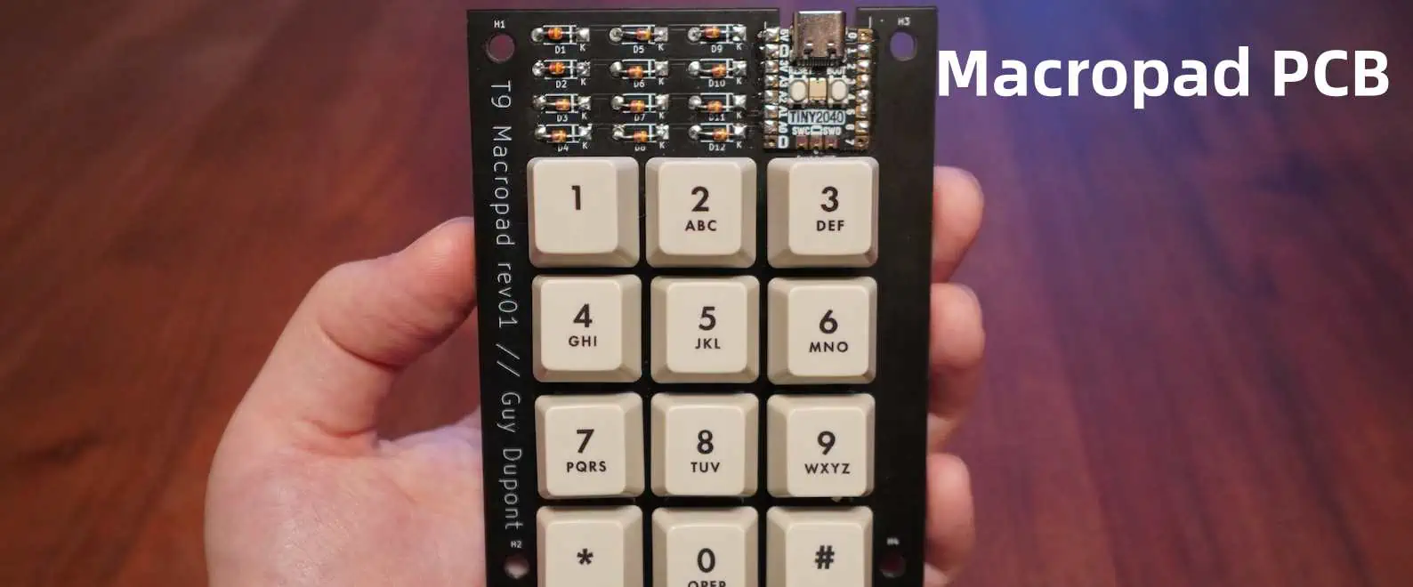
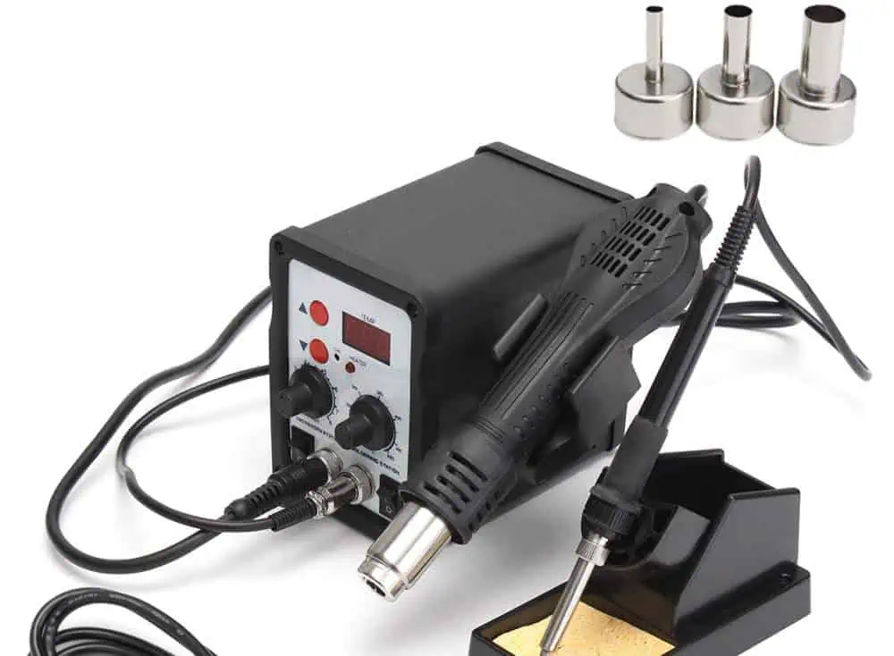
The POC type of prototype is one of the most common types of hardware prototype development that different producers rely on these days. These prototypes are more important when you are aiming for something that needs to be tangible and easier to execute. You can use different off-the-shelf methods, but using Arduino and Raspberry Pi are some common techniques.

When it comes to Arduino for the POC prototypes, we get to know that it renders more features for making these prototypes a successful attempt. It can easily adjust to your requirements for hardware prototype development through its remarkable features and functions. Therefore, there is no doubt that such software is crucial for the development of intense and complex hardware prototypes.

Other than this, producers find it easier to work with 3D laser printing and laser cutting. Different types of industrial-grade enclosures come in handy for the fine completion of this procedure. However, experts believe that it is not a good idea to complicate procedural stages at this stage because it can mess up the designs and final products later.ย 

2.ย ย ย  โ€œWorks-Likeโ€ or Functional Hardware prototype development

Another type that is common here is functional prototypes. These prototypes are different because they are flexible in nature as compared to others, and experts believe that they are more efficient as well. Different sensors and shields are there in these prototypes that give them different functional attributes on all counts.

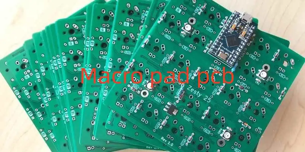
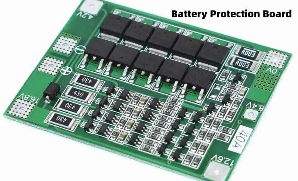
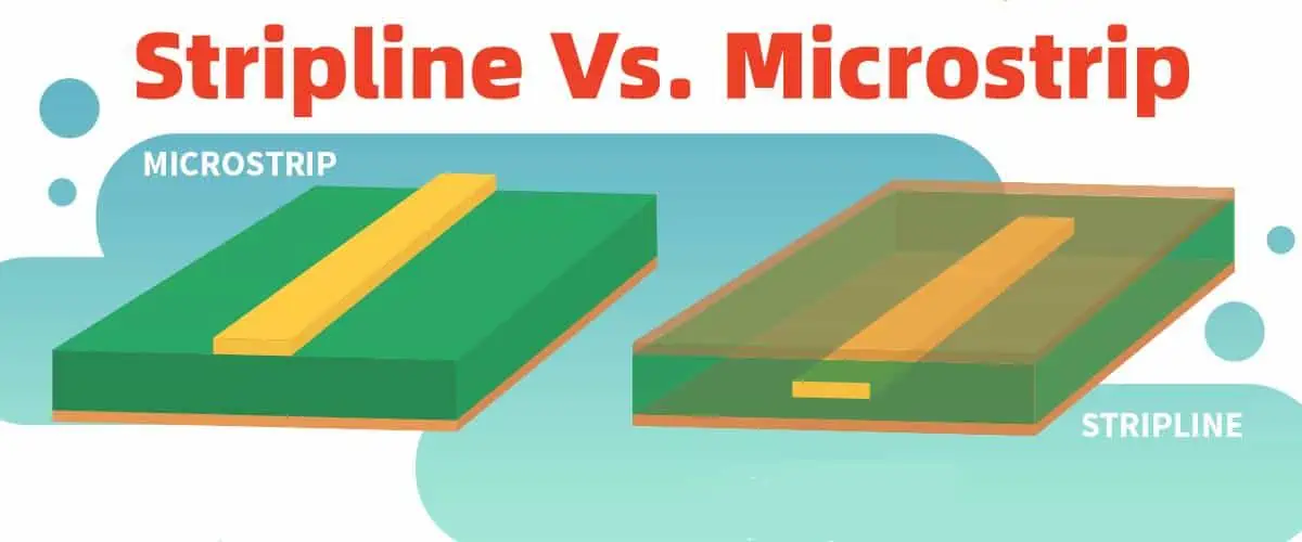
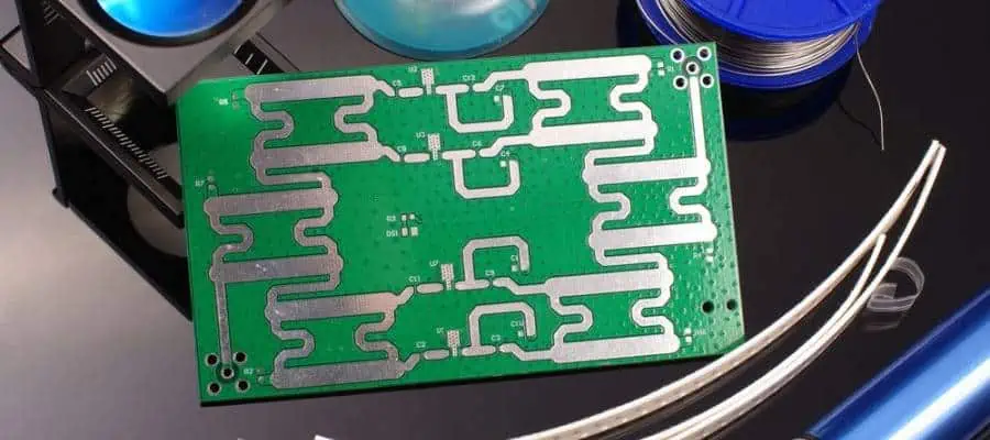
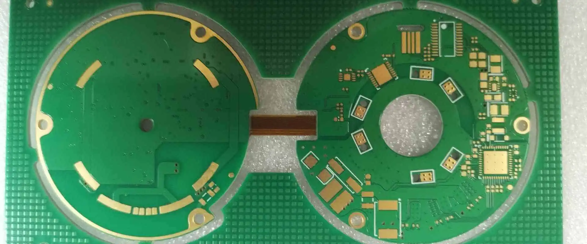
Such prototypes allow you to have a higher degree of customization as well. It is amazing because other prototypes never or cannot allow this to the users. It also implies custom PCBs. In this process, you never rely on redundant components and always try to exclude irrelevant components during the hardware prototype development. Therefore it also comes in handy for the proper utilization of the internal space.

You can use these prototypes to bring your ideas of electronics into reality. Plus, these are somewhat more affordable than other prototypes as well. It is also important to know that when it comes to availing the benefits of functional prototypes, then, you need to seek professional help from product development agencies to ensure desired results.ย 

3.ย ย ย  ‘Looks-Like’ Hardware prototype development

These prototypes are also crucial to learn about when you are aiming for prototype hardware development. Now, what makes them different is that they are totally not functional. However, these look like final products and are thus called โ€œlooks-likeโ€ prototypes.

Well, this name makes it easier for us to understand them and distinguish them from the rest. Such prototypes are mostly common in the areas of industrial design where products need to emphasize more on the end design for consumer electronics.ย 

4.ย ย ย  Alpha Prototypeย 

You can also call them engineering prototypes. Another important category to know about when you are studying hardware prototype development. Well, these prototypes are a combination of works-like and looks-like prototypes.

So now you know how you can avail advantages of two types of prototypes in a single one! Such prototypes are crucial when it comes to crowdfunding and Kickstarter. One important point about these prototypes is the customized PCBs. You need specific containers and enclosures to work on these PCBs so that you can make desired amendments regarding these. You must change the aesthetics, small details, and shape if needed during the process.

After all the changes made, it is important to combine the prototypes with the designs made and see if the designs fully match the prototypes or not. You will also find different producers that use the latest techs, like 3D printing and CNC machining, to give an edge to alpha prototypes under the concept of hardware prototype development. Now donโ€™t think that after all this, you will be able to get the desired results because every alpha prototype needs to undergo injection molding, which is a process that takes place on a much larger scale.

Due to this reason, producers who rely on Kickstarter mostly face disappointment because the process is overall time-consuming and demands more investment. The molding itself is a hectic procedure, and you need to develop the molds as per DFM standards.ย 

5.ย ย ย  Beta Hardware prototype development

After alpha prototypes, we have beta prototypes. Now there are some similarities between these two types. One is that both alpha and beta prototypes appear alike, and they are also common in their functions.

However, one big difference that sets these prototypes apart is the element of DFM optimization which always includes large-scale and high-end manufacturing processes. Take silicone molding, for example. You can consider it similar to injection molding, but it helps you with the production of almost 50 units in a single go. The enclosures used for this molding are specific and industrial grade.

The workers also pay close attention to the plastic components so that the simulations won’t create a negative influence on these fragile components during the process. You can also not forget about the technical analysis, thermal simulations, tolerance analysis, along with structural amendments.

Every producer relies on beta prototypes as per different certifications like FCC, RoHS, and CE. Critical and intense testing methods make these prototypes safe and reliable for fine performance under stressful conditions.ย 

6.ย ย ย  Pre-Production Hardware prototype development

Pre-production is a crucial stage in the process of hardware prototype development. At this point in the process, you can easily make copies of the end designs and components that you desire. You can even escalate this copy manufacturing as per your queued orders.

You need to cut small pieces of steel molds, and this is where you cannot make any further changes. The designs remain intact, and everything that you have changed proceeds further with the process. At this stage, the workers make sure that the prototype and the designs are impeccable.

So that the final product can meet the clientโ€™s requirements. If everything is in place, you call it a โ€œgolden sample,โ€ which showcases 100% quality of the product. The producers often separate some samples for PVT purposes as well. When you see that there is no need to make further changes, then it is important to work on the product packaging too.ย 

Best Tools to Build Hardware prototype development

FULL PCB MANUFACTURING Quote

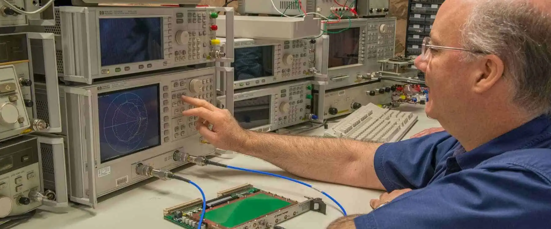
The field of hardware prototype development has undergone different upgrades, and the tools that we use for it are also changing. So the latest tools that we use for this purpose are important. A smart prototype product or provider will make sure to rely on these tools to enhance the results and meet the clientโ€™s expectations and requirements completely.ย 

1) Arduino

One of the most common and appreciated prototyping tools is ARDUINO. It is an open-source platform to make your prototype development more fun and easier. You can use it for both hardware and software development both. You can make changes to its circuit board as per your needs. Besides, its IDE is also supportive of different computer species.

Coding with Arduino is a lot simpler, and different prompts make your coding faster as well. You can use Arduino for different purposes, and each time, you get desired results from it. Therefore for different users who are into hardware prototype development, there is nothing that can compete with Arduino on all counts. From basic AI tools to complex robots, Arduino can handle all your prototyping complications.ย 

2) Raspberry Pi

The Raspberry Pi is, however, an affordable alternative to Arduino. It is portable hardware, and you can use it by connecting it to your personal laptop or PC. No matter what is your computing level, you can use this thing easily. Even beginners find using Raspberry Pi fun and a lot easier during their computing journeys.

You can just consider it a mini PC, and it can serve internet browsing, using spreadsheets, computational processing, and much more. Want to play games with Raspberry Pi? It is possible! Today different organizations are using this portable hardware for weather-detecting purposes and combing IR devices like IR cameras for different motives.ย 

3) Off-the-shelf enclosures

Housing is important for the well-being of your electronics. When we are learning about hardware prototype development tools, we need to understand that off-the-shelf enclosures are crucial for this purpose.

You will find different enclosures available for this, but you have to identify your needs for choosing an enclosure. There are also different factors that you can consider while selecting the perfect enclosure for your electronics. There are some providers that will allow you this, and you can avail of this service from them as per their charges as well.ย 

4) 3D CAD softwareย 

If you have never been familiar with 3D CAD software, then it’s high time that you do! Well, CAD proves to be handier when you are considering custom plastic parts and other technical components.

The degree of customization that CAD offers is unmatchable as compared to other prototyping tools. There is no doubt that CAD is a little bit on the expensive side for some producers, but it is all worth it. However, you can still use CADโ€™s free version to obtain different features for the development of impeccable prototypes.ย 

Considerations for Hardware prototype development

There are some salient considerations regarding hardware prototype development that you must consider for procuring desired results. These considerations will help you understand your clientโ€™s expectations, and you will be able to meet their requirements successfully.ย 

You need to know that hardware prototype development cannot be done in a jiffy. Instead, the duration of completion of these prototypes mainly depends on their nature. Simple and basic prototypes can be developed in a few weeks. At the same time, complex prototypes can even take months! However, you can still strike a perfect balance right from the beginning of the prototyping process to get the desired results.

Can you meet the deadlines? What requirements of your clients will take more time to complete? Are you prioritizing completely in terms of prototyping? What type of tools are you investing in, and are they really with it?

All these factors will help you develop a sense of evaluating your options to work your clientโ€™s requirements successfully. For the speed-to-market, you need to know that complex and intense prototypes will reduce it.

For simple and basic prototypes, the speed-to-market is more. Being a brand, you need to pay heed to marketing and new product launches to attract more people to your services. It will help you meet the market demand, and you will be able to secure a firm position in the market at the same time.ย 

Conclusion

There is no doubt that you need to gather all the possible information for hardware prototype development before practically beginning with it. There have been cases when producers had to face severe loss of investment due to ignorance and lack of knowledge.

RayPcb hopes that from this discussion, you can now easily comprehend hardware prototype development and give your production an edge from this day forward.ย 

What are Radio Frequency Waves?

RF Hardware Engineer

Radio Frequency or RF Frequency refers to the type of electromagnetic radiation used mostly in the communications industry. In this blog post, you will learn more about the uses of radio waves, the radio frequency applications and the radio waves frequency range.

How Did Radio Frequency Waves Come About?

The concept of radio frequency can be dated back to the 1870s when a Scottish physicist, James Clerk Maxwell embarked on research called the unified theory of electromagnetism.

Among many things, it proved the following:

  • It predicted the possibility of a coupled magnetic field and electric field to travel as an electromagnetic wave, through space.
  • The theory, now known as Maxwellโ€™s Equation, proposed the possibility of light to comprise short wavelengths of electromagnetic waves.

It is based on the premise of this theory that Heinrich Hertz, a German physicist, in 1887, put Maxwellโ€™s theory to test. The demonstration involved the generation of radio waves in the lab, and the outcome showed that the waves possessed some similar properties as light. These properties include but are not limited to: polarization, standing waves, diffraction and refraction.

What is RF Frequency in the Modern World?

RFT Testing

The experiments by both Maxwell and Heinrich helped lay the framework for what we have today. Now, Radio Frequency (RF), according to Wikipedia, is the โ€œoscillation rate of an alternating electric current or voltage.โ€

It can also be used to describe the following:

  • The oscillation rate of a mechanical system in a frequency.
  • The oscillation rate of a magnetic.
  • The oscillation rate of an electromagnetic field.

Going by these definitions, the radio waves wavelength, in addition to being the longest, typically range between 20 kHz and 300 GHz. The usage in Radio Frequency (RF) technologies and or applications is due to the frequencies from where the energy coming from an oscillating current are radiated off into the space, in the form of radio waves.

Contrasting between RF Frequency and Radio Waves

A slight difference exists between Radio Frequency (RF) and radio waves, even though they are sometimes regarded as one.

Here are some of the differences:

  • The wavelength in radio waves is inversely proportion to the radio frequency.
  • Charged particles, which have been accelerated, lead to the radiation of radio waves, while the electric currents that oscillate at Radio Frequencies (RF) do not have the properties shared by lower audio frequency alternating current or direct current.

Radio Wavesโ€™ Generation

The waves are generated in a wide range of ways, including via a time-varying electric currents, and radio noise produced by lighting and other forms of naturalized processes.

The simplest explanation is that radio waves are generated by a transmitter and a receiver detects it. The next processes include the passage of the radio transmitter through the antenna. This enables the transmitter to send energy into space and for the receiver to receive or pick up the sent energy from the space.

The Types of Radio Waves

Different kinds of radio waves exist and choosing the one to work with depends on the typical applications.

Here are some quick facts about the types of radio waves:

  • They are labelled or categorized into bands or ranges, such as: Low Frequency (LF), Medium Frequency (MF) and High Frequency (HF).
  • Each of the ranges or bands tend to have an increase of frequency that corresponds to the power of 10 (or the order of magnitude).

With that being said, here are some of the options:

a.    Low-to-Medium Frequencies

These are the lowest in the โ€œwaves chain.โ€ Out of these, the Extremely Low Frequency (ELF) stands out. It refers to the radio wave with less than 3kHz of frequency and up to 100 km of radio waves wavelength.

The benefits of the ELF include:

  • These waves are naturally-generated, usually through lightning.
  • The waves can be used for a variety of purposes, including entering rocks and water for an onward communication with caves, submarines and mines.
  • Extremely Low Frequencies (ELFs) are relied on due to the longer ranges.

On the flipside, you may want to distance yourself from using the ELF due to these reasons:

  • The waves can โ€œbounce back and forthโ€ between the ionosphere and the earth.
  • The disturbances created by the lightning tend to disrupt the transmission of radio signals.

The Low Frequency (LW) and Medium Frequency (MF) ranges tend to incorporate both aviation and marine radio. They also support the Amplitude Modulation (AM) radio, typically the one that falls between 535 kHz and 1.7 MHz

One of the selling points of the Amplitude Modulation (AM) is the long-range, especially at night. On the downside, the long-range is often susceptible to interferences that tend to negatively affect the sound quality.

b.    Higher Frequency Ranges

These are the radio waves with a higher frequency range. They often use a power of 10 or the order of magnitude.

Examples of the radiofrequency waves that fall into the higher frequency ranges are:

  • Very High Frequency (VHF)
  • Ultra High Frequency (UHF) and;
  • High Frequency (HF)

These ranges or bands often use Frequency Modulation (FM) bands for the communications. The benefits of FM over AM include:

  • The radio frequencies are anywhere between 88 MHz and 108 MHz.
  • Frequency Modulation (FM) bands are not often constrained by the ecological components, which is the reason why they hardly experience lower signal quality.

c.    Highest Frequency Ranges

As the name suggests, these are the radio waves with the highest frequency ranges. Some of the attributes include:

  • These ranges are often regarded as a feature of the microwave band and;
  • They are the most-elevated frequencies in the radio band.

The Super High Frequency (SHF) and the Extremely High Frequency (EHF) are the most-prioritized here.

SHF vs. EHF

Despite being the most-elevated of frequencies in the radio band, the SHF and the EHF also differ. For example, the SHF is commonly used for applications requiring shorter ranges of connections. Examples are Universal Serial Bus (USB), Wi-Fi and Bluetooth.

The Super High Frequency (SHF) is preferred over the Extremely High Frequency (EHF), due to the less susceptibility to damage or interference by air.

Generally, the highest frequencies, such as EHF and SHF have shorter wavelengths that support the direction of signals to satellite dish antennas.

However, one challenge with these frequency ranges is the assimilation or absorption of the frequencies by the molecules in the air. This is one of the reasons why these frequency ranges donโ€™t always go beyond certain applications and ranges.

d.    Short Radio Waves

These refer to the radio frequency (RF) waves that use the frequencies in the High Frequency (HF) band. These frequencies range anywhere from 1.7 MHz and 30 MHz.

Attributes of the short radio waves include:

  • Bouncing off of the signals from the ionosphere and the rebounding of the same hundreds of miles from the origin.
  • Short radio waves can also be isolated into different fragments and segments and used for dedicated telecommunication stations, such as Voice of Russia and the Voice of America.

Radio Frequency Applications

Several frequencies of radio waves are used for different purposes, but the common ones are mobile phones, transmitters, computers, televisions and receivers. These frequencies, depending on the ranges, can also be used in the following applications:

  • Remote-controlled toys
  • Control circuits
  • Wireless computer networks
  • Ham radios
  • Military communication devices and;
  • Telephones

The applications of radio frequency waves wouldnโ€™t be completed, without highlighting some of the industries benefiting from it. Examples are:

  • Wireless Devices: examples are Bluetooth, Cellphones, Wi-Fi, television broadcast stations and satellite communication systems.
  • Medical Applications/Devices: radio frequency waves are also relevant in the medical industry. In this case, they are used either in the forms of electrical currents or radio waves (electromagnetic waves).

Today, the usages of radio frequency for medical applications have transcended the above and now include:

  • The use of radio frequency fields in Magnetic Resonance Imaging (MRI). This aids in the generation of the images of the human body.
  • Diathermy
  • Electrosurgery scalpels, which are used for cutting and cauterizing, during laboratory operations.
  • Cancer treatment and;
  • Hyperthermy

Radio Waves Uses

Radio frequency waves are commonly used in the medical and communications industries. However, the use cases are much more than those.

Today, you can find these ranges of frequencies applied to different places. For example, they are now used standardizing the communications via radios and TVs, as well as enabling remote-controlled toys.

Worthy of mentioning is that the RF field usages in the several types of wireless communications is enhanced by the use of transmitters and antennas.

Beyond wireless communication applications, Radio Frequency (RF) fields have now been used in the following:

  • Garage door openers
  • Microwave ovens and;
  • Wireless devices, such as computer mice, TV remote controls and computer keyboards.

Conclusion

The use of Radio Frequency (RF) waves aids in the electromagnetic radiation that has been useful in different key industries. From enabling wireless communications to boosting communications in the home and office, the use of RF waves goes a long way.

Of course, the capabilities tend to differ by the frequency ranges. For the best results, choose from the higher frequency ranges and the highest frequency ranges.

A Comprehensive Comparison of Stripline Vs. Microstrip

Stripline Vs. Microstrip

In Printed circuit Boards, traces are generally given two names depending on their placement in the stack of a PCB; Microstrip and Stripline. In a circuit board, both microstrip and stripline offer two distinct structures of line used in the layout of a PCB. Both strip lines and microstrips come in differential varieties and coplanar. Each of them gives off specific types of benefits while using high-frequency and high-speed signals. This article helps you understand the difference between strip lines and microstrips and guides you through the different benefits and routing styles each of them incorporates. 

However, before getting into the details, it is crucial to understand the basic factor that makes both strip lines and microstrips differ from each other. For the strip lines located inside the stack of a PCB, the traces are fully disclosed to the material of the dielectric. At the same time, the properties of dielectric material will have a better impact on the propagating signal along the strip lines. Read along; you will get to know what factors cause differences between both types of traces.

What Is A Stripline?

Edge-Coupled Stripline (symmetrical) pcb impedance control

A stripline lies inside the material substrate with around two planes (ground) sandwiching the substrate and stripline. This impregnation depicts that the transmission lines can only be available in the internal routing layers of a PCB. Thus, strip lines are mostly found in multilayered printed circuit boards. Also, the structure protects the stripline, reducing emissions.

What Is A Microstrip?

A microstrip refers to a planar communicating line that lies outside the material of the dielectric. The material of the PCB insulates and splits the tace signal from the ground plane. This means that the transmission line possesses air over it. Hence, the transmission line can only lie over the lower and upper PCB layers. Moreover, the air constant of the dielectric and the material of the board affect the impedance of the trace.

Differences: Stripline Vs. Microstrip

However, it’s hard to directly say which routing style suits you better or perfectly. Therefore, the difference helps you determine to choose the right one for your application. So, letโ€™s discuss different areas that depict differences. 

Location

As discussed above, the main difference between both strip lines and microstrips is their placement or location. Striplines lie inside the internal layers, particularly between two ground planes, whereas microstrips lie on the outer layers of a PCB. 

Usage

Typically, you can select between whether to go with microstrips or stripline while routing the designs. Though, you need to consider some things before selecting between any routing styles.

  1. Choose a stripline routing style if you are looking for high-density tolerance impedance for your application. A stripline possesses greater density for impedance-controlled routing as compared to a microstrip. Thus, a thin and small stripline will offer the same value of impedance as a wider and bigger microstrip gives.
  2. Whereas you donโ€™t have to choose any routing method if your circuit board contains short traces between close electronic components. However, you can still choose microstrips only if you need impedance control in your application. 
  3. Furthermore, strip lines do not go well with ultra-high frequencies. Unfortunately, the Via integrating with the internal layer will behave like a distinct transmission line. This allows the surrounding parasitic capacitance to develop impedance continuity and signal losses. 
  4. You can go for strip lines also if you want greater isolation between the layers of your design. This stripline routing style develops isolation in the internal layer, which seems impossible with microstrips. At the same time, this style of design doesn’t guarantee greater isolation between straplines of the same layer. Hence, you have to consider crosstalk before moving forward with the design.
  5. Last but not least, you can use both routing methods with high pin-count electrical components.

Characteristics Impedance

The characteristic impedance of the strip lines relies on the dielectric constant, the center conductor of the strip, and the cross-sectional geometry of ground planes. Furthermore, the characteristic impedance of the stripline decreases when the width of the strip increases. Whereas on the contrary, the characteristic impedance of the microstrip changes with increasing frequency.

Stripline Vs. Microstrip: Transmission Line

The calculation of routing requires parameters like the dielectric constant used in the dielectric layer of the PCB.

Microstrip 

The microstrip routing on the upper and lower level of the circuit board reduces dielectric losses greater than stripline routing. This occurs because of negligible losses of air. Moreover, in microstrip routing, the conductor strip lies at the outside layer, which makes the fabrication process simple.

Whereas microstrip radiates greater energy because of air exposure. However, the constant of dielectric inside the layers of PCB is generally 1.4, whereas 1 for air. These variations determine the difference in impedance value between microstrips and strip lines.

Striplines

On the contrary, the stripline routing method has the benefit of sandwiching the traces of signals between planes (reference). This structure allows the manufacturing of narrower transmission lines over the same values of impedance needed for microstrip routing. Furthermore, the sandwich structure makes better insulation with the material of dielectric. Thus, allowing you to compress the trace routing.

Advantages and Drawbacks of Stripline Vs. Microstrip

Stripline PCB
Stripline PCB

Both microstrip and stripline offer their own types of benefits. Let’s see a glimpse of the pros of each routing style.

Stripline Benefits

  1. Striplines can protect and shield traces of signals from unknown invasive frequencies.
  2. The performance of this routing method will enhance up to 50MHz.
  3. Moreover, strip lines also offer low impedance, which leads to minimum crosstalk and emissions.
  4. Furthermore, this certain routing method also offers greater EMI characteristics.

Microstrip Benefits

  1. Microstrips contain open transmission line structures which make connections between the electrical components and the surface of the PCB easily. 
  2. Moreover, you can also stack up microstrips on HD channels with lesser crosstalk. This makes it the perfect design for microwave IC and RF.
  3. Microstrips contain planar topology, which gives them a little immunity to circuit board fabrication tolerances.
  4. Furthermore, they also offer faster times of propagation.
  5. Last but not least, this routing method offers mechanical support and heat sinking simultaneously.

Cons

Similarly, each method of PCB routing does have disadvantages too. Let’s dive into the details to know more about them.

Stripline Drawbacks

Tough microstrips come in compact sizes and less price, but they seem loosier as compared to strip lines, waveguides, CPW, and coaxial lines.

Microstrip Drawbacks

  1. Striplines have implanted signal traces which makes them complex to debug. Generally speaking, it makes the prototyping and troubleshooting of the PCB more difficult. 
  2. Striplines can not decouple easily.
  3. Moreover, proper matching leads to low impedance.

Which One Should You Select? Stripline Vs. Microstrip

FULL PCB MANUFACTURING Quote

Each transmission line of a PCB comes with its own advantages and disadvantages. Most PCBs with high frequency and high-speed needs high-density circuits. Therefore, you may end up using both of them in your application. 

Modern printed circuit board tools aid in simplifying the routing configuration of stripline and microstrip. Moreover, the impedance calculators for PCBs also greatly help in determining the perfect layer configuration and width of the trace. Whereas the stack-up editors also facilitate using the right material and width of the board. 

The combination of these tools aids you in choosing the best microstrip and stripline routing approach and configuration of layers with the routing layers.

Conclusion

Both microstrips and strip lines possess a slight structural distinction that changes their nature and properties greatly. However, every transmission line has certain properties that may tend you to use both in your high-speed and high-frequency circuit board to reduce losses. RayPcb hopes this clears all your doubts, yet if you still have any queries, then reach out to us.

What do you Need to Know about Trace PCB?

pcb trace antenna

Trace PCB mainly refers to a network of wiring and insulation made with copper. Typically, if the electronic device starts acting up or damaging, then there is a high chance that the PCB trace is not compatible with the device. Moreover, trace resistance is considered one of the most common terms that electronic engineers often use in the industry. However, this trace resistance specifically refers to those parts of the PCB that oppose the current flow.

What Is Trace PCB?

PCB trace plays as important a role as a current plays in a PCB. Moreover, it requires much time and effort to evaluate or detect the errors in the traces. And if you ignore this error, this may lead to damage to electronic devices. A Circuit board consists of various types of electrical components. Therefore, you should know which type of material and part you will require for assembly or repairing the PCB. Not only this, you also need to know the advanced methods and applications that help in the fabrication process of a PCB.

Width of Trace PCB

PCB trace width is considered one of the most crucial aspects in the layout and design of a PCB. It is very important to carry out the current through the board while maintaining the temperature of the trace below a certain limit to avoid overheating.

Traces operate to transfer signals from and to the soldered component pins on the PCB. They carry different amounts of current based on the network. The trace signals have specific current requirements which affect their size. However, trace width needs to be regulated carefully for efficient and accurate manufacturing of a PCB.

Traces typically consist of a metal connection made up of copper while the etching process of a PCB. The process of etching is considered complex. Therefore, it demands extra care from the fabricators to ensure that traces are not over-etched. This results in thinner and required trace-width manufacturing. 

Moreover, when traces remain isolated over the board surface, then they become more etched than the clustered and grouped traces. This happens due to the etching concentration on a specific area. However, to avoid this, make sure to widen the isolated traces a little. This prevents them from exceeding the required etching. Moreover, excessively etched traces enhance the chances of impairing the PCBโ€™s signal integrity. Therefore, it is necessary to make sure that the PCB trace must meet the required widths. 

The current of Trace PCB

The capacity of PCB trace current is the max current limit that flows through the PCB trace without damaging any electrical parts of the board. Moreover, the PCB trace current depends on the thickness and width of the trace.

Tips For Better Designing of Trace PCB

Creating a perfect PCB trace layout is complex, which impacts the overall functionality, performance, and durability of a PCB. However, we list some tips that help you design better PCB traces.

1.    Routing 

Routing of a PCB consists of two types, automatic wiring and manual wiring. The automatic wiring operates on design software which plays a vital role in PCB design. PCB trace designers cannot rely solely on this feature. On the other hand, manual wiring plays a vital role in the creativity and flexibility of the fabrication process. Moreover, automatic wiring consider is one of the time-saving options.

2.    Width Of Trace PCB

The trace width of a PCB plays an essential role in the overall functionality of a PCB. However, it is very crucial to determine that the trace width of a PCB must have the ability to bear capacitance. Not only this, it must ensure that the width of the PCB must allow a smooth current flow. Moreover, try to determine a precise and accurate size of the minimum width of the trace, as it aids the PCB from overheating. Since overheating directly affects the performance of the board.

3.    Connecting To The Ground Plane

It is crucial to connect traces with the ground instead of separate ground joints to ensure the consistent measurement of voltage across each trace of a PCB. However, the ground plane acts as a shared reference point serving all traces. This prevents variations in resistance and voltage. Therefore develop a rigid ground plane under the path of signal-carrying because it reduces the impedance and increases resistance to sound. Moreover, placing ground and power planes in the internal layer of a PCB can prevent electronic component separation or distortion.

4.    Minimizing Capacitive Coupling

The ground planes and the adjacent tracks of the PCB creates capacitive coupling. However, make sure to separate the traces of PCB that are devoted to the analog signals and power supply. It helps in reducing the effect of capacitive coupling between the upper part of traces and the lower parts of ground planes. Moreover, decoupling capacitors acts as one of the most affordable and efficient ways to copy the capacitive coupling within the layout of a PCB.

5.    Separating High-Speed and Low-Speed Signals

Try to keep low-speed and high-speed trace signals separate from each other, as it helps in reducing interference and crosstalk. However, you can easily achieve this. Just try to use ground planes as a means of isolation hurdles and route traces over each layer. This way, you can easily separate both high and low-speed trace signals from each other.

How To Fix Trace PCB?

FULL PCB MANUFACTURING Quote

The knowledge of manufacturing PCB trace and its basic principles is not enough; you must know how to repair them too. However, whenever the unit power supply starts malfunctioning, like unusual noise or display failure, at that time, traces of the PCB surely need repairing. Therefore, we have some steps here which give you a detailed insight into the repairing process of a PCB trace.

  1. Firstly, look for damaged traces over the PCB surface.
  2. Once you find the damaged trace, then use a cutter to take it out from the board. Ensure that the cutter does not touch or damage the nearby electrical components. 
  3. After that, clean the surface of the board firmly until the board shows its real color of copper. Then apply solder over the exposed area. 
  4. After applying the solder, clean the area again with the help of a solvent pen cleaner or paper towel. Put the flux over the damaged area. Then solder the tracks back using a soldering iron.
  5. Then select a substitute wire that fits perfectly with its size.
  6. Tin both tips of substitute wire.
  7. However, if the substitute wire fits perfectly with the board, then it does not need any insulation on any side. Remove it from both sides. Then solder the wire to its required location firmly.
  8. First of all, solder one side while ensuring that the substitute wire overlaps the available trace by a minimum of two times the PCB trace width.
  9. After that, you shape and mold the wire depending on certain requirements and needs.
  10. Use adhesive or tape to firmly attach the substitute wire to the PCB’s surface.
  11. Then solder another end of the substitute wire.
  12. In the end, make sure all the connections work perfectly and there is no error behind them. Clean the area one last time to remove any remnants of stains or residue.

Conclusion

The best trace routing of PCB determines the durability, functionality, performance, and cost of the PCB and electronic device. Trace routing not only enhances the productivity of PCB but also makes the manufacturing process easier. Therefore, it is very crucial to learn and understand the mechanism of PCB traces and trace routing. Therefore, if your queries are still unanswered, you can contact us anytime. We will surely help you clarify your queries in the meantime.

Comparison between Desoldering Wick vs. Pump

Desoldering Wick vs. Pump

It is very important to have adequate tools by your side when you are dealing with desoldering. Desoldering Pump and Desoldering Wick are considered two of the most popular ways to eradicate solder from components of a PCB. However, both tools perform the same function of eradicating the solder. But they give different benefits.

The difference between a desoldering pump and a desoldering wick helps you choose an appropriate desoldering tool. It does not matter whether you prefer efficiency, cost, precision, or cleanliness; this article will give a detailed insight into the features, working principles, and benefits of both desoldering tools. Thus, helping you in choosing the best tool for your desoldering process.

Desoldering Wick

Desoldering Wick
Desoldering Wick

How Does Desoldering Wick Work?

Desoldering wick is also termed a soldering braid or solder wick. It refers to a braided flat copper cable with a flux coating. It absorbs molten solder as the heated soldering iron is put on it. Thus making you able to eradicate the slider efficiently.

When Should We Use A Desoldering Wick?

Desoldering pumps or soldering suckers act as vacuum cleaners, while desoldering wicks act as mops. However, the ability to desolder the wick of solder absorption makes it crucial in applications and devices which do not accept solder splatter.

Furthermore, it naturally encourages desoldering wick better at removing off slider from SMT pads along with removing solder gaps on fine pitch BGA and SMT pads found on SMD integrated components PCBs. Though SMD components use special desoldering tweezers or rework stations of hot air to desolder, the desoldering wick also comes in handy. 

Whereas a desoldering pump cannot be considered useful for any type of SMD component rework. It happens because of the too-flat conductive pads of PCB, which cannot absorb the solder efficiently. It’s more like drinking soup from a plate with a straw.

Nonetheless, desoldering pumps serve better in desoldering PTH joints. Though a desoldering wick may also do this, capillary action does not have enough efficiency in absorbing a larger quantity of molten solder from an in-depth cavity of a plated through-hole joint. The additional copper braid thermal mass and bigger PTH joint enhance the dwell time. This, however, is risky for both copper trace and electrical components on the Printed Circuit Board.

Selecting A Right Desoldering Wick 

Desoldering wicks generally come in 5ft and 10 ft spools, which are also known as bobbins. Bigger spoons come in between the range of 500 ft to 25 ft, but such a large quantity doesn’t suit hobbyists much. Length gives convenience, but choosing a wick with the right width is a very crucial factor to consider.

YouTube video

ยท       Braid Width

Desoldering wicks come in a variety of width options ranging from 0.8 mm to 5 mm. However, according to the thumb rule, the width of the braid must either be exactly equal to the size of the pad or a little larger. Small-size braids will not have the ability to remove the solder from the whole pad, while oversized wicks will impact the nearby pads that you don’t want to desolder. 

Moreover, braids with smaller widths also tend the users of the wick to move and take them around during desoldering. This, however, enhances the chances of delaminating the pads from the circuit board. Moreover, an excessively wider desoldering wick also enhances the thermal mass of the components and increases the dwell time on electrical components. Once again, this enhances the chances of Printed Circuit Board pads and electrical components damage. 

ยท       Soldering Tip Size

The same reasoning also becomes valid for the tip of the soldering iron. It must match the width of the braid ideally. If the soldering iron has too small a tip, it heats the iron slowly, which enhances the dwell time with the chances of electrical components damaging. Whereas on the contrary, oversized tips of the soldering iron can affect nearby electrical components.

Hoof tips, knives, and chisels fit best for this type of job. Moreover, make sure to avoid utilizing the conical tips of the soldering iron as they have small patch contacts which guide to poor and bad thermal connection.

ยท       Flux Composition

Last but not least, the composition of flux also plays a vital role in the whole desoldering wick. If the workflow demands no-clean solder usage just because you don’t want to clean, then you must utilize a type of desoldering wick with no-clean flux infusion. Whereas, if you wish to clean the Printed Circuit Board Assembly post-type rework, then use rosin flux as they have the fastest wicking action.

Moreover, desoldering wick also comes in the form of no additional flux specifically designed for certain rework processes. Thus, this enables you to utilize your flux which hobbyists usually use to prevent the chances of contamination.

Instructions to Use A Desoldering Wick

Desoldering wick offers a simple process of using it. Here are some steps that help you understand how to use desoldering wicks efficiently. 

ยท       Preparing Your Tools

Gather all the necessary equipment and tools like desoldering wick, solder flux, and soldering iron.

ยท       Heating The Soldering Iron

Plug in the soldering iron. Set the temperature and leave it to heat up. The standard temperature relies on the solder type used in the process; therefore, refer to the recommendations of the manufacturer of the solder.

ยท       Positioning The Desoldering Wick

Put a desoldering wick in the place of a solder joint that needs to be removed. However, make sure that a wick entirely wraps the solder.

ยท       Applying Heat

Place the soldering iron head or tip over the desoldering wick right where it makes a connection with a solder joint. Now apply a very gentle force to ensure firm contact.

ยท       Melting The Solder

Heat the joint using a soldering iron which allows the solder to be liquidy and flow over the desoldering wick.t The cooler strands of the wick will later absorb the solder.

ยท       Moving the Wick

Once the solder fully melts down, carefully shift a desoldering wick through the joint while following the molten solder flow. This, however, enables the desoldering wick to absorb solder as much as it can.

ยท       Removing The Wick

Once the desoldering wick absorbs the solder, take off the desoldering wick from a joint. Try to remove the wick carefully as solder, and the wick can still be very hot. 

ยท       Inspecting The Joint

Once you remove the wick from a joint, inspect the solder joint to make sure that the molten solder has been appropriately removed. However, if necessary, again, repeat the whole process by desoldering the wick’s new section.

ยท       Cleaning The Tip

Clean the soldering iron tip with the help of a brass cable cleaner or damp sponge to keep its efficiency. This process, however, helps in removing any type of solder flux or residual solder.

Inspecting The Desoldering Wick

Fully examine the wick for signs of clogging or saturation. If the wick loses its ability to absorb or becomes saturated with molten solder, then replace the wick with a new one. 

However, always be cautious while working with a soldering iron as it might be very hot to prevent damage or burns to components. Handle all safety measures and use tools with all care.

Desoldering Pump

How does It work?

Desoldering pumps are also termed solder extractors or solder suckers which use a spring-loaded function to make suction. On triggering the pump, it quickly sucks away the solder from a joint which makes the removal easier.

How To Use A Desoldering Pump?

Desoldering pump refers to a type of portable machine that offers outstanding services like removing molten solder from the surface of a PCB. It, however, helps in removing the solder after heating it. Here are some steps that help you understand the procedure for using a desoldering pump.

Instructions To Use A Desoldering Pump

  1. First, apply heat to the molten solder using the soldering iron. However, in some scenarios, the desoldering pump can also come with the soldering iron.
  2. Second, press the plunger down and apply adequate pressure over it. However, in the case of desoldering pumps that have bulbs, you may squash them.
  3. Third, after liquifying the solder, place the pump head over the removing molten solder.
  4. Then comes the discharge or release of the bulb or plunger. Some specific desoldering pumps come with a special design that contains a button for release. 
  5. After that, remove the required free electrical component. 
  6. Repeat the process to fully remove any extra solder from the board.

First, press and then release the bulb or plunger constantly to remove the molten solder within a desoldering pump. The bigger clumps of molten solder have a tendency to remain in the form of liquid for a greater period of time which makes it easy to discard. However, whenever you try to remove extra solder, make sure to add additional solder on the joints.

Here are some specific benefits and drawbacks that both desoldering wick and desoldering pump offers.

Advantages Of Desoldering Wick

ยท       Precision 

Desoldering wick provides better accuracy in terms of removing tiny solder balls or dealing with sensitive electrical components. The flexible and thin aspect of a wick enables you to approach specific areas on the board with greater precision.

ยท       Ease Of Use

Desoldering wick allows easy access and easy usage, which makes it easy for beginners to use it. Just simply put the wick over the solder joint, then apply heat on it using a soldering iron tip. Leave it for a few seconds to let the wick suck in the molten solder. 

ยท       Cost-Effective

Desoldering wick serves as more affordable and cost-effective than desoldering pumps as it allows you to use them multiple times, which makes it a reasonable and budget-friendly choice for regular desoldering activities. 

ยท       Accessibility

Desoldering wick comes in a variety of types and sizes which makes the availability and purchase easy.

Disadvantages Of Desoldering Wick

ยท       Flux Consideration

Desoldering wicks already come with a coating of flux on it which allows the absorption of solder. But the flux may lose its efficiency or dry out with time; therefore, you may need to add extra flux for better results.

ยท       Slower Desoldering

Desoldering wick consumes greater time in removing various soldiers than desoldering pumps, particularly for comprehensive desoldering activities.

Advantages Of Desoldering Pump

ยท       Efficiency

Desoldering pumps serve to remove larger amounts of molten solder quickly. They generally come in handy when working with bigger electrical components or solder joints that need a robust suction force.

ยท       Cleanliness

Desoldering pumps collect the removed molten soldering in a different chamber which helps in keeping the work space cleaner. However, this lessens the risk of molten solder splatter. Also, making the disposal of removed solder waste easy.

ยท       Reduced Heat Exposure

Desoldering pumps enable the soldering joints to expose to a lesser amount of heat than desoldering wicks. However, this proves helpful in dealing with delicate PCBs or heat-sensitive electrical components.

Disadvantages Of Desoldering Pump

ยท       Limited Precision

Desoldering pumps do not provide the same amount of precision level as desoldering wicks do whenever it deals with sensitive components or removes less amount of molten solder.

ยท       Maintenance

Desoldering pumps need occasional maintenance and cleaning to enable optimal performance. Debris or clogs can dramatically impact the action of suction of a pump.

ยท       Cost

Desoldering pumps cost a little higher as compared to desoldering wicks, which may prove helpful for people with tight budgets.

Conclusion

Both Desoldering Pumps and Desoldering Wicks come with their own benefits. Desoldering provides cost-effectiveness, ease of usage, and precision, whereas a desoldering pump offers cleanliness and efficiency and lessens exposure to heat. 

Make sure to consider some important factors like desoldering nature requirements, components involved in the process, and some other factors which help in choosing the best tool. However, for a safe passage, take both the dealing pump and the desoldering wick in the toolkit. As this not only enhances the versatility but also makes you handle a variety of desoldering tasks with ease.

A Beginnerโ€™s Guide to Ordering Custom PCB

Customized rigid flex PCB

Certain electronic projects need specific configurations. If you are using a Printed Circuit Board (PCB) for such projects, there is a likelihood that you would need a customized version. Find out in this article, some of the basic things you need to know about ordering custom PCBs.

What is a Custom PCB?

As the name suggests, it is a โ€œcustomized version/variantโ€ of a Printed Circuit Board (PCB). However, a lot more goes into the development, than just mere configurations.

Here are a few quick points about what a custom PCB offers:

  • Multiple Electronic Component Support: the customized version of circuit boards supports the integration of several electronic components. The integrations range from strips of conductive materials (such as copper), as well as smaller electronic components.
  • Maximum Optimizations: the optimizations and or configurations are extensive. For example, you could use the customized version of circuit boards for integrating several electrical components and other circuits.

Using a customized version of PCBs is a nice way to save space, integrate many components as possible and balance the complexities of the electronic components with the required functions.

Pros of Ordering Custom PCB Boards

Rogers RO4835T PCB

The benefits of ordering custom circuit boards range from having an opportunity to make the boards into whatever needs or uses you may have.

These are some of the additional advantages:

a.    The Circuitry is Condensed

One benefit is that the customized boards have a condensed circuitry. This is due to the space-saving or compact design that allows for many electronic components to be fitted into the smallest of spaces.

b.    Custom PCBs Offer More Technical Options

You and the custom PCB design company are in charge of the entire process and are better-positioned to improve on the boardโ€™s technicalities.

The following are some of the technical benefits:

  • You can choose between multiple design technologies, such as Surface-Mount Technology (SMT) and Through-Hole Technology (THT). More often, the THT process is prioritized for making a custom circuit board, due to the increased parasitic inductance.
  • The technicality also allows for the maximization of even the smallest of real estate/space on the board.
  • You can take advantage of the custom PCB software to manage the circuit boardsโ€™ parasitic inductances/properties.

c.    Longer Serviceable Life

Circuit boards reduce the overall manufacturing costs and can adapt to different sizes. Further customizations can also increase the usability; hence, the reason why custom PCBs have a longer serviceable life.

When compared to the mass-produced boards; they offer a mix of stronger circuitries and careful assembly. Hence, the custom board is less likely to be plagued by poor soldering and loose-hanging wires.

d.    Custom PCBs are Affordable

The affordability of custom circuit boards can be seen in the automated process. With less human and manual inputs, more money is saved from using manpower.

Other cost-saving mechanisms are:

  • Less resources are required, since the boardโ€™s size are subject to further optimization or being made compact.
  • The automated process comes with other benefits, such as increase quality, repeatability and accuracy.

e.    Designing Custom PCBs is a Pathway to Product Originality

Certain electronic products are deemed to be of a higher quality than the others are. This assertion is for a couple of reasons, one of which is the originality of the PCB design.

To ensure the consistency of the designs and related processes, the PCBs can be made to have a similar feature. All you need to do is inform the PCB designer of what you want to achieve and provide the right prototypes assembly pcb. The designer would then go on to replicate the same designs across the different circuit boards.

Here are some of the benefits:

  • Your circuit boards and the electronic products made from the same will have similar operations.
  • Your electronic products will be different from those of your competitors, in the sense that the capacities and performances will be different from what theirs has to offer.

f.     Custom PCBs are Highly-Efficient

Looking for one of the best boards to use for an electronic product design? Go for the customized PCBs. Their efficiency is mainly because of the design from the โ€œground-upโ€ and the optimization for specific applications.

Other benefits of placing an order for custom PCBs include:

  • An overall functionality of the board can be confirmed via the use of the integrated Light-Emitting Diode (LED) lights.
  • There may be no need for decals, as direct printing serves that purpose.

Disadvantages of Ordering Custom PCBs

FULL PCB MANUFACTURING Quote

Sometimes, optimizing a Printed Circuit Board (PCB), in an attempt to make โ€œit yoursโ€ may not be favourable.

It is because of these few reasons:

g.    Changing PCB Design Trends

You will agree that the processes of manufacturing circuit boards have continually changed. In the coming years, additional changes, trends and technological advancements would be prevalent.

Boards that have been customized as per the current technology may not be relevant in some years to come. The few that could be may have become so costly to maintain and to fix any damages.

h.    Troubleshooting Difficulties

That a PCB has been customized doesnโ€™t rule out the need to fix any issues that come up. Thus, troubleshooting is important โ€“ but can be hampered due to the enclosures used to protect the board from the working environment.

Customized circuit boards also have a host of other problems, such as a susceptible damage from higher amperages and a requirement for initial tooling.

How to Order a PCB for Custom Production

We will help you come up with one of the best-designed custom circuit boards. However, it is imperative for you to have some important points in mind before placing you order.

Decide on the Type of Custom PCBs

The option is usually between the single and multilayered boards. The former is mostly favoured due to the duplication of the boards.

Partsโ€™ Sourcing

The PCBs need to have the components sourced or gotten somehow. You either provide them or have the PCB manufacturing company do that.

The common component sourcing options include:

  • Turnkey: this entails allowing the PCB manufacturer to handle the entire component sourcing.
  • Combo: for this, both you and the PCB manufacturer will provide some parts individually for the custom PCB production.
  • Kitted: this exclusively allows the PCB customer/consumer (you) to provide the components needed for the design.

Prototype Potentials

What becomes of your custom PCB when the manufacturer is unable to make more prototypes? This is why you need to be sure the company can make as many units of the board as you want as time goes on.

You should also find out what the manufacturerโ€™s Minimum Order Quantity (MOQ) is. Ideally, you want to aim for smaller quantities for prototypes, until you are sure the boards are in good condition for massive productions.

Number of PCB Components Required

TU 768 PCB
TU 768 PCB

Find out the estimated number of parts (components) required for the boardโ€™s customization. These parts are further classified into the Through-Hole (THT) components and the Surface-Mount (SMT) parts.

RoHS Compliance

The Restriction of Hazardous Substances (RoHS) is required to validate the safety of using your electronic circuit boards in different countries.

The benefits of designing an RoHS-compliant custom PCB include:

  • Making the boards suitable for sales and use in other countries.
  • The compliance also provides a sort of legal coverage for the boards, in the event that a consumer gets injured when using the boards.

Testing Options

A wide range of tests are performed on the custom PCBs. Examples are:

  • X-Ray Test: the X-Ray inspection/test is used for the custom PCB designs that have their leads hidden underneath the components.
  • Functional Test: this is a testing method used to confirm the โ€œfunctionalityโ€ of the circuit board. The following are validated in the process: the absence of open or short circuiting, that the board has excellent solder connections and that the right components are used and are installed in the right places.

Customizations vs. Changes

The customization of a PCB shouldnโ€™t close up all channels of making relevant changes to the board. Can the board be open to further optimizations and or changes? Can further integrations be made, especially when new technologies are released?

The need for changes should be one of the factors to consider. Here are the major considerations:

  • Save some space inside the PCB to allow for the new components to be added.
  • The current design shouldnโ€™t be โ€œstiff,โ€ but done in a way that much-needed changes can be made with ease.

The goal is to customize the PCB with a future-proof approach, which allows for the boardโ€™s design to be changed or adapted accordingly in the future.

Conclusion: How to Design and Order Custom PCB

To design your custom circuit board, use a dedicated software. Once the design is ready, go to the manufacturerโ€™s website and upload it. You will get a quotation based on the submission and on the validation of the process, the customization process will commence.

For the necessary help, contact a professional custom PCB manufacturer. We are committed to helping you source the components, make the boards future-proof and implement the design requirements to the latter.

Your Guide to Choosing a Reliable RF Manufacturer

RF Multiplexer

Choosing a specialist in making Radio Frequency (RF) PCBs could be the key to developing high-performing circuit boards. As the cost-effectiveness and faster operational capabilities of these circuits buoy the demands; it is also good to have a reliable manufacturer at hand.

In this article, you will learn some of the โ€œinsider informationโ€ on how to choose the best RF manufacturers. You will also find out why these boards are better an some of the comparison to regular PCBs.

The Definition of RF PCBs

These are the Printed Circuit Boards (PCBs) designed to operate at higher frequencies. Such an operation is facilitated by the higher signals contained in the components.

Other key points about RF PCBs include:

  • The signals operate in the Megahertz (MHz) to Gigahertz (GHz) frequencies. To this end, the circuits can move from low to high frequencies.
  • It is common to use RF PCBs for applications or electronic products requiring higher operating speeds.
  • The complexity of designing RF PCB is also an issue.

Who Makes the Best RF PCBs?

RF Filters
RF Filters

An RF PCB manufacturer produces these kinds of boards. Their capabilities differ, as well as the types of RF boards they produce.

We present to you, some of the RF semiconductor companies and what they offer.

1.    Millennium Circuits Limited

This company makes a proper engineering and development of Radio Frequency (RF) circuit boards. It primarily focuses on the production of high-frequency PCB laminates.

The companyโ€™s capabilities include but are not limited to designing up to 44 layers of RF PCBs, using controlled impedance and the Via-in-Pad with Fill options.

Millennium Circuits Limited is also capable of:

  • 35:1 drill aspect ratio
  • Sequential Lamination
  • Quick-turn production
  • Up to 24-inch by 30-inch panel size
  • Copper Plug, Conductive and Non-Conductive
  • Blind / Buried Vias and Micro Vias

Specialized RF PCB Production Process

Millennium Circuits Limited uses a combination of specialized equipment and standard processes for designing the RF PCBs.

The following are some of the specialized production processes:

  • Laser Direct Imaging (LDI): this favourably compares to the conventional photo exposure tools due to the front-to-back registration requirements and the tighter trace width.
  • Plasma Etch Machinery: this is used to ensure proper processing and manufacturing of RF PCBs via the minimization of deviance and maintenance of high-quality in the through-holes.

2.    Cirexx International

Cirexx is a US-based RF PCB manufacturer. It is a full-suite electronics solutions company that offers anything from layout, fabrication, assembly and testing of PCBs.

The RF PCBs include ensuring the compliance of the boards to the Design for Manufacturability (DFM), designing and fabricating the boards.

Other capabilities are:

  • Sourcing up to 60 RF PCB materials from different material manufacturers all over the world. Some of these manufacturers are: Ohmega, Isola, Ventec, Dupont, Megtron, Rogers and Arlon. Others are Taconic, Sheldahl, Panasonic, Evonik, Ticer Technologies, Hanwha, Nelco, ThinFlex, and Tatsuta.
  • Using an in-house RF PCB production method. This covers the fabrication of every aspect of the boards inside one factory, without outsourcing.
  • Cirexx also offers quick-turn production, ideally from 24 hours.
  • The availability of tighter route tolerances.
  • Back drilling
  • Optimization of the RF boards for use in these industries: industrial, consumer electronics, automotive, medical and military/aerospace.

3.ย ย ย  RAYPCB

RAYPCB is a Chinese Radio Frequency (RF) PCB manufacturer. It specializes in producing different kinds of these boards, including the multilayer variants.

RF PCB Materials

RAYPCB sources different kinds of RF board materials from several RF component supplier. The types of materials include Modified Epoxy, FR4, Polyimide, PTFE, Ceramic, Cer/PTFE, Special Laminate, PTFE/Glass and Hydrocarbon/Cer.

The companies it sources these materials from are:

  • Isola
  • Bergquist
  • KB
  • Rogers
  • Panasonic
  • Taconic
  • SHENGYI
  • TUC
  • ITEQ
  • Stablcor
  • Nelco
  • Ventec
  • Hitachi
  • Arlon

Different Types of RF PCBs

RAYPCB designs up to five (5) types of RF circuit boards. These are:

  • High-Power RF PCBs: these are multilayered PCBs optimized to use several layers to enable interconnections inside the boards.
  • HDI RF PCBs: these circuit boards use higher densities and are required in HDI display applications, such as audio equipment and high-resolution monitors.
  • Microwave RF PCBs: these circuit boards are used in several microwave-frequency applications, including smart appliances, mobile telecommunications and automotive electronic systems.
  • BGA RF PCBs: these are dedicated to the Ball Grid Arrays (BGAs).
  • Laser Cut RF PCBs: the benefits include faster fabrication and less residue.

Multilayer RF PCB Production

RAYPCB also produces RF PCBs with multiple layers. The options range from double-sided RF boards to the 4-layered, 16-layered, 20-layered and the 30 layers of boards.

Note: the manufacturer also classifies the RF PCBs by the thickness. The options range from 1oz to 6oz copper RF PCBs.

4.    Sunstone Circuits

This RF PCB manufacturer believes in the concept of โ€œspecialization.โ€ This is why it takes the care to make and modify the boards to be unique than what could have been obtained from the traditional circuit board designs.

Sunstone Circuits uses a wide range of materials, such as those sourced from Polyflon, Arlon and Taconic. It also sources materials from Rogers, specifically the following series: 3000, 4000, 5000 and 6000 Series.

5.    Hemeixin Electronics Co., Ltd.

This company offers several RF PCB production solutions, ranging from making the boards adaptable for different use cases, and finding a way around the design complexities.

Here are some of the solutions:

The Use of Several Materials

Materials used for manufacturing RF PCBs need to match the high-operating capabilities. The likes of FR4 and Teflon are prioritized. Hemeixin also uses other materials, such as:

  • Polytetrafluoroethylene (PTFE)
  • Teflon and;
  • FR4

RF Boards Designed for Real-World Use

The RF PCB designed by Hemeixin are optimized for real-world usage. Some of the targeted applications are security, smart phones, robotics, wireless technologies and sensors.

6.    American Standard Circuits

This is the ideal manufacturer for advanced RF microwave circuit boards. American Standard Circuits (ASC) optimize these boards along the lines of high-technology use, heat sink technology, time-critical applications and high-frequency usages.

Capabilities

Contracting ASC for your RF PCB design is worth it, because the company has the technical expertise to deliver on different areas.

The capabilities include laser cut vias and routing; blind and buried vias; pre-bonded and post-bonded metal-back PCBs; single, double-sided, multilayer and hybrid multilayers; plated through-hole capability metal carrier to PTFE; castellations and wire bondable surface finishes.

Component Sourcing

The manufacturers work closely with some of the industry-leading suppliers of dielectric and laminate materials. Suppliers like Taconic, Nelco, Rogers and Isola are some on the list.

7.    Photronix

This is a UK-based RF manufacturer, with manufacturing facilities in China. Photronix helps you reduce costs, get the highest frequencies possible and improve the low thermal conductivity of the boards.

With the ISO 9001 certification, the company offers RF PCBs that do not only meet the minimum industry requirements, but which are also certified ideal for use abroad.

The manufacturerโ€™s capabilities include using different surface finishes (such as Immersion Silver, Lead-Free HASL, Immersion Tin, OSP, and ENIG); production of up to 20 layers of RF boards, supports up to 580mm x 1010mm maximum dimensions; using the V-score and Routing profile method; and up to 0.4-2mm post bonded metal core thickness.

Photronix also uses different materials, such as hydrocarbon / ceramic filled, low loss / low Dk, Teflon, higher-performance FR4 and PPO.

8.    Northwest Engineering Solutions LLC (NWES)

NWES is a leading manufacturer of advanced RF PCBs. This is in line with the modern electronics that run at higher frequencies and use different protocols. By advancing the methods of producing these RF boards; the company offers more value to the customers.

Letโ€™s see just how it does that.

Streamlined RF PCB Design Process

NWES designs these boards with a precise process. First, it offers a consultation and or offers a quotation for the design. Next, it starts the schematic capturing and designs the stackup for the boards. The third step is to prevent noise coupling and minimum loss via the interconnecting and printing of the Radio Frequency (RF) elements. Step four is making the boardโ€™s layout. The last step requires involves inspecting the boards via the use of specific simulations, such as the DFM/DFA check.

Application Areas

The RF PCBs you order from NWES are applicable in different areas. Examples are Sub-GHz wireless products for the IoT/embedded platforms; radars for the following industries: defense, aerospace, automotive and networking equipment for data centers and industrial settings.

RF PCB consumers choose NWES because of these reasons:

  • Supply Chain Management: the manufacturer takes undue stress of your shoulders, by handling most parts of the logistics. Leveraging the network of major distributors, it is able to source the best components and at fair prices.
  • Expertise: you are better off contracting a RF PCB manufacturer that knows more about the designs. The team of experts at NWES are digitally-driven and have access to the ideal technology for making your boardsโ€™ dream a reality.
  • Manufacturing Partners: collaboration is the key to most successes and NWES understands this. It partners with local and international Electronic Manufacturing Service (EMS) providers and Contract Manufacturers (CMs). These partners have different levels of industry certifications and help NWES with finding real-time solutions to the prototyping and large-volume production needs for RF PCBs.

What to Consider before Choosing an RF PCB Manufacturer

RF Hardware Engineer

From the list of RF manufacturers, you will notice a couple of discrepancies, such as the extent of services they offer. That is not enough metric to value one manufacturer over the other.

We help you with additional ideas on how to choose the best Radio Frequency (RF) circuit board manufacturer.

a.    Find out the Supported Materials

It is common for RF PCB manufacturers to use FR4, Teflon and Isola materials for the boardsโ€™ design. However, it is possible to have discrepancies on these materials.

Here are some of the critical evaluations when choosing these manufacturing companies based on the materials they use:

b.    High-Frequency Materials

The use of these materials provides the following benefits: high-speed signal transmission and less impedance. The consideration is for the materials to support low-loss tangent and low-stable Er.

c.    Low CTE Results

RF PCB materials with lower CTE results, such as X, Y and Z can also be beneficial. They enable the alignment of several layers in complex board layouts, and operate between low and high frequencies, even when used in high-temperature environments.

d.    The Types of Supported Surface Finishes

Different kinds of surface finishes/treatments can be used on the RF boards. The manufacturer should be able to offer more of those, such as:

  • Immersion Tin + Gold Finger
  • Electroplated Gold
  • ENIG + Gold Finger
  • Soft Gold
  • Hard Gold
  • Immersion Tin
  • Electroplated Gold + Gold Finger
  • Immersion Silver
  • ENIG
  • Immersion Silver + Gold Finger and;
  • OSP

e.    Number of Layers

Some RF PCB manufacturers can produce up to 20 layers, while others can go as high as 40 layers. The rule of thumb is making sure that the manufacturer can design as many layers as your RF boards require to operate.

f.     Shipping

The manufacturerโ€™s packaging and shipping method must also be considered. The policy will guide you on what to expect of the manufacturer, as it relates to shipping your PCBs.

Manufacturers typically use DHL, but FedEx, UPS and TNT are also on the list.

The shipping policy should also detail an estimated delivery time, the cost of the delivery and the plans in place to ensure the safety of the boards, as they are highly-sensitive.

g.    Does the Manufacturer Use Specialized Methods?

While some RF PCBs can be produced via the standard fabrication equipment; others may require a special process. If the latter is the case, can the manufacturer meet your demands?

Note that the need for specialized methods is when your boards are meant for complex applications, which are mostly โ€œdemanding.โ€

With that being said, here are some of the specialized processing equipment, processes or methods to look for:

  • Laser Drilling Equipment: this is used for designing the RF boards with several boards. It helps to prevent some design-related issues, such as discoloration and loosened fabric.
  • Plasma Etch Equipment: this equipment is used for etching purposes, whereby etchant gases or plasmas are deployed for the removal of substrate materials in the through-holes.
  • Laser Direct Imaging (LDI): this equipment enables the front-to-back registration requirements and holds very tight trace widths.

Final Words

The choice of an RF PCB manufacturer goes beyond the costs of producing the boards. It also covers other critical aspects like the manufacturerโ€™s capabilities, the quality of the design process, the types of equipment used and the materials used.

Rayming Technology is a leading RF PCB manufacturer in China. We produce multilayers and can streamline the process via our in-house design processes. Request a quote today to get started!