The Ultimate Guide to Resistor Identification: Techniques, Methods, and Practical Approaches

Resistors in Series

Resistors are fundamental components in electronic circuits, playing a crucial role in controlling electrical current flow. Accurate identification of these components is essential for electronics enthusiasts, engineers, and technicians working with electrical systems.

YouTube video

Resistor Fundamentals

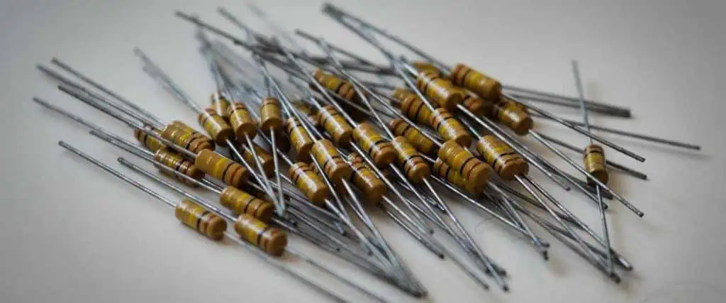
Basic Characteristics of Resistors

Key Physical Properties

PropertyDescriptionSignificance
ResistanceOpposition to current flowDetermines circuit behavior
Power RatingMaximum power dissipationPrevents component failure
ToleranceAccuracy of resistance valueImpacts circuit precision
Temperature CoefficientResistance variation with temperatureCritical for stable performance

Color Code Identification Method

Standard Resistor Color Coding System

Color Band Interpretation

Band PositionMeaningValue Representation
1st BandFirst Significant Digit0-9
2nd BandSecond Significant Digit0-9
3rd BandMultiplierDecimal place shift
4th BandTolerancePercentage accuracy
5th BandTemperature CoefficientPerformance variation

Detailed Color Code Decoding

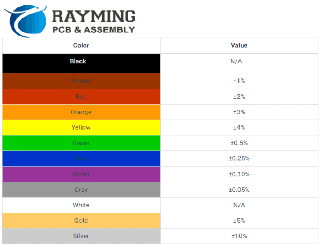
Color to Value Mapping

ColorNumeric ValueMultiplierTolerance
Black0ร— 1ยฑ1%
Brown1ร— 10ยฑ1%
Red2ร— 100ยฑ2%
Orange3ร— 1,000ยฑ3%
Yellow4ร— 10,000ยฑ4%
Green5ร— 100,000ยฑ0.5%
Blue6ร— 1,000,000ยฑ0.25%
Violet7ร— 10,000,000ยฑ0.1%
Gray8ร— 100,000,000ยฑ0.05%
White9ร— 1,000,000,000ยฑ5%

Advanced Identification Techniques

Resistor Temperature Coefficient Color Schemes for Resistance Value

Measurement Tools and Methods

Identification Equipment

ToolPurposeAccuracyRecommended Use
MultimeterResistance Measurementๅค0.1ๆƒŸDirect Resistance Check
LCR MeterPrecise Component Analysisๅค0.1%Comprehensive Testing
Digital CaliperPhysical Dimension Verificationๅค0.01mmSize and Type Confirmation
MicroscopeSurface Detail ExaminationOptical PrecisionFine Detail Analysis

Resistor Type Classification

Comprehensive Resistor Taxonomy

Main Resistor Categories

  1. Fixed Resistors
  2. Variable Resistors
    • Potentiometers
    • Trimpots
    • Rheostats
  3. Special Purpose Resistors

Physical Characteristics Analysis

Dimensional and Structural Identification

Key Physical Indicators

CharacteristicIdentification CriteriaSignificance
Body MaterialCeramic, Plastic, MetalIndicates Construction Type
Terminal StyleAxial, Surface MountMounting Configuration
Body ShapeCylindrical, RectangularDetermines Installation Method
Surface MarkingPrinted Resistance ValuesDirect Identification

Temperature and Environmental Considerations

Factors Affecting Resistor Identification

Environmental Impact Assessment

  1. Temperature Sensitivity
  2. Humidity Resistance
  3. Mechanical Stress Tolerance
  4. Aging Effects

Precision Identification Protocols

100K-Resistor

Step-by-Step Identification Process

Comprehensive Verification Method

  1. Visual Inspection
  2. Color Code Decoding
  3. Dimensional Measurement
  4. Electrical Measurement
  5. Comparative Analysis

Common Identification Challenges

Troubleshooting Identification Difficulties

Resolution Strategies

ChallengeDiagnostic ApproachRecommended Solution
Faded MarkingsMicroscopic ExaminationAlternative Measurement Methods
Surface DamageComparative AnalysisSpecialized Testing Equipment
Unusual ConfigurationsHistorical ReferenceManufacturer Documentation

Advanced Digital Identification Technologies

Emerging Identification Methods

Technological Approaches

  • Machine Learning Recognition
  • Spectral Analysis
  • Computer Vision Techniques
  • Automated Scanning Systems

Professional Best Practices

Recommended Identification Techniques

  1. Use Multiple Verification Methods
  2. Maintain Comprehensive Documentation
  3. Invest in Precision Measurement Tools
  4. Stay Updated on New Technologies

Safety Considerations

Handling and Identification Precautions

Critical Safety Guidelines

  • Use Proper Personal Protective Equipment
  • Avoid Direct Contact with Energized Components
  • Discharge Capacitors Before Measurement
  • Work in Well-Ventilated Areas

Frequently Asked Questions (FAQ)

Q1: How Accurate Are Color Codes for Resistor Identification?

A1: Color codes are generally 95-99% accurate when properly interpreted. However, factors like age, wear, and manufacturing variations can affect precision.

Q2: Can I Identify a Resistor Without a Multimeter?

A2: While a multimeter provides the most accurate measurement, color codes and physical characteristics can offer reliable preliminary identification.

Q3: What’s the Most Common Mistake in Resistor Identification?

A3: Misreading color bands due to improper orientation or misunderstanding the color-to-value mapping is the most frequent identification error.

Q4: How Do Surface Mount Resistors Differ in Identification?

A4: Surface mount resistors typically use numerical codes instead of color bands, requiring different identification techniques and specialized knowledge.

Q5: Are There Universal Identification Standards?

A5: While color coding is widely used, international standards like IEC and ANSI provide comprehensive guidelines for resistor marking and identification.

Conclusion

Resistor identification is a nuanced skill combining visual analysis, technical knowledge, and precision measurement techniques. By understanding the comprehensive approach outlined in this guide, professionals and enthusiasts can confidently and accurately identify resistors across various applications and environments.

Editing PCBs with Gerber Files in Altium: A Comprehensive Workflow Guide

Altium Circuit Maker

The Role of Gerber Files in PCB Design

Gerber files represent a critical standard in electronic design, serving as a universal format for PCB manufacturing documentation. While primarily used for production, these files can also become powerful tools for design reconstruction and modification in advanced PCB design software like Altium Designer.

YouTube video

Gerber File Fundamentals

Technical Characteristics of Gerber Files

File Format Specifications

Gerber File TypeDescriptionTypical Content
RS-274XExtended Gerber FormatLayer information, aperture definitions
RS-274DLegacy Gerber FormatLimited layer details
Extended GerberModern StandardComprehensive layer metadata

Compatibility Considerations

Key Compatibility Factors

  1. Layer Representation
  2. Coordinate Precision
  3. Manufacturing Information
  4. Graphic Primitives

Importing Gerber Files into Altium Designer

Preparation and Initial Steps

File Import Process

  1. Open Altium Designer
  2. Navigate to File Import Options
  3. Select Appropriate Import Wizard

Import Techniques and Strategies

Comprehensive Import Workflow

StepActionConsiderations
1. File SelectionChoose Gerber FilesVerify file completeness
2. Layer MappingAssign Layers CorrectlyMatch original design intent
3. Coordinate CalibrationAdjust Scale and OriginEnsure dimensional accuracy
4. Primitive ConversionTransform Graphic ElementsMaintain original design characteristics

Advanced Editing Techniques

Reconstruction Methodologies

Design Extraction Strategies

  • Layer-by-Layer Analysis
  • Primitive Reconstruction
  • Intelligent Design Inference

Limitations and Challenges

Potential Reconstruction Constraints

ConstraintImpactMitigation Strategy
Limited MetadataIncomplete Design InformationManual Verification
Complex GeometriesDifficult Primitive RecreationAdvanced Tracing Techniques
Missing Layer DetailsPartial Design RepresentationSupplementary Documentation

Workflow Optimization Techniques

Precision Enhancement Methods

Editing Strategies

  1. Dimensional Calibration
  2. Topology Preservation
  3. Signal Integrity Maintenance

Professional Reconstruction Approach

Systematic Verification Process

  • Dimensional Cross-Referencing
  • Signal Path Validation
  • Manufacturing Rule Compliance

Design Rule Checking (DRC) After Reconstruction

Comprehensive Validation Protocols

Critical Verification Parameters

Verification CategoryCheck ParametersAcceptable Tolerance
Trace WidthDimensional Accuracyยฑ10% of Original Design
Clearance SpacingMinimum SeparationIPC-2221 Compliance
Via DimensionsHole Size and Placementยฑ0.05mm Precision
Layer AlignmentInterlayer Registration95-100% Accuracy

Advanced Altium Designer Techniques

Altium Designer 20

Specialized Reconstruction Tools

Software Capabilities

  • Intelligent Layer Inference
  • Automated Primitive Reconstruction
  • Complex Geometry Analysis

Best Practices for Gerber File Editing

Professional Recommendations

  1. Maintain Original Design Intent
  2. Verify Dimensional Accuracy
  3. Use Multiple Reference Sources
  4. Implement Comprehensive DRC

Potential Challenges in Gerber File Editing

Reconstruction Complexity Factors

Key Challenging Aspects

  • Limited Metadata Availability
  • Precision Requirements
  • Complex Multilayer Designs
  • Proprietary Design Elements

Alternative Approaches

Complementary Reconstruction Methods

Supplementary Techniques

  • Original Design File Retrieval
  • Collaborative Manufacturer Consultation
  • Reverse Engineering Strategies

Emerging Technologies in PCB Reconstruction

Future Development Trajectories

Technological Evolution

  • Artificial Intelligence-Assisted Reconstruction
  • Machine Learning Design Inference
  • Advanced Visualization Technologies

Frequently Asked Questions (FAQ)

Q1: Can I Completely Recreate a PCB Design from a Gerber File?

A1: While possible, complete recreation is challenging. Gerber files provide visual and manufacturing information but lack complete schematic and component details. Expect partial reconstruction with potential manual intervention.

Q2: What Are the Primary Limitations of Gerber File Editing?

A2: Limitations include incomplete layer information, potential loss of precise design intent, challenges in reconstructing complex geometries, and absence of original component metadata.

Q3: How Accurate Can Gerber File Reconstruction Be?

A3: Reconstruction accuracy varies, typically ranging from 70-90% depending on design complexity, file quality, and available supplementary documentation.

Q4: Are There Legal Considerations in Reproducing PCB Designs?

A4: Yes, always respect intellectual property rights. Ensure you have proper authorization before attempting to reproduce or modify proprietary PCB designs.

Q5: What Skills Are Required for Effective Gerber File Editing?

A5: Successful editing requires proficiency in PCB design software, understanding of electronic design principles, attention to detailed geometric reconstruction, and comprehensive design rule knowledge.

Conclusion

Editing PCB designs using Gerber files in Altium represents a sophisticated process combining technical expertise, advanced software capabilities, and meticulous attention to design reconstruction strategies. While challenging, it offers powerful opportunities for design analysis, modification, and preservation.

Mastering Circuit CAM: A Comprehensive Guide to Computer-Aided Manufacturing in Electronics Design

Computer-Aided Manufacturing (CAM) has revolutionized the electronics design and production landscape. Circuit CAM represents a critical interface between electronic design automation (EDA) and manufacturing processes, enabling precise translation of circuit designs into physical manufacturing instructions.

Understanding Circuit CAM Fundamentals

What is Circuit CAM?

Circuit CAM is specialized software that transforms electronic design files into manufacturing-ready instructions for printed circuit board (PCB) production. It serves as a crucial bridge between design conceptualization and physical manufacturing, ensuring accuracy and efficiency in the production process.

YouTube video

Key Components of Circuit CAM Systems

Core Functional Elements

ComponentPrimary FunctionCritical Characteristics
Design Import ModuleTranslates design filesSupports multiple file formats (Gerber, ODB++, DXF)
Design Rule Checking (DRC)Validates design manufacturabilityIdentifies potential fabrication issues
Manufacturing Output GeneratorCreates production instructionsGenerates toolpaths, drill files, and layer specifications
Optimization EngineImproves manufacturing efficiencyMinimizes material waste, reduces production time

Detailed Workflow of Circuit CAM Software

Design Preparation Stage

File Conversion and Standardization

  1. Import design files from EDA tools
  2. Verify file integrity
  3. Convert to manufacturing-compatible formats

Design Rule Checking (DRC) Process

Comprehensive Validation Criteria

Validation CategoryCheck ParametersAcceptable Tolerance
Minimum Trace WidthCircuit trace dimensionsยฑ10% of design specification
Clearance SpacingDistance between circuit elementsMeets IPC-2221 standards
Drill Hole SizesMounting and via hole dimensionsยฑ0.05mm precision
Copper Pour IntegrityContinuous copper layer coverage95-100% coverage requirement

Advanced Circuit CAM Techniques

Figure 5 CamTastic complete PCB view

Automated Manufacturing Optimization

Intelligent Path Generation

  • Minimizes tool changes
  • Reduces machining time
  • Optimizes material utilization

Layer Management Strategies

Multilayer PCB Processing

  1. Precise layer alignment
  2. Accurate registration marks
  3. Consistent inter-layer connections

Equipment Compatibility and Integration

Software and Hardware Synchronization

Supported Manufacturing Equipment

Equipment TypeTypical CompatibilityCommunication Protocol
CNC Milling MachinesHighG-code, HPGL
Laser Cutting SystemsModerate to HighDXF, Gerber Extended
3D Printing PlatformsEmergingSTL, OBJ
Automated Optical InspectionHighXML, CSV

Troubleshooting Common Circuit CAM Challenges

Frequent Manufacturing Issues and Solutions

Problem Resolution Matrix

IssueRoot CauseRecommended Solution
Design Import ErrorsIncompatible File FormatsUse Universal Conversion Utilities
Unexpected Tool PathsIncorrect Machine CalibrationRecalibrate Machine Parameters
Layer MisalignmentImprecise RegistrationImplement Advanced Alignment Algorithms
Unexpected Copper RemovalIncorrect Etching ParametersRefine Design Rule Checking Protocols

Best Practices in Circuit CAM Utilization

Optimization Strategies

  1. Continuous Software Updates
  2. Regular Calibration
  3. Comprehensive Training
  4. Cross-Platform Compatibility

Advanced Configuration Techniques

Customization and Personalization

Configuration Parameters

Parameter CategoryCustomization OptionsPerformance Impact
Tool Path GenerationAggressive, Conservative, BalancedDirectly affects machining speed
Tolerance SettingsTight, Standard, LooseInfluences manufacturing precision
Material CompensationAdaptive AlgorithmsImproves yield and quality

Safety and Compliance Considerations

Regulatory and Operational Guidelines

Key Compliance Frameworks

Corne PCB Layout
Corne PCB Layout

Risk Mitigation Strategies

  1. Regular software validation
  2. Comprehensive backup protocols
  3. Secure data management

Emerging Technologies in Circuit CAM

Future Development Trajectories

Technological Evolution

Frequently Asked Questions (FAQ)

Q1: What is the primary difference between EDA and CAM software?

A1: Electronic Design Automation (EDA) focuses on design creation, while Computer-Aided Manufacturing (CAM) translates those designs into precise manufacturing instructions, bridging the gap between conceptual design and physical production.

Q2: How often should Circuit CAM software be updated?

A2: Recommended update frequency is quarterly or with each major version release. Always ensure compatibility with your specific manufacturing equipment and design requirements.

Q3: Can Circuit CAM handle complex multilayer PCB designs?

A3: Modern Circuit CAM solutions are designed to manage intricate multilayer designs with advanced layer management, registration, and alignment capabilities.

Q4: What file formats are typically supported by Circuit CAM?

A4: Standard supported formats include Gerber (RS-274X), ODB++, DXF, AutoCAD, and various proprietary EDA tool export formats.

Q5: How do I ensure optimal manufacturing results with Circuit CAM?

A5: Ensure comprehensive design rule checking, maintain updated software, perform regular calibrations, and invest in continuous training for design and manufacturing teams.

Conclusion

Circuit CAM represents a sophisticated intersection of design intelligence and manufacturing precision. By understanding its comprehensive capabilities, engineers and manufacturers can transform complex electronic designs into high-quality, reliable products with unprecedented efficiency.

Mastering PCB Etching Chops: A Comprehensive Guide to Precision Map Making

Printed Circuit Board (PCB) etching is a critical process in electronics manufacturing that requires meticulous attention to detail and precision. This comprehensive guide will explore the intricate world of testing etching chops through advanced map making techniques, providing engineers, technicians, and electronics enthusiasts with a deep understanding of the methodology, challenges, and best practices.

Understanding PCB Etching Fundamentals

The Science Behind PCB Etching

PCB etching is a chemical process that selectively removes copper from a substrate to create precise circuit patterns. The etching chops, or areas of copper removal, are crucial in determining the accuracy and quality of the final printed circuit board.

Key Components of the Etching Process

YouTube video

Etching Materials and Chemicals

The etching process typically involves several critical components:

ComponentFunctionTypical Specifications
Copper Clad SubstrateBase material1 oz, 2 oz copper thickness
Etchant SolutionChemical removal of copperFerric Chloride or Ammonium Persulfate
Resist MaterialProtects areas from etchingPhotoresist or Dry Film
Etching ChopsPrecisely defined removal areasVaries by design complexity

Mapping Techniques for Precise Etching Chops

Digital Mapping Strategies

Advanced CAD and CAM Integration

Modern PCB map making relies on sophisticated computer-aided design (CAD) and computer-aided manufacturing (CAM) tools to create precise etching maps.

Mapping Accuracy Factors

  1. Resolution Capabilities
  2. Registration Precision
  3. Design Rule Checking (DRC)
  4. Gerber File Accuracy

Testing Methodologies for Etching Chops

Comprehensive Testing Protocols

Visual Inspection Techniques

  1. Microscopic examination
  2. Dimensional verification
  3. Surface continuity checks

Quantitative Testing Metrics

Testing MetricAcceptable RangeMeasurement Method
Line Width Toleranceยฑ10% of designOptical Microscopy
Copper Thickness Retention90-95%Eddy Current Testing
Surface Roughness<2.5 ฮผmProfilometer

Advanced Diagnostic Approaches

Non-Destructive Testing Methods

  • X-ray inspection
  • Automated optical inspection (AOI)
  • Electrical continuity testing

Troubleshooting Common Etching Challenges

Identifying and Resolving Etching Defects

Common Etching Defects

  1. Over-etching
  2. Under-etching
  3. Edge roughness
  4. Copper lift-off

Mitigation Strategies

  1. Optimize etchant concentration
  2. Control etching temperature
  3. Implement precise time management
  4. Use high-quality resist materials

Equipment and Tools for Precision Etching

Essential Equipment Checklist

Equipment CategoryRecommended SpecificationsPurpose
Etching TankTemperature-controlledConsistent chemical processing
Microscope100x-500x magnificationDetailed inspection
Precision Scale0.01g accuracyChemical measurement
UV Exposure UnitControlled wavelengthResist curing

Advanced Techniques in PCB Etching Map Making

Computational Mapping Approaches

Machine Learning Integration

Emerging technologies are revolutionizing PCB map making through:

  • Predictive defect analysis
  • Automated design optimization
  • Real-time process monitoring

Safety and Environmental Considerations

Strip film etching line

Handling Etching Chemicals

Safety Protocols

  1. Personal protective equipment (PPE)
  2. Proper chemical storage
  3. Waste disposal regulations

Environmental Compliance

  • Chemical neutralization techniques
  • Recycling of etching solutions
  • Minimizing chemical waste

Frequently Asked Questions (FAQ)

Q1: What is the most critical factor in PCB etching chop accuracy?

A1: The most critical factor is the precision of your digital design and the quality of the resist material. Accurate CAD files and high-resolution photoresist application are key to achieving precise etching chops.

Q2: How often should etching equipment be calibrated?

A2: Professional facilities should calibrate etching equipment quarterly, with monthly preliminary checks. For smaller operations, bi-annual calibration is typically sufficient.

Q3: Can I reuse etching solutions?

A3: Etching solutions can be reused, but their effectiveness diminishes with each use. Implement a systematic monitoring process to track solution concentration and replace when performance degrades.

Q4: What are the signs of a poor etching process?

A4: Indicators include inconsistent line widths, rough board edges, copper residue, incomplete pattern transfer, and visible under or over-etching.

Q5: How do environmental conditions affect etching?

A5: Temperature, humidity, and chemical concentration significantly impact etching quality. Maintain a stable environment with controlled temperature (20-25ยฐC) and minimal humidity fluctuations.

Conclusion

Mastering PCB etching chops through advanced map making requires a multifaceted approach combining technological expertise, precise measurement, and continuous learning. By implementing the strategies outlined in this guide, professionals can achieve exceptional results in printed circuit board manufacturing.

How to Synchronize PADS Logic and PADS Layout: A Comprehensive Guide

Importance of Synchronization

The synchronization between PADS Logic and PADS Layout ensures design consistency throughout the PCB development process. Proper synchronization prevents errors, reduces design time, and maintains data integrity between schematic and layout phases.

YouTube video

Basic Concepts and Terminology

TermDescriptionRelevance
Forward AnnotationChanges from Logic to LayoutComponent updates, nets
Back AnnotationChanges from Layout to LogicPin swapping, names
ECOEngineering Change OrderTrack design changes
Design SyncBidirectional updateComplete synchronization

Preparation for Synchronization

File Structure Requirements

File TypeExtensionPurpose
Schematic.schCircuit design
Layout.pcbBoard layout
Library.libComponent definitions
NetList.netConnectivity information
ECO.ecoChange documentation

Project Setup Guidelines

SettingDescriptionRecommendation
Project PathFile locationUse common root directory
Library PathComponent librariesMaintain consistent paths
BackupAuto-save settingsEnable regular backups
Version ControlFile managementUse revision tracking

Forward Annotation Process

Steps for Forward Annotation

Pre-Annotation Checklist

Check ItemDescriptionAction Required
DRCDesign Rule CheckRun and resolve errors
LibraryComponent checkVerify all parts exist
NetsSignal definitionsConfirm naming conventions
PowerPower/ground setupVerify connections

Component Management

AspectLogic RequirementsLayout Requirements
FootprintsAssigned in LogicMatch in Layout
ReferencesUnique designatorsConsistent naming
AttributesProperty definitionsMatching properties
PlacementRough placementFinal position

Back Annotation Process

Layout to Logic Updates

Update TypeDescriptionSynchronization Method
Pin SwapsGate/pin changesAutomatic update
Reference ChangesDesignator updatesManual verification
Net NamesSignal namingBidirectional sync
PropertiesComponent attributesSelective update

Verification Process

StepTool/MethodPurpose
CompareBuilt-in compareIdentify differences
ValidateDRC checkVerify rules compliance
ReviewVisual inspectionConfirm changes
DocumentChange logTrack modifications

Advanced Synchronization Techniques

ECO Management

ECO TypeApplicationHandling Method
ComponentPart changesForward annotation
NetworkConnection updatesBidirectional sync
PropertyAttribute changesSelective update
PlacementPosition changesBack annotation

Batch Processing

ProcessDescriptionBest Practice
ScriptAutomated updatesUse for repetitive tasks
Batch ECOMultiple changesGroup related updates
Mass UpdateGlobal changesCareful validation

Common Synchronization Issues

Issue Resolution Table

IssueCauseResolution
Missing ComponentsLibrary mismatchUpdate libraries
Net MismatchesNaming conflictsStandardize naming
Property ConflictsInconsistent attributesAlign properties
Update FailuresFile access issuesCheck permissions

Prevention Strategies

StrategyImplementationBenefit
Regular SyncSchedule updatesPrevent large deltas
Library ControlCentralized managementConsistency
Naming StandardsDocumented conventionsReduce conflicts
Version ControlChange trackingRecovery options

Best Practices for Maintaining Synchronization

Project Organization

AspectRecommendationPurpose
File StructureHierarchical organizationEasy navigation
NamingConsistent conventionsClear identification
BackupsRegular archivesData protection
DocumentationChange recordsTrack history

Quality Control Measures

MeasureFrequencyPurpose
DRC CheckBefore/After syncVerify integrity
Library AuditMonthlyMaintain consistency
Sync ReviewEach major changeValidate updates
Backup VerifyWeeklyEnsure recovery

Tools and Automation

Built-in PADS Tools

ToolPurposeBest Use Case
CompareDesign comparisonChange verification
ECO GeneratorChange managementDesign updates
DRCRule checkingQuality control
Report GeneratorDocumentationChange tracking

Custom Solutions

SolutionApplicationBenefit
ScriptsAutomated tasksEfficiency
CheckersCustom validationSpecific rules
ReportsCustom documentationDetailed tracking

Frequently Asked Questions

Q1: How often should I synchronize PADS Logic and Layout?

A: Synchronization frequency depends on:

  • Project complexity
  • Team size
  • Development phase
  • Change frequency

Best practices recommend:

  • Daily sync for active development
  • After major changes
  • Before releasing documentation
  • When switching between Logic and Layout work

Q2: What are the most common synchronization errors?

A: Common synchronization errors include:

  • Component library mismatches
  • Net name conflicts
  • Missing footprint assignments
  • Property inconsistencies
  • File access problems

To prevent these, maintain:

  • Updated libraries
  • Consistent naming conventions
  • Regular synchronization
  • Proper file permissions

Q3: How can I verify successful synchronization?

A: Verification steps include:

  1. Run DRC in both Logic and Layout
  2. Compare netlists
  3. Check ECO reports
  4. Verify component counts
  5. Review critical nets
  6. Check property transfers

Q4: What should I do if synchronization fails?

A: Follow these steps:

  1. Document the error message
  2. Check file permissions
  3. Verify library accessibility
  4. Review recent changes
  5. Use backup files if necessary
  6. Contact technical support if needed

Q5: How do I handle partial updates during synchronization?

A: For partial updates:

  1. Use selective synchronization
  2. Create specific ECOs
  3. Verify affected areas
  4. Document changes
  5. Test functionality
  6. Update related documentation

Conclusion

Successful synchronization between PADS Logic and Layout requires careful attention to detail, consistent procedures, and regular verification. By following these guidelines and best practices, you can maintain design integrity throughout the PCB development process. Remember to regularly backup your work, document changes, and verify synchronization results to ensure successful project completion.

How to Read a PCB Fabrication Drawing: A Comprehensive Guide

Purpose and Importance

PCB fabrication drawings, also known as PCB mechanical drawings or PCB assembly drawings, are essential technical documents that provide detailed specifications for manufacturing printed circuit boards. These drawings serve as a communication bridge between PCB designers and manufacturers, ensuring accurate production of the intended design.

YouTube video

Basic Components of a Fabrication Drawing

Component Description Purpose
Title Block Project information and revisions Identification and version control
Board Outline Physical dimensions and shape Define board boundaries
Layer Stack-up Material and copper layer details Specify board construction
Drill Table Hole sizes and quantities Define drilling requirements
Notes Special requirements and specifications Clarify manufacturing details
Tolerances Acceptable variation ranges Quality control parameters

Title Block Information

Essential Title Block Elements

Element Description Example
Drawing Number Unique identifier DWG-2024-001
Revision Level Version control Rev. A
Date Creation/revision date 25-Nov-24
Engineer Designer name John Smith
Scale Drawing scale ratio 1:01
Sheet Number Page information 1 of 3

Board Outline Specifications

Dimensional Information

Aspect Common Units Typical Tolerance
Length mm/inches ยฑ0.1mm/ยฑ0.004″
Width mm/inches ยฑ0.1mm/ยฑ0.004″
Thickness mm/inches ยฑ10%
Corner Radius mm/inches ยฑ0.1mm/ยฑ0.004″

Board Profile Features

Feature Description Specification Method
Cutouts Internal board openings Dimensions from datum
Notches Edge indentations Size and position
Chamfers Edge angles Angle and length
Slots Linear openings Width and length

Layer Stack-up Information

Standard Layer Stack-up Table

Layer Material Thickness Description
Top Solder Mask LPI 0.01mm Green
Top Copper Copper 1oz (35ยตm) Signal
Prepreg FR4 0.2mm Dielectric
Inner Layer 1 Copper 0.5oz (17.5ยตm) Ground
Core FR4 0.4mm Substrate
Inner Layer 2 Copper 0.5oz (17.5ยตm) Power
Prepreg FR4 0.2mm Dielectric
Bottom Copper Copper 1oz (35ยตm) Signal
Bottom Solder Mask LPI 0.01mm Green

Material Specifications

Property Unit Common Values
Dielectric Constant Er 3.5-4.5
Glass Transition Temp Tg 130-170ยฐC
Thermal Conductivity W/mยทK 0.25-0.5
Copper Weight oz/ftยฒ 0.5-2.0

Drill Information

Drill Table Components

Column Description Example
Symbol Drill identifier โŒ€1, โŒ€2
Size Hole diameter 0.3mm
Quantity Number of holes 150
Plating Plating requirement PTH/NPTH
Tolerance Size variation ยฑ0.05mm

Common Drill Types

Type Description Typical Use
PTH Plated Through Hole Component leads
NPTH Non-Plated Through Hole Mounting holes
Blind Via Partial depth connection HDI designs
Buried Via Internal layer connection Complex routing

Special Requirements

Surface Finish Specifications

Finish Type Thickness Application
HASL 0.5-1.0ยตm General purpose
ENIG 3-6ยตm Ni, 0.05-0.1ยตm Au Fine pitch
OSP 0.2-0.5ยตm Lead-free
Immersion Tin 0.8-1.2ยตm Good solderability

Solder Mask Specifications

Parameter Specification Notes
Color Green, Red, Blue, etc. UV blocking
Type LPI, dry film Process dependent
Thickness 0.02-0.04mm Coverage
Registration ยฑ0.1mm Alignment

Manufacturing Notes

Standard Note Categories

Category Purpose Example Notes
Material Specify board material “Use TG170 FR4”
Finish Surface treatment “ENIG per IPC-4552”
Testing Test requirements “100% E-test required”
Marking Board identification “UL mark required”

Critical Parameters

Parameter Typical Range Description
Impedance Control ยฑ10% Signal integrity
Copper Thickness ยฑ10% Current capacity
Registration ยฑ0.075mm Layer alignment
Hole Quality Class 2/3 IPC standards

Quality Specifications

IPC Standards Reference

Standard Topic Application
IPC-6012 Rigid PCB qualification General requirements
IPC-A-600 Acceptability criteria Visual inspection
IPC-TM-650 Test methods Quality verification
IPC-4101 Base materials Material specs

Inspection Requirements

Aspect Method Criteria
Registration Optical ยฑ0.075mm max
Hole Size Gauge pins +0.075/-0.0mm
Surface Finish XRF measurement Per specification
Cleanliness Ion chromatography <1.0 ยตg/inยฒ NaCl

Frequently Asked Questions

Q1: What are the most important elements to check in a PCB fabrication drawing?

A: The critical elements to verify include:

  • Board dimensions and tolerances
  • Layer stack-up details
  • Drill specifications
  • Material requirements
  • Surface finish specifications
  • Special notes and requirements Always cross-reference these with your manufacturer’s capabilities.

Q2: How do I interpret drill table symbols and specifications?

A: Drill tables typically include:

  • Drill size (diameter)
  • Quantity of each size
  • Plating requirements (PTH/NPTH)
  • Special requirements (depth for blind vias)
  • Tolerance specifications Look for the corresponding symbols on the drawing to locate each hole type.

Q3: What is the significance of the layer stack-up table?

A: The layer stack-up table defines:

  • Number of copper layers
  • Layer thicknesses
  • Material types
  • Dielectric specifications
  • Overall board thickness This information is crucial for impedance control and manufacturing process planning.

Q4: How do I verify dimensional tolerances?

A: To verify tolerances:

  1. Check the general tolerance note
  2. Look for specific critical tolerances
  3. Compare with manufacturer capabilities
  4. Consider cumulative tolerances
  5. Verify against assembly requirements

Q5: What common mistakes should I watch for when reading fabrication drawings?

A: Common oversights include:

  • Missing or incorrect revision numbers
  • Conflicting specifications
  • Unclear special requirements
  • Incomplete drill information
  • Missing critical dimensions Always cross-reference with other documentation and verify completeness.

Conclusion

Reading PCB fabrication drawings requires attention to detail and understanding of various technical specifications. The ability to interpret these drawings accurately is crucial for successful PCB manufacturing. Always verify critical parameters, cross-reference specifications with manufacturer capabilities, and ensure all special requirements are clearly communicated. When in doubt, consult with your PCB manufacturer for clarification on any aspects of the fabrication drawing.

How to Program FPGA by Yourself: A Complete Guide

Field-Programmable Gate Arrays (FPGAs) are semiconductor devices consisting of configurable logic blocks connected through programmable interconnects. Unlike microprocessors that execute sequential instructions, FPGAs can implement any digital logic function through parallel processing, making them incredibly versatile for various applications.

YouTube video

Key FPGA Components

ComponentDescriptionPurpose
Logic Elements (LEs)Basic building blocksImplement combinational and sequential logic
Look-Up Tables (LUTs)Truth table implementationDefine logic functions
Flip-FlopsStorage elementsStore binary states
I/O BlocksInterface componentsConnect FPGA to external devices
Clock NetworksSignal distributionSynchronize operations
Memory BlocksStorage arraysStore data and instructions

Getting Started with FPGA Programming

Essential Tools and Software

CategoryRequired ToolsPurpose
Hardware Description LanguageVHDL/Verilog EditorCode development
Synthesis ToolVendor-specific (e.g., Vivado, Quartus)Convert HDL to netlist
Simulation SoftwareModelSim, GHDLVerify design behavior
Programming CableUSB Blaster, JTAGDownload design to FPGA
Development BoardStarter kitHardware platform

Choosing Your First FPGA

ManufacturerEntry-Level BoardFeaturesBest For
XilinxArtix-7Moderate resources, good docsGeneral learning
Intel (Altera)Cyclone IVCost-effective, simpleBeginners
LatticeiCE40Ultra-low power, compactSimple projects

HDL Programming Fundamentals

VHDL vs. Verilog Comparison

AspectVHDLVerilog
OriginMilitary/AerospaceCommercial/Industry
SyntaxAda-like, verboseC-like, concise
Type SystemStrongly typedLoosely typed
Learning CurveSteeperModerate
Debug CapabilityBetterGood

Basic HDL Concepts

Common HDL Structures

StructurePurposeExample Usage
Entity/ModuleDefine interfacePort declarations
Architecture/ImplementationDescribe behaviorLogic implementation
Process/AlwaysSequential logicState machines
Concurrent StatementsCombinational logicDirect assignments

Design Methodology

Design Flow Steps

  1. Specification
  2. HDL Coding
  3. Simulation
  4. Synthesis
  5. Implementation
  6. Timing Analysis
  7. Programming
  8. Verification

Design Best Practices

Coding Guidelines

AspectRecommendationReason
Clock DomainsMinimize numberReduce complexity
SynchronizationUse proper techniquesPrevent metastability
Resource UsageMonitor utilizationOptimize performance
DocumentationComment thoroughlyMaintain code

Advanced FPGA Concepts

Memory Types and Usage

Memory TypeCharacteristicsBest Use Case
Distributed RAMFast, small capacityLocal storage
Block RAMLarger, dedicatedData buffers
Shift RegistersSequential accessFIFO, delays
External MemoryHighest capacityMass storage

Clock Management

Clock Domain Considerations

AspectImplementationPurpose
PLL/DLLClock multiplication/divisionFrequency synthesis
Clock GatingEnable/disable clocksPower management
Clock CrossingSynchronization circuitsMulti-domain designs

Implementation Techniques

ic programming services

State Machine Design

TypeCharacteristicsBest For
MealyOutput depends on inputsProtocol handling
MooreOutput depends on statePredictable timing
HybridCombines bothComplex control

Common Design Patterns

PatternUse CaseBenefits
PipelineData processingHigher throughput
FIFOData bufferingClock domain crossing
ArbiterResource sharingMulti-master systems

Debugging and Verification

Simulation Strategies

LevelPurposeTools
BehavioralFunctional verificationHDL simulator
Post-synthesisLogic verificationVendor tools
Post-implementationTiming verificationTiming analyzer

Debug Tools

Tool TypeFeaturesApplication
Logic AnalyzerSignal captureRuntime debug
ChipScope/SignalTapInternal probingDeep debug
JTAGBoundary scanBoard test

Project Examples

Beginner Projects

ProjectComplexitySkills Learned
LED ControllerLowBasic I/O, counters
UART InterfaceMediumSerial protocols
Simple ALUMediumCombinational logic
VGA ControllerHighTiming, memory

Frequently Asked Questions

Q1: How long does it take to learn FPGA programming?

A: Learning FPGA programming typically takes 3-6 months to grasp the basics and 1-2 years to become proficient. The learning curve depends on:

  • Prior digital design experience
  • Programming background
  • Time commitment
  • Project complexity level

Q2: Which HDL should I learn first – VHDL or Verilog?

A: For beginners, Verilog is often recommended because:

  • More C-like syntax feels familiar to software developers
  • Less verbose than VHDL
  • Widely used in industry
  • More flexible for small projects However, both languages are equally capable, and the choice often depends on your region and industry.

Q3: What are the common mistakes beginners make in FPGA design?

A: Common beginner mistakes include:

  • Thinking in software terms instead of hardware
  • Improper clock domain crossing
  • Inadequate timing constraints
  • Not considering hardware resources
  • Insufficient simulation testing

Q4: What computer specifications are needed for FPGA development?

A: Recommended specifications:

  • Processor: Modern multi-core CPU (i5/i7 or equivalent)
  • RAM: Minimum 16GB, 32GB recommended
  • Storage: 256GB+ SSD
  • OS: Windows 10/11 or Linux
  • Multiple monitors recommended

Q5: How do I choose the right FPGA for my project?

A: Consider these factors:

  • Logic element count needed
  • Memory requirements
  • I/O pin count
  • Speed requirements
  • Power constraints
  • Cost limitations
  • Development tool availability

Conclusion

FPGA programming is a valuable skill that combines hardware and software concepts. Starting with basic projects and gradually moving to more complex designs while following best practices will help you build expertise. Remember that FPGA development is an iterative process that requires patience and thorough testing at each stage. Keep practicing, stay updated with new tools and techniques, and join FPGA communities for support and knowledge sharing.

What is the shelf life of Flex PCB?

Key components of Flex PCBs

  1. Substrate: Usually made of polyimide or polyester
  2. Conductors: Typically copper traces
  3. Coverlay: Protective layer similar to solder mask on rigid PCBs
  4. Adhesives: Used to bond layers together
  5. Surface finishes: Protect exposed copper and improve solderability

Factors Affecting Flex PCB Shelf Life

The shelf life of Flexible PCBs can be influenced by various factors. Understanding these factors is crucial for proper storage and handling.

1. Material Composition

The materials used in Flex PCBs play a significant role in determining their shelf life. Here’s a breakdown of common materials and their typical shelf lives:

MaterialTypical Shelf LifeNotes
Polyimide1-2 yearsMore resistant to environmental factors
Polyester6-12 monthsLess resistant to humidity and temperature changes
Copper1-2 yearsDepends on surface finish
Adhesives6-18 monthsVaries by type and environmental conditions
Surface finishes6-24 monthsDepends on the specific finish used

2. Environmental Factors

Environmental conditions can significantly impact the shelf life of Flex PCBs:

Temperature

High temperatures can accelerate degradation of materials, particularly adhesives and certain surface finishes.

Humidity

Excessive moisture can lead to oxidation of copper traces and delamination of layers.

Light Exposure

UV light can cause degradation of some polymer materials used in Flex PCBs.

Air Quality

Pollutants and corrosive gases can affect the surface finishes and copper traces.

3. Storage Conditions

Proper storage is crucial for maximizing the shelf life of Flex PCBs:

Storage ConditionRecommended RangeImpact on Shelf Life
Temperature20-25ยฐC (68-77ยฐF)ยฑ5ยฐC can double or halve shelf life
Relative Humidity30-50%Higher humidity reduces shelf life
Light ExposureMinimalDirect sunlight can reduce shelf life by 50%
Air QualityClean, dry airPollutants can reduce shelf life by 25-75%

4. Handling and Packaging

Proper handling and packaging can significantly extend the shelf life of Flex PCBs:

  • Use of moisture-barrier bags
  • Inclusion of desiccants and humidity indicator cards
  • Proper labeling with date of manufacture and storage recommendations
  • Minimizing physical stress during storage and transportation

Typical Shelf Life of Flex PCBs

The shelf life of Flex PCBs can vary widely depending on the factors mentioned above. However, here’s a general guideline:

Type of Flex PCBTypical Shelf LifeNotes
Standard polyimide-based12-24 monthsUnder optimal storage conditions
Polyester-based6-12 monthsMore sensitive to environmental factors
High-reliability (space/medical grade)24-36 monthsStricter manufacturing and storage standards
With sensitive components6-12 monthsDepends on the most sensitive component

It’s important to note that these are general guidelines, and actual shelf life can vary based on specific materials, manufacturing processes, and storage conditions.

Extending the Shelf Life of Flex PCBs

There are several strategies that can be employed to extend the shelf life of Flex PCBs:

1. Proper Storage Techniques

  • Use climate-controlled storage areas
  • Implement proper inventory management (FIFO – First In, First Out)
  • Use specialized packaging materials (moisture-barrier bags, desiccants)

2. Regular Inspection and Testing

  • Implement a schedule for visual inspections
  • Conduct electrical testing on a sample basis
  • Use specialized equipment like moisture analyzers

3. Repackaging and Rebaking

  • Repackage PCBs in fresh moisture-barrier bags periodically
  • Use baking processes to remove absorbed moisture when necessary

4. Surface Finish Selection

Choose surface finishes that offer longer shelf life:

Surface FinishTypical Shelf LifeNotes
ENIG (Electroless Nickel Immersion Gold)12-24 monthsGood oxidation resistance
HASL (Hot Air Solder Leveling)6-12 monthsLess consistent, but can be refreshed
OSP (Organic Solderability Preservative)3-6 monthsShorter shelf life, but environmentally friendly
Immersion Tin6-12 monthsGood for fine-pitch components
Immersion Silver3-6 monthsProne to tarnishing

Impact of Exceeding Shelf Life

Using Flex PCBs beyond their recommended shelf life can lead to various issues:

1. Solderability Problems

  • Poor wetting during soldering
  • Increased risk of solder joint failures

2. Delamination

  • Separation of layers due to adhesive degradation
  • Can lead to electrical and mechanical failures

3. Oxidation

  • Copper traces may oxidize, leading to connectivity issues
  • Can affect the performance of surface-mounted components

4. Mechanical Issues

  • Reduced flexibility
  • Increased risk of cracks or breaks during assembly or use

Best Practices for Managing Flex PCB Shelf Life

To ensure the quality and reliability of Flex PCBs, consider the following best practices:

  1. Implement a robust inventory management system
  2. Train staff on proper handling and storage procedures
  3. Maintain detailed records of manufacturing dates and storage conditions
  4. Develop a testing and inspection protocol for aged PCBs
  5. Work closely with suppliers to understand and optimize shelf life
  6. Consider just-in-time manufacturing to minimize storage time

Conclusion

Understanding and managing the shelf life of Flex PCBs is crucial for ensuring the quality and reliability of electronic products. By considering factors such as material composition, environmental conditions, and storage practices, manufacturers and users can maximize the usable life of these versatile components. Regular inspection, proper handling, and adherence to best practices can help mitigate the risks associated with using aged Flex PCBs and ensure optimal performance in the final application.

Frequently Asked Questions (FAQ)

1. How can I tell if a Flex PCB has exceeded its shelf life?

While it’s not always visually apparent, signs that a Flex PCB may have exceeded its shelf life include:

  • Discoloration or tarnishing of surface finishes
  • Stiffness or brittleness of the flexible substrate
  • Delamination or separation of layers
  • Poor solderability during assembly

If you suspect a Flex PCB has exceeded its shelf life, it’s best to conduct electrical testing and consult with the manufacturer before use.

2. Can I use a Flex PCB that has exceeded its recommended shelf life?

It’s generally not recommended to use Flex PCBs that have exceeded their shelf life, as it can lead to reliability issues. However, if necessary, you may be able to recondition the PCB through processes like baking to remove moisture or re-finishing the surface. Always consult with the manufacturer and conduct thorough testing before using an aged Flex PCB in a critical application.

3. How does the shelf life of Flex PCBs compare to rigid PCBs?

Flex PCBs typically have a shorter shelf life compared to rigid PCBs due to their more sensitive materials and construction. While rigid PCBs made with FR-4 can often last 2-5 years under proper storage conditions, Flex PCBs usually have a shelf life of 1-2 years. The difference is primarily due to the flexible substrate materials and adhesives used in Flex PCBs, which are more susceptible to environmental factors.

4. Are there any industry standards for Flex PCB shelf life?

While there isn’t a single, universally accepted standard for Flex PCB shelf life, several industry guidelines provide recommendations. These include:

  • IPC-1601: Printed Board Handling and Storage Guidelines
  • IPC-6013: Qualification and Performance Specification for Flexible/Rigid-Flexible Printed Boards
  • JEDEC J-STD-033: Handling, Packing, Shipping and Use of Moisture/Reflow Sensitive Surface Mount Devices

These standards provide guidance on storage conditions, handling procedures, and moisture sensitivity levels that can impact shelf life.

5. How does the application of the Flex PCB affect its shelf life considerations?

The intended application of a Flex PCB can significantly influence shelf life considerations:

  • High-reliability applications (e.g., aerospace, medical devices) may require stricter storage conditions and shorter shelf life limits to ensure peak performance.
  • Consumer electronics may have more lenient shelf life requirements but should still adhere to best practices.
  • Applications involving extreme environments (high temperature, high humidity) may necessitate more frequent replacement of stored PCBs.
  • Products with long service lives may require special considerations for long-term storage of spare or replacement Flex PCBs.

Always consider the specific requirements of your application when determining appropriate shelf life limits and storage conditions for Flex PCBs.

How to Panelize Gerber Files: A Comprehensive Guide

Panelization is the process of arranging multiple PCB designs into a single panel for efficient manufacturing. This technique reduces production costs, improves manufacturing efficiency, and ensures consistent quality across all boards. Whether you’re a hobbyist or professional PCB designer, understanding proper panelization techniques is crucial for successful PCB production.

The Importance of Proper Panelization

Proper panelization offers several key benefits:

  • Cost reduction through optimized material usage
  • Improved manufacturing efficiency
  • Better quality control
  • Reduced handling damage
  • Simplified assembly processes

YouTube video

Essential Panelization Parameters

PCB panelization

Panel Size Considerations

The standard panel sizes vary depending on your manufacturer’s capabilities and requirements. Here’s a typical breakdown:

Panel Size (mm)Common ApplicationsTypical Board CountManufacturing Method
457 x 305Large production4-12 boardsAutomated assembly
305 x 254Medium production2-8 boardsMixed assembly
254 x 203Small production1-4 boardsManual assembly
152 x 152Prototyping1-2 boardsManual assembly

Board Spacing Requirements

Proper spacing between boards is crucial for successful manufacturing. Here are the recommended specifications:

ElementMinimum Spacing (mm)Optimal Spacing (mm)Maximum Spacing (mm)
Board-to-Board235
Board-to-Edge57.510
Route Channel22.53
Fiducial Margin57.510

Step-by-Step Panelization Process

1. Pre-Panelization Preparation

Before starting the panelization process, ensure you have:

  • Completed and validated individual PCB designs
  • Confirmed manufacturer’s requirements
  • Determined production volume
  • Selected appropriate panel size
  • Gathered necessary design tools

2. Choosing the Right Panelization Method

Mouse-Bite Method

The mouse-bite method uses small routed holes to create break-away tabs. This approach offers:

  • Clean separation
  • Minimal board edge damage
  • Easy manual separation
  • Good for both prototype and production runs

V-Score Method

V-scoring creates a groove on both sides of the panel, allowing for easy separation:

  • Straight-line breaks only
  • Excellent for rectangular boards
  • Higher production efficiency
  • Better for larger production runs

3. Panel Layout Optimization

Efficiency Calculations

Use this formula to calculate panel efficiency:

ParameterFormulaTarget Percentage
Material Utilization(Total Board Area / Panel Area) ร— 100> 70%
Production Efficiency(Usable Boards / Total Possible Boards) ร— 100> 90%
Waste Factor(Unused Area / Total Panel Area) ร— 100< 30%

4. Adding Manufacturing Elements

Required Panel Features

FeaturePurposePlacement Guidelines
FiducialsAlignment reference for assemblyMinimum 3 per panel, corners preferred
Tooling HolesPanel handling and registration3-4 mm diameter, panel edges
Test CouponsQuality control verificationPanel edges, easy access
Panel RailsStructural support and handling5-10 mm width on all sides

Advanced Panelization Techniques

How to Panelize in AlTIum Designer

Multi-Design Panels

When panelizing different designs together:

  • Group similar thickness boards
  • Align similar component heights
  • Consider assembly flow
  • Maintain consistent orientation

Special Considerations

High-Speed Design Panels

For high-speed circuit boards:

  • Maintain impedance control across the panel
  • Consider signal integrity requirements
  • Use appropriate spacing for sensitive circuits
  • Include additional test points

Flexible PCB Panelization

Flexible PCB panelization requires:

  • Additional support structures
  • Careful handling considerations
  • Special attention to bend areas
  • Modified break-away methods

Software Tools and Automation

Common Panelization Software

Software NameKey FeaturesBest For
CAM350Advanced panel optimizationProfessional production
GenCADBasic panelization toolsSmall-scale production
GerbMergeOpen-source solutionHobbyist projects
PanelizeXpressAutomated panel generationMedium production runs

Quality Control and Verification

Pre-Production Checklist

  1. Verify all design rules
  2. Check panel dimensions
  3. Confirm break-away method compatibility
  4. Validate manufacturing elements
  5. Review assembly requirements

Common Panelization Errors

Error TypeCommon CausesPrevention Methods
Spacing IssuesIncorrect board-to-board gapsUse manufacturer templates
Missing FeaturesOverlooked fiducials or tooling holesComprehensive checklist
Edge ProblemsImproper break-away designFollow material-specific guidelines
Layout ErrorsPoor optimizationUse automated layout tools

Frequently Asked Questions

Q1: What is the minimum recommended spacing between PCBs on a panel?

A: The minimum recommended spacing between PCBs is 2.0mm, but optimal spacing is 3.0mm. This ensures proper routing and prevents damage during separation.

Q2: How do I calculate the optimal panel size for my project?

A: Calculate the optimal panel size by:

  1. Determining individual board dimensions
  2. Adding required spacing
  3. Considering manufacturer’s standard panel sizes
  4. Optimizing for material utilization (aim for >70% efficiency)

Q3: Which break-away method should I choose for my project?

A: Choose based on:

  • Mouse-bite: Best for prototypes and complex shapes
  • V-score: Ideal for rectangular boards and high-volume production
  • Tab-route: Good for mixed-shape panels with moderate production volumes

Q4: How many fiducials should be included on a panel?

A: Include a minimum of three fiducials per panel, placed in a triangular pattern. For larger panels or high-precision assembly, consider adding additional fiducials at strategic locations.

Q5: Can I mix different PCB designs on the same panel?

A: Yes, you can mix different PCB designs on the same panel if they share:

  • Similar thickness
  • Compatible manufacturing requirements
  • Similar assembly processes
  • Consistent material specifications

Conclusion

Successful PCB panelization requires careful planning, attention to detail, and understanding of manufacturing requirements. By following these guidelines and best practices, you can optimize your PCB production process, reduce costs, and ensure high-quality results. Remember to always verify your panelization design with your PCB manufacturer before proceeding with production.

How to Generate AD Files Into Gerber

Generating accurate Gerber files from Altium Designer (AD) is a crucial step in the PCB manufacturing process. This comprehensive guide will walk you through the process, best practices, and common pitfalls to avoid when generating Gerber files from your Altium Designer projects.

YouTube video

Understanding Gerber Files

Gerber File Types

File ExtensionLayer TypeDescription
.GTLTop LayerTop copper layer
.GBLBottom LayerBottom copper layer
.GTOTop OverlayTop silkscreen
.GBOBottom OverlayBottom silkscreen
.GTSTop Solder MaskTop solder mask
.GBSBottom Solder MaskBottom solder mask
.GTPTop PasteTop solder paste
.GBPBottom PasteBottom solder paste
.GKOKeep-OutBoard outline
.GML/.GM1Mechanical 1Dimensions, assembly

Gerber Format Standards

FormatDescriptionUsage
RS-274XExtended GerberModern standard
RS-274DStandard GerberLegacy format
X2Latest formatAdvanced features

Pre-Generation Checklist

Generate the Gerber Files

Design Verification

Check ItemDescriptionCritical Level
DRCDesign Rule CheckCritical
ERCElectrical Rule CheckHigh
Copper BalanceLayer copper distributionMedium
Component ClearanceSpacing verificationHigh
Board OutlineEdge clearancesCritical

Layer Stack Management

Standard Layer Stack

Layer NameTypeInclude in Gerber
Top OverlaySilk ScreenYes
Top PastePaste MaskYes
Top SolderSolder MaskYes
Top LayerCopperYes
Inner Layer 1CopperYes
Inner Layer 2CopperYes
Bottom LayerCopperYes
Bottom SolderSolder MaskYes
Bottom PastePaste MaskYes
Bottom OverlaySilk ScreenYes
Mechanical 1MechanicalYes
Drill DrawingDrillYes

Gerber Generation Process

Output Configuration

General Settings

SettingRecommended ValuePurpose
UnitsmmStandard metric
Format4:04Precision level
Zero SuppressionLeadingIndustry standard
Reference PointRelativePosition accuracy

Layer Setup

Export Options

OptionSettingReason
Polygon Fill ModeSolidBetter manufacturing
Drill PairsLayer PairsClear drill definition
Drill DrawingSeparate FileManufacturing requirement
MirrorAs RequiredLayer-specific

NC Drill Configuration

Drill Checks
Drill Checks

Drill File Settings

ParameterValueDescription
FormatExcellon 2Industry standard
UnitsMetricStandard measurement
ZerosKeep zerosAccuracy maintenance
Tool AssignmentOptimizeEfficient drilling

Drill Table Configuration

FieldIncludeFormat
Tool NumberYesInteger
Hole SizeYesMetric
Plated StatusYesBoolean
Hole CountYesInteger
Tool DescriptionOptionalText

Output Generation

File Naming Convention

File TypeNaming FormatExample
Top LayerProjectName_GTLPCB_GTL
Bottom LayerProjectName_GBLPCB_GBL
Drill FileProjectName_DRLPCB_DRL
AssemblyProjectName_AssemblyPCB_Assembly

Output Job Configuration

Job File Structure

SectionContentPurpose
DocumentationAssembly drawingsAssembly guide
FabricationGerber filesManufacturing
NC DrillDrill filesHole creation
ReportQuality recordsDocumentation

Verification Steps

Post-Generation Checks

Check TypeToolPurpose
Gerber ViewCAM EditorVisual verification
Layer StackLayer Stack ManagerStack-up verification
Drill DataNC Drill EditorHole verification
DFMDFM CheckerManufacturability check

Common Issues Table

IssueCauseSolution
Missing LayersIncorrect setupReview layer setup
Misaligned DataReference point errorCheck origin setting
Incomplete OutlineLayer assignmentVerify board layer
Drill MismatchFormat errorCheck drill settings

Manufacturing Package

Required Files

File CategoryContentsFormat
Gerber SetAll layers.gbr
Drill FilesThrough-holes.drl
Assembly DrawingComponent placement.pdf
BOMComponent list.xlsx
READMESpecial instructions.txt

Zip File Structure

FolderContentsPurpose
GerberLayer filesManufacturing
DrillDrill dataHole creation
AssemblyDrawings, BOMAssembly guide
DocumentationInstructionsReference

Frequently Asked Questions

Q1: What are the essential Gerber files needed for PCB manufacturing?

A: The essential Gerber files include:

  • Top and bottom copper layers (.GTL, .GBL)
  • Solder mask layers (.GTS, .GBS)
  • Silkscreen layers (.GTO, .GBO)
  • Board outline (.GKO)
  • NC drill file (.DRL)
  • Solder paste layers if required (.GTP, .GBP) Always verify manufacturer-specific requirements as they may vary.

Q2: How do I verify my Gerber files are correct?

A: Follow these verification steps:

  • Use Altium’s Built-in Gerber viewer
  • Check all layers are present
  • Verify drill file alignment
  • Confirm board dimensions
  • Review layer polarity
  • Check component clearances Consider using third-party Gerber viewers for additional verification.

Q3: What are common Gerber generation mistakes to avoid?

A: Common mistakes include:

  • Wrong unit selection (mil vs. mm)
  • Incorrect layer assignment
  • Missing drill files
  • Improper board outline definition
  • Wrong polarity on negative layers
  • Forgetting to include all required layers Regular verification prevents most common errors.

Q4: How should I organize Gerber files for manufacturers?

A: Organize files as follows:

  • Use clear, consistent naming conventions
  • Group files by type in separate folders
  • Include a README file with special instructions
  • Compress all files into a single ZIP
  • Maintain proper file hierarchy
  • Include all necessary documentation Good organization reduces manufacturing delays.

Q5: What Gerber format should I use in Altium Designer?

A: Use these recommended settings:

  • Format: RS-274X (Extended Gerber)
  • Units: Millimeters
  • Resolution: 4:4
  • Zero Suppression: Leading
  • Coordinate Format: Absolute These settings ensure maximum compatibility with manufacturers.

Conclusion

Generating Gerber files from Altium Designer requires attention to detail and a systematic approach. Success depends on proper setup, careful verification, and following industry standards. By following the guidelines in this document and maintaining good documentation practices, you can ensure your Gerber files are accurate and ready for manufacturing.