The modern world’s electronics are built around PCBs. The electronics sector is able to offer sophisticated functionality thanks to ongoing improvements in the PCB design, the manufacturing, as well as assembly techniques.
The circuit board is at the core of every electrical product, including computers and home appliances. These parts are available in a wide number of configurations, which enables them to perform many different tasks. It is usual for your appliances, smart homes, as well as cell phones to communicate with one another in the linked world of today. At the heart of this connectivity are PCBs.
What is Home Electronics PCB?
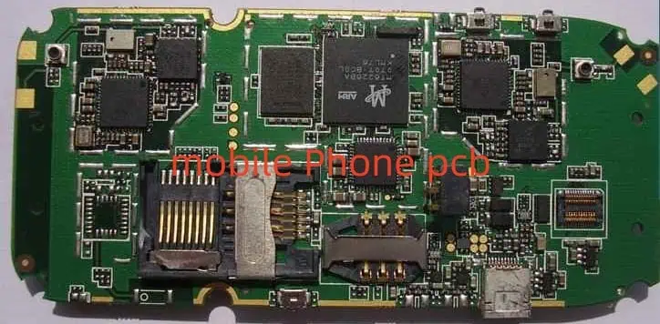
This board base housing surface-mounted as well as socketed components present in majority of electronics is called the home electronics PCB.
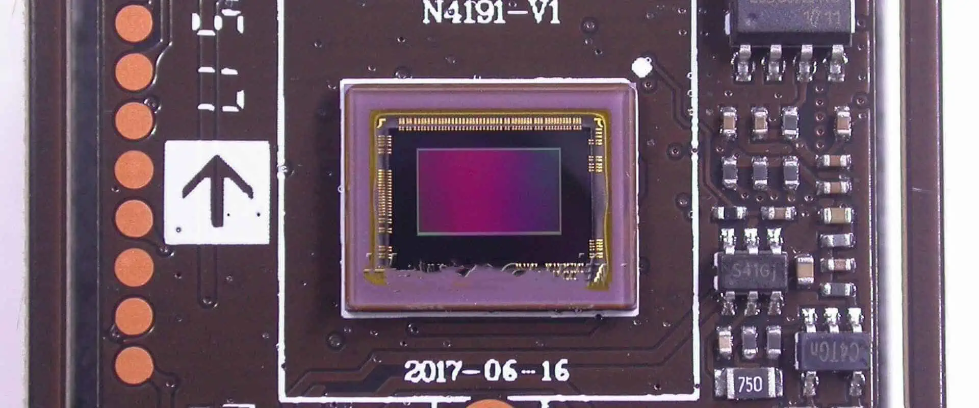
PCBs are created using a photolithographic method, which is a scaled-up replica of how conductive routes in the processors are created, for use in applications that require delicate conductive traces, like computers.
Using conductive paths, tracks, and signal traces that are etched from sheet layers of copper laminated to a substrate (non-conductive), home electronic circuit boards are employed to mechanically offer support as well as electrically link the electronic components.

Also, it is appropriately called the PWB (printed wiring board) as well as etched wire board when the circuit board contains just copper tracks as well as features but no circuit components like resistors, capacitors, as well as active devices which have been produced in the board’s actual substrate.
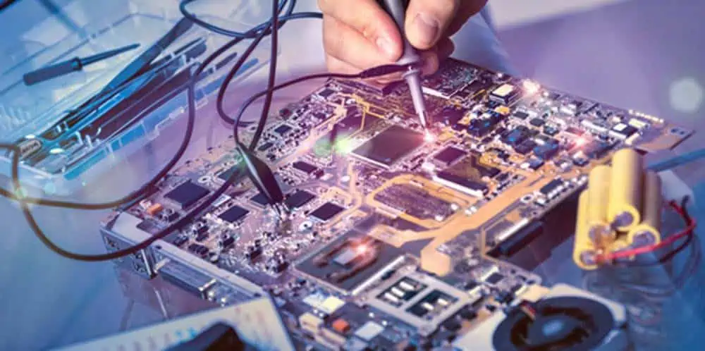
On the finished PCB with solder dabs already in place, household electronic components were normally assembled by a machine.
In the industrial oven, the circuit board bakes to melt all solder joining the connections. The majority of PCBs are constructed with the copper traces from glass-reinforced or fiberglass polymers.
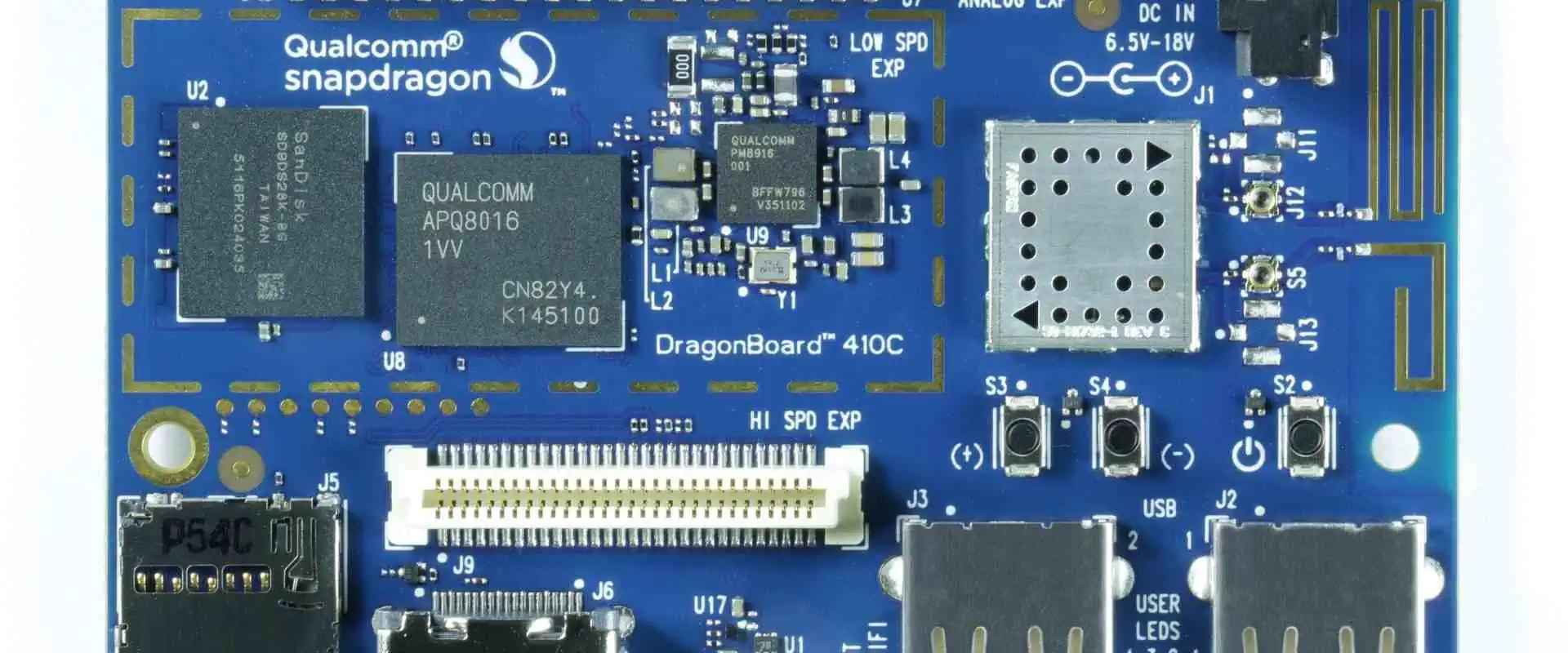
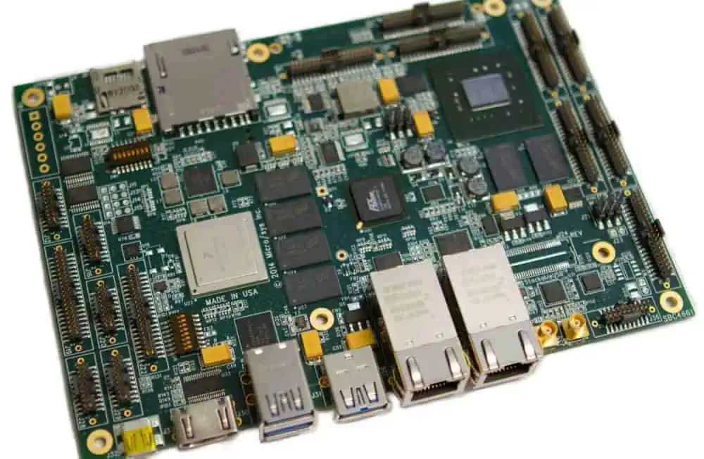
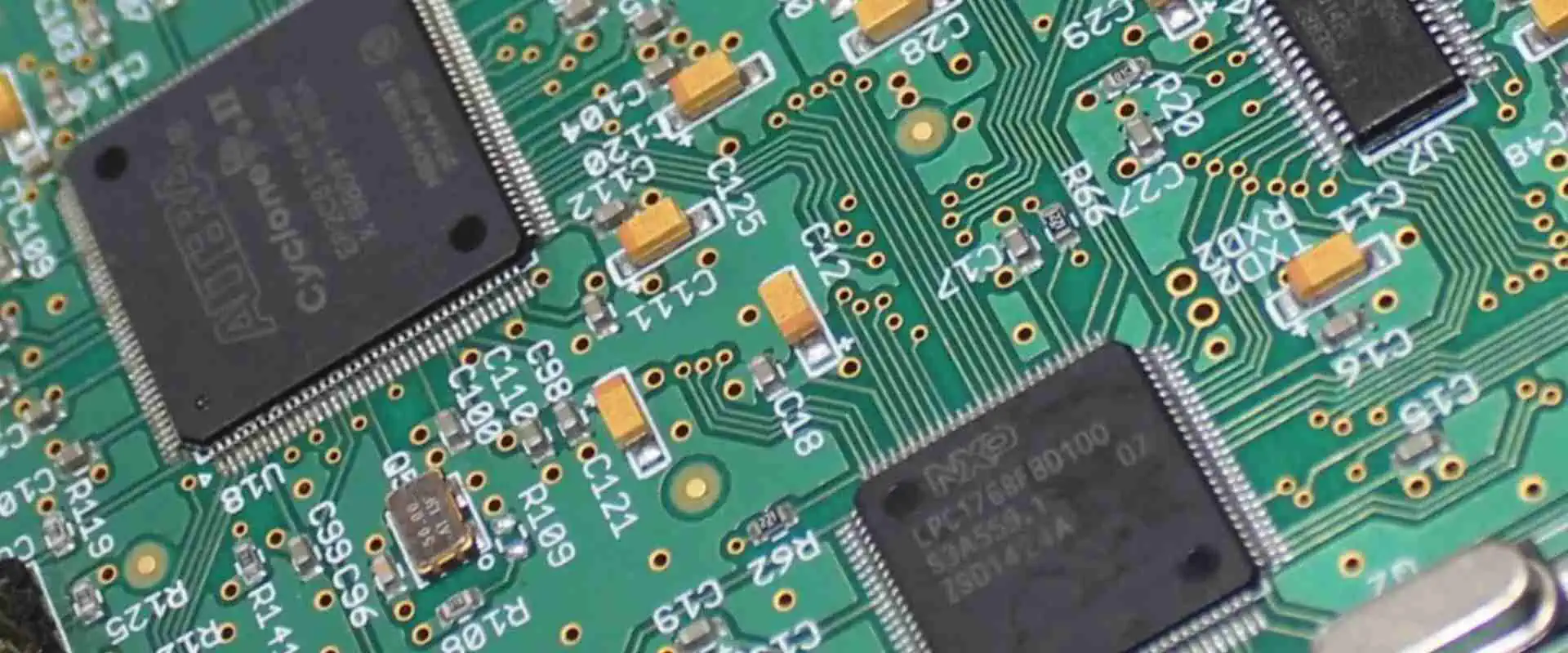
For a simple electronic device, single-layer PCBs are an option. Circuit boards with sophisticated hardware, like motherboards as well as graphics cards, can contain up to about twelve layers. The PCBs can be any color, although they are most frequently green. Silk-screening as well as CNC machining are additional techniques for producing PCBs.
Home Electronics PCB Applications
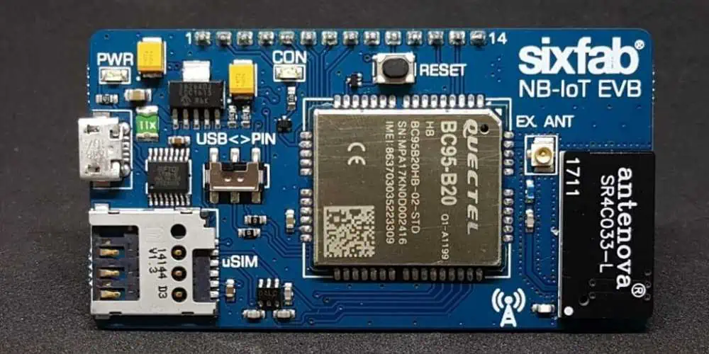
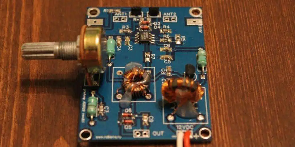
PCBs for home electronics have several uses in the production of consumer goods. When constructing, double, single, as well as multi-layered circuit boards are used for things like music systems, systems for air conditioners, microwave ovens, washing machines, remote controls for TV, lighting fixtures, vacuum cleaners, water boilers, digital wristwatches, alarm systems for home, coffee bots, CD Players, electronic toys that work with remote, video games (hand held), cable television, as well as home theatres.
Types of Substrate Materials for Home Electronics PCB

The materials used to manufacture PCBs are crucial because they must have exceptional qualities and features, including temperature resistance, adhesion, flexibility, tensile strength, dielectric strength, and dielectric constant. The materials utilized in the building of the substrates have a direct impact on the performance, dependability, and durability of home electronics PCB.
FR-2
The substrate type with the least performance is likely FR-2. In spite of being flame retardant (FR-2 stands for Flame Retardant of Level 2), phenolic substance, which refers to a specific kind of an impregnated paper put on the top of the glass fiber, makes up FR-2. These days, only a few extremely cost-effective consumer applications—like tiny, affordable radios—use this substrate.
FR-4
It is the substance that is utilized to make PCB substrates the most frequently. It is made of a laminate sheet of epoxy with glass reinforcement. That epoxy resin utilized is FR-4, or Flame Retardant 4th Level, and it is both water resistant as well as moisture-resistant. Its electrical insulation, strength/weight ratio, and tensile strength are all extremely high. Asides from the above-mentioned common traits, there are many varieties of FR-4 that differ in certain specific qualities.
PTFE (Teflon)
It is exclusively utilized in applications involving high speed as well as high frequency communications since PTFE, a form of plastic, provides no resistance. Due to its exceptional flexibility and high level of insulation, PTFE is useful in applications requiring precise tolerances.
Additionally, it has a high degree of mechanical strength, is flame-resistant, and retains its stable properties as its temperature changes. It is employed in different electronic devices which handles signals from hundred MHz down to ten GHz because of its super high-frequency properties.
Metal substrates
Aluminum-based metal substrates generally have strong thermal and dielectric characteristics and exhibit moderate expansion. Ultra – high frequency performance is guaranteed by aluminum, which can easily resist temperatures that reach 350°C.
This ceramic substrate, which is generated using an electrochemical technique that directly deposits an aluminum oxide crystal dielectric layer on an aluminum substrate’s surface, is electrically connected and coupled to that same aluminum substrate.
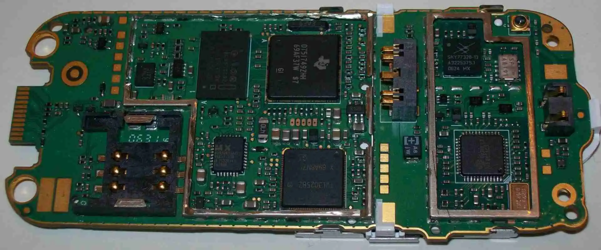
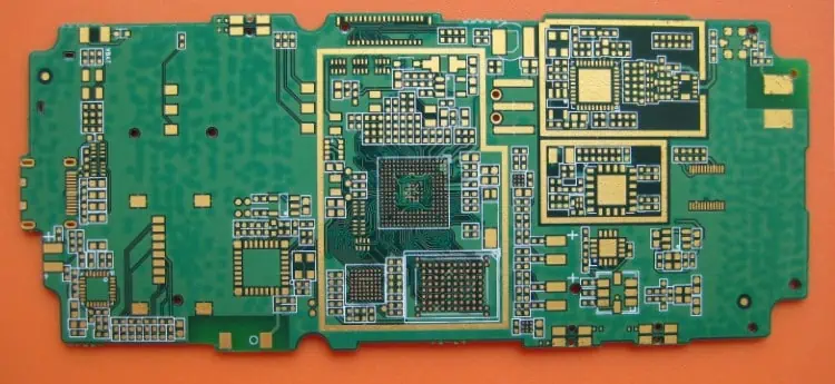
Types of PCB Used in Consumer Electronics

PCBs are widely used in electronics nowadays. They come in multilayer, double-sided, or single- double-sided varieties. They may be composed of both flexible and rigid elements or be entirely flexible or rigid.
The majority of people utilize them on a daily basis without ever realizing it, while they are essential to the electronics in use by numerous sectors. Three different types of circuit boards are used in the production of consumer goods and household appliances. There are three main ways to make PCBs:
Single layer
All of the electrical components come mounted on a side of a single substrate in single-layered Circuit boards, with its copper trace installed on the opposite side.
Double Layers
This type of PCB has two substrates, as its name suggests. Two sides of this substrate are fixed with components and parts.
Multi Layers
Typically, PCBs of this kind are employed in incredibly complex electrical circuits. These are constructed using a number of substrate layers that are separated via insulation. A PCB can contain about 42 layers, depending on how complicated the applications are.
Factors that Determine a Reliable Home Electronics PCB

High-grade base materials
The ability of this board to be able to conduct electrons flow is a clear indicator of a PCB’s reliability. If this base material is top notch, this capacity comes feasible. A high-quality base material for printed circuit boards can help prevent issues like open circuits and delamination brought on by inflation, among others. So, before being used, foundation material should be checked.
PCBs without track cuts
If no repairs of any sort are made using soldering and no break lines are repaired, a highly dependable circuit board could be produced. No maintenance is necessary for repairs made without soldering. Additionally, it prevents any error-related situations, giving PCB nearly flawless performance. Due to the lack of line breaks that need to be repaired, the likelihood of a break in current flow is virtually nonexistent. Circuit boards without soldering repairs are therefore thought to be very trustworthy.
Copper clad
Copper cladding on a PCB with high reliability satisfies the tolerance requirements outlined in IPC4101 quality criteria. For better control of the thickness of the dielectric layer, this is crucial. A dielectric layer that is thick aids in minimizing the deviation seen in the expected performance value.
Because copper cladding by itself can’t fulfill the task, attention is also devoted to the components’ quality.
Procedures for treating PCB
Even treatments applied during PCB manufacture don’t last forever. Therefore, it’s crucial to make sure the circuit board’s surface treatment hasn’t undergone any metallurgical changes when it’s being used. For this reason, before being used, circuit boards must pass a number of rigorous quality checks.
Advantages of PCB for Home Electronics
The utilization of circuit boards has numerous advantages. The primary benefit is they make items more portable and smaller.
Takes up less space
You can achieve a considerably smaller finished product since the circuits present on the home electronics PCB can sometimes occupy far less space compared to the individual components do. Additionally, this makes it simpler to assemble various components of the circuit as well as route traces in the appropriate directions.
Reliable and lasting
They are also incredibly strong and long-lasting. Also, they can withstand a great deal of harm, including heat, wetness, and physical force, ensuring it doesn’t disintegrate. This is what makes them perfect for usage in environments that are dangerous for electronics, such as the area under a car’s hood where they get exposed to substances like water and oil.
It is essential to allow the circuit boards to endure these conditions to ensure that it continues to function effectively, especially when it has to do with something critical such as braking systems.
Safety is ensured
A PCB’s circuits are enclosed, making it nearly impossible to contact two connections simultaneously with naked skin. By doing this, you have no risk of receiving electric shocks from your gadget.
Easy to recycle and repair
PCBs are simple to recycle and repair. In most cases, it is significantly simpler to repair a board-level component failure than it would be if it occurred elsewhere within the circuit. Additionally, recycling the board whenever it inevitably reaches its end of useful life won’t have any detrimental effects on the environment.
Conclusion
Since their debut in early 1990s, PCBs have advanced significantly. PCBs can now be produced by manufacturers to a variety of standards. They have cutting-edge production as well as testing systems.