Top 8 IoT Development Services

Apa Itu IoT

Connected devices are now more integrated than consumer products in smart homes. The increasing user integration is great for the Internet of Things. However, an exciting aspect of IoT is how it impacts companies across several industries.

The Internet of Things (IoT) is indeed a game-changer for organizations. IoT has transformed the activities and productivity of organizations. Also, connected enterprises can now compete against new and existing competitors. They can as well discover additional revenue opportunities, and optimize their efficiency. Therefore, this helps these enterprises to remain relevant in their given fields.

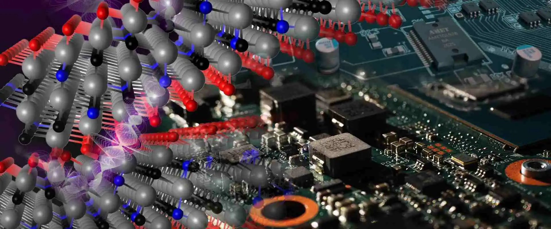
What is IoT Development?

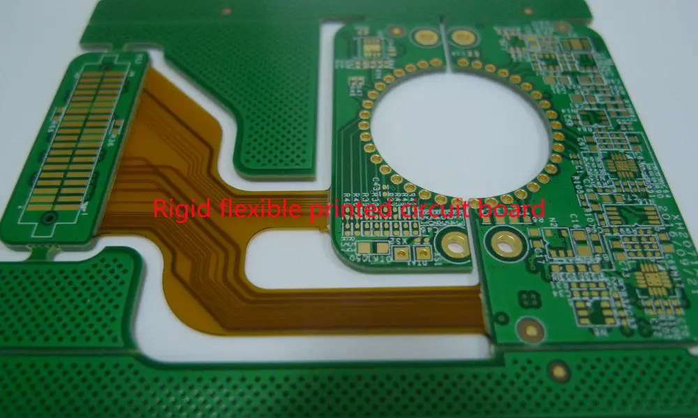
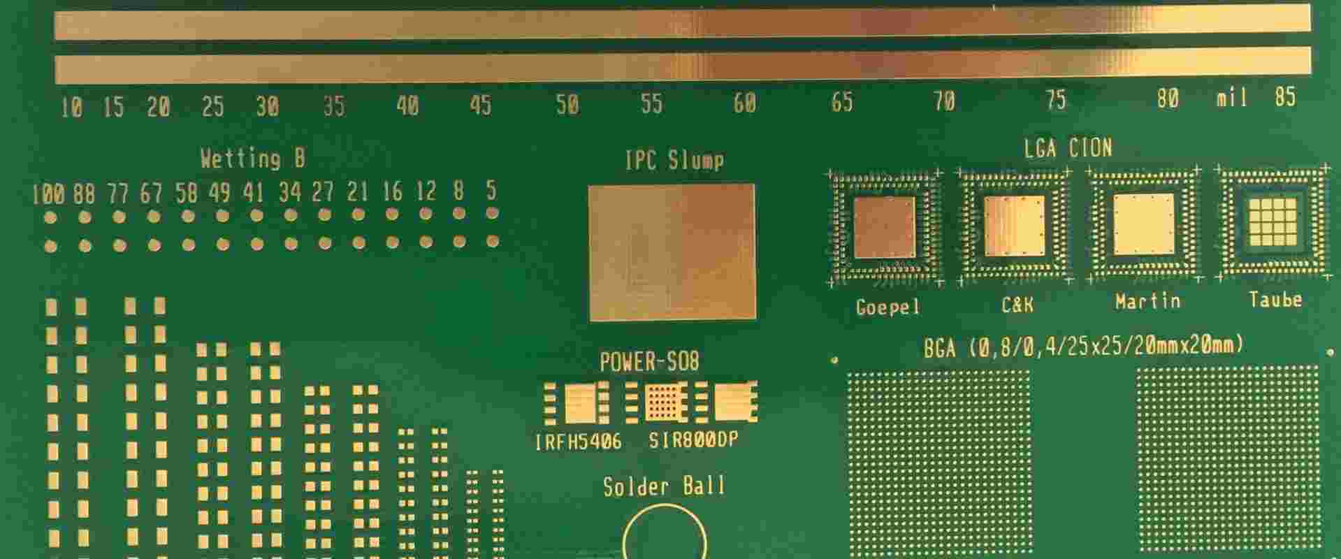
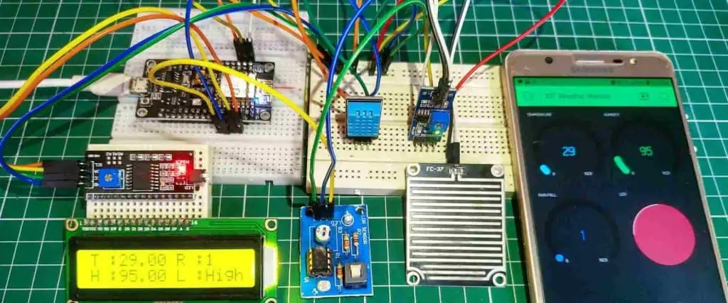
IoT offers businesses and individuals the possibility to integrate several devices utilized in various processes in a common computer network. Regardless of the application, IoT can enhance workflows, obtain data about the performance of devices, and more. However, to optimize the benefits of these systems, there is a need to invest in IoT development. IoT development involves combining hardware development with software development.

There are three consecutive stages in IoT product delivery. This includes integrating the software and device with the whole work environment, testing device connections and functions, and adapting prototype to industrial manufacturing.

The complexity of a project determines IoT development cost. The IT company will account for the team members selected for the project and hourly rate to calculate cost. Also, the billing method may be based on Fixed Price or Time & Material based on your company of choice.

ย 
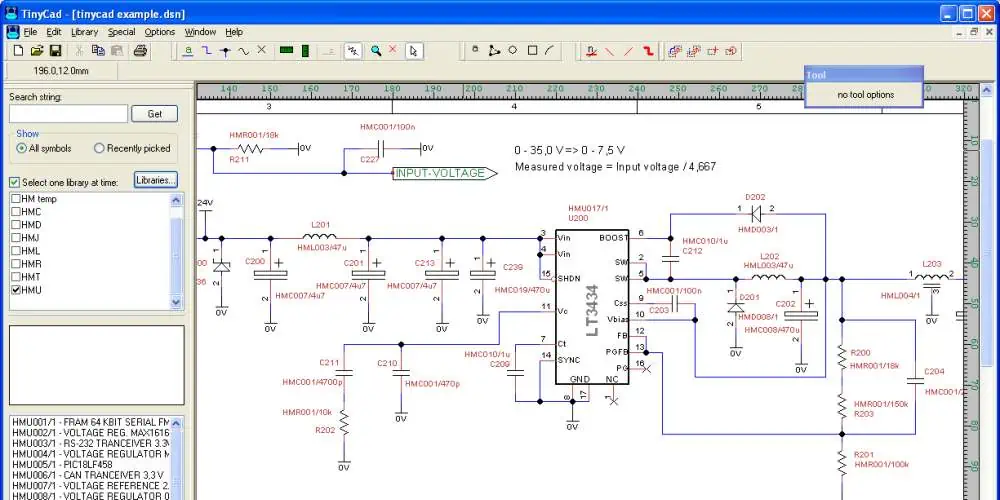
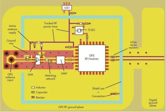
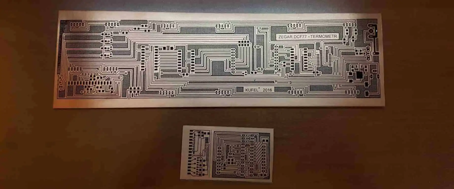
IoT development is a broad scope as it cuts across several aspects such as systems engineering, security, cloud programming, networking, hardware device programming and more. Therefore, IoT development ย involves collaborating with different professionals in the IoT development field implement and maintain IoT solutions.

Top IoT Development Services

Arduino IOT

Intellias Global Technology Partner

Intellias collaborate with IoT providers in the several industries ranging from automotive to real estate and transportation. This helps them to discover the business value of connected devices. Also, Intellia offers reliable IoT development services. Their team of experts helps organizations integrate the appropriate IoT technology stack to create data-rich software solutions for personal devices, connected vehicles, industrial purposes, and smart facilities.

Intellias offers various IoT projects which range from connectivity and embedded solutions to intensive platforms which are backed by AI-based analytics. Also, they offer customized IoT development services that allow organizations to optimize their operational efficiency and establish processes. These services  offer a high level of visibility over departments by using IoT apps, cloud services, and mobile devices, in a well-connected ecosystem designed around end users.

With Intelliaโ€™s extensive AI skillset, clients can unlock the full capabilities of real-time data to produce credible predictions.

ScienceSoft

With more than 11 years of experience in IoT software development, Science Softโ€™s IoT development services helps businesses to optimize their productivity. Their development services offer great IoT solution that improves work safety. Also, ScienceSoft offers IoT solutions for various use cases in more than 30 industries.

This IoT development company integrates a modular IoT architecture that offers fast horizontal and vertical scale up. Furthermore, ScienceSoft has a quality management system that is ISO 9001-certified. This system focuses o meeting the budget and quality expectations of customers. Also, they have a full-scale PMO which helps in handling complex and large IoT projects.

ScienceSoft has great experience in IoT development and an advanced approach to IoT project management. Therefore, this company will offer an efficient IoT solution while making their services affordable. They integrate quality skills with great knowledge about IT technologies. The team at ScienceSoft has continued to demonstrate a proactive approach to work.

STARTECH UP

STARTECH UP offers comprehensive IoT development services that help businesses leverage the power of IoT development and as well grow their competitive advantages. Also, this company has great expertise required to handle your IoT development needs. STARTECH UP works with back-end engineers, IoT specialists, professional analysts and consultants, front-end developers, and full-stack experts to offer the best IoT development services.

Before any development work commences, STARTECH UP ensures their consultants and analysts consider your business needs and tech ecosystem. Also, their professional engineers configure IoT devices and carry out live monitoring to enhance IoT deployment.

This company uses the power of IoT data to provide solutions to problems and uncover opportunities in the IoT eco space. Also, STARTECH UP designs and develops advanced processing environment that can handle complex data. This company offers their clients guaranteed success due to their comprehensive knowledge of IoT.

KiwiTech

FULL PCB MANUFACTURING Quote

KiwiTech helps businesses to manage, leverage, and control connected devices across a wide range application to improve your digital transformation. This company is highly preferred among some leading corporations and startups. KiwiTech understands that IoT spans across connectivity. Therefore, this company provides services that span across the whole lifecycle of initiatives associated with IoT.

Employees at KiwiTech apply their technology and design skills to help client succeed. Kiwitech offers IoT service offerings such as data retrieval, big data analysis, IoT platform integration, data processing and more. Also, they offer IoT development services for wearables. Compliance to industry-specific regulations and standards is one of the factors that distinguish KiwiTech from other IoT development companies.

Also, this company believes connectivity is much needed for IoT applications. Therefore, it ensures a stress-free experience by allowing clients to select the appropriate networking protocol. At Kiwitech, the team of professionals eliminates risks and integrates quality assurance approach to enable quick time-to-market.

INTEGRA SOURCES

This custom IoT development provider works with business and IT leaders on integrating internet-connected devices. INTEGRA SOURCES integrate data analysis and cloud computing by Mircosoft and Amazon to build IoT applications. Also, this company achieves great IoT projects by getting a compatible technology that works well with your IoT solution.

When you partner with INTEGRA SOURCES, you will enjoy several benefits ranging from diverse connectivity, effective data management, powerful analytics, safe data collection, and more.  Also, this IoT development company works with proficient designers and professional developers who create interactive and intuitive IoT applications.

In order to ensure optimal efficiency and functionality, this company adheres to certain standards and regulations in the IoT field.

Digiteum

Arduino IOT

Digiteum provides a wide array of IoT development services that ranges from IoT data pipeline architecture to developing mobile applications. Also, this company can bring life to your IoT project. The team at Digiteum has great expertise in creating interfaces across voice, web, and mobile. Also, this company can develop function web and mobile applications.

If you need an IoT development company to work with, Digiteum is the right option. This company will help their clients to strike a balance between uniqueness and functionality. With their broad experience and great technical skills in IoT software development, this company has continued to offer reliable services.

The team of professional engineers and developers in this company study the most recent platforms and frameworks for IoT development. Also, they are always available to choose cost-effective tools for their customers. Digiteum provides IoT software development services for smart cities, smart homes, and smart building. This company offer data solutions that help them understand how people integrate devices and spaces to improve the safety of smart cities and homes.

SoftwareHut

SoftwareHut works with more than 200 professional software engineers that focus on delivering IoT solution. This IoT development company is aware of IoT domination in our offices, homes, and lives. Therefore, SoftwareHut puts usability and functionality in mind. This IoT development company knows its craft when it comes to IoT software development.

SoftwareHut has always demonstrated their agility. Their team of developers focuses on delivering well-crafted IoT development solutions. Also, this team has what it takes to handle any model you need. At SoftwareHut, their main priority is to deliver high-quality software to their clients in a timely manner. This IoT development company has built a strong reputation for exceeding the expectations of their customers.

Also, SoftwareHut understands that businesses operate in a different way and as such, offers various engagement models. This company offers you nothing but the best.

Damco Solutions

IoT Monitoring

Damco Solutions helps companies integrate the power of connected technologies. Also, this IOT development company integrate machine learning, advanced analytics, and sensor data to develop scalable IoT platforms that manage machines. Damco provides end-to-end IoT offering s which includes edge computing, analytics, and sensors.

All of these offerings help to enhance operational efficiency and as well detect high business value. With their IoT gateway development integrates several protocols and devices. Damco Solutions enable businesses to connect their controllers, sensors, and smart devices to the cloud. Therefore, this helps them remain competitive.

Their IoT integration services understand the certain requirements and ensures your IoT project is well executed. With Damco Solutionsโ€™ expertise in IoT development service, clients are certain about quality. Also, this IoT development company prides itself in developing scalable and efficient IoT-driven applications.

Conclusion

IoT development plays a crucial role in the performance of IoT devices and applications. However, IoT development is usually executed by professional IoT developers. IoT developers develop, design, and manage IoT systems and devices by integrating research, technology, and data. There are several IoT development companies.

Everything you Need to Know about Low-Frequency EMI Shielding

If signal and radio waves were tangible and visible, then you would not move from around your own home without tripping on one of them. That is because signals and radio waves are literally emitted by most electrical gadgets, from smartphones to radios and laptops. But what exactly keeps these signals from effectively crossing? How come you answer a phone call via your smartphone near a computer, and the signal in your phone doesn’t disrupt the wifi connection on your PC?

The disruptions we are talking about are known as EMI or Electromagnetic interference. However, you do not experience disruptions due to EMI quite often due to the utilization of effective EMI shielding that manufacturers are now utilizing on most electrical gadgets. However, these shields come in multiple varieties, but we are going to look at one crucial type. The Low-Frequency EMI shielding. What is Low-Frequency EMI shielding? How does it function? Which components are utilized to make this EMI shield? And why is it crucial to gadgets that run on low frequency?

EMI in a Nutshell

low-frequency EMI shielding

EMI or electromagnetic interference occurs when one source effectively disrupts the signal of another source. In most cases, these sources are usually in close proximity. For example, if a smartphone receives a phone call while placed next to a radio, you might hear a crackly sound turn up on the radio, and then it goes back to normal after a while. However, at this moment, the signal from the smartphone temporarily disrupted the radio’s signal causing it to act abnormally.

EMI also goes by the name RFI (radio frequency interference). And while the example above simply states a simple example EM interference on a particular scale can cause more drastic effects than just making you miss some lines from a radio presenter.

Specifically, EMI impacts the electrical circuit of a device via induction, conduction, or coupling. What that means is that EMI can either make the electrical gadget function abnormally or make it fail.

Types of Electromagnetic Interference

There are only two types of electromagnetic interference, namely:

  • Narrow-band
  • Broadband

Narrow-band EMI

Narrow-band electromagnetic interference typically affects mobile phones, television stations, and radios. That is because this interference tends to happen over discrete frequencies. When this interference occurs, radio signals cross, causing the device to malfunction.

Broadband Electromagnetic Interference

FULL PCB MANUFACTURING Quote

Broadband interference tends to occur over a wider spectrum because it occupies a massive section of the EM spectrum. Moreover, broadband electromagnetic interference is powerful and can cause immense damage to electrical gadgets compared to narrow-brand EMI.

However, this type of EMI primarily affects gadgets that have digital data links.

Simple things such as worn brushes on a gadget’s motor can effectively cause EMI. Moreover, fluorescent lights that are defective can also cause EMI.

When drivers start their cars, they cause EMI via the ignition process. Moreover, EMI can come from a jet engine igniter, defective power lines, and much more. Therefore, EMI is hard to avoid.

In each of these examples, the gadgets you are attempting to utilize might receive varying transmitted frequencies. After receiving them, the device mixes them up, then sends them over a broad spectrum.

In the EM spectrum, radio frequency interference is at the top of the list of the most common types of interference. The energy that is radiated by engines, motors, lamps, lighting, power lines, and circuits causes this particular type of interference.

You might notice electromagnetic interference at home whenever your gadget fails to function as it is supposed to function. The same case applies to when you are at work. However, in commercial environments, this interference can cause wasted productivity, loss of data, and ruined hardware.

Low-Frequency EMI

Unlike high-frequency electromagnetic interference, low-frequency electromagnetic interference is pretty challenging to restrict from hitting sensitive circuitry. Therefore, this type of interference can easily reach power frequency levels or even go lower which could cause more problems.

As the EM wave’s frequency goes down, the absorption losses and reflection decrease while the strength of the field increases. Therefore, if you are generating a design for an EMI filter meant for low-frequency electromagnetic interference mitigation, you must make the inductor’s size pretty large. Moreover, considering all the variables at play, you must consider unique EMI shielding methods specific to low-frequency EMI shielding.

 Low-Frequency Electromagnetic Interference Shielding

As the name dictates, low-frequency electromagnetic shielding refers to the methods utilized to effectively block low-frequency electromagnetic signals from disrupting the circuits of electrical devices. To achieve this feat, manufacturers have to utilize enclosures that are made out of conductive components. The components that manufacturers select usually have impeccable permeability, which helps them divert the EM fields from the gadget of interest.

Low-Frequency electromagnetic shielding is pretty effective as per reducing the EM field’s strength. On average, these shields cut the EM field’s strength by about 95%. And considering the size and cost of the shield, it is without a doubt the most suitable solution to this problem.

Materials Utilized to generate EMI Shields

EMI-shield-PCB

Typically, at lower frequencies, the strength of the magnetic and electric fields tends to be pretty high. Therefore, manufacturers must utilize highly permeable components to achieve low-frequency electromagnetic shielding. Moreover, the materials that they select mainly depend upon the following:

  • EM fieldโ€™s strength
  • EM fieldโ€™s frequency

Low-frequency, electromagnetic shielding components are primarily selected to effectively block or alter unwanted EM fields from disrupting sensitive gadgets. Typical components utilized for electromagnetic shielding are:

  • Aluminum
  • Copper

These are impeccable components that have low reluctance and high permeability, making them perfect for low-frequency EMI shielding.

Other components utilized for low-frequency electromagnetic shielding include:

  • Steel or mu-metal

As per low-frequency EMI shield design, you can utilize online resources that give you multiple tools.

Conclusion

The production process of various EMI shields is different according to the application areas of the shield. However, all EMI shields do one particular job, block off EM fields from disrupting the electrical signal of electronic devices. However, the shield level varies according to the type of EMI the shield is trying to shield the gadget from. First, we have high-frequency EMI shields, which shield the gadget from high-frequency EMIs. Then we have the low-frequency EMIs that shield the gadget from low-frequency EMIs. We hope this article has provided you with all the answers you were looking for regarding low-frequency EMI shielding and why it is crucial to electronic gadgets.

What are the Necessary Files for Creating Rigid Flex PCB Quotes?

Flex Board Design and Rigid-Flex DesignFlex Board Design and Rigid-Flex Design

Circuit boards that combine rigid and flexible board technologies are known as rigid flex boards. Depending on the application’s design, the majority of rigid flex boards are made up of many flexible circuit substrate layers that are outwardly or internally attached to at least one rigid board.

These flexible substrates often are molded into a flexed curve while installing or manufacturing and are intended to remain in a state of constant flexibility.

RAYMING 10 Layer 2 step HDI Rigid-Flex PCB Boards

RAYMING 10 Layer 2 step HDI Rigid-Flex PCB Boards

Original price was: $2,580.00.Current price is: $2,560.00.

Product name: 10-layer 2-step HDI rigid-flex boards Board Material๏ผšTaiguang EM-888S Thickness: 1.0mm Number of layers๏ผš10 layers PCB Minimum line width/spacing: 4/4mil Finished copper thickness: inner layer 0.5OZ, outer layer 1OZ Acceptance standard: IPC6012 CLASS 3 level Surface technology: immersion gold Dielectric constant: 3.8 Loss factor: 0.0055 Usage: Security monitoring equipment

What are Rigid Flex PCB Quotes?

Finding a producer to produce the design after it has been prepared by the designer of the rigid flex board is the following stage. To order the board, you must provide an estimate as well as PCB quote.

The main objective is to build and assemble the rigid flex boards using the fewest procedures and at the lowest cost.

A manufacturer can only provide a precise quotation if your PCB designer provides all the relevant details. Let’s examine some important information that is occasionally forgotten while acquiring a quote.

The rigid flex PCB quotes is a general estimation of the manufacturer’s capacity to produce a design for your rigid flex PCB into the physical board in terms of cost, time, and other factors. It isn’t necessarily connected to the design of the board. A quote can be requested for information regarding PCB design, production, or assembly.

How to Create Rigid Flex PCB Quotes

It’s more than a cost estimate for the required quantity of pcbs, rigid flex PCB quotes from your CM also includes an estimation of your fabricator’s time requirements and capacity to incorporate all the technologies present in your board design.

The accuracy of this quote facilitates the process of production. To expedite the process and prevent delays, it is advisable to supply all pertinent information at once. In the event that any vital details are absent, the CM must get in touch with the designer. While we are having this conversation, the purchase must be put on hold. An order may miss the deadlines for internal manufacturing if it is kept on hold for an extended period of time.

It’s possible this will cause the manufacture to take a much longer time than anticipated.

The crucial details required for precise rigid flex PCB quotes are as follows:

  • The board type (rigid-flex, flex, rigid, etc)
  • Board layers in total
  • Each boardโ€™s dimension
  • The holeโ€™s minimum diameter
  • Material
  • Minimum trace width
  • Trace spacing has to be kept at a minimum
  • Outer layerโ€™s copper finish
  • Annular ringโ€™s requirements
  • The holes in total

How to Make Rigid Flex PCB Design Quotes

FULL PCB MANUFACTURING Quote

A quote on PCB design (layout and schematic) is asked whenever the requestor is unable to create a layout and does not have the necessary resources.

The most important files provided are often schematic, BOM, board layout, as well as mechanical information. The requirements for the design must also be stated. A quotation for the design service will include the price of the circuit board as well as the expected time period.

The following results are anticipated from Circuit design services:

Choosing a design tool

Users can choose from a range of design tools that CMs offer. The selected tool will be used to produce the schematic as well as all files related to the design.

Schematic

You can submit a rough schematic with your request for a quote, and their design staff will transform it into the desired CAD format.

Reducing costs

In order to reduce costs and increase process effectiveness, the manufacturer would find a means to get around the specified design.

Reversal Engineering

Some CMs will create all the files for the design for a fresh PCB utilizing the specifications of the existing board. This depends on the situation. These specifics could come from the board that is empty or filled, or even only from drawings or design files. Files for the new design will be made due to the designer defining the differences out from prior board.

Files Needed for Rigid Flex PCB Quotes

rigid flex pcb design guidelines

The necessary files are required for the rigid flex PCB quotes. A fabrication quote requires these files:

Upload a Gerber file having English units in ODB++ or RS-274X format. These files ought to be produced for each surface of the circuit board.

The fabrication print as well as design, including the board shape, the drill pattern, as well as the hole diameters (in the Gerber format).

  • A outstanding drill file in ASCII format comprises data such as tool units, units, coordinates, and number format.
  • A readme.txt folder contains details about the board, the files, and the layer stack-up.
  • IPC netlist that shows the list of network that identifies the connection system for conductivity on the circuit board.

Documents Needed for Rigid Flex PCB Quotes

What is required to obtain a PCB quotation? This is a great question that usually leads to miscommunication. There really are four core documents, and the way they are transmitted depends on the technologies used by your firm; we can work together to find the best option for you.

We will go over which documents are necessary, what details they all should have, as well as how they relate to the quote procedure.

Here are the mandatory paperwork:

Bare-Board Print

The print, sometimes referred as the fab drawing or fabrication drawing, gives us the necessary documents to build the bare PCB. the board’s material, thickness, finish, the holes as well as the smallest hole size required, the number of layer needed, and the color of the solder mask.

Assembly printing

It essentially serves as the blueprint of the manufacturer and identifies the locations of each component in addition to any special packaging or markings demands for the single circuit board.

Bill of Material

The document which controls the components is the BOM or bill of material.  Every line item present on this BOM needs to have a description, part number, quantity, as well as the reference identifier.

Conclusion

The accuracy of a quote facilitates the process of production. To expedite the process and prevent delays, it is best to submit all pertinent information precisely.

What is the Difference Between Non functional Testing and Functional Testing?

Assembly Testing

What comes to mind first when you consider software testing? Integration tests and unit tests are frequently on the minds of many engineers. A codebase with a top-quality manufacturing must be created and maintained using the two software testing techniques. However, they don’t serve all by themselves.

The testing procedure of your team should evaluate the complete application, take a broad look at the way it functions whenever it is working properly, and sound the alarms whenever deviations are discovered. A thorough software testing method must include both non-functional and functional testing to increase trust at every application tier.

What Does Functional Testing Mean?

aluminum pcb test

Functional testing is concerned with evaluating an application’s usability in light of some standards or requirements. Testing sections of an underlying code during functional testing is common.

Individual modules for testing in isolation does not give a clearer broader picture than comparing actual outputs to intended behaviors. Errors typically occur when modules interact with one another.

Functional testing comes in various forms, including:

  • Unit tests (which is also useful for non functional testing)
  • Testing for integration
  • Testing for user acceptance
  • Closed-box test

Unit tests

If a system is installed in any testing environment, the unit tests meant for the API application could send requests to it and then compare the results with the documentation. But there are only a few unit tests. Functional tests that cover the entire application frequently catch changes which unit tests miss whenever the application regresses or deviates in functionality.

Testing for integration

Software module integration testing verifies how they work together. The components depend on the explicit contracts in the way they interact when it is written by developers as loosely connected modules, as it typically should be.

Integration tests produce warnings whenever these interactions result in regressions as well as verify that each component of the product fulfills its contractual obligations.

Testing for user acceptance

The goal of the phase of user acceptance for software testing is to simulate real-world interactions as well as functionality by giving end users and otherwise their representatives access to some or all the program. Owing to its non-dependability, expense, and time commitment, testing for user acceptance is rarely significantly relied upon in healthy cultures for engineering. Nevertheless, some testing for user acceptance is an important step in the testing process for the majority of applications.

The Closed-box Testing

Here, the entire application is another type of functional testing that is possible. Closed-box testing ignores the application’s internal workings in favor of only testing the outputs of the application. When developing functional tests so as to complement the non functional tests, a lot of developers tend to gravitate towards it.

Only its output is examined; the code which interacts with its outermost layers gets automatically verified. For apps that only need API testing, this procedure is straightforward because the code just needs to make API calls as well as analyze the outcome.

Closed-box testing is becoming more challenging when used to apps having the user interface. Utilizing an advanced testing tool such as Selenium is one method of addressing this difficulty. With the assistance of these tools, code can communicate with such an application just like a user would in the web browser. User acceptability testing is automated with the help of Selenium and similar tools, which also improve reliability and scale. However, using closed-box testing for user interfaces is a difficult issue with particular difficulties. The engineering bandwidth of your team could be quickly depleted.

What Does Non Functional Testing Mean?

FULL PCB MANUFACTURING Quote

Non functional testing evaluates aspects of an application that don’t directly affect its functionality but are still important for the user experience. Although they aren’t functional parts of the software system, reliability and performance under stress can definitely break or make your user experience.

Non functional testing failures don’t always result in a problem that users would experience, but they can point to a larger systemic issue. Non functional testing come in a wide variety of forms.

Performance Testing

Performance is the focus of one crucial non-functional testing procedure. The software system is tested for performance to ensure it responds to queries quickly. Poor latency ruins the user experience, as well as a well-written tests for performance frequently find issues before users notice them.

Load testing

A comparable category of the non functional testing is load testing. Few systems can reply to a single request every second with the same speed as they can handle about 10,000 requests every second. A system’s ability to manage peak loads as well as fail gracefully whenever it doesn’t have the capability to handle the spikes in workload is verified through load testing.

Usability Testing

Testing for usability evaluates how well a user interacts with a product. Usability testing seems to be typically a manual technique which doesn’t scale effectively. However, the lack of the usability testing, particularly when localizing software, sometimes results in muddled and imprecise user interfaces. Integrating this kind of testing in the development process of your software is time well spent.

Security Testing

Another class of non functional testing is security testing. Your team must routinely test the applications to ensure that they are safe and the data is correctly handled.

Depending on how exposed an application is to potential attacks, security testing could range from routine penetration testing to automatic scanning. Many teams do not consider security testing to be a component of their testing arsenal. It is wise to incorporate security testing but also treat it with the same seriousness as the unit testing type.

Portability Testing

This software’s ability to run on many operating systems and not experience any bugs is tested for portability. The functionality of software running on the same operating systems but with different hardware is also tested here.

Accountability Testing

A test of accountability is conducted to see whether that system is functioning properly or not. Every function ought to produce the same outcome for which it was designed. If that system provides the expected output, then the test passes it, and otherwise, it fails.

Reliability Testing

The reliability test makes the assumption that a software system operates without error under the predetermined parameters. The required duration and quantity of processes to serve the system are specified. If this system fails under certain predetermined circumstances, the reliability test would also fail.

Efficiency Testing and Evaluation

An efficiency test looks at how many resources were used as well as how many were required to construct the software system. The evaluation of these three elements is also included.

  • A software system must meet the needs of the client
  • The software system must meet customer criteria
  • The software system must be developed with sufficient effort.

What are the Benefits of Non Functional Testing?

  • It offers a greater degree of security. This security forms a crucial component that keeps systems safe from online threats.
  • It guarantees the system’s loading capacity so that all users can utilize it at once
  • Also, it enhances the system’s performance.
  • Since test cases never are altered, they need only be written once.
  • When compared to some other testing techniques, there is a smaller overall time commitment.

Comparing Functional and the Non Functional Testing

Non functional tests verify that a code is performing the proper actions, while functional tests verify that such code is carrying out the proper actions. Methodologies enabling the validation of back-end and front-end behaviors and elements are present in both types. In terms of the types of tests the developer may run, there may be some overlap in-between both categories.

The issues that software solutions aim to address must be resolved. Non functional testing frequently refines only incidental implementation performance and details measures. These factors are also taken into consideration by a thorough testing process, especially when scaling is important.

Functional testing is frequently sluggish to execute and expensive to maintain and write. Because they provide test-driven construction and frequently result in self-documenting code, many developers place the greatest emphasis on the unit tests. Whenever the requirements for the code change, it is simple to adjust these tests and they can be run quickly. Closed-box testing, for example, requires a lot of time to execute and write even with contemporary tools including Selenium.

A thorough blend of functional as well as non functional testing is the testing strategy that is the most unbiased.

A “testing pyramid,” that instructs developers to write majority of the tests as a unit test because they are very fast to execute and write, is something that many developers adhere to.

Conclusion

As important as tests which verify functionality is non functional testing. Due to the improvements provided by non functional testing, it is not as significant, many teams give it lower priority. Also, users might not have been able to utilize the features that they require at all if functionality becomes broken. Functional tests are the cornerstone of many teams’ testing methods for software due to this, as well as quicker execution times but also reduced costs.

Nevertheless, non functional tests are important, and the team must work to include them. A top-notch testing suite would confirm a variety of non-functional traits and components, which includes usability and performance.

Make Your Dreams a Reality with Free Schematic Drawing Software

Online Circuit Diagram Maker

Are you an engineer, architect, or construction professional needing schematic drawing software? Look no further! With the help of free schematic drawing software, you can design and simulate components and systems such as transistors, resistors, capacitors, relays, and switches. You can also develop robotic systems and 3D models as well as layout printed circuit boards with the help of these software tools. The following article will dig deeper into the free schematic drawing software.

Free Schematic Drawing Software

Schematic drawing software is a powerful tool for anyone in the electrical engineering, architecture, or construction industries. It helps in creating detailed diagrams of circuits and systems for use in a variety of applications. Additionally, it’s also applicable in educational and hobbyist communities.

Applications of Free Schematic Drawing Software

free schematic drawing software

1. Circuit Design: Free schematic drawing software typically help in designing electrical circuits. It allows users to create and simulate various components and systems, such as transistors, resistors, capacitors, relays, and switches. Additionally, it helps users visualize the results of their circuit design, allowing them to identify any potential problems quickly.

2. Robotics: Free schematic drawing software help design robotic systems. It allows users to create detailed models of robots, including the parts and motors they use. It also allows users to simulate their designs to test the robots and their parts before manufacturing.

3. Computer-Aided Design: This software allows users to create 3D models of components and systems for further analysis and virtual testing. It is often helpful in engineering designs and simulations.

4. Electronics: It helps users visualize the electrical connections between components and check for any design errors or conflicts. In addition, it helps in troubleshooting electronic components and systems.

5. PCB Layout: Free schematic drawing software help in designing printed circuit boards (PCBs). It helps users lay out the components and connections on the board and check for any potential errors.

Top 5 Free Schematic Drawing Software

FULL PCB MANUFACTURING Quote

The following are five of the most popular free schematic drawing software:

1. EasyEda:

EasyEda is a powerful and easy-to-use online schematic drawing software tool. It enables users to quickly create and share schematic diagrams, PCB layout designs, and simulate circuits. The platform has various components and symbols users can use to design their circuits. It also features a real-time circuit simulator that helps simulate and troubleshoot the circuit.

Features

Here are some of the features of EasyEDA that make it stand out from other circuit design tools.

  1. Simple to use – EasyEDA offers a simple user interface that allows anyone to start creating circuits rapidly. The user interface is simple, allowing even people with modest circuit design knowledge to get up to speed quickly. It also provides an extensive component library and a variety of simulation tools.
  2. Circuit Simulation – EasyEDA provides a robust circuit simulator for testing and debugging designs before manufacturing. The simulator can test a circuit’s functionality and replicate its behavior under various scenarios. This feature allows designers to detect and correct mistakes more quickly and efficiently.
  3. PCB Design – Besides the entire PCB design module, EasyEDA also provides a PCB design module. It comes with various tools for designing and laying out printed circuit boards, including component placement, trace routing, and design for manufacturability. It also has a set of design principles that ensure that the layout adheres to industry standards.
  4. Collaboration – EasyEDA facilitates user collaboration. It enables users to share their designs and remark on one other’s work. This aspect allows for getting comments from other users and learning from each other’s designs.

2. CadSoft Eagle:

PCB Layout in KiCA
PCB Layout in KiCA

CadSoft Eagle is a powerful schematic drawing software for professional and hobbyist users. It allows users to create complex schematics and PCB designs easily.

Features

  1. Schematic Capture: CadSoft Eagle has a graphical editor for schematic capture that is simple to use and allows you to drag and drop components and wires to create your designs. You may also utilize the autorouter to link your components quickly and precisely.
  2. PCB Layout: CadSoft Eagle’s powerful layout editor allows you to create professional PCBs with up to 16 layers.
  3. Simulation: CadSoft Eagle has a robust simulation engine for testing and evaluating your ideas. You may model and examine your designs using the software’s wide range of tools.
  4. Library Management: CadSoft Eagle has an extensive library of components and symbols to help you quickly develop designs. The library manager allows you to organize, manage, and share libraries with others.
  5. Cross-Platform Compatibility: CadSoft Eagle is available for Windows, Mac OS X, and Linux so that you may work on your designs regardless of platform. CadSoft Eagle is also interoperable with a wide range of CAD and EDA tools, making it simple to share your designs with other users.

3. SmartDraw:

This is a powerful diagramming and schematic drawing software. It offers users drag-and-drop tools for creating a wide range of diagrams, including flowcharts, organizational charts, floor plans, and more. In addition, it comprises a library with over 7,000 symbols and images, which users can use to customize their diagrams.

Features of SmartDraw

  1. Straightforward Interface – SmartDraw is an intuitive interface that allows people with no prior design experience to produce professional-looking visuals quickly. The drag-and-drop functionality enables users to swiftly add and rearrange pieces to create unique designs, while a variety of pre-made templates serve as a starting point to get the task done faster.
  2. No Coding Required – SmartDraw eliminates the requirement for coding. Instead, people may concentrate on their ideas and quickly produce pictures. As a result, it is an excellent choice for people more interested in the creative side of design.
  3. Automated Drawing – SmartDraw employs automated drawing technologies to create visuals quickly and precisely. This feature ensures that users can generate images with precision and accuracy, saving time and effort.
  4. Customizable Templates – SmartDraw comes with various pre-made templates to get users started, but it also enables customization. This implies that users can design images personalized to their specific demands and represent their style.
  5. Versatile Output – SmartDraw can generate visuals in various formats, including SVG, PNG, and PDF. This feature makes it simple to exchange visuals across multiple platforms and devices. It also supports a variety of popular cloud storage services.

4. Circuit Lab:

Circuit Lab is a free schematic drafting and simulation application accessible from any internet-connected device. It’s ideal for students and amateurs who wish to experiment with electronics without buying specific software or hardware. Circuit Lab includes a component library and a real-time simulation engine that allows users to test their circuits and immediately view the results.

Features

Here are some of the features of Circuit Lab that make it an attractive choice for circuit design and simulation.

  1. Easy to Learn and Use Interface: Circuit Lab offers a simple-to-learn interface. Additionally, it provides a drag-and-drop feature for components, making the design process simple and easy. The graphical user interface has various valuable aspects, such as color-coded components, zoomable panels, and context-sensitive information. This makes it simple to create and simulate circuits rapidly and precisely.
  2. Simulation Tools: Circuit Lab includes several simulation tools that allow users to model the behavior of their circuits precisely. These techniques include DC Sweep, AC Sweep, Fourier Analysis, Transient Analysis, and PSpice. Moreover, these tools help examine a circuit’s performance and identify potential flaws or areas for improvement.
  3. Custom Components: Circuit Lab allows users to design custom components. This capability enables users to construct custom parts with unique attributes within the software. Consequently, users can develop custom components that may be helpful in various simulations. In addition, users can access a library of components that is helpful in a wide range of projects through this functionality.
  4. Advanced Analysis: Circuit Lab offers a variety of advanced analysis choices to users. These alternatives include circuit simulation, Monte Carlo analysis, and harmonic analysis. These advanced analysis features allow users to see how their circuits perform in various conditions. Consequently, users can better understand the behavior of their design and determine whether changes are needed to optimize it.

5. XCircuit:

XCircuit is an open-source schematic drawing software for Linux, macOS, and Windows operating systems. It is a versatile tool well-suited for various electronic design projects, including single-board circuits and complex systems. XCircuit is equipped with a comprehensive library of components, and it offers a range of drawing and simulation tools that make it easy to create and test circuits.

Features of XCircuit

RF PCB design layout
  1. Simulation: XCircuit includes a comprehensive simulation engine that allows users to simulate various circuits, including digital, analog, and mixed-signal circuits. This simulation engine precisely mimics the behavior of components and interconnects to give extensive analysis and visual feedback. The simulation engine also supports many third-party components and models, allowing users to simulate complex circuits efficiently.
  2. Analysis Tools: XCircuit contains several tools to assist users in analyzing and optimizing their designs. Among the features available are frequency domain analysis, transient analysis, time domain analysis, and optimization tools. Each of these qualities can aid in analyzing the circuit’s behavior and provide insight into how modifications to the design will affect the circuit’s performance.
  3. Documentation: XCircuit includes a comprehensive documentation package to assist users in understanding the software and its capabilities. This content includes tutorials, user guides, reference manuals, and other items. This documentation makes learning and comprehending the software and its capabilities straightforward for users.
  4. Support: XCircuit provides users with several support options. This functionality includes a customer care staff, a user forum, and an active user and developer community. This feature makes it easy for customers to get the help they need when they encounter problems or have questions about the product.

Conclusion

Free schematic sketching software is a powerful tool that professionals, amateurs, and students can use. It can help construct precise diagrams and models in fields ranging from circuit design to robotics, computer-aided design, and PCB design. EasyEda, CadSoft Eagle, SmartDraw, Circuit Lab, and XCircuit are all excellent examples of free schematic drafting software with various features and capabilities. With their simple interfaces and easy-to-use capabilities, these tools take the complexity out of circuit design, allowing anyone to develop and simulate complex circuits.

What Service Does the Embedded Hardware Engineer Offer?

Embedded Hardware Engineer

“What does the embedded hardware engineer do?” is a common question I get from people from outside industry as someone who works in the embedded sector. I therefore wrote this piece to respond to that query.

What service does the embedded hardware engineers do? The primary responsibilities of the embedded hardware engineer include component selection, PCB design, hardware testing, creation of specialized testing tools, and design of other associated hardware such as product casing and test benches, and a small amount of production software programming.

In the parts that follow, we’ll look more closely at the aforementioned activities, and then we’ll consider other topics related to an embedded hardware engineer.

Activities of the Embedded Hardware Engineer

Embedded Hardware

Let’s examine the above-mentioned activities in this subsection.

Choosing Components

This is usually the first thing done when beginning a brand-new project. The first step is to choose a microcontroller which will satisfy the project’s requirements. Then, based on a project’s needs, the necessary sensors are included in the list of parts. The circuitry of the power supply, ports such as HDMI, USB, and Ethernet, as well as the supporting circuitry must all be added after these primary components have been decided upon before the component listing is complete.

Development boards were typically utilized in combination with breadboards to create and test circuits after hardware has been chosen.

This circuit is afterwards transferred to PCBs. Additionally, the Software team is handed the development boards so they can get to work as Circuit board design and fabrication are typically time-consuming.

Designing PCBs

Designing PCBs is the following phase. All supporting circuitry, including the power supply, is designed in this step, and passive parts like capacitors, inductors, and resistors are included on the list. To simplify the process a bit, instructions for the circuitry are often accessible from the manufacturer’s datasheets and websites. The PCB design (not schematic) presents the biggest difficulty in this case. (For readers unfamiliar with the term “schematic,” it simply refers to the circuit diagram.)

PCB designing tools like KiCAD or Eagle are used to create the Circuit design. Once the PCB design is complete, several PCB manufacturers typically get an order. The time it takes to produce and deliver product to you can range from a few days to few weeks, depending upon the manufacturer. At this time, the required components are also bought online so they are prepared to begin assembly when the PCB does.

Setting up the board

Here is where well-known instruments like microscopes, multimeters, and soldering stations are employed. The first iteration of a hardware is created by soldering the components onto the Circuit board using the aforementioned techniques. This job requires good hand-eye coordination as well as some patience. With practice and time, you will definitely get better.

Designing and Handling Hardware Tests

FULL PCB MANUFACTURING Quote

The board is now put through some tests using JTAG in order to check for short and open circuits before being given to a software team. At this stage, software engineers will typically be also involved, and they will likely get some tests prepared to ensure that the hardware performs as intended. The board is then prepared to be given to a software team immediately these tests are finished.

Creating Additional Related Hardware Required For Manufacturing And Testing

The first step is ensuring the necessary adjustments based on test findings, the schematic, as well as the PCB designs now that the original development circuit boards are prepared and have been given to the software team. Typically, some changes will be required and the PCB designs and schematic will be more refined.

Additional gear, such as test benches as well as use case simulator, will be required in addition to the device for the software testing. Since these are internal tools that are not provided to end users, there is no need for miniaturization, which facilitates the design process for such tools.

Custom hardware might also be required so as to manufacture the device in large quantities, and this hardware is currently being built and tested. Additionally, some manufacturing software might well be required, which is also included.

These are regular tasks performed by embedded hardware engineers. Let’s examine the abilities required for the embedded hardware engineers to carry out the aforementioned tasks in the following part of this article.

What are the Skills Needed to be an Embedded Hardware Engineer?

embedded-components-in-pcb

The embedded hardware engineer has to possess the necessary knowledge regarding:

  • Reading schematics and datasheets
  • Electronics fundamentals
  • Circuit analysis and design
  • PCB design
  • Circuit debugging
  • Electrical engineering
  • JTAG for testing and production
  • Effective utilization of tools such as Oscilloscopes, Spectroscopes, and Multimeters
  • Soldering
  • Microcontroller architectures

These are merely the fundamentals; additional expertise, like as understanding of networking as well as radio engineering, may be required and learned according to the device being designed.

Frequently Asked Questions

What services does the embedded software engineer offer?

Software created by embedded software engineers operates on a variety of devices with specialized hardware, including Xbox controllers, monitors for blood pressure, smartwatches, bluetooth headphones, and microwave ovens. You can read a different piece about this that I wrote about at this website.

What do engineers who design PCBs do?

These professionals create high-performance Circuit boards with several layers in order to miniaturize products while maintaining their functionality. The PCB’s performance can be impacted by a variety of external conditions, including electromagnetic interference and temperature, the PCB designers’ job involves the offering of solutions to related problems, as well as design circuit boards which provides high performance.

Why work as a radio engineer?

These professionals are responsible for designing all the RF components of the device. They engage in impedance matching, resonant circuits, RF amplification, as well as filter design.

Conclusion

By now, you should understand what the embedded hardware engineer does. Their primary responsibilities include component selection, PCB design, hardware testing, creation of specialized testing tools, and design of other associated hardware such as product casing and test benches. Any questions? Please reach out!

What is the Significance of ENIG Plating Thickness?

ENIG PCB

PCBs are now a crucial component of different electronic circuits. The circuit boards must withstand the challenges of various operational conditions. As a result, such circuit boards were covered in a variety of surface treatments.

On a Circuit board, a layer of copper that comes into touch with air oxidizes. Thus, the soldering quality is diminished. Surface treatments improve electrical performance, solderability, and oxidation reduction. There are many different surface treatments on the market. One such significant variety, the ENIG surface finish, as well as the ENIG plating thickness will be the focus of this article.

What Does ENIG Plating Mean?

A surface coating known as ENIG referred to as Electroless Nickel Immersion Gold) can be used to cover copper pads present on circuit boards in order to prevent corrosion as well as other irregularities. This copper pad was initially covered with a layer of nickel (Ni), which is followed by one layer of immersion gold (thin Au). The circuit board’s great electrical performance is achieved by ENIG’s superior oxidation resistance, great surface planarity, and ease of soldering.

Even though ENIG is more expensive and complex than other PCB processes for plating like HASL, it complies with the RoHS standard and is one of the most popular circuit board surface finishes as a result.

Nickel serves as both a barrier to copper pad as well as the material on which components are attached in ENIG, which is a metallic coating of two layers.

On the contrary, gold offers reduced contact resistance while also safeguarding the nickel during storage. Gold thickness ranges from 0.05 to 0.023 mm while typical nickel thickness is from 4 to 7 mm. A temperature for processing of about 80 ยฐC is necessary for ENIG.

Getting Started with ENIG Plating Thickness

ENEPIG and ENIG
ENEPIG and ENIG

Commonly termed Electroless Nickel Immersion Gold, the surface finish is made up of an electroless nickel plating that has a thin coating of immersion gold on top of it. With immersion gold, displacement creates a gold layer on top of a nickel layer. It keeps going until the nickel layer covers the created gold layer. This is the reason for the gold layer being very thin. Nickel is shielded from oxidation by this layer.

Gold typically has a thickness of 0.05 to 0.23 ฮผm (2.0 to 9.0 ฮผ in) and electroless nickel typically has a thickness of 2.5 to 5 ฮผm (100 to 200 ฮผ in). The PCB’s thickness is constant throughout.

The thickness specifications for the ENIG deposit thickness are set out in the IPC-4552B standard for use in applications such as wire bonding, soldering, as well as contact finishes. IPC-6010 documents family including IPC-6018, IPC-6013, as well as IPC-6012, have performance standards that are specified by the IPC-4552B standard.

Benefits of the Immersion Gold Finish

Despite being a pricey surface finish process, ENIG is nevertheless widely used for the reasons listed below:

Immersion gold is highly chemically reactive. Impressive wettability, coplanarity, surface planarity, as well as a lengthy shelf life are some of these characteristics. Nickel and the gold layer both contribute to the characteristics.

The nickel layer serves two purposes in ENIG. It serves as a form of barrier and therefore can prevent the fusion of copper and gold. However, when combined with tin, it will generate the intermetallic compound called Ni3Sn4. This substance has great solderability.

Numerous benefits of a gold coating include reduced contact resistance, max strength, a low likelihood of oxidation, as well as antifriction. These characteristics aid in meeting the requirements for circuit conductivity and shield the copper and nickel layers from any oxidation. Additionally, this results in great solderability.

Neither dummy plating nor excellent re-flow cycles are necessary with ENIG. It has strong adhesion and therefore is renowned for being easy to electrically test.

The circuit board’s holes are well-plated with immersion gold. The coating can be bonded with gold wire and soldering can be done easily as well.

The optimum surface finish for the fine pitch items is ENIG because the pads or tracks have flat, square edges. Also, ENIG works in line with all the RoHS requirements. Computers, cell phones, automotive electronics, and consumer electronics all employ ENIG PCBs.

What are the Drawbacks of ENIG Plating?

FULL PCB MANUFACTURING Quote

ENIG plating’s drawbacks include the following:

  • ENIG surface finish is an expensive technique
  • It has undesired magnetic characteristics
  • It is not suitable for rework therefore makes circuit board repair exceedingly challenging

Specifying the Plating Thickness of Circuit Boards

The average plating thickness of circuit boards is in the range of 100 micro-inches. The normal thickness might be as little as 10 micro-inches for OSP and immersion silver. It’s simple to specify thickness and type of PCB plating: just write it down in your notes for fabrication.

You will have the chance to specify your plating type on the manufacturer’s form if you’re generating a prototype plus they offer a standard quote form. If you require a particular thickness, be sure to state it in the forms as they may not request for it. Your fabricator is responsible for guaranteeing that the plating could be reliably applied to the requisite thickness immediately you’ve supplied the necessary plating value.

The impact it will have on losses is another reason to be concerned about PCB plating thickness. Low-speed digital transmissions as well as sub-GHz radios didn’t have to worry as much regarding PCB plating thickness at low frequencies because you probably will not detect any affects on frequency.

At different mmwave frequencies including short range radars of at least 24 GHz, the problem with losses becomes apparent. Particularly on the RF substrates of low loss like Rogers, copper roughness starts to become a very observable contribution to losses at all these frequencies. Signals will be subjected to varying degrees of roughness as they travel through the plating, which will be reflected in the resistance of skin effect.

Conclusion

The ENIG plating thickness should fall between 2.5 and 5 ฮผm thick, while the layer of the immersion gold should fall between 0.05 and 0.23 ยตm in thickness. The likelihood of the black pad as a result of process difficulties increases with the immersion gold layer’s thickness.

The Significance of USB Type C PCB

Type C PCB

Unbalanced power needs in your boards can completely sap your momentum whenever it relates to Circuit board. Power disparities can drastically change the course of the design process but are notoriously difficult to fix without doing a great deal of additional work. What’s the best way to get the ideal voltage levels, and would it be possible to boost data transmission while lowering power consumption?

A way to handle various voltage requirements inside a device that can do numerous functions without “getting hot” would be needed first. Even though this would sound too good for anyone to believe, it is actually extremely likely given a more pragmatic view of connectedness.

What is a USB PCB Board?

Type C circuit board

All USB devices have a USB printed circuit board as its core. These gadgets are well-known and widely utilized due to their user-friendly interface, rapid transmission of data, and support for hot-swapping. The major element that makes this performance possible is USB PCB, which serves as the core of the device.

Types of USB PCB Connector

There are various types of USB PCB connectors. These include:

Connectors with Vertical Through Holes

The USB connector is upright, as its name would imply. It can be described as a female type of USB with four, three, or two rows of staged plastic connectors having 0.05 contact spacing. Before being fixed, these connector terminations pass through plated thru or coated holes on your circuit board. For applications with limited space, this design results in a thin track.

Connectors with a Top Mount

Top Mount connections link strips tied with break-off lead to the top-tier layer of a PCB. Due to its ability to withstand vibrations as well as falling items, it is appropriate for mechanical equipment.

Mid-mount Connectors

These connectors can be mounted with the help of surface mount or through-hole methods, and they are located in the middle of the PCB. They are useful if the Circuit board has height restrictions above and below and are best for low-profile devices.

Connectors with a Base Mount

Surface mount technology is usually used to attach these connectors to the underside of the PCB. Using connections between applications running across the circuit board, they can connect two different circuit boards.

What Does USB Type C Mean?

FULL PCB MANUFACTURING Quote

Incorrectly referred to as the USB Type-C or USB-C can be described as a USB connector system of 24 pins with a connector that is symmetrical and rotational.

The connector’s precise capabilities, that are denoted by it’s own transfer specifications, should not be confused with the name C, which solely refers to the physical configuration of the connector as well as its form factor (like USB 3.2). This USB-C connector could be remarkable for being reversible, allowing plugs to be placed into outlets in either direction.

Compared to Type-A or Type-B, the USB Type C PCB is a lower volume interface standard. It could be applied to both internal (master devices) and external (slave devices, like mobile phones) devices.

With these qualities, USB-C could become a genuinely universal connectivity for modern electronics.

There are three uses for this USB-C interface:

  • The interface for the connection is reversible.
  • Due to the ability to flip the plug in proximity to the socket as a result of the architecture of the interface.
  • It meets with the requirements of USB 2.0, 3.0, and 3.1 Gen 2. It also features a mode of operation termed Alternate Mode, which enables it to accept external protocols such as HDMI and DisplayPort.
  • Devices may bargain and choose the right power flow via the interface.

Why Should PCB Designers Utilize Type C PCB USB?

power usb
power usb

There are a plethora of benefits to using Type C PCB; nevertheless, in my view, these are the five best reasons to incorporate it into your projects.

  • It serves as a new standard for device connectors and is being utilized more and more in many types of gadgets.
  • Compared to a tiny USB-B connector, the USB-C connectors are more robust due to the design.
  • Better support for the new standards for fast-charging.
  • It has a higher voltage and current carrying capacity than USB-B connectors.

How the USB Type C PCB Affects Our Electronic Design Methodology

Electronic firms will start to support USB Type C PCB as it gains momentum among modern products as it becomes a more sophisticated, all-encompassing type of connectivity. Also, consumers will start to consider USB Type C PCB connectors as that of the normal choice for not just powering but also connecting their smartphones to different other products.

A chance to improve the IoT is presented by USB Type C PCB connectors, which will take use of a substantially greater spectrum of convenience, compatibility, and connectivity which is mostly unexplored (IoT).

Soon, the opportunities will be endless thanks to the ability to link several devices, convey electricity, and show different forms of material through a solitary medium. Consider USB Type-C PCB as well as how utilizing this more effective technology will assist you in realizing your design objectives.

What is the Standard Approach to Data Transmission?

Data transfer through wireless technology would be frequently the preferable way for transmitting the information in systems which are more complex. Cellular gadgets fall under this category. Wireless technology is effective, but as the majority users of cell phones are aware, it may quickly drain a device’s battery source.

Mobile devices that use wireless technologies such as cell phones additionally require a power supply. Today, if you have a mobile phone, your power supply will probably be a USB adapter and cable. There are commonly two types of standard USB cables: USB Type B and Type A.

Each variety has unique qualities that set it apart from the second type.

Conclusion

USB PCBs constitute important components of contemporary computers. Nevertheless, USB technology evolves quickly, so implementing USB Type C PCB in your projects might be more sensible. When you are setting up, be sure to adhere to the design principles and put your layout design advice into practice. Please don’t hesitate to reach out to us if you run into any problems for further information.

Design Features and Considerations for Mil Spec PCB

Mil Spec PCB

Inside the military, everyone is expected to be tough. The gadgets and computers utilized in this field are also a factor, in addition to the hardworking workers. Naturally, this calls for circuit boards utilized in the defense industry to be rock-solid.

What Does Mil Spec Mean?

Some persons may employ the phrase “Military Spec” carelessly in order to suggest that their tool or product is more durable than the competition’s. What we mean is that,  In other words, the term now refers to any product that goes above and beyond what the average buyer would expect.

Firstly, what exactly is mil-spec? The military is related to mil-spec. It serves as the standard for the military.

Every aspect of the military is standardized so as to promote dependability, interoperability, as well as system commonality. This enables the military to replace parts in perhaps the most inconvenient locations at the drop of a hat. The specifications which the military had established for that specific component are known as mil-spec. The government often owns the design rights to the component.

The term “military specification” is well-defined in its meaning. It is only applicable to goods created in accordance with guidelines established by military associations and committees and managed by them to assure compliance.

Also, other industries that require equipment to function flawlessly in challenging circumstances also have highly strict manufacturing requirements. So, among other things, we find requirements for the aerospace and medical industries.

Basic Design Features for Mil Spec PCBs

military-grade-pcb-manufacturing

All PCBs belonging into this category must meet MIL spec PCB requirements and successfully complete the most stringent functionality and performance testing. Considerations for the mil spec PCBs in general include:

They should be able to handle the highest current load. High-frequency and low-frequency components should be distinguished clearly. A few high-frequency components, for instance, might generate waveforms which might influence those low-frequency components. The waveforms could increase noise and degrade the signal’s quality. This is intolerable to the military.

  • All the clock signals must to be pristine and protected.
  • All PCB routings must be kept at an angle of 45ยฐ or less for seamless current transmissions.
  • Finally, MIL-PRF-50884, MIL-PRF-31032, and MIL-PRF-55110 standards should be strictly followed when manufacturing any PCBs for use in military applications.

Considerations for Mil Spec PCB Design

Materials

When developing and producing mil spec PCB, you should take into account the best types of PCB substrate after becoming familiar with the design specifications.

The table should only be made of the highest quality, heat-resistant materials. Electronics built for the military are frequently used in harsh environments, including hot temperatures. Even under these circumstances, the PCBs ought to be resilient and capable of good performance.

Thermal compounds must be utilized whenever heat dissipation would be required. Consideration should be given to the materials and finishes. They ought to help the PCB function effectively in challenging environmental circumstances.

Extremely durable materials which can survive harsh conditions and temperatures seem to be essential. At this point, having a solid understanding of various composites, substrates, as well as components to employ in PCBs is crucial.

To qualify as military-grade, they must adhere to strict stiffness, flexibility, electrical, as well as thermal specifications. The following are some ideal materials for usage in mil spec PCBs:

  • Aluminum
  • High-temperature laminates
  • Copper

Anodized aluminum can also be employed occasionally to reduce the consequences of the heat-induced oxidation.

Treatment of the Surface and Coating

FULL PCB MANUFACTURING Quote

For surface treatment that can shield the PCBs from harmful external factors including dust, vibration, water, and severe temperatures, the military does have certain specifications. As a result, surface treatments and coatings are crucial components of military-grade electronics. PCBs are shielded from rust by copper coatings.

There are many materials for surface treatment available based on the function of the Circuit board. These include lead-free HASL, immersion silver, and more. The PCB may also be conformally coated with sprays with an acid- or acrylic-based base to further protect them from the elements.

Durability

The military’s top priorities are dependability and durability. More so since the parts are utilized in less-than-ideal circumstances and are vulnerable to deterioration, including solder cracking.

Military electronics typically last 5 to 15 years, therefore ensuring their endurance, dependability, and longevity necessitates reducing the mounted component’s vibration.

Through-hole mounting seems to be the suggested technique of installation during circuit board assembly for various military grade PCB. The boards produced with this method are quite robust. Additionally, the technique uses soldering out from bottom and top of the circuit board to fortify the physical connections between the parts as well as the board.

What Characterizes the Mil Spec PCB?

military PCB circuit board

A skilled eye can easily distinguish between IPC Class 3 or mil spec PCBs and industrial or commercial IPC Class 2 or 1 PCBs. Let’s look more closely.

Planning a test

The IPC Class 3 Circuit boards are “Integrated for Test,” which is an official designation that denotes a focus on making components accessible so they may be tested separately from the other equipment they interact with. Where possible, components are placed for simple replacement and removal and test points were moved to the PCBs’ outer edges.

Superior Components

All IC Class 3 projects must include the best possible components, which must be specified. All of the parts must function with incredibly tight tolerances and be completely reliable. It is best practice to be quite particular about these components that will be installed on the circuit board since there’s no tolerance for average and approximate performance. Instead of using a general description, provide the manufacturer as well as part numbers.  Very Rugged

Mil Spec PCBs are made to withstand harsh conditions. They must be constructed with robustness and dependability as their top priorities in order to accomplish this.

It is desirable to have thicker cores as well as broader layer spacings. Problems involving component isolation, heat dispersion, PCB thermal expansion, and fundamental physical strength are brought on by thin cores.

Conclusion

It’s really no secret that PCB design concerns for military-grade electronics are complicated. Make sure that the ECM you work with is both fully accredited and certified and also has the necessary experience.

What are the Characteristics of Copper Coin PCB?

Copper Coin PCB

It goes without saying that such copper coin PCB’s ground-breaking technology has revolutionized our electric device industry. Every piece of electrical equipment, from the biggest electronic device down to the tiniest or smallest, has advanced thanks to the employment of circuit boards.

However when did this initially begin, and in what direction will printed circuit boards go in the future? What about the newest PCB for the embedded copper coins?

We will explain the origins, production method, and applications of circuit board copper coins for the benefit of our esteemed clients and readers.

What Does Copper Coin PCB Mean?

copper coin pcb

A simple PCB has a layer with premium copper foil covering the substrate’s insulating material. After providing mechanical support, it seamlessly connects various electronic components.

To connect these electronic components safely, it mostly employed electrically conductive tracks or pads.

Copper coin PCBs were initially employed for routine heat dissipation. Nevertheless, the industry required even better capacity for heat dissipation in the Circuit board as a result of the development of electronics as well as the appearance of small electronic circuits.

As a result, integrated copper coin PCB became more popular. Compared to conventional circuit boards, it helps to disperse heat more quickly because of its increased thermal conductivity.

The Evolution of Copper Coin PCBs

The early twentieth century is where the history of copper coin PCB makers begins. Since then, this has undergone a great deal of development that has altered the very nature of technology itself. It has made tremendous advancements in the field of electronics and electricity.

The Initial Impression

The PCB was first patented by German electric prodigy Albert Hanson around the turn of the twentieth century. However, Hanson’s vision of producing PCBs on an industrial scale was put off until 1943 due to the global economic recession that plagued the 1930s.

The PCB was first employed by the United States army to create proximity fuses in 1943. Paul Eisler later improved the PCB for use in other applications.

Increasing Use of Technology

Over the course of the following three decades, Circuit board expanded from the United States of America to their competitor the Soviet Union. The US army began manufacturing PCBs in large quantities in 1905. It facilitated the widespread usage of PCB by consumers of electronics.

The following innovation was made by the Hazeltine Corporation using through-hole plated technology. It aided them in using the copper coin PCB without the connection of the crossover.

Introduction of Integrated Circuits

Early in the 1970s, the integrated circuit (IC) was created, advancing pcb technology into a new, ground-breaking level. While the first integrated circuit was created during the 1950s, it took about 20 years for it to become widely used in electronics industry.

Nothing can now be done without a PCB due to the development of IC. They developed into a seamless unit.

Constantly upgrading your PCB Design

FULL PCB MANUFACTURING Quote

Manufacturers of copper coin PCB made yet another significant advancement toward the Circuit board in the 1980s. This circuit board had been designed up until that point. As a result, it needed to be produced in vast quantities, and the only way to transfer the concept was through images.

Design Automation was growing quickly at the time due to the development of the computer technology. Engineers were able to create the PCB using software. Also, it helped to shrink the size of the PCB and made the entire system dynamic.

Moving Forward with Ultra-Lightweight PCB

Around this time, desktop computers started catching on like a wildfire and the internet was causing revolutions all over the world. It indicated that the manually created PCB was no longer suitable for use with electronics.

It was so evident that the automated PCB era had begun. As a result, manufacturers of embedded copper coin PCB began a wild scramble to produce the smallest and lightest PCBs. During this time, PCB designers and engineers concentrated on creating adaptable PCBs that could also be developed later as well as fixed for use later on.

Multiplicity Dominant

Finally, this Circuit board entered this 21st century, marking the beginning of the PCB’s age of proliferation. Making PCBs which can perform many functions concurrently, which was thought to be unachievable even just a decade earlier, was a problem for builders.

And modern home appliances clearly show the difference. Today, a TV could browse the web and display videos from the smartphone. Additionally, a smartphone functions almost exactly like the desktop computer.

What is the future of the circuit board in light of these developments? Only time will tell, I suppose.

Various Copper Coin PCB Types

Two different sorts of PCBs, based on the method used to make copper coin PCBs. Which are:

Copper Coin PCB that is embedded

In this PCB slot, it has the copper coin attached. After routing, the insertion takes place, and the circuit board press is then used for metallization. Due to this embedded quality, every copper coin is connected to the PCB. Due to this, this name is what it is.

Copper Coin PCB that is buried

Inside this groove created during pre-milling, builders conceal this copper coin. When pressed, they act in this manner. The PCB as well as copper coin are connected via the laminated prepreg.

Uses and Copper Coin PCB’s Unique Features

When high dissipation of heat is required, a PCB alone cannot complete the job. In order for it to become swift and dependable, high dissipation of heat within a short time period need the placement of the embedded copper coin.

It has a few rather distinguishing characteristics, including:

  • High-speed communication between numerous circuits;
  • Its thermal conductivity is high, which improves and evens heat transfer
  • Heat dissipation is high with improved control as well as even distribution is also ensured by the copper coin PCB.

The incorporation of integrated Circuit boards into today’s numerous projects is now conceivable thanks to these improved features. Among them are:

  • Connectivity of 5G network
  • Contemporary electronic vehicles
  • High-power in small batteries
  • Productivity in audio

Conclusion

Since its creation, PCB has undergone enormous and unimaginable growth. And in this sense, copper coin PCBs have advanced significantly from being one single-layer, static electronic circuit boards to one that can carry out many jobs simultaneously.