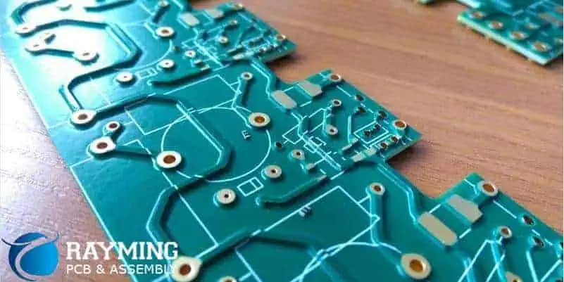
In the world of printed circuit board (PCB) design and manufacturing, copper thickness plays a crucial role in determining the performance, reliability, and overall functionality of electronic devices. This comprehensive article will explore the differences between standard copper thickness and high copper thickness, their applications, advantages, and challenges.
Understanding Copper Thickness in PCBs
Before delving into the comparison, it’s essential to understand what copper thickness means in the context of PCBs and how it’s measured.
What is Copper Thickness?
Copper thickness refers to the depth of the copper layer on a PCB. This copper layer serves as the conductive path for electrical signals and power distribution.
Measuring Copper Thickness
Copper thickness is typically measured in ounces (oz) or micrometers (µm). One ounce of copper spread over one square foot equals approximately 34.79 micrometers.
| Copper Weight (oz) | Thickness (µm) | Thickness (mils) |
| 0.5 oz | 17.5 µm | 0.7 mils |
| 1 oz | 35 µm | 1.4 mils |
| 2 oz | 70 µm | 2.8 mils |
| 3 oz | 105 µm | 4.2 mils |
| 4 oz | 140 µm | 5.6 mils |
Standard Copper Thickness
Standard copper thickness is the most commonly used option in PCB manufacturing.
Definition of Standard Copper Thickness
Generally, 1 oz (35 µm) copper is considered the standard thickness for most PCB applications.
Applications of Standard Copper Thickness
Standard copper thickness is suitable for a wide range of applications, including:
- Consumer electronics
- Computer peripherals
- Automotive electronics
- Telecommunications equipment
- Industrial control systems
Advantages of Standard Copper Thickness
- Cost-effective
- Widely available
- Suitable for most general-purpose applications
- Easier to etch and process
- Compatible with standard manufacturing processes
Limitations of Standard Copper Thickness
- Limited current-carrying capacity
- May not be sufficient for high-power applications
- Potential for overheating in high-current scenarios
- Less mechanical strength
High Copper Thickness
High copper thickness refers to copper layers that are thicker than the standard 1 oz.
Definition of High Copper Thickness
Typically, any copper thickness greater than 2 oz (70 µm) is considered high copper thickness.
Applications of High Copper Thickness
High copper thickness is often used in:
- Power supplies
- Motor controllers
- LED lighting systems
- Electric vehicle electronics
- Aerospace and military equipment
- High-frequency RF applications
Advantages of High Copper Thickness
- Increased current-carrying capacity
- Better heat dissipation
- Improved mechanical strength
- Enhanced signal integrity in high-frequency applications
- Reduced voltage drop in power distribution
Challenges of High Copper Thickness
- Higher material costs
- More difficult to etch and process
- Potential for overetching and underetching
- Increased overall PCB thickness
- Limited availability of compatible components
Detailed Comparison

Let’s break down the comparison between standard and high copper thickness across various factors.
1. Current-Carrying Capacity
| Copper Thickness | Current-Carrying Capacity |
| 1 oz (Standard) | Base reference |
| 2 oz | Approximately 2x of 1 oz |
| 3 oz | Approximately 3x of 1 oz |
| 4 oz | Approximately 4x of 1 oz |
High copper thickness allows for significantly higher current-carrying capacity, which is crucial for power electronics and high-current applications.
2. Thermal Management
Heat Dissipation Capability
| Copper Thickness | Relative Heat Dissipation |
| 1 oz (Standard) | Base reference |
| 2 oz | Approximately 1.5x of 1 oz |
| 3 oz | Approximately 2x of 1 oz |
| 4 oz | Approximately 2.5x of 1 oz |
High copper thickness provides better heat dissipation, reducing the risk of overheating and improving overall thermal management.
3. Signal Integrity
Impact on Signal Integrity at Different Frequencies
| Frequency Range | Standard Copper (1 oz) | High Copper (2 oz+) |
| Low (<1 MHz) | Good | Excellent |
| Medium (1-100 MHz) | Good | Very Good |
| High (>100 MHz) | Adequate | Good |
High copper thickness can improve signal integrity, especially at lower frequencies, due to reduced resistance and skin effect.
4. Manufacturing Considerations
Comparison of Manufacturing Aspects
| Aspect | Standard Copper (1 oz) | High Copper (2 oz+) |
| Etching Time | Shorter | Longer |
| Etching Precision | Higher | Lower |
| Drilling | Easier | More challenging |
| Plating | Standard process | May require special processes |
| Overall Cost | Lower | Higher |
High copper thickness presents more manufacturing challenges and typically increases production costs.
5. Mechanical Strength
High copper thickness provides better mechanical strength, which can be beneficial in applications subject to vibration or mechanical stress.
| Aspect | Standard Copper (1 oz) | High Copper (2 oz+) |
| Flex Resistance | Good | Excellent |
| Vibration Resistance | Adequate | Good |
| Pad Adhesion Strength | Good | Excellent |
6. Impedance Control
Copper thickness affects the impedance of PCB traces, which is crucial for high-speed and RF applications.
| Aspect | Standard Copper (1 oz) | High Copper (2 oz+) |
| Impedance Control | Easier | More challenging |
| Trace Width | Narrower for given impedance | Wider for given impedance |
| Suitable for High-Speed | Yes | Yes, with careful design |
Choosing Between Standard and High Copper Thickness
Selecting the appropriate copper thickness depends on various factors:
- Current Requirements: High-current applications generally benefit from thicker copper.
- Thermal Considerations: If heat dissipation is a concern, thicker copper may be advantageous.
- Signal Integrity Needs: High-frequency applications may require careful consideration of copper thickness.
- Mechanical Requirements: Applications subject to vibration or stress may benefit from thicker copper.
- Cost Constraints: Standard copper is more cost-effective for applications that don’t require high current-carrying capacity.
- Manufacturing Capabilities: Consider the manufacturer’s ability to work with high copper thickness.
Future Trends

As electronic devices continue to evolve, we can expect to see some interesting trends in copper thickness:
- Increased Demand for High Copper: With the growth of electric vehicles and high-power electronics, demand for high copper thickness PCBs is likely to increase.
- Advancements in Manufacturing: New techniques may emerge to address the challenges of working with high copper thickness.
- Hybrid Solutions: Combining standard and high copper thickness on the same board may become more common.
- Material Innovations: New copper alloys or alternative materials may be developed to enhance performance while managing costs.
- Miniaturization Challenges: As devices shrink, balancing the need for high copper thickness with size constraints will be an ongoing challenge.
Environmental and Sustainability Considerations
When comparing standard and high copper thickness, it’s important to consider the environmental impact:
Material Usage
| Aspect | Standard Copper (1 oz) | High Copper (2 oz+) |
| Copper Usage | Lower | Higher |
| Environmental Impact | Lower | Higher |
| Recyclability | Standard | Standard |
Energy Efficiency
While high copper thickness PCBs use more material, they can contribute to improved energy efficiency in the final product due to lower resistance and better heat dissipation.
Longevity and Reliability
PCBs with high copper thickness often have improved durability and reliability, potentially leading to longer product lifespans and reduced electronic waste.
Frequently Asked Questions (FAQ)
1. How does copper thickness affect the overall PCB thickness?
Copper thickness directly impacts the overall PCB thickness. Here’s a general guideline:
| Copper Thickness | Additional Thickness per Layer |
| 1 oz (standard) | Approximately 0.0014″ (35.56 µm) |
| 2 oz | Approximately 0.0028″ (71.12 µm) |
| 3 oz | Approximately 0.0042″ (106.68 µm) |
| 4 oz | Approximately 0.0056″ (142.24 µm) |
For a 4-layer board, switching from 1 oz to 2 oz copper would increase the overall board thickness by about 0.0056″ (142.24 µm). This can be significant in space-constrained designs or when working with specific enclosures. It’s important to consider this increase when selecting connectors, planning for assembly, and ensuring compatibility with other components in the system.
2. Can I mix different copper thicknesses on the same PCB?
Yes, it is possible to use different copper thicknesses on the same PCB, a technique known as “selective plating” or “zone plating.” This approach allows designers to optimize copper thickness for different areas of the board based on specific requirements.
Common scenarios for mixing copper thicknesses include:
- Using thicker copper for power planes and high-current traces
- Maintaining standard thickness for signal layers
- Employing thicker copper for heat dissipation in specific areas
While this technique offers design flexibility, it does come with some considerations:
- Increased manufacturing complexity and cost
- Potential challenges in maintaining consistent impedance across different areas
- Need for clear communication with the PCB manufacturer about requirements
When considering mixed copper thicknesses, it’s crucial to work closely with your PCB manufacturer to ensure feasibility and optimize the design for manufacturability.
3. How does copper thickness impact PCB cost?
Copper thickness can significantly impact PCB cost due to several factors:
| Factor | Impact on Cost |
| Raw Material | Higher copper thickness increases material cost |
| Processing Time | Thicker copper requires longer etching time, increasing production cost |
| Yield Rates | High copper thickness can lead to lower yield rates, affecting overall cost |
| Equipment Wear | Processing thick copper may increase equipment wear, indirectly affecting cost |
As a rough estimate, moving from 1 oz to 2 oz copper might increase the bare board cost by 10-20%, while going to 3 oz or 4 oz could increase costs by 30-50% or more. However, these are general figures, and actual costs can vary significantly based on the specific design, manufacturer, and order volume.
It’s important to balance the cost increase against the performance benefits. In some cases, the improved performance and reliability of high copper thickness can lead to overall system cost savings or improved product longevity, offsetting the higher initial PCB cost.
4. What are the key challenges in manufacturing high copper thickness PCBs?
Manufacturing high copper thickness PCBs presents several challenges:
- Etching Precision: Thicker copper is more difficult to etch accurately, potentially leading to issues with trace width consistency and spacing.
- Drilling: Thicker copper can cause more wear on drill bits and may require slower drilling speeds, increasing production time and cost.
- Plating: Achieving uniform plating thickness can be more challenging with high copper thickness, especially in high-aspect-ratio vias.
- Impedance Control: Maintaining precise impedance control is more difficult with thicker copper due to the increased impact on trace geometry.
- Registration: Aligning multiple layers accurately can be more challenging with thicker copper layers.
- Warpage: PCBs with unevenly distributed high copper thickness may be more prone to warpage during the manufacturing process.
To address these challenges, manufacturers may need to:
- Use specialized etching processes
- Employ more robust drilling equipment
- Implement advanced plating techniques
- Conduct more rigorous testing and quality control measures
These additional steps and requirements often contribute to the higher cost and longer lead times associated with high copper thickness PCBs.
5. How does copper thickness affect the choice of PCB laminate material?
Copper thickness can influence the selection of PCB laminate material in several ways:
- Thermal Expansion: Thicker copper has a different coefficient of thermal expansion compared to the laminate. This difference can lead to stress and potentially cause delamination or warpage. Laminates with better thermal stability (e.g., polyimide or high-Tg materials) may be preferred for high copper thickness designs.
- Adhesion Strength: Higher copper thickness requires laminate materials with stronger adhesion properties to prevent copper peeling, especially under thermal stress.
- Dielectric Constant: The effective dielectric constant of the PCB can be influenced by copper thickness, especially in high-frequency applications. This may require adjustments in laminate selection to maintain desired electrical properties.
- Flexibility: For flex or rigid-flex PCBs, the laminate needs to accommodate the stress introduced by thicker copper while maintaining flexibility.
- Heat Resistance: Laminates with higher heat resistance may be necessary to withstand the increased heat generated in high-current applications that often utilize thicker copper.
| Copper Thickness | Recommended Laminate Considerations |
| Standard (1 oz) | Standard FR-4 usually sufficient |
| 2 oz | High-Tg FR-4 or enhanced materials |
| 3 oz and above | High-performance laminates (e.g., polyimide, ceramic-filled PTFE) |
When working with high copper thickness, it’s crucial to consult with both the laminate supplier and PCB manufacturer to ensure compatibility and optimal performance of the final product.
In conclusion, the choice between standard and high copper thickness in PCB design is a critical decision that impacts various aspects of performance, manufacturability, and cost. While standard copper thickness remains suitable for many applications, the growing demand for high-power and high-performance electronics is driving increased adoption of high copper thickness PCBs. By carefully considering the specific requirements of each application and weighing the trade-offs, designers can make informed decisions to optimize their PCB designs for both performance and cost-effectiveness.