Embedded Electronics Design: Making a Big Splash with Tiny Technology

Embedded PCB

Are you ready to enter the wondrous world of embedded electronics creation? Despite the complexity of the field, with suitable instruments and a little bit of knowledge, it is possible to create incredible products that bring your designs to life. Embedded electronics design facilitates the production of numerous products, including smart cards, satellites, and communication systems. This article will discuss the stages of designing embedded electronics, the tools used, the applications and benefits, and the market’s future. So prepare to explore the intriguing world of embedded electronics design!

Embedded electronics design

Embedded electronic design develops and designs electronic systems embedded in various products. Additionally, these systems are tiny, low-powered, and have limited computing capabilities. Their design enables them to carry out certain activities or duties. Embedded systems are helpful in various areas, such as medical devices, consumer electronics, industrial control systems, and automotive systems.

Types of Embedded Electronics Design

embedded iot
  • Standalone Embedded Electronics Design:

Creating a standalone gadget that performs a specific function is the goal of standalone embedded electronics design. These systems can function autonomously without access to other systems or devices.

  • Internet of Things embedded electronics devices:

To engage in the Internet of Things, electronic devices with embedded circuitry must be able to connect to the internet and communicate with other devices and services. IoT-embedded electronics include smart homes, wearable electronics, and industrial tracking systems.

  • Electronics architecture for embedded networks:

The goal of network-integrated electronic design is to create gadgets that can communicate with other networked gadgets. These systems must be able to communicate with other devices in real-time to link to external networks or devices.

  • Mobile embedded electronics design:

Designing moveable, environment-adaptable devices is the goal of the area of embedded electronics known as “mobile embedded electronics design.” These technologies include portable measurement instruments, handheld medical devices, and mobile payment terminals. Additionally, these systems are frequently wirelessly linked, lightweight, portable, and energy efficient.

YouTube video

Software Tools Used in Embedded Electronics Design.

The following are some of the tools that perform the embedded electronics design procedure:

1. ARM Keil

The ARM Keil toolkit is suitable especially for designing embedded electronics. Programmers can create code for various ARM-based microcontrollers and microprocessors using this set of tools. It comes with tools like an assembler, translator, linker, debugger, and others that aid in developing software for ARM-based microcontrollers. Drivers, libraries, and product support are also part of the package. It is simple to use and offers a variety of features to aid developers in producing stable embedded apps.

2. Arduino:

Arduino is an open-source platform called used to create embedded electronics apps. It offers a straightforward and effective programming language for creating microcontroller-based applications. Furthermore, Arduino is built on the C++ programming language; however, it can operate with Arduino boards due to its design. It offers a broad selection of software and hardware support for various microcontrollers. It is also an excellent option for prototyping and creating a wide range of embedded electronics projects because it is compatible with multiple hardware and software platforms.

3. MATLAB:

MATLAB is an integrated development environment (IDE) for software creation and numerical computing. The design of embedded electronics provides a wide variety of application-specific tools. Thanks to its user-friendly interface, developers can rapidly write, test, and simulate code. It is also beneficial for data processing and visualization. Various toolboxes are also available, which help create embedded electronic designs.

4. NetBeans:

NetBeans is a programming platform that can make applications for embedded electronics. An editor, debugger, and compiler are the programming tools it offers. It is an excellent option for embedded electronics applications because it is also interoperable with various microcontroller and processor architectures. In addition, the extensive collection of the APIs provided by NetBeans also allows for the development of user interfaces and external hardware communication.

5. Eclipse:

Eclipse is a free, expandable IDE for designing embedded devices. It comprises a code editor, debugger, and compiler, among other many tools and functions it offers. It also provides a variety of plugins that facilitate the creation of embedded apps. In addition, it is compatible with various processor and microcontroller architectures, making it suitable for embedded electronics applications.

6. Use Visual Studio

Visual Studio is a development environment for building embedded electronic designs. A code editor, debugger, and compiler are some of the many functions it offers. It also provides libraries and APIs for building user interfaces and interacting with third-party devices. It also works with various microcontroller and processor architectures, making it an excellent option for embedded electronics applications.

7. MPLAB X

The MPLAB X toolkit was mainly for the creation of embedded electronics applications. A code editor, debugger, and compiler are some of the many functions it offers. In addition, it works well with various microcontroller and CPU designs, making it the best option for embedded electronics projects. Additionally, it provides APIs and libraries for building user interfaces and interacting with third-party devices.

8. Qt Creator:

Qt Creator is an open-source IDE for developing applications for embedded devices. A code editor, debugger, and compiler are just a few of the many tools offered by Qt Creator. It is a fantastic option for embedded electronics applications because it is compatible with various microcontrollers and processor architectures.

The design process for embedded electronics design.

FULL PCB MANUFACTURING Quote

The following steps can help in designing embedded electronics:

ยท Analysis of Requirements:

Analyzing the project’s needs is the first phase in the design process. This step includes recognizing the issue you need to fix, comprehending the project’s goals and objectives, and figuring up the functional specifications for the system. Also, when analyzing the requirements, please consider the technological, financial, and legal limitations that could affect the design.
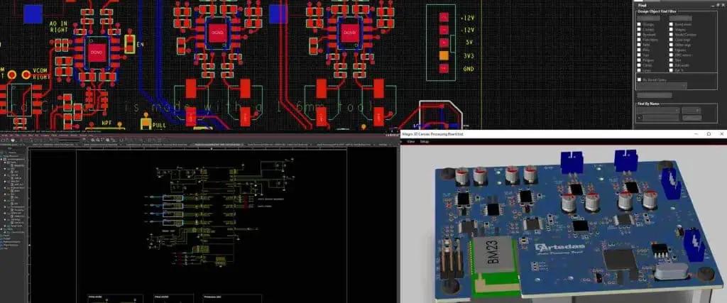
ยท Schematic Design:

 Following the definition of the requirements, you must create the system’s schematic diagram. To do this, please choose the proper components, and organize their connections. The PCB design appears according to the schematic, a pictorial representation of the electronic circuit. Also, remember to assess any applicable safety or regulatory standards in the schematic design.
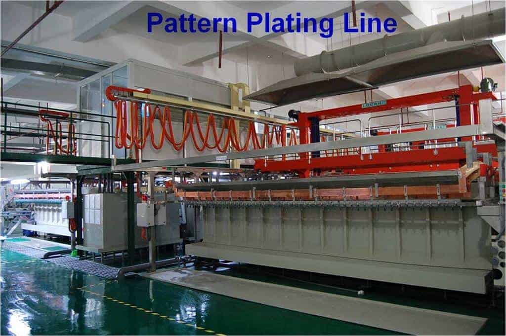
ยท PCB Design:

Having completed the schematic design, now create the printed circuit board (PCB). Making a layout of the board’s components and connections is necessary for this. You must tailor the design to the system’s dimensions, form, and functioning. A PCB design software will help you produce manufacturing files and construct the layout for the PCB fabrication process.

ยท Development of the prototype:

We now construct the system prototype after the PCB design. This step entails assembling the parts on the PCB and ensuring the system works. In addition, the prototype helps in the testing ground to gauge the system’s effectiveness and spot any unresolved design problems.

ยท Firmware development:

After evaluating and validating the prototype, you now develop the system firmware. The software regulates how the hardware parts act. Usually, a low-level programming language like C or Assembly is applicable in writing it. Writing, testing, debugging the code, and integrating it with the hardware components are all steps in the firmware development process.

ยท Testing and approval:

Finally, we must perform testing and verification to complete the design process. This step entails tests to ensure the system satisfies the functional requirements and functions dependably under various circumstances. For example, the acceptance testing may include several performance, safety, and regulatory tests to ensure the system complies with all applicable standards and requirements.

Application of Embedded electronics design

embedded-components-in-pcb

ยท Smart cards:

Embedded electronics design is helpful in the creation of smart cards. Access control, payment systems, identity, and transportation are just a few of the uses for smart cards, which are plastic cards with an integrated chip. Smart cards consist of a microprocessor, memory, and communication interfaces. The memory stores data and programs while the microcontroller runs the card’s applications. Additionally, the communication interface enables the smart card to communicate with other devices, such as card readers.

ยท Satellites:

Embedded electronics design is essential for the creation of satellite systems, which help in areas such as communication, weather monitoring, and remote sensing. To design satellite systems, designers must integrate various elements, including antennas, power systems, sensors, and communication interfaces. Additionally, they should consider the weight, size, and power consumption in the embedded electronics design of a satellite system.

ยท Telecommunication:

Embedded electronics design help in communication across large distances. Telecommunication system uses various elements such as antennas, transmitters, receivers, and communication interfaces. Designers must integrate these elements into telecommunication system designs and create and control software for the interface.

ยท Digital consumer electronics:

Designers develop digital consumer electronics, including smartphones, tablets, and laptops, using embedded electronics design extensively. Additionally, embedded systems control the functionality of these devices, including the display, audio, and touch interfaces. In addition, the designers should also create software to operate and communicate with these components.

ยท Missiles:

The development of missile systems, helpful for both military and defense purposes, uses embedded electronics design. Therefore, designers must integrate numerous parts, including propulsion systems, guidance systems, sensors, and communication interfaces, while designing a missile system. Furthermore, they should consider weight, size, and power consumption when designing embedded electronics for missile systems.

ยท Central heating system:

The development of central heating systems, which help heat houses and buildings, uses embedded electronics design. The primary heating systems consist of various parts, including thermostats, sensors, valves, and communication interfaces. The embedded electronics design of central heating systems must include energy efficiency and user-friendliness.

ยท GPS systems:

GPS (Global Positioning System) systems help in navigation and location-based services. Embedded electronics design allows for the construction of these GPS systems. GPS systems include antennas, receivers, processors, and communication interfaces. Designers and manufacturers should consider the accuracy, dependability, and power consumption in the embedded electronics design of GPS systems.

ยท Fitness trackers:

The creation of fitness trackers, which help monitor physical activity and fitness objectives, uses embedded electronics design. Fitness trackers use sensors, CPUs, memory, and communication interfaces. Designers should consider reliability, power consumption, and accuracy when designing fitness trackers.

ยท Medical devices:

Embedded electronics design in medical sectors helps design equipment such as pacemakers, insulin pumps, and monitoring systems. Medical devices consist of sensors, CPUs, memory, and communication interfaces. In their creation, designers should consider the device’s power consumption, dependability, and safety.

Benefits of Embedded Electronics Design

Below are some of the critical benefits of embedded electronics design:

ยท Improved Functionality:

Embedded electronics design enables them to perform specific functions, and designers can tailor them to meet the exact requirements of a particular application. In addition, by integrating specialized hardware and software, embedded systems can offer enhanced functionality, increased reliability, and improved performance.

ยท Reduced Cost:

Embedded electronics design helps reduce costs by streamlining the design process, reducing the number of components required, and eliminating the need for external components. As a result, manufacturers can reduce production costs, increase efficiency, and improve product quality by designing a single integrated system.

ยท Increased Efficiency:

Embedded systems have a design that enables them to perform specific functions efficiently, often with a small form factor and low power consumption. This makes them ideal for applications where space, power, and performance are critical factors, such as mobile devices, wearables, and automotive systems.

ยท Improved User Experience:

Embedded electronics can enhance the user experience by providing intuitive interfaces, efficient operation, and reliable performance. For example, a smart home system can offer convenient control over household devices, while a wearable fitness tracker can provide real-time feedback on fitness goals.

ยท Enhanced Safety and Security:

Embedded electronics help improve safety and security by providing real-time monitoring, control, and response capabilities. For example, a home security system can alert homeowners to potential threats, while an automotive system can detect and respond to potential hazards on the road.

ยท Customizability:

Designers can customize embedded systems to meet the specific requirements of a particular application. This customization allows manufacturers to tailor the design to the needs of their customers, resulting in a more optimized, efficient, and effective product.

ยท Scalability:

Manufacturers can design embedded electronics to scale from small to large-scale applications, making them suitable for a wide range of products and systems. Scaling allows manufacturers to expand their product offerings and reach new markets.

The future of Embedded electronics design Market

โ€ข New Technology Will Aid in the Development of Embedded Electronics:

Embedded circuitry design will probably spread across more industries as technology advances. For instance, designers believe that the Internet of Things (IoT) and the growing demand for automation in the manufacturing sector will drive the growth of embedded systems. The advancement of embedded electronics design will also be greatly impacted by new technologies like 5G, AI, and ML.

โ€ข Embedded systems are cost-effective due to a variety of programming techniques:

New programming languages, frameworks, and tools have significantly reduced the cost of developing and building embedded electronics. This programming method allows engineers to work more efficiently and successfully, which reduces the time and cost required to create a product. Additionally, it has become simpler for startups and small businesses to join the embedded electronics industry as open-source hardware and software have grown in popularity.

โ€ข Growing Demand for Cybersecurity:

The need for cybersecurity will rise as the number of embedded devices rises. Critical infrastructure areas like transportation, healthcare, and electricity frequently use embedded systems. Cyberattacks against these networks could be disastrous and are possible. Designers foresee the development of secure embedded electronic designs, and that there will be a high demand for companies that can provide security solutions.

โ€ข Growing Demand for Wireless Connectivity:

There has been a noticeable increase in demand for wireless connectivity as a consequence of the growth of the Internet of Things (IoT) and the popularity of mobile devices. In light of this, there will undoubtedly be a sizable market for embedded electronics with Wi-Fi, Bluetooth, and 5G wireless networking capabilities. Because of this, system makers will also need to develop systems that are inexpensive, power-efficient, and compatible with a variety of devices.

โ€ข Stress on sustainability:

Designers place a strong emphasis on sustainability in product design in light of the growing worry over climate change. This tendency is most likely to continue in the field of embedded electronics. The designers predict that as a result, there will be a greater demand for creating products that are energy-efficient and use sustainable and ecologically friendly materials. In order to reduce the environmental effect of their work, product designers will need to consider every phase of the creation process, from conception to disposal.

Challenges Faced in Embedded Electronic Design

While designing embedded electronic designs, the following are the challenges youโ€™re likely to encounter:

ยท Small Form Factor:

The biggest challenge with small form factors for embedded electronics design is that it needs greater accuracy to accommodate all required components. To fit into the smallest feasible area, the product must nevertheless provide room for the placement of its components. Since the components require a small area, achieving and guaranteeing maximum performance is challenging. In addition, the design must be flexible enough to allow for any necessary alterations in the future. Finally, designers should design it lightweight and sturdy since the compact form factor often necessitates a smaller and lighter design than typical.

ยท Low Energy:

In the design of embedded electronics, a low energy footprint is crucial. The power consumption must be as low as possible to guarantee top performance and lower the product’s price. Concerning items used in battery-powered applications, this is particularly crucial. This feature is significant for products that help in battery-powered applications. To achieve this, the designer must optimize the design to reduce power consumption. This process may involve using energy-efficient components and optimizing the power supply. Additionally, the design must be able to run at low voltages since it helps reduce power consumption.

ยท Long-term Stable Performance Without Upkeep:

The design must deliver stable performance without any upkeep or replacements. This aspect is beneficial for items applicable in commercial or medical settings. The design must be durable and resist wear and tear over time to benefit medical and commercial setups. The design must also be able to identify any possible issues before they arise to prevent unplanned downtime,

ยท Insufficient Flexibility for Running Apps Across Embedded Systems:

Designing embedded electronics can be challenging when running applications over embedded systems requires more flexibility. This flexibility is necessary because the design must be able to handle growing amounts of data as well as the simultaneous use of multiple applications. A growing amount of data requires a design that can accommodate several operating systems and has adequate memory to manage the data. In addition, the design must be flexible enough to accommodate upgrades as needed and handle the most recent software and technology.

ยท High Power Dissipation of Embedded Electronics:

The high-power dissipation of embedded electronics can be a challenge for embedded electronics design. This aspect is because the design must dissipate heat generation from the components without any damage. Therefore, manufacturers must design the product to ensure optimal airflow and dissipate the heat to the environment. Additionally, the design must accommodate any other cooling systems that may be needed, such as fans or heatsinks.

ยท Issues with Testing Embedded Electronics Designs: 

Given the complexity of the design, testing embedded electronics designs can be complicated. It must undergo extensive testing to ensure the design performs well in the field. For example, the designer may need to test several configurations, components, and temperatures. Additionally, they should test the design in various contexts to ensure that it can handle multiple circumstances. In addition, they should evaluate any possible issues like EMI or electrical noise in the design.

ยท Insufficient Functional Safety:

An essential part of assuring a product’s safety is the functional safety of an embedded electronics design. The product’s design must take all necessary precautions to guard against any possible damage or injuries. Manufacturers must use redundant components and robust design strategies to avoid potential errors. Moreover, it is also necessary to examine the design for any possible safety flaws, such as improper wiring or connections.

ยท Increased cost and time-to-market:

While developing embedded electronics, it’s crucial to consider the long time to market and higher costs. The design must satisfy the customer’s requirements in a timely and cost-effective manner. Using less expensive components or more economical production techniques may help achieve a convenient and cost-effective design. Designers should ensure that testing and production are easy to ensure that they deliver the product on time. Additionally, they should also ensure that the product is flexible to update and modify quickly so that they can keep up with the market’s constant change.

Conclusion

Embedded electronics design is an incredible field to explore. With the right knowledge and tools, you design amazing products to help people in many aspects. Embedded electronics design has various applications and benefits such as smart cards, satellites and weapons. Get ready to dive into the wondrous world of embedded electronics design!

Your Guide to Understanding How Plating PCB Improves a Circuit Boardโ€™s Aesthetics

pcb edge plating

You must have seen someone plating a hair and you wondered why it is important to do so. While one of the major reasons is to change the appearance, one core reason is to help the hair grow faster and have a good texture. A similar perspective can be used to describe the plating of PCBs.

This sometimes appears to be a confusing concept, considering that it is often intertwined to mean surface finishing. And while the two can coexist, they do have a couple of differences. In this article, we explain in-depth, what PCB plating means.

What Does It Mean when a PCB is Plated?

A Printed Circuit Board (PCB) is plated for different reasons, but one of the most outstanding is that the process helps to facilitate the flow of current within and around the board. As you know, a circuit board thrives on current and the distribution of the same to the components in the electronics.

The Plating Process Simplified

To simplify how the process works, we will go this way: it is an electromechanical process. The process involves the deposition or insertion of a metal (usually copper) to the PCBโ€™s surface areas. A similar deposit is made into the plated through-holes or the holes drilled on the board.

When is PCB Plating Required?

PCB pattern plating line

In recent years and with the advancement of the modern circuit board processing technologies, plating of PCBs has become a trend when working with multilayer circuit boards. The goal is to facilitate the interconnection of the different layers and components that go into the making of such PCBs.

The Two-Way PCB Plating Process

This is where there is a bit of confusion and you need to pay an attention to how it works. Commonly, circuit boards are plated through the via process, where copper is used.

For the via plating, the Plated Through Hole (PTH) process commonly called vias is used. The process entails using a metal (copper) to fill the drilled holes on the board as a way of channeling the current to move from the boardโ€™s surface to the inner layer. The currentโ€™s pathway can also be made in a way that it moves from one surface to the other or between two internal layers on the PCB.

Surface finishing is the name of the other plating process for PCBs. It is usually regarded as the second step of the process and rightly so because of the designation for covering the surface copper traces. Doing so helps to protect those traces from overt exposure to adverse environmental risks, such as contamination, oxidation and moisture.

The Processes for PCB Plating

To start plating your PCB, it has to begin with an electroless process where the metal (copper) is to be used. Before we continue, let us highlight a couple of reasons why copper is the most preferred for this via plating process:

  • Robust Connection: due to the reliability of the material and the internal properties, it is better to use copper for via plating, as it provides a robust connection. Such connection is needed to facilitate the flow of current from one layer to the other, as well as from one PCB surface to the next.
  • Pad and Conductor Thickness: the use of copper helps to increase the copper thickness of the conductors and the pads.

With that being noted, let us now go deeper into the copper plating process for PCBs, which is an electroless process.

1. Chemical Coating

A chemical coating process is used to place or deposit a thin copper layer to the PCBโ€™s surface. A similar process is used to make a similar deposit in the interior of the drilled holes in the circuit board.

The goal of the chemical coating process is to create a thin metal base both in the drilled holes and on the circuit boardโ€™s surface. That, in turn, lays the foundation for the electroplating process to commence in earnest.

2. Board Preparation

You will now prep the circuit board for the electroplating process by implementing a couple of strategies, such as:

  • Hole Cleaning: the drilled holes are to be cleaned, as there is a possibility of having getting filled in some places by the contaminants and residues generated while the drilling process was on.
  • Micro Etching: the interior of the drilled holes is now to be subjected to micro etching. As the name signifies, it is a minimal etching process โ€“ and one that aims at improve the copper binding possibilities.

3. Photoresist Material Application

The electroplating process begins. The step here is to add the photoresist material to both the bottom and top of the PCB. Once these parts are covered with the material, the photoresist material is to be exposed to Ultraviolet (UV) light.

While doing this, make sure that the exposed parts are limited to the areas on the PCB that donโ€™t have patterns. That is, those areas or surfaces where the plating of the metal circuitry patterns are to be done.

4. Wash off the Photoresist

The photoresist material can now be washed off the PCBโ€™s surface (i.e., top and bottom). Note that it is only the pliable photoresist material that gets washed off. That is, the part that covers the circuitry patterns.

Once this is done, what would be left is the remaining parts of the circuit board that are masked or well-covered by the hardened photoresist material.

5. Copper-to-External Layer Plating

It is now the time to make an electroplating of the most parts of the copper to the external layers, as well as into the drilled holes. The processes to achieving this include:

  • The circuit board would be connected to a negative charge, also called the cathode. The charge has to be that of an electrical current.
  • Step 2 is to immerse or dip the copper into a chemical bath for plating.
  • The third step will see to the drawing of the dissolved copper through the solution to the negative charge. It would then be deposited onto the exposed copper circuitry.
  • An even or uniform copper layer has to be produced and that can be done via the dipping of the circuit board into the plating and cleaning solutions/baths. This has to be done under strict, controlled conditions to get the best results.
  • It is now the time to plate the tin onto the copper. This is a measure implemented to bolster the circuitryโ€™s protection.
  • The next step is to remove both the photoresist (material) and the non-circuitry copper. The process used here is etching.
  • The removal of the tin that was previously plated to the copper is the last step. When this is done, you will be left with the bare copper circuitry.

Comparing the Electroplating and the Electroless Plating Processes

FULL PCB MANUFACTURING Quote

From the above discussions, you could see an interchange between the electroplating and the electroless plating methods for plating circuit boards. They are quite different and we want to quickly point out some of the differences.

Electroplating PCB Plating Method

This refers to the PCB copper plating method that doesnโ€™t rely on the use of external electric power. Rather, it uses a chemical reaction, which, in turn, facilitates the reduction of metal atom.

It is important to mention that the particles or metal ions in the reducing agent solution getting in contact with the catalytic metal leads to the transformation to a metal solid. This, in turn, triggers the required reaction that brings forth the required atom reduction of the metal (copper).

Electroless Plating

When a PCB is subjected to electroless plating, it means that it doesnโ€™t use either plating baths or an external power.

The attributes include usability with different materials, such as copper, gold plating and silver. You can also take advantage of the electroless PCB plating method to derive improved solderability, reflectivity, and changing conductivity. It is also reliable for the availability in different sizes, and the support for different materials.

Despite being an affordable variant to the electroplating method, the electroless method has a couple of downsides, such as:

  • Regulation difficulties
  • It is slower process than the faster electroplating method.
  • It is almost impossible to derive or produce thick plates using the electroless plating method.

The Major PCB Plating Methods You Need to Know

There are four (4) major methods or ways you can plate a Printed Circuit Board (PCB). These methods include the popular PCB Through Hole plating process, down to the brush plating, reel linkage plating and finger-plated plating.

Each of these methods offer distinct processes and following these to the latter assures of the best results.

With that being said, let us now extensively talk about the different methods available for you to pick from.

1. Finger-Plated PCB Plating

Another name for this is protruding partial plating. It includes the use of three (3) major items to achieve excellent circuit board plating. These are the items and how they all make a difference:

  • Rare Metals: these metals are to be plated on any of the following places on the PCB: edge joints of the PCB, the boardโ€™s edge connectors and at the gold fingers. The primary goal of the plated rare metals is to reduce the circuit boardโ€™s contact resistance. It also helps to bolster or increase the PCBโ€™s abrasive resistance.
  • Gold Finger: this uses either the manual or automatic plated technology to bolster the plating.
  • Gold: this is another item and it is often plated on the inner nickel coating of the circuit board edges connectorโ€™s protruding contact head.

2. Brush Plating

This is also one of the popular plating methods for PCBs. As the name suggests, it has to do with brushing โ€“ but it goes deeper than that. Here are some of the things you need to know about brush plating for PCBs:

  • Part-Plating: not all the parts of the circuit board are to be immersed or dipped into the electrolyte. Only a limited area is dipped into the same during the PCB plating process.
  • Plating Process: for the best results and to prevent an overall plating, a chemically-reactive anode, such as graphite has to be wrapped in a cotton stick or any other absorbent material. It is then used to bring the electrolyte (solution) to where the plating is most required on the PCB.

3. The Plated Through Hole PCB Plating Method

This is the most used process for plating circuit boards, especially the multilayer PCBs. It is prioritized due to the extensive features it offers. Sometimes, it is compared to the non-plated through hole process.

First, let us understand what the Through Hole Technology or THT is all about. According to Wikipedia, this has to do with โ€œthe manufacturing scheme in which the leads on components are inserted through holes drilled in Printed Circuit Boards (PCBs).โ€

Thus, the process leverages on the already-drilled or existing holes in the PCB to integrate the leads on the circuit board components.

Also, the Through Hole Technology (THT) thrives on the soldering of these holes to the pads on the opposite side. The soldering process can either be by the use of automated pick-and-placed machines or manually done, by hand.

Here are some quick facts about the plated through hole process:

  • It uses the electroless copper plating method.
  • Coverage: the Plated Through Hole (PTH) plated method is considered to be through hole, only if it is able to go through the entire PCB. This is important because this plating method is done to enhance the flow of current throughout the circuit board.

The following attributes define the process of using PTH for your circuit board:

  • Compact PCB Size: it is possible to achieve a smaller footprint for your circuit board, using the Plated Through Hole (PTH) method. It is attained due to the vertical-stacking of the circuit board via the integration of the Plated Through Hole (PTH).
  • Current Flow: the plated through hole process is designed to facilitate an all-around flow of current within the PCB. It is expected that current would flow to the following places: to the other side of the PCB, through the circuit boardโ€™s non-conductive substrate, and through the components on the PCBโ€™s side.

Plated Through Hole (PTH) Vs. Non-Plated Through Hole (NPTH)

wrap plating
wrap plating

If a circuit board can be plated, what is also the possibility of not having it plated? This brings us to the discussion on some notable differences between the Plated Through Hole (PTH) and the Non-Plated Through Hole (NPTH) plating methods for PCBs.

First, understand that a circuit is subjected to the through-hole plating method because of the need to facilitate current flow to different parts of the board. It is also a measure aimed at plating a thin copper layer onto the walls or holes drilled in the PCB. In addition to boosting the electrical connectivity of the surfaces, it is also a means to improving the mechanical stability and lowering the resistance between the copper tracks and componentsโ€™ leads.

On the other hand, the non-plated through hole plating method doesnโ€™t have the most important ingredient that the PTH has โ€“ copper plating. To this end, it doesnโ€™t provide or support the electrical properties that the PTH supports.

These are some of the additional differences between the PTH and NPTH plating methods for PCBs:

  • With the PTH method, copper is plated onto the walls of the holes drilled on the PCB, while the same is not obtainable with the NPTH method.
  • The electroless plating process enhances the conductive properties of the inner walls of the holes. For the non-plated through hole plating, no electrical or conductivity properties are obtained, due to the absence of copper plated onto the holesโ€™ walls. This, in turn, prevents the barrel of the hole from holding any electrical function.

4. Reel Linkage Selective Plating

This can be a manual or automated plating process and which is based on the reel-to-reel plating method. It is to be noted that the following attributes make the plating process unique:

  • Selective Deposition: it supports the selective or handpicked deposition of metals, such as contact pins and pins. These are to be deposited on the following: connectors, flexible PCBs, transistors and Integrated Circuits (ICs).
  • Plating Process: both the manual and automated process can be used. However, for the best results and to facilitate bulk plating, it is best to go for the automated process called batch welding.
  • Plating Procedure: using reel linkage selective plating on PCBs involves the coating of a portion of the metal copper coil plate. The coating must be done with a resist film. Note also that the plating procedure must only be performed on the selected portion of the copper foil.

The Processes for Surface Plating of PCBs

This is the second procedure involved in the plating of Printed Circuit Boards (PCBs). It has to do with the โ€œsurface preparationโ€ of the PCB to have a defined outlook. For this purpose, a wide range of methods are used.

The definition of surface plating can be looked at from different perspectives:

1. Suitable Surface

One of the reasons for finishing or smoothening the surface of PCBs is to make it readied for the solderable components to be able to pass through. This comes in handy during the Printed Circuit Board Assembly (PCBA) process.

2. Environmental Protection

Also called surface finishing, the surface plating method for PCB refers to the processes taken to protect the boardโ€™s surface from overt exposure to the harsh environments. This is important due to the fact that the drilled holes and pads are to be left open after the initial plating process. Leaving these open exposes them to potential hazards, such as deterioration and oxidation of the copper.

To this end, making a surface finishing is a measure aimed at covering/plating the exposed copper for the protection from the aforementioned hazards.

Surface Finishing Options for PCBs

Now, your Printed Circuit Board (PCB)โ€™s surface can be finished or plated with any of the following methods:

1. Electroless Nickel Immersion Gold (ENIG)

Also called immersion gold plating, ENIG refers to the two-layered metal coating, whereby one of the layers of nickels is chemically-plated to the circuit board. The other layer of nickel serves as a source of protection for the exposed copper. It is also protected from oxidation by using a thin layer of gold.

As an electroless PCB plating method, ENIG plating doesnโ€™t require electric. It may also align with immersion to create a formidable metallic barrier.

2. Hot Air Solder Leveling

Also known as HASL, it refers to the circuit board surface finishing method that requires the dipping or immersing of the circuit board into hot solder. An air knife will be used to level-off the excess solder after the plating.

Despite being an affordable surface finishing process for PCBs, the HASL method tends to leave behind lots of uneven surfaces, despite the passage through hot blasts of air for leveling. To this end, there might be solder bridging issues arising from this.

3. Immersion Tin

Also called immersion tin plating, it has to do with the plating process that requires the use of tin. Some of the advantages of using immersion tin plating for your PCB surface finishing process include:

  • No lead is required.
  • The absence of lead and the associated process also means that the process is RoHS-compliant.

On the flipside, you may not want to go ahead with the immersion tin plating due to the creation or leaving behind of tin whiskers. This, in turn, creates connections issues between the components.

Wrapping Up: Why Plating is Important in the PCB Production Process

As Printed Circuit Boards (PCBs) form a bond between the components and the overall functionalities of the electronics; it makes sense to have them designed the right way.

The benefits of plating a PCB include but are not limited to providing a clean platform for soldering to take place. You also want to plate the circuit board, because of the aesthetic appeal it brings, the uniformity of the surfaces, and the protection of the components from contamination, moisture and oxidation.

At Hillman Curtis, we help recommend the best plating method to choose from (between PTH and NPTH). We also help you choose the best surface finish for your PCB.

What are the Benefits of AOI PCBA?

AOI PCBA

Automated optical inspection, a crucial procedure used in Circuit board fabrication and Circuit board assembly in addition to PCB tests, is crucial for PCB fabrication.

To ensure that the product does have a high quality before it leaves its production line or that your PCB is free of any manufacturing flaws, it performs an efficient and precise function in identifying the electronics assemblies as well as your PCBs.

What Does Automated Optical Inspection Mean?

AOI can be described as a machine-based technique employed to inspect and examine printed circuit boards (PCBs) for possible flaws such surface flaws, dimensional flaws, and component placement flaws. It is challenging and impractical to manually verify the circuit boards as they get more complex, hence AOI has a significant function in checking these PCBs after assembly.

Also, it has a significant impact on achieving the required product quality along the manufacturing line at a reasonable price.

The Benefits of AOI PCBA

FULL PCB MANUFACTURING Quote

Positional accuracy

Positional precision in production and inspection tools is becoming more crucial as component sizes shrink. The AOI PCBA system must have the sub-pixel accuracy for its rule-of-thumb, that ensures the availability for that system to locate little deviations in positions which can lead to the 01005 defects and problem.

Reduced Cost

With PCBA AOI test, the PCBโ€™s pass rate can be improved which will end up reducing the cost as well.

Multiple inspection targets

The AOI test is effective for circuit board assembly as well as PCBs. In terms of PCB, it examines for flaws including shorts, openings, and inadequate solder. But, it inspects several things for PCB assembly, like component soldering, values, and polarity.

Programmable lighting

For all machine vision applications to get the appropriate results, illumination is crucial. It is hard to discover a single light source which can identify all fault circumstances given the dynamic nature of electronics production. To ensure that the component as well as PCB layouts have the broadest fault coverage, the dynamic light becomes crucial. PCBA AOI test may set up light arrays which are extremely adjustable inside its inspection software due to the cost decrease of the light-emitting diodes.

Also, the AOI test may dynamically raise the image’s contrast, making it simple to spot a variety of fault circumstances in diverse colors from various perspectives.  Lighting programming lighting is a crucial technique for ensuring the greatest detection range.

Network-capable softwares

Data gathering and retrieval is a crucial component of any AOI PCBA system. The information can take the shape of a written output, an image collection, a database, or a medley of other formats. The majority of AOI PCBA systems have a fundamental purpose of gathering data, but retrieving that data is frequently more difficult and is dependent on how the production line is set up.

Excellent Flexibility 

Also, AOI PCBA is useful for all the stages in the process of fabrication with respect to the cost and needs tolerance capacity.

In addition, since most errors are the consequence of soldering process failure, doing an AOI test following reflow soldering can decrease associated costs and improve inspection effectiveness. Also, it may change the manufacturing or assembly settings right away to make the following goods appropriately.

Reasons why AOI PCBA is Very Important

SMT AOI
SMT AOI

Your product would function if the circuit board design is accurate and you put the right parts together in the proper order. It will concentrate on identifying and fixing any fabrication or manufacturing faults throughout production.

Without a doubt, AOI is a crucial inspection method to verify and evaluate the caliber of the PCB manufacturing and to address any issues or flaws at any time during process flow. The fact that AOI represents the printed circuit board’s quality gate ensures that designers can provide a high-quality board to you.

Your Circuit board is the brain of any device in many aspects, making it an essential part with strict design requirements. Also, as printed circuit boards grow smaller, they will become more complex. Even while a board may appear to be relatively basic, it may have thousands of different soldered joints, that implies a manual examination might or might not be feasible.

So, the easier and more affordable it is to prevent duplicating the same issue on a bigger scale, you must locate the flaws earlier during the process of manufacturing. In other words, if you’re involved with the PCB manufacturing industry, AOI is essential.

What types of flaws are detectable during AOI PCBA?

Surface flaws (including nodules and scratches), dimension flaws (including open circuits, thinner solder, and short circuits), incorrect components, lost components, and improperly arranged components may all be detected by AOI.

Component offset, the polarity of the component, component absence or presence, component skew, flipped component, area defects, insufficient paste all around leads, absence of population tests, lifted leads, paste registration, as well as components that are severely damaged are some of the issues that can occur with a PCBA having components.

Short circuits, violations of line width, spacing violations, surplus copper, missing pads, cuts, improper component mounting, and hole breakage for PCB boards (whether the via will be going out of its pads).

Better PCB assemblies are produced thanks to the automated inspections

A PCB may include several hundred separate nets connecting hundreds of different components having thousands pins.

Visual inspection is incapable of accurately examining each of the hundreds of locations on every produced pcb board assembly. Many of the most attentive rework experts become tired of inspecting and find it impossible to pay attention to everything at once, like searching for something like a needle inside a haystack.

On the contrary, employing AOI systems inside the manufacture of circuit boards will identify assembly or fabrication faults and inform the operators of their results. With this knowledge, the rework professionals can concentrate on fixing any issues. In comparison to what is feasible with conventional inspection procedures, AOI PCBA systems have developed a more dependable inspection process.

3D PCBA AOI Inspection Benefits

Among the methods used to gauge the PCBA assembly’s businesses is AOI PCBA testing Circuit board capabilities. Nowadays, the majority of assembly businesses in the sector employ 2D Circuit board AOI technology, but this low-level equipment does have certain disadvantages in testing, including a lack of knowledge on printing soldering and glue, as well as mistakes frequently happening during testing.

Because assembly or manufacturing settings may be changed right away if issues are discovered, AOI testing like an adaptive test could save project costs and ensure that following products won’t have these typical PCB issues.

AOI optical inspection is a crucial tool in contemporary electronic assembly as well as inspection processes. Compared to manual inspections, this is speedier, yields more accurate findings, and does not allow for human mistake caused due to no focus or exhaustion.

Also, it can quickly and reliably detect any error, such as lost SMD components, improperly shaped connections, solder void, as well as the improper orientation of PCB components.

To be sure those products are secure and up to standard before being supplied to customers, using AOI test’s approach is quite beneficial.

By employing a more flexible programming approach, the 3D AOI machine could identify more comprehensive PCBA information as well as lessen the workload of circuit board engineers.

Improve its yield rate by accurately detecting floating AOI PCBA component pin that are inaccessible to 2D equipment. All things considered, AOI inspection Circuit board is an essential tool for every facility which assembles different electronic components because it assures high-quality products at minimal price or effort required for the printing glue as well as soldering, and the errors frequently arise during testing. Our Company develops modern 3D Automated inspection machines to address this deficiency and guarantee inspection quality.

Benefits of working with us

The benefits of working with us for AOI detection are outlined below:

Because assembly or manufacturing settings may be changed right away if issues are discovered, AOI testing like an in-process adaptive test could save costs for the project and ensure that following products won’t have these typical PCB issues.

AOI optical inspection is a crucial tool in contemporary electronic assembly as well as inspection processes. It is faster than the manual inspections, yields more accurate findings, and does away with the chance of human mistake brought on by fatigue or lack of concentration.

Also, it can quickly and reliably detect any error, such as lost SMD components, improperly shaped connections, solder voids, and the improper orientation of PCB components.

To be sure your products are secure and adequate before being supplied to customers, the AOI test’s approach is quite beneficial.

With a more flexible programming approach, the 3D AOI machine can identify more comprehensive PCBA information as well as lessen the workload of Circuit board engineers.

Improve your yield rate by accurately detecting the floating of component pins of the AOI PCBA that are inaccessible to 2D equipment.

All things considered, AOI inspection serves as an essential tool for every facility which assembles the electronic components because it assures high-quality goods with minimum money or effort.

Conclusion

AOI PCBA can be described as a machine-based technique employed to inspect and examine printed circuit boards (PCBs) for possible flaws such as surface flaws, dimensional flaws, and component placement flaws.

Letโ€™s understand XC3S500E-4PQG208I FPGA

xilinx spartan 3

The XC3S500E-4PQG208I is another FPGA from Xilinx. This is an amazing FPGA. FPGAs are integrated circuits. That is used to implement digital logic. They are different from integrated circuits. You can easily program and reprogram them after manufacturing. XC3S500E-4PQG208I also shows maximum flexibility, which is why it is ideal for use in various applications, including digital signal processing, telecommunications, and image processing.

What Is XC3S500E-4PQG208I?

The XC3S500E-4PQG208I is a member of Xilinx’s Spartan-3E FPGA family. It has 500,000 system gates and is built on a 90nm CMOS process.

Features And Specifications

Following are the features and specifications of XC3S500E-4PQG208I.

ยท Logic Resources

Logic cells are helpful in performing logic functions. The XC3S500E-4PQG208I has 35,200 logic cells. That’s why it is easy to configure and implement a wide range of digital logic functions. As a result, it is easy to perform logic functions.

ยท Block Ram

Field-programmable gate arrays have an inbuilt memory technology known as block random-access memory which offers high-speed and low-latency memory for use in bandwidth-intensive applications such as digital signal processing.

BRAM consists of small, modifiable memory units that enable the implementation of a diverse range of memory structures.   The XC3S500E-4PQG208I also has 1,152 kilobits of block RAM, which can be used for storing data. As a result, there is no hard time in data saving.

ยท Input And Output Pins

The XC3S500E-4PQG208I has one hundred and eighty user Input and output pins. These pins can be used for interfacing with other digital circuits. These pins are highly configurable. That’s why these pins can support a range of signaling standards.   For example, LVDS, LVPECL, and SSTL signal. So you canโ€™t negate the importance of these input and output pins.

ยท Easy Configuration and Debugging

The XC3S500E-4PQG208I can be configured using a variety of methods, including JTAG and SPI. It also has an on-chip analog-to-digital converter. It is used for debugging. As a result, you can configure and debug both easily.

ยท Efficient Power Consumption

Engineers and designers always try to cut power consumption. Somehow it is a big change during product design. FPGA is the best solution as they use less power. The XC3S500E-4PQG208I has a maximum power consumption of 1.8W. In addition, this power consumption at a core voltage of 1.2V is icing on the cake. It also has multiple power-saving modes .in addition; it reduces power consumption when the device is not working.

Modern Applications of The XC3S500E-4PQG208I FPGA

FULL PCB MANUFACTURING Quote

The XC3S500E-4PQG208I has a wide range of applications that require flexible digital logic. Some of its common applications are the following.

Digital Signal Processing

The XC3S500E-4PQG208I is part of many devices to implement a wide range of digital signal processing. Analyzing the algorithms, including filtering, modulation, and demodulation, all are possible with the help of XC3S500E-4PQG208I. Its high-speed Input and output pins and on-chip RAM make it ideal for use in real-time signal processing applications.

Telecommunications

The XC3S500E-4PQG208I is a part of many telecommunication applications.   Such applications are helpful in implementing a range of telecommunications protocols.

Ethernet, SONET, and ATM are an example of it. Moreover, its support for high-speed signaling standards makes it ideal for use in high-bandwidth communication systems. Many wireless communication systems have this FPGA. That’s why you can find so many applications in this industry.

Image Processing

Image processing is part of many applications, and FPGAs play an important role in it. The FPGA XC3S500E-4PQG208I is used to implement a range of image processing algorithms, including filtering, edge detection, and image compression. Its on-chip RAM stores image data. Its support for LVDS signaling makes it ideal for interfacing with high-speed image sensors. That’s why FPGAs, especially XC3S500E-4PQG208I are in great demand.

Medical applications

Medical Imaging is one of the most common uses of XC3S500E-4PQG208I in the medical field.

All medical imaging equipment, such as ultrasound machines, CT scanners, and MRI machines, have FPGAs. These devices use complex algorithms to create detailed images of internal body structures. That’s why a doctor can make a proper diagnosis. The FPGA technology in XC3S500E-4PQG208I helps to process this data quickly and accurately.

All Patient monitorsโ€™ essential tools have FPGAs. Hospitals use these tools to monitor vital signs such as heart rate, blood pressure, and oxygen levels. The XC3S500E-4PQG208I FPGA helps these devices to process data quickly. As a result, doctors ensure proper health care.

How Do I Program the XC3S500E-4PQG208I?

The XC3S500E-4PQG208I device has the capability of undergoing programming procedures by utilizing Xilinx’s Vivado Design Suite software, which provides a comprehensive environment for the development of Field-Programmable Gate Array designs. A wide range of programming interfaces, such as Joint Test Action Group and Serial Peripheral Interface, can program this device. Moreover, Byte-Programmable Input/output is also helpful in programming the device. However, the availability of different programming tools makes it hard to make a decision.

What Is the Ideal Temperature for The Optimal Working of XC3S500E-4PQG208I?

There is no ideal temperature. But there are several good things. XC3S500E-4PQG208I is capable of working even in harsh environments. It is reliable and withstands temperature ranges from -40ยฐC to 100ยฐC. That’s why it is part of many sophisticated factory automation, motor control, and machine vision. As a result, it can work even in harsh environments and high temperatures.

Are There Any Development Tools Available for XC3S500E-4PQG208I?

 Yes, there are several tools viable for it. One of the best is Xilinx’s ISE Design Suite and Vivado Design Suite. Both are the primary development tools for XC3S500E-4PQG208I. As a result, these tools provide a complete development environment for designing, implementing, and programming FPGA designs. They also provide additional support in simulation and debugging.  Furthermore, you can do an analysis of FPGA designs.

Wrapping Up the Things

The XC3S500E-4PQG208I is a versatile FPGA. It is part of a wide range of applications. It has high logic capacity, flexible input and output resources.  Its low power consumption makes it ideal for use in demanding digital systems. It provides more control over devices and systems. Above all, it is one of the most effective and efficient FPGAs.

Your comprehensive guide for XC3S400A-4FTG256C FPGA

Xilinx Artix 7

You may all know that field-programmable gate array. Similarly, XC3S400A-4FTG256C is an FPGA. Xilinx is the manufacturer of this FPGA. Xilinx is a well-known company.  It specializes in producing programmable logic devices. This company has a good reputation regarding its products, especially FPGAs. FPGAs are the future of all modern devices, especially XC3S400A-4FTG256C. Let’s dig deeper to know more about the XC3S400A-4FTG256C FPGA.

What Is XC3S400A-4FTG256C FPGA?

The specific code refers to a model of the Spartan-3A family of FPGAs, which contains 400,000 system gates and operates at a maximum frequency of 400 MHz. The 4 in the code indicates the speed. It means this FPGA is capable of operating at high clock speeds.

The FTG256 in the code refers to the package type, which is a 256-ball. It is the fine-pitch ball grid array package with a 0.8mm ball pitch. Finally, the C in the code refers to the temperature range. It means it tells the ideal temperature for an FPGA. It can bear the commercial temperature range of 0ยฐC to 85ยฐC.

Discovering The Impressive Features Of XC3S400A-4FTG256C

FULL PCB MANUFACTURING Quote

Looking for an impressive field-programmable gate array? Look no further than the XC3S400A-4FTG256C! Discover its incredible features and capabilities in this comprehensive guide.”

If you’re in the market for a high-performance FPGA, the XC3S400A-4FTG256C is certainly worth considering. This impressive device boasts a wide range of features and capabilities that make it ideal for a variety of applications, from aerospace and defense to communications and networking. . It belongs to the Xilinx Spartan-3A FPGA. Its unique features and capabilities make it ideal for a wide range of applications. Thatโ€™s why its popularity is growing day by day.

In this guide, we’ll take a closer look at the features of XC3S400A-4FTG256C and explore what sets it apart from other FPGAs on the market. So if you’re ready to discover what this powerful device can do, read on!

Some of the key features of the XC3S400A-4FTG256C are following

ยท High-Performance Computing

One of the most impressive features of XC3S400A-4FTG256C is its high-performance computing capabilities. This FPGA offers up to 400 MHz high speed. That’s why this FPGA is capable of handling complex computing tasks. It is an idea for applications that require real-time data processing and analysis.

The XC3S400A-4FTG256C features a range of versatile input and output interfaces, including high-speed serial interfaces (such as SATA and PCI Express), Ethernet ports, and USB interfaces.  It can easy connect the device to a variety of different systems.   Thatโ€™s why it is   it ideal for use in a wide range of applications and fields. All hi-tech devices have this FPGA as main component.

ยท Low-Power Design for Efficient Energy Management

Power management is necessary for the ideal working of a device or system. Despite its impressive computing capabilities, the XC3S400A-4FTG256C is designed to be energy-efficient. Its low-power design helps to minimize power consumption and extend battery life. This makes it ideal for use in hi-tech portable devices   similarly it is ideal for battery-powered devices. It is also ideal for applications where power management is a critical issue.

ยท Built In Memory for Data Storage

The XC3S400A-4FTG256C also features built-in memory. It has up to 4.6 Mb of block RAM. Moreover, up to thirty-six Mb of distributed RAM is icing on the cake. This makes it easy to store and access data on the device itself. It also reduces the need for external memory. As a result, it simplifies the design of complex systems.

 Three Major Applications of The XC3S400A-4FTG256C

Thanks to its impressive features, the XC3S400A-4FTG256C is ideal for use in a wide range of applications, including:

ยท Aerospace And Communication Systems

The XC3S400A-4FTG256C is suitable for use in aerospace and defense applications; The XC3S400A-4FTG256C is a type of Field-Programmable Gate Array. It is part of a variety of applications, including aerospace. Its programming and re-programming abilities make it ideal for aerospace applications.

In aerospace, FPGAs like the XC3S400A-4FTG256C can perform a variety of tasks. For example, they can use communication systems to process and route signals between different parts of an aircraft or spacecraft. It is also part of navigation systems. It also processes data from sensors and calculates the aircraft or spacecraft’s location and orientation.

XC3S400A-4FTG256C FPGAs are also part of control systems to manage the operation of various subsystems. System engines, avionics, and environmental controls all have this XC3S400A-4FTG256C FPGA. This XC3S400A-4FTG256C FPGA is a part of safety-critical systems to monitor and control. It is also part of various components to ensure that they are functioning properly. As a result, the aircraft or spacecraft is operating safely.

Overall, FPGAs like the XC3S400A-4FTG256C can play a critical role in the aerospace industry by providing a flexible and programmable platform for a wide range of applications.

ยท Digital Signal Processing and Embedded Systems

 The XC3S400A-4FTG256C is suitable for digital signal processing applications. It is just ideal for audio and video processing. It is also helpful in implementing filters and transforming functions. This FPGA goes great with other DSP algorithms. Similarly, it is ideal for embedded systems such as microcontrollers and digital signal processors. It is ideal for a variety of applications, such as automotive, industrial, and medical devices. In short, it is great for all portable and delicate devices and systems. It is suitable for all modern system controls due to its data processing speed.

ยท Research And Development

The XC3S400A-4FTG256C FPGA has great potential. It is possible that it would help in research and development in various fields due to its unique properties. In engineering, it is helpful in prototyping and testing new ideas and concepts. Similarly other science fields also have scope for this FPGA.  In the near future, you can expect wonder from this XC3S400A-4FTG256C FPGA.

Wrapping Up the Things

I hope you have enough information regarding the XC3S400A-4FTG256C FPGA. Above are just a few suggestions on how to use the XC3S400A-4FTG256C FPGA. There are many other applications and possibilities. It all depends upon your specific needs and requirements. Sky’s the limit as there are various options to employ FPGA.

What are the unique features of XC3S250E-4VQG100I FPGA?

Xilinx XC3S250E-4VQG100I

XC3S250E-4VQG100I is a high-end FPGA. FPGA stands for Field Programmable Gate Array. Its manufactures are Xilinx. It’s a leading and well-reputed company in the semiconductor industry. This XC3S250E-4VQG100I FPGA is versatile with several features.  As a result it an ideal choice for various applications. In this article, we will explore some of the key features of XC3S250E-4VQG100I. That’s why you can easily know it is one of the best FPGAs available in the market. Let’s dig deeper to know more about its features.

Unique Features Of XC3S250E-4VQG100I

The following are some unique features that make this FPGA eminent among all.

ยท High-Performance With Maximum Operating Frequency

When it comes to FPGA, high performance matters a lot. XC3S250E-4VQG100I is a high-performance FPGA; that’s why it is part of many devices. It has a maximum operating frequency of five hundred MHz. It has a total of 249,088 logic cells. Most interestingly, it has a block. 

RAM, that’s why it can handle complex designs and applications, similarly, with its high-performance capabilities, XC3S250E-4VQG100I can easily handle data-intensive applications. For example, video processing, image recognition, and machine learning are quite easy with it.

ยท Low Power Consumption and Best Power Management

Power consumption is a major concern in most FPGA applications. XC3S250E-4VQG100I has an ideal size and is designed to perform a specific task. That’s why it can perform the desired function without the need for complex hardware. It is ideal for mobile and battery-powered devices. Its power consumption ranges from 1.2V and 1.5 voltage core voltage. That’s why it is ideal for battery-powered devices. Its smart built-in power management feature is just amazing. It allows users to adjust power consumption according to their application requirements. That’s why it consumes power according to its working and need. In addition, it’s also suitable for delicate devices.

ยท Embedded Hard IP Cores Make It Ideal For Complex Designs

Hard IP cores are suitable for complex devices, and our XC3S250E-4VQG100I has several embedded hard IP cores. That’s why it is easy to implement complex designs. These hard IP cores include digital signal processing blocks and memory controllers. High-speed serial transceivers are just icing on the cake. IP cores are an added feature. In addition, with these embedded hard IP cores, users can easily implement a wide range of applications. In conclusion, you can say that you don’t need additional external components.

ยท Convenient To Use

Convenience always matters when it comes to FPGA. XC3S250E-4VQG100I is an FPGA. Many local FPGAs come with some complicated features. That’s why it’s hard to use such FPGAs. It has a built-in configuration interface and programming tools. It also supports several programming languages. For example, it supports VHDL and Verilog, that’s why it is easy for users to develop their applications. It also has a built-in JTAG interface. That’s why it allows users to perform in-system programming and testing. That’s why it is easy to use, and people like it.

ยท Safe And Secure With Anti-Tamper Features

Security is a major concern in most FPGA applications, especially in applications that deal with sensitive data and delicate devices. It is always a threat of security breaches and theft of data. XC3S250E-4VQG100I has several security features that are why it is a secure choice for many applications. It has built-in AES encryption and decryption engines that ensure secure data transfer and storage. It also has several anti-tamper features. In addition, it prevents unauthorized access and modification of the FPGA configuration.

Specification Of XC3S250E-4VQG100I

FULL PCB MANUFACTURING Quote

The XC3S250E-4VQG100I is a member of the Spartan-3E family and has 250,000 system gates.

Here are some of its specifications:

  • The FPGA XC3S250E-4VQG100I   operates at a maximum clock frequency of four hundred MHz.
  • It has eighteen differential signal pairs.
  • The device operates at a voltage range of 1.14 voltages to 1.26 voltages. It means it consumes low voltage.
  • It has Eighteen DSP48E slices. These are useful for implementing Digital Signal Processing functions. It means that processing is speedy with it.
  • The XC3S250E-4VQG100I   has an inside configuration memory of four   Megabytes. 
  • It is helpful for storing configuration data.
  • The FPGA XC3S250E-4VQG100I   has four Phase Locked Loops for better harmonization.

Some Frequently Asked Question

ยท What Are The Common Uses Of XC3S250E-4VQG100I?  

This FPGA can be used in various applications, including communication systems, industrial control systems, automotive electronics, and medical devices.

What is the XC3S250E-4VQG100I availability pack?

The XC3S250E-4VQG100I is available in a 100-pin, Very Thin Quad Flat Pack package. You can recognize it easily.

ยท Is XC3S250E-4VQG100I   FPGA Temperature Sensitive?

 Every FPGA has an ideal range of temperature to work at an optimal level. That’s why the temperature range for XC3S250E-4VQG100I is -40ยฐC to +100ยฐC.

ยท What Software Tool Is Great For Designing With XC3S250E-4VQG100I?

 There are several tools available for this purpose. But Xilinx ISE Design Suite is the indispensable software tool for developing with the powerful XC3S250E-4VQG100I. In addition, its arsenal of features includes a comprehensive logic simulator, as well as synthesis and implementation tools. Moreover, you can explore more software tools.

ยท What Is The Difference Between The XC3S250E-4VQG100I And XC3S250E-4FTG256C Fpgas?

The XC3S250E-4VQG100I and XC3S250E-4FTG256C FPGAs are both members of the Spartan-3E FPGA family. The main difference between the two is their package type. XC3S250E-4VQG100I is a 100-pin TQFP package, and the XC3S250E-4FTG256C is a 256-pin FBGA package. In addition, the XC3S250E-4FTG256C FPGA has a larger number of Input and output pins and more on-chip memory compared to the XC3S250E-4VQG100I FPGA.

Wrapping Up

XC3S250E-4VQG100I is a wonderful FPGA. Its unique features make it eminent among all other FPGAs. Its practical use in different applications is proof of its best features. It is suitable for many portable and delicate devices. In addition, its high performance, low power consumption, and easy-to-use FPGA with several embedded hard IP cores are just excellent. Moreover, its security features are just the icing on the cake. It is an ideal choice for applications that require high-performance computing and low power consumption. So if you are looking for a delicate FPGA for your device, then go for XC3S250E-4VQG100I. It is simply amazing.

What Is EP4CE15E22C8N And How It Is Different Form Xilinx Spartan-6 XC6SLX9

Altera EP4CE15E22C8N

Field-Programmable Gate Arrays have garnered so much attention lately. It is due to their adaptability, configurability, and versatility. Their customization to fulfill a broad array of operations, from basic logic functions to intricate signal processing algorithms, is icing on the cake. It is a daunting task to select the best FPGA for a given use because of a multitude of alternatives present in the marketplace.

EP4CE15E22C8N is a variant of FPGA by Altera Corporation. It is now a part of Intel Corporation. It’s a programmable logic device that operates with high efficacy. It provides users with the capability to personalize and reprogram the chip. This article will provide you in-depth analysis of EP4CE15E22C8N, including its comparison with other FPGAs. Initially you must know its features and specifications.

What Is EP4CE15E22C8N FPGA

EP4CE15E22C8N is a member of the Cyclone IV E family of FPGAs developed by Altera Corporation, which is now part of Intel Corporation. It was 2010 when it launched in the market. That’s why it is widely used in various applications such as communications, video, automotive, and industrial automation. It is a high-performance and low-power FPGA. In addition, you can easily be programmed and reprogram it. As a result, you can meet specific application requirements.

Features Of EP4CE15E22C8N

FULL PCB MANUFACTURING Quote

EP4CE15E22C8N has the following features that make it unique

  • 15,408 Logic Elements
  • 516 Embedded Memory
  • 72 Embedded 18×18 Multipliers
  • Four General Purpose PLLs
  • 264 User input and outputs
  • Nine Fractional PLLs with Six Phase-Locked Loops
  • 532 User inputs and outputs with support for LVDS, LVPECL, and SSTL
  • twelve Differential I/O Standards
  • Low Power: 1.2 V core voltage and 3.3 V or 2.5 V I/O voltage

Architecture Of EP4CE15E22C8N

EP4CE15E22C8N has a three-dimensional architecture that includes the following components:

  • Logic array blocks
  • Embedded memory blocks
  • Digital signal processing  blocks
  • Input/output blocks with Phase-locked loops

The LABs contain logic elements. ย You can program and reprogram to implement the desired logic functions. The embedded memory blocks provide on-chip memory. ย It can be used to store data or instructions. The DSP blocks are specialized blocks that can perform complex mathematical operations such as multiplication and addition. The Input and output blocks provide interfaces for connecting the FPGA to other devices. The PLLs provide clock management and synchronization capabilities.

Applications Of EP4CE15E22C8N

EP4CE15E22C8N has special place in various applications in different industries. Following are some applications

  • Wireless communication requires high speed of data and information processing. That’s why EP4CE15E22C8N is ideal for this purpose. In addition, it has uses in base stations, routers, switches, and other networking equipment. As a result, it provides high-performance and low-power solutions.
  • Video processing EP4CE15E22C8N has a unique place in video processing, image processing, and display applications. As a result, it provides high-quality and low-latency solutions.
  • Automotive almost all delicate and modern devices have EP4CE15E22C8N FPGA because it provides more precision and control.

Comparing EP4CE15E22C8N With Xilinx Spartan-6 XC6SLX9 And Alter Cyclone IV EP4CE10

The EP4CE15E22C8N is an intermediate FPGA crafted by Alter (presently under Intel). It has 15,183 reasoning constituents, 592 kilobits of embedded memory, and 126 user input/output terminals. Despite its versatility for numerous functions, it is imperative to juxtapose it with other FPGAs to assess its plus points and drawbacks. That’s why below are 

Two FPGAs that we will draw a comparison with the EP4CE15E22C8N. As a result, you can understand which is better and why it is better.

Xilinx Spartan-6 Xc6slx9

The Spartan-6 XC6SLX9 FPGA is a product of Xilinx. It possesses a low-cost profile and is composed of 6,144 logic slices, 36 kilobits of block RAM, and 105 user inputs and outputs. That’s why it is an ideal choice for applications prioritizing low power consumption and 

Cost saving; simultaneously, it provides a moderate computational capability. However, the FPGA suffers from a deficiency in memory capacity. As a result, you cannot use it in high-speed applications. Above all, you can say that it is a cost-effective FPGA.

Altera Cyclone Iv Ep4ce10

The FPGA Cyclone IV EP4CE10, engineered by Altera, is a cost-effective solution with a plethora of capabilities, including 10,570 logic elements, 414 kilobits of embedded memory, and 80 user I/Os. It is exceptionally suitable for low-power and low-budget scenarios, which require modest computational power and memory capacity. However, its Input and output are restricted, and it is not ideal for high-velocity processing.

Above all, EP4CE15E22C8N is better and has some unique features. It is suitable for high-data processing devices. As a result, you will get your desired FPGA. Whenever you choose an FPGA, then keep in mind your requirements and outcomes. Choosing a random FPGA may not serve the purpose. 

 Some Frequently Asked Questions

 Are There Any Design Tools for EP4CE15E22C8N?

 Yes, there are many tools because you need to have the right design tools. Altera offers an array of advanced design tools capable of facilitating the development, simulation, and debugging of FPGA designs for the EP4CE15E22C8N. These tools consist of the Quartus Prime Design Software, the Platform Designer, the ModelSim-Altera Starter Edition, the Nios II Embedded Design Suite, the SOPC Builder, the DSP Builder, the Timing Analyzer, the SignalTap II Logic Analyzer, the Qsys System Integration Tool, the IP Catalog, the Avalon Interface Specification, and numerous others.

What Is the Price of EP4CE15E22C8N?

 It is a bit of a tricky question. It’s hard to tell the exact price now. The cost of this component may fluctuate. It depends on several factors, such as quantity. Place of shipment and the current market demand.  It is necessary to contact an authorized distributor or supplier of Altera/Intel components to obtain an exact price quote for the EP4CE15E22C8N. You can ask for a formal quotation. An alternative option is to visit online marketplaces. You can also visit electronic component retailers to know the exact price.

Wrapping Up

EP4CE15E22C8N is a highly specific electronic component manufactured by Altera (now owned by Intel). It is a field-programmable gate array (FPGA). It has major uses in automotive and industrial control. Simlary telecommunication devices also have a place for it. Above all, it is a good-to-go FPGA.

Common Issues and Their Solution When Working with EP4CE6E22C8N FPGA

Altera EP4CE6E22C8N

The EP4CE6E22C8N is a type of field-programmable gate array (FPGA) that boasts a wide variety of features and capabilities. Its employment extends to various industries. Aerospace, defense, telecommunications, and automotive are the common examples. However, similar to any electronic device, it may encounter dilemmas that require meticulous investigation. In case you are currently utilizing the EP4CE6E22C8N, then you are on the right page. We are going to discuss the issues and problems related to this EP4CE6E22C8N FPGA. Interestingly we are also providing solutions or reasons for that particular issue. First of all, you must have some basic information regarding EP4CE6E22C8N FPGA. It is related to their specifications.

Know About EP4CE6E22C8N FPGA

Before we dive into the common issues, let’s take a moment to review the EP4CE6E22C8N’s specifications.

  • This FPGA has 62208 logic elements and is manufactured by Intel.
  • It has 4140 kilobits of embedded memory. so it can store large data sets
  • It also has 324 Input and output pins and supports up to 400 MHz of Performance. That’s why it shows super efficiency
  • The EP4CE6E22C8N is based on the Cyclone IV E family.

ย 

Most Common Issues with The EP4CE6E22C8N

FULL PCB MANUFACTURING Quote

 There are several issues, but we list a few. That’s why it is easy to understand the main reason and find the solution.

Power Issues Possible Reason and Solution

One of the most common issues with the EP4CE6E22C8N is power-related problems. These issues can vary from situation to situation. For example, insufficient power, power spikes or fluctuations, and inadequate grounding are all power issues. These issues occur when the FPGA is not getting enough power. Sometimes too much power is also problematic. Power supply issues can cause several problems, such as Overheating and Loss of functionality.

 Solution

 Resolving the power issues is quite easy. Start by checking the voltage levels and ensuring that the power supply can deliver the required voltage. You can also use an oscilloscope to check for power fluctuations and spikes. Last but not least, check your device for proper grounding.

Configuration Issues Reason and Solution

Another common issue is configuration issues. Most hobbyists or mature designers face these

Issues.

These issues arise due to incorrect or incomplete configuration files and incorrect configuration settings. Sometimes neglecting the configuration-related errors becomes problematic.

Solution

Whenever you start configuring, be vigilant to avoid configuring issues. If any issue arises, then try to find out the root cause. You can start by verifying that your configuration files are correct and complete.

Check the JTAG connection to ensure that it is functioningย correctly. If the problem persists, consider checking the hardware for any damage.ย You can also use any Analyzer to debug configuration-related errors. Using debugging toolsย to find and auto-correct the debugging errors is advisable. You can also take help from a professional or expert for expert opinion.

Pin Mapping Issues

Pin mapping issues can also cause problems when working with the EP4CE6E22C8N. Pin mapping errors.

Occur when the FPGA pins are not correctly mapped to the design files. These errors can cause several problems, such as incorrect functionality, Loss of data, and sometimes System crashes

Solution

To fix pin mapping errors, ensure that you have correctly mapped the pins to the design files. This is the major cause of pain-related issues. Check the datasheet for the FPGA to determine the correct pin mapping. You can also consider using the Quartus software to check the pin mapping.

Clocking Issues

Clocking issues are another common problem that users experience when working with EP4CE6E22C8N. These issues occur when the clock signal is not correctly synchronized. Clocking issues can cause several

Problems. For example System instability and Loss of data are clocking issues. In addition incorrect functionality is also common.

Solution

To fix clocking issues, you need to ensure that the clock signal is correctly synchronized. Check the datasheet for the FPGA to determine the correct clocking specifications. You can also consider using the Quartus software to check the clock signal.

Overheating

Overheating is a very common and most common issue. Most of the users experience it when working

With EP4CE6E22C8N. Sometimes overheatingย is linked due to power issues. That’s why it is necessary to troubleshoot theย power issues. Sometimes overheatingย occurs when the FPGA is not dissipating heat correctly. That’s why again, it is important to find the root cause.ย Overheating is the main reason for several other issues, such as Loss of functionality and system crashes.

Solution

Resolve power issues and provide proper voltage to FPGA. Make proper arrangements for heat dissipation in FPGA. You can use cooling devices specially designed for EP4CE6E22C8N.

Design And Layout Issues

Design and layout issues are common when working with EP4CE6E22C8N. There are several reasons of

It. For example, using the appropriate degassing software and don’t have enough skill to define the FPGA design layout.

Solution

To surmount the myriad of design and layout quandaries, follow the following tips. Ensure when working with FPGA, especially with EP4CE6E22C8N, is crucial to adhere to a set of superlative customs. For example, it is important to define clear design goals. This will, in turn, ensure the optimization of the design for the specific application and, more importantly, obviate needless design iterations.

Employing a hierarchical design technique is an effective stratagem in deconstructing intricate designs. Furthermore, you can break down complex designs into simple steps. Achieving each design step successfully will improve the design but also its efficiency. In addition, it allows more manageable modules and less routing congestion.

Wrapping Up

Designers must adhere to optimal procedures for FPGA design to resolve such problems. These include meticulous timing analysis, power optimization techniques, signal integrity analysis, and routing, as well as thermal management. Moreover, simulation and analysis tools can be employed to detect and fix design issues prior to hardware implementation. Additionally, designers can seek guidance from FPGA vendors or other specialists to acquire insight into the best practices and solutions for specific design and layout issues.

What Are EP2S30F672C5N FPGA And Its Modern Applications?

EP2S30F672C5N

EP2S30F672C5N is a field-programmable gate array. It is produced by Intel. It is a high-performance device. This FPGA offers a myriad of unique features that make it suitable for use in various applications. Almost every modern electronic device has this FPGA. It provides the flexibility to perform complex operations on the hardware level. EP2S30F672C5N is one such FPGA chip that is designed for high-performance applications. Let’s dig deeper to know more about its amazing FPGA. What are its applications?

What Is EP2S30F672C5N?

EP2S30F672C5N is a member of the Stratix II family of FPGAs. Intel is the producer. It is built using modern 90nm process technology. It contains 31,680 logic elements. This FPGA also has 1,620 kilobits of embedded memory. That’s why it is suitable for use in high-performance applications. Similarly, it is ideal to use in applications that require memory resources. It operates at a maximum clock frequency of 600 MHz. As a result, it can handle up to two million logic gates.

Modern Applications of EP2S30F672C5N FPGA

FULL PCB MANUFACTURING Quote

EP2S30F672C5N is a versatile device. Due to its versatility, it is part of various applications. Here are some of the common applications of this modern

High-Performance Computing Tasks

EP2S30F672C5N is designed to deliver exceptional computing power, making it an ideal solution for high-performance computing applications. From scientific simulations and data analysis to financial modeling and artificial intelligence, this device can easily handle even the most complex computational tasks.

FPGA utilization, such as the EP2S30F672C5N, in high-performance computing can offer flexibility due to its programmability. These FPGAs have the capacity to execute specific functions, with the ability to modify or update their programming as necessary. As a result, this offers a greater degree of customization and optimization for hardware in specific applications. As a result, its demand is increasing.

 Speedy Digital Signal Processing

EP2S30F672C5N also finds its application in digital signal processing. The device’s high-speed processing capabilities and built-in DSP blocks make it an ideal solution for digital signal processing applications. That’s why it is part of many audio and video processing and speech recognition machines.

Embedded Systems And Data Acquisition

EP2S30F672C5N is an ideal solution for embedded systems applications. It is just because of its small size and low power consumption. This FPGA helps implement various functions, such as control systems and data acquisition. In addition, communication interfaces make it a popular choice in different industries, especially in consumer electronics. Portable consumer electronics mostly require low power consumption and embedded systems. That’s why these are portable and easily changeable. As their popularity is increasing, their demand is also growing. As a result, almost every other consumer electronics has this EP2S30F672C5N.

Aerospace And Hi-Tech Navigating Systems

EP2S30F672C5N has high-performance computing and data processing capabilities. Almost every field is getting benefits from it. That’s why it is also an ideal solution for aerospace and defense applications. If you observe, you find numerous systems have EP2S30F672C5N FPGA.

From satellite communication systems to radar imaging, all have FPGA. Similarly, missile guidance and navigation systems have this FPGA. Due to its unique properties, EP2S30F672C5N is part of most complex aerospace and defense applications. Moreover

EP2S30F672C5N’s possess not only numerous benefits, but they also boast effortless maneuverability and installation procedures. It can integrate seamlessly with other systems and pre-existing mechanisms. That’s why its demand is increasing in this industry. In addition, it is an economical remedy for a plethora of aviation applications.

Industrial Automation For More Control

The EP2S30F672C5N is a versatile device that finds its application in various domains, including industrial automation. In the realm of industrial automation, this FPGA is doing wonders. It is employed to enhance the productivity and efficiency of diverse processes. The EP2S30F672C5N is making process control and motion control more seamless and precise. It is part of many robotics for process control. Its built-in peripherals and high-speed processing capabilities make it an ideal choice for automation. It is doing wonders in streamlining industrial operations. That’s why The EP2S30F672C5N is leveraging and regulating the movement of machines, including CNC machines and conveyors of industrial automation systems. Additionally, this device is also suitable for performing image processing tasks, such as object recognition, tracking, and measurement, in machine vision systems. Last but not least, The EP2S30F672C5N has significant potential in process automation. Process automation has revolutionized many industries. It is part of many monitoring and controlling machines for industrial processes. In addition, it is also part of manufacturing, chemical, and assembly processing machines.

Some Frequently Asked Questions.

Is EP2S30F672C5N better compared to other FPGAs?

It is not a question of better or worse FPGA. It is a matter of compatibility. If EP2S30F672C5N suits your needs and requirements, then it is the best FPGA. Overall it has the best features. In addition, better FPGAs are in the market, but again, it is a question of compatibility and reliability. So you can compare its features with other viable FPGAs.

How can I recognize EP2S30F672C5N in the package?

It is so easy. The packaging for EP2S30F672C5N is a plastic flip-chip ball grid array. This FCBGA contains 672 balls. So it is quite obvious form the packaging.  You can look for a small black square chip with a size of approximately thirty-one mm x thirty-one mm on the package. The FPGA will have a pattern of small metal balls on the bottom side. Additionally, the packaging may also have a label. This label conation all the necessary information. It also conation the manufacturer’s logo and part number. That’s why it is easy to recognize. In addition, you can take help from the seller or dealer. So there is no need to worry about recognition.

Wrapping Up The Things

EP2S30F672C5N is a versatile FPGA. It offers high performance, low power consumption, and high integration density. That’s why it is in high demand in many industries. This FPGA is an ideal choice for businesses that require a high level of flexibility in their industrial automation systems. Last but not least it is a great choice for an embedded and compact system.

Exploring the Differences Between Orcad Vs. Allegro PCB Designers in 2023

orcad vs allegro

It’s critical to choose the best PCB layout software for you. Letโ€™s contrast OrCAD with Allegro circuit board Designer to aid in the process. Both this software from Cadence is strong ones for efficient PCB design.

OrCAD provides a variety of add-ons and features, including Capture, Pro PCB Designer, and circuit board Promo Bundle, a whole suite that combines all the aforementioned applications.

Cadence’s premier PCB layout editor is Allegro. It serves as a fully functional, scalable layout solution. The majority of their functions are comparable because they share the same database and libraries. However, Allegro has more functionality that may be required for projects and routes that are more complicated.

YouTube video

Top 10 Differences: OrCAD vs. Allegro PCB Designer

orcad PCB
orcad PCB

Both OrCAD and Allegro have specific variances in their capabilities because OrCAD is used largely for schematic design and capture, whereas Allegro is utilized for PCB design.

For primary to medium projects, it is recommended that you begin with OrCAD, and for more sophisticated ones requiring big teams that may require working together remotely or companies that are production-oriented, Allegro should be scaled up.

Since the developer is one, several characteristics of the UI are comparable. Therefore, understanding one software makes using the other software much simpler. OrCAD, however, could be simpler to use for novices.

The top ten differences between Cadence Allegro and OrCAD PCB Designer are:

1. Miniaturization

The miniaturization function, which is exclusive, is the most significant distinction between Allegro and OrCAD.

This process has to do with PCB component embedment. The process of miniaturization involves shrinking the components. Compact hybrid microchips are useful in many low-weight devices, including wearable technology and medicine.

The Allegro Circuit board Miniaturization feature helps with Via’s compact stacking. The program offers combinations of buried and blind vias to transition between circuit layers for tighter packing, consuming less space due to limitations in layer structure manufacturing.

Along with checking the necessary clearances and cavity space for optimal component fitting, it matches the part height to the layer stacking and verifies the design’s validity for HDI boards using DRC.

2. RF Feature or Analouge

An RF layout remedy for the different difficulties designers have when integrating RF components in combined-signal layouts is an Allegro Circuit Design Analogue/RF capability.

To assist designers in producing a mixed-signal layout within a ready-for-production board layout workspace, this feature unifies the capability of both Agilent ADS and Allegro design environments. The Allegro layout Entry-HDL & Allegro Circuit Editor is useful for doing this.

The RF/Analogue is equipable with a number of features. This includes parameterized etch component creation, rapid assignment, RF-style routes, RF etch component editing, and the ability to install through arrays across user-specified entities like RF components, connect lines, or discrete components.

The resulting etch components are classified as parameters-based RF components. The program will automatically renew the updated components if the settings are altered.

3. Systems for Information of Components

In OrCAD, all of the capabilities associated with the component data systems are elective and must be bought individually as extra packages. Allegro Circuit Board Designer comes with these.

These packs come with features including a centralized part data system, infinite assembly variation support, and database support of ODBC-compliant. Furthermore, Crystal Reports supports sophisticated PCB description, the query of the intelligent database, graphical preview, and more.

While OrCAD Designer Professional and Standard editions do not have these functions, Allegro Designer does.

4. Functions for Placement of Component

FULL PCB MANUFACTURING Quote

Advanced Placement tools are available in Allegro Circuit Designer for quicker and more accurate circuit constructions. The following are some placement-related capabilities that are accessible in Allegro yet unavailable in OrCAD:

A function that enables a speedier and more intelligent flow plan for the circuits is called FPAM, or flow planning implementation mode. This helps prevent subsequent design modifications or mistakes.

Allegro’s Placement Replication function enables you to store the putting order once you’ve established a placement design so you may use it on further boards.

The DFA or layout for Assembly norm verification in real-time is another useful feature. To assist you in creating an effective and legitimate design, the program dynamically analyzes the legality of the real-time placement against DFA as well as flags any violations.

PCB layout also heavily relies on a different subject called DFM or Layout for manufacturing. Although Allegro offers a few more functions like BoM creation and documentation production, Allegro & OrCAD both offer DFM functionality.

5. Modern Direction-finding

The most crucial component of a successful design for PCBs is routing. Both the OrCAD and Allegro designers from Cadence include a number of tools to assist you in creating well-routed PCBs.

However, Allegro offers a few more capabilities to aid customers in overcoming challenging routing issues. Contour Routing or Flex, interactive late tuning, and bumps are a few of these functions.

Additionally, allegro have shape-based bend fillet support, pointed traces for complex designs, and the ability to re-space/resize different pairs during routing. Additionally, users can split over void recognition and create lines across Anti-pads.

Allegro also includes a HUD, which shows crucial characteristics and real-time information for increased efficiency and simplicity of routing.

AutoRouting: To assist in resolving challenging routing issues, Allegro and OrCAD Designer Pro Version both include specific auto-routing features.

OrCAD basic Edition does not offer these capabilities. The capacity to operate with six signal layers concurrently, with no restriction on layer or pin count, is one of this aspect’s key benefits. 45-degree/memory sequence routing, gridded or shape-based routing, fanouts of SMD, and interactive floorplanning.

Additionally, Allegro users have access to online DRC or layout rule checking and width tracing by the net classes and the net. Additional capabilities, of which some are exclusive to high-end applications, include crosstalk controls and enhanced component interaction like flip, align, rotate, move, and push.

6. Manager for Constraints

A control setting system is called Constraint Manager. Users can establish hierarchical principles and implement them in a network or a whole structure to build a bus, pin pair, or differential pair.

Allegro Sigrity Signal Integrity or SI Base offers a constraint manager. While OrCAD also contains a Constraint Controller system, it differs from Allegro in a few ways.

These consist of region rules, one-line impedance rules, dynamic phase management for differential pairs, relative propagation rules, and minimum and maximum propagation rules. Custom limitations may be imposed for all these features with Allegro Circuit Designer.

Moreover, the Allegro software also has a rule set of Electrical constraints or ECSets. It is possible to verify more complex electrical limitations and rules like formulae, reflection, relational, crosstalk, and timing.

7. Plans for Pricing

There are two versions of OrCAD Circuit Designer: Basic and Pro. Allegro costs considerably more than OrCAD. Comparing Allegro to OrCAD, the price difference is enormous.

After enrolling on the site of Cadence, users may access both apps’ limited-time free trials. For instructors and students, the company also provides longer trial versions that may be accessed after signing up.

An OrCAD Basic Designer Yearly License costs around $1300.00, with extra charges for additional packages. The pricing of a basic version yearly subscription for the most recent version of Allegro Circuit Designer ranges from $2800.00 โ€“ $3000.00. One may add more options, but it will cost more.

On the official website of Cadence, a quote may be sought for the precise cost based on your demands.

A yearly maintenance contract is included in both packages, guaranteeing an upgrade for free to the upcoming edition.

8. Simulations and Integrities for Signals

Comparing Allegro to OrCAD Circuit Designer, Signal Integrity or SI capabilities are more sophisticated in Allegro.

Along with the OrCAD simulation capabilities, including noisy transmission lines, simulation, and different-pair exploration. Allegro also offers post-route signal and uni-net extraction analysis.

The SI feature is crucial when working on huge, intricate projects with several layers and greater pins and parts. The SI assists the designer in ensuring that the packing and routing do not, in any manner, degrade the board’s performance.

Additionally, Allegro automatically detects, extracts, and analyzes networks that lead through discrete components and interrelated differential signals.

FPGA Design: While editing, Allegro enables users to exchange pins in accordance with FPGA or Field Functional Gate Array standards. Additionally, it has the ability to use the FPGA Network Planner option to re-optimize pins within the FPGA in accordance with relevant regulations.

9. Curves of Learning

Altium vs Orcad

Here, OrCAD triumphs against Allegro Circuit Designer. Many people agree that OrCAD is simpler to understand and use than other tools.

Allegro’s extensive features and workspace may frighten new users with no or little expertise in design. On the contrary, OrCAD features a considerably more user-friendly interface and strategically positioned controls.

Along with helpful user manuals and guides, OrCAD Circuit Designer also includes instructional films and visuals. In contrast to Allegro, these substantially assist novice users in getting up and running quickly with project design and development.

For individuals who do make an effort to study Allegro, it may prove useful in the future. Small firms that begin with OrCAD Designer can eventually move up to Allegro because this serves as a scalable platform.

Because every designer who may want to become an expert will eventually have to work on higher-end boards with fast connectivity features, numerous layers, Microwave/RF modules, etc., therefore, it is best to learn how to use the advanced capabilities of Allegro as well.

10. Design Intelligence and Modern Features

We will examine the extra advanced functions that significantly increase working productivity and save design time after going over all the essential aspects of PCB development.

Under Planning Intelligence, Allegro Circuit Designer has several incredible capabilities. Like the TimingVision sophisticated timing closure generator, the ability to create X-nets, F2B reusable modules, and the capacity to specify area constraints by layer.

Allegro has expanded rigid-flex design features, such as variable zone allocation with the automatic drop-down, inter-layer DRC, the ability to generate curved fillets, and curve routing while pushing arc routes.

Besides, Allegro also offers features such as the Microvia database aspect, which is used as interconnect across layers, the capability to delete unwanted vias, and DRC for layered micro vias to assist developers working on applications with HDI frameworks.

Moreover, Allegro Designer has various useful tools for users that need to operate on integrated component designs, including the capacity to indirectly or directly attach integrated components, verify the max cavity size via DRC, and execute cavity height inspections.

Orcad Vs. Allegro? Choose the Best

The correct response to this question depends on several variables that are unique to each designer.

Allegro Circuit Designer will be the appropriate response if the functions and features need to be considered. It offers many of the greatest features on the market and a quick, strong design processor, which renders working on even the most difficult projects simple.

However, if user-friendliness and simplicity are taken into consideration, OrCAD Circuit Designer would win out. In comparison to Allegro, this program is significantly easier to use, and newbies will perceive the process of learning to be considerably less steep.

Allegro, among the top PCB software for design options right now, is a great option for seasoned users who aren’t concerned about the cost.

Which Software Should You Select?

Additionally, this is based on your needs. Allegro provides cloud-working resources with its Symphonic Team Design capabilities. This enables real-time updation and remote working for enterprises or projects involving big teams. Allegro’s drawback is its exorbitant price.

OrCAD offers many of the more advanced capabilities for more complicated design, with a considerably shorter learning curve. Along with a significantly lesser cost, assuming you doesnโ€™t especially need software for complex designing. Therefore, choosing between Allegro and OrCAD PCB Designer depends on your specific design requirements.

This Allegro and OrCAD PCB Designer contrast article should have been helpful in assisting you in making an informed decision on both of this Circuit Design Software.