The Ultimate Guide to LCD PCB Interface

LCD PCB

LCDs are a great medium to watch fun movies and TV shows. Do you ever wonder what makes these LCDs so special? How do they perform as they do? Sit back and relax as we are going to discuss this in detail for you in this post. 

As you might know, LCD means liquid crystal display. Now all the LCDs work with some important components. These are microprocessors, aka microcontrollers. These are responsible for maintaining the brightness of all the pixels of LCDs. 

The color that you see on your LCD is due to these pixels. Now, there must be some kind of communication between these components and the LCD itself. Yes, this is called an interface. Letโ€™s start discussing the LCD interface and its types in detail without keeping you waiting. 

What is an LCD PCB Interface?

 The LCD interface is a bridge between the display system and the processor of LCDs. Now this interface is always present on the chip of these LCDs. An interface will generate the image on the screen for you. 

There is not just one type of LCD interface available. Different LCDs use specific interfaces. Never heard of them yet? Letโ€™s learn about them below!ย 

Types of LCD PCB Interface 

LCD display control PCB

ยท Serial Peripheral Interface (SPI)

The SPI is like a data bus that contains different sets of data in it. The role of SPI is to join the two junctions which transmit data during the displaying. Now this interface uses a special signal clock. 

A signal clock is responsible for commanding the SPI to process this data at an accurate time. Edge is another term that you need to know to understand SPI better. Any change in the display is an edge. Now this edge can be anything. 

A sudden surge or loss of current or voltage is an edge as well. Another major part that contributes to this process is the chip select, aka slave select. The role of this part is to trigger the SPI for sending and receiving important data.

 Not only this, you can use chip select to only wake desired parts if needed. There are some important applications of SPI among LCDs. Here are a few:

  • Beneficial for graphic LCDs
  • Works best for character and digit LCDs
  • Different minute TFT LCDs use SPI 

ยท Inter-Integrated Circuit Interface (IยฒC)

It is one of the main types of serial interfaces. It appears to be similar to the former type of interface. However, this interface is a bit different from normal SPI. In terms of integration, it never works with the slave select, unlike SPI.

 For this type of interface, addressing is a method that prevents this mess. It helps in selecting an appropriate slave for smooth communication. A definite set of data is important for this purpose. 

The process of slave selection normally starts after the initiation of the first bit. Due to this reason, the signal that carries the output interacts with all the salve selects that are active. Now only these active slave selects interacting with the output will receive a specific message.

 Another process called โ€œread and writeโ€ ensures a particular timeframe in which the master sends and receives data from the selected slaves. 

There are some similarities between these SPI and IยฒC interfaces that are important to consider. These are: 

  • Similar slave select/chip select
  • Similar signal clock attributes
  • Similar master 

ยท MCU Parallel Interface

The MCU interface is another type used in several LCDs. It is less complex since it can read and write data. The data is present on the internal layer or the storage of the device since this interface gives you enough storage to keep your data.

 You can easily store your videos, pictures, and documents with the help of a parallel interface. It uses different bits of data channels for signaling. However, RAM is important to make sure the display is working properly. There are some useful applications of parallel interfaces. These include:

  • Graphic LCDs
  • TFT LCDs
  • Character LCDs

LCD PCBย Interface for the Large Displayย 

FULL PCB MANUFACTURING Quote

1. LVDS interface

LVDS is a type of differential signaling but with low voltage. It is the best possible interface type for giant LCDs. In case you want your LCD to consume less voltage and process data quickly, there is nothing better than an LVDS interface. 

It allows smooth suppression of electrical charges from one wire to the other. Now this is important for wireless systems, and LVDS makes sure of it. There is a circuit that has to inspect the changes in voltages that occur within two wires.

  There are some reasons for their wide acceptance for ensuring the fine quality of many LCDs. These are:

  • LVDS are good with high bandwidth
  • Work with excellence for HD graphics
  • Promise quick frame rates 

Pros

  • Works with small voltage changes
    • Blocks the noise when needed
    • Offers minimum electromagnetic interference 
    • No need for external biasing while using LVDS
    • Beneficial for the clock, data, and control signals
    • Accurate for using large displays

Cons

  • LVDS is expensive to useย 
    • Supports twisted cables only 
    • The jitter performance is not always up to the mark

2. RGB interface

RGB interfaces are responsible for creating unbreakable links between the color displays. There is a fixed amount of bits for red, green, and blue colors, which is 8. Now, this amount never changes in the clock of this interface. The total amount of bits for this process will be 24 for each clock. 

Pros

  • Cost-efficient to use
    • Never compromises on performance
    • Offers large bandwidth
    • Accurate for large LCDs

Cons

  • RGB interface only works with expensive connectors that can create further complications like accessibility issues
    • It produces electrical noise that is not appropriate for wireless environments

3. EDP interface

 An EDP interface is a result of the evolution of former types of interface used in the past. It is a beneficial interface that promises fine performance and sustains the quality of electronics. 

An EDP interface is for smaller electronics. These devices are portable as well, which fits the purpose of an EDP interface. Some crucial roles of an EDP interface include:

  • Acts as a bridge between video electronics and displaying devices
  • An EDP also supports USB in case it’s needed
  • Such an interface is useful for transferring data like audio, videos, and all sorts of data
  • It teams up with a third-party A/V interface to produce a 4K HD display

Pros

  • The EMI is low, which is beneficial for extra coveringย 
    • Has no parallel for its HD resolution, impressive frame rate, and color depth feature
    • Does not require connections, unlike other types of interfaces 
    • The size is much smaller than other cable types of the same size

Cons

  • It is not an affordable interface to use, which makes it less accessible 

4. Mobile Industry Processor -MIPI interface

It is another type of interface mainly used in the mobile sector. There are many mobile developers that rely on the MIPI interface for developing smartphones. The method of signaling for this interface is similar to LVDS.

 The data lines and clock are important components of this interface. The best part about this interface is that it consumes less power and works with fast-paced control. It receives data from the display system impressively at low rates only.  

Pros

  • Useful only for the camera display system
    • Rectifies errors in real-time 
    • Can team up with different pixel systems
    • It is power-efficient, unlike other interfaces
    • Affordable for usage

Cons

  • Complexity
    • Suitable for smartphones only
    • Cannot work without an integrated board for transmissions

Efficient FPCย LCD PCB –ย FPPC Units

lcd fpc

There are some factors that you need to know when determining LCD units. These factors will help you select the best fit of the interface as per your situation. We are going to have a deep look at these factors in this last section! 

ยท Energy-efficient

LCDs are now common to use with different types of devices today. LCDs undoubtedly save energy due to the integration of powerful interfaces. 

One noteworthy thing is the FPC type of display that consumes less energy. The FPC-based units are beneficial in increasing the contact between the components of LCDs. 
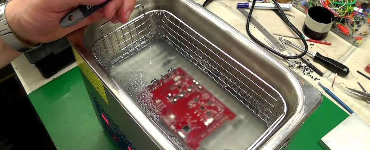
ยท Easy to clean

Another factor that makes FPC beneficial to use is that such a system is easy to clean. Now these connectors function with a special cable that connects with a conductive adhesive. Most of the FPCs are made of silicone. It means you can clean these silicone conductors completely with a brush. Make sure to handle them with care while cleaning to protect them from possible damage. 

The alternatives for cleaning these connectors include soft fabrics and spraying water to remove little fragments and debris. Do not leave any remains on the connector to ensure quality performance. Never use cleaning equipment containing detergents, as these are not appropriate for your LCD.

ยท Easy to connect

The FPCs are easy to connect as well. It means they consume less time for the assembly. You can easily connect critical panels with PCBs with the help of such connectors. Also, FCPs are important for bulky devices used in different domains. These include industrial machinery, consumer electronics, printing devices, and smartphones. 

ยท GPIO pins

These pins combine the sensors with the display system of your LCD. You can use LCDโ€™s original connectors, but using additional connectors like FPC makes you assemble it fastly. 

Wrap Up!

Now you can easily select the best interface for your LCD. In this post, we have discussed the drawbacks of each interface as well. It will help you in making a perfect choice for interfaces that will serve well in the long run. 

What Is Copper Clad Laminate (CCL)?

double sided copper clad board

Introduction

Copper clad laminate (CCL) is the fundamental building block material used in the fabrication of printed circuit boards (PCBs). CCL consists of a central insulating core laminated between layers of copper foil. The properties and quality of CCL have a major impact on the performance and reliability of completed PCBs. This article provides an in-depth overview of CCL technology, manufacturing processes, materials, properties, and applications.

CCL Basics

CCL provides the starting point for rigid PCB fabrication. The basic construction consists of:

  • Central insulating core layer
  • Copper foil laminated to one or both sides
  • The core is pre-impregnated (prepreg) with adhesive resin

The core gives mechanical support while the copper foil allows formation of conductive pathways by etching. The adhesive resin bonds the foil to the core.

Typical CCL Composition

Standard grades of CCL suitable for most PCB applications consist of:

  • Core: Woven fiberglass pre-impregnated with epoxy resin (FR-4 Grade)
  • Copper foil: 18um to 70um electrodeposited copper foil

The fiberglass reinforcement provides dimensional stability while the epoxy resin gives mechanical and dielectric integrity. Copper foil thickness is specified based on current density requirements.

CCL Fabrication Process

CCL undergoes an intricate fabrication process including:

  • Core preparation – Cutting, inspection, cleaning
  • Impregnation – Core material is dipped in resin solution
  • B-stage curing – Partial drying and semisolidifying the resin
  • Lamination – Foil application under heat and pressure
  • Autoclave curing – Fully cures resin to bond foil
  • Finishing – Cutting, machining, edge preparation

Precision controls during each phase ensure reliable, consistent CCL quality.

Applications of CCL

As the foundation of PCBs, CCL is utilized across all segments of the electronics industry:

  • Consumer Electronics – Phones, tablets, IoT devices
  • Computers – Server boards, workstations, laptops
  • Automotive – Engine controls, infotainment, radars
  • Aerospace and Defense – Avionics, weapons, navigation
  • Medical – Imaging systems, diagnostics, therapeutic devices
  • Industrial – Programmable controllers, test equipment
  • Telecommunications infrastructure

The properties and cost of CCL directly impact the capabilities and economics of these end products.

CCL Material Grades

CCL is formulated in many specialized grades to meet application requirements:

  • FR-4 – Flame retardant, standard grade for most commercial uses
  • High Tg – For higher temperature or thermal shock environments
  • Low Loss – For high frequency applications
  • High Speed – Optimized dielectric properties for fast digital signals
  • Halogen Free – For environmentally compliant PCBs
  • Aluminum Clad – Using aluminum instead of copper foil

There are over 100 defined CCL grades addressing specific thermal, electrical, and mechanical needs.

Key CCL Properties

Copper-Clad-Board-Material

CCL is engineered to deliver specialized properties based on chemistry and composition:

  • Dielectric Constant (Dk) – Impacts signal propagation delay and impedance
  • Dissipation Factor (Df) – Determines dielectric losses for high frequency boards
  • Dielectric Strength – Maximum voltage isolation capability
  • Thermal Conductivity – Heat transfer capability
  • Coefficient of Thermal Expansion (CTE) – Impacts thermal stress and reliability
  • Glass Transition Temperature (Tg) – Determines maximum operating temperature
  • Moisture Absorption – Critical for preventing electrical leakage

Properties are tuned through resin chemistry, core materials, and processing methods.

CCL Thickness

A standard thickness range for common CCL grades is:

  • Core only: 0.002โ€ to 0.062โ€
  • Copper clad: 0.004โ€ to 0.064″

Thickness uniformity is critical across a CCL lot. Thinner cores provide greater layer stacking density in multilayer PCBs.

Copper Foil Types

Several copper foil varieties can be laminated in CCL:

  • Standard ED Foil – For general applications
  • RA Foil – Rolled annealed, more ductile
  • VLP Foil – Very low profile with smooth surface
  • EF Foil – Electrodeposited fine grained foil
  • OF Foil – Oxygen-free foil for high frequency boards

Foil grain structure, roughness, and thickness impact costs and PCB fabrication processes.

CCL Supply Chain

CCL manufacturers produce raw copper clad sheets that get transformed into finished PCBs at board shops:

  • CCL Manufacturers – Fabricate base material in high volume
  • PCB Fabricators – Process CCL into finished circuit boards
  • Laminate Distributors – Provide inventory and delivery to PCB fabricators
  • OEMs – Source finished boards from fabricators

Reliable CCL properties and availability support PCB mass production for electronics supply chains.

CCL Considerations for PCB Designers

Key CCL parameters PCB designers should consider when specifying materials:

  • Dielectric Constant – Impacts signal propagation speed
  • Loss Tangent – Causes signal loss and degradation
  • Thermal Conductivity – Determines ability to dissipate heat
  • CTE – Impacts reliability and thermal stress tolerance
  • Moisture Absorption – Can reduce surface insulation resistance
  • Dk and Df Stability – Ensures stable electrical performance

Consulting your PCB fabricator during material selection ensures manufacturability and performance.

Conclusion

CCL forms the backbone of the PCB industry, providing the insulating structure onto which copper traces are etched. Engineering CCL for optimal electrical, thermal, and mechanical properties enables PCBs to serve reliably in diverse operating environments ranging from handheld devices to cutting-edge aerospace applications. Thanks to continual CCL innovations, PCB technology continues rapidly advancing to power todayโ€™s electronics innovations.

Frequently Asked Questions

Q: What is the difference between CEM-1, FR-4, and other CCL designations?

These denominations specify the resin system, glass fabric material, and flame retardance properties of the CCL. FR-4 uses brominated epoxy resin while CEM-1 uses a non-halogenated resin system. Different grades offer tradeoffs between cost, performance, and manufacturability.

Q: What are some key considerations when selecting copper foil type?

Key factors include foil thickness, ductility, profile roughness, grain structure, and compatibility with imaging processes. Thinner foils enable finer lines and spaces while roughness affects bond strength. Discussing requirements with your PCB fabricator ensures the optimal foil is chosen.

Q: What is the difference between woven and non-woven CCL?

Woven CCL uses fiberglass cloth with warp and weft threads held together by resin. Non-woven uses randomly arranged fiberglass strands evenly dispersed in the resin. Each construction offers different thermal and mechanical stability properties.

Q: How tight are the thickness tolerances held in CCL manufacturing?

Standard CCL thickness tolerance is ยฑ10% of the specified value. However, tighter tolerances of ยฑ3% or ยฑ5% are possible for high density designs where thickness uniformity is critical across layers.

Q: What is the difference between double-sided and multilayer CCL?

Double-sided CCL has copper foil on both sides of an insulating core for use in 2 layer PCBs. Multilayer CCL interleaves additional cores with adhesive to bond multiple layers for designing multilayer boards.

Rigid vs Flexible PCBs: Choosing the Right Type for Your Project

In today’s rapidly evolving electronics industry, the printed circuit board (PCB) serves as the backbone of virtually every electronic device. Whether you’re designing a smartphone, medical device, or industrial control system, selecting the appropriate PCB type can significantly impact your product’s performance, reliability, and cost-effectiveness. The two primary PCB categoriesโ€”rigid and flexibleโ€”each offer distinct advantages and limitations that must be carefully considered during the design phase.

This comprehensive guide explores the fundamental differences between rigid and flexible PCBs, their unique characteristics, applications, and the key factors to consider when determining which type best suits your specific project requirements.

What is a Rigid PCB?

Definition and Structure

A rigid PCB is the traditional, non-bendable circuit board that has been the industry standard for decades. These boards consist of a solid substrate material that maintains its shape under normal conditions and provides a stable platform for mounting electronic components.

The typical structure of a rigid PCB includes:

  • A rigid substrate base (commonly FR-4 epoxy glass)
  • Copper layers for conductive pathways
  • Solder mask to protect copper traces
  • Silkscreen for component identification and reference designators

Common Materials

The most widely used material for rigid PCBs is FR-4 (Flame Retardant-4), a glass-reinforced epoxy laminate that offers excellent electrical insulation properties, mechanical strength, and relatively low cost. For specialized applications, other materials may be employed:

  • FR-1 or FR-2 (phenolic and paper laminates) for simple, low-cost applications
  • Ceramic substrates for high-frequency or high-temperature environments
  • Metal core PCBs (aluminum or copper) for enhanced thermal management
  • High-Tg FR-4 for improved thermal reliability

Typical Applications

Rigid PCBs dominate numerous markets due to their durability, ease of manufacturing, and cost-effectiveness. Common applications include:

  • Consumer electronics (computers, televisions, gaming consoles)
  • Industrial machinery and control systems
  • Automotive electronics and engine control units
  • Power supply units and high-voltage equipment
  • Telecommunications infrastructure
  • Military and aerospace systems requiring high reliability

Pros and Cons

Advantages of Rigid PCBs:

  • Cost-effective for standard applications
  • Excellent mechanical stability and durability
  • Supports high-component density
  • Familiar design process with established manufacturing techniques
  • Better heat dissipation capabilities
  • Suitable for through-hole and surface mount components

Disadvantages of Rigid PCBs:

  • Cannot be bent or flexed
  • May require more space in compact devices
  • Limited design flexibility for complex 3D applications
  • Potentially heavier than flexible alternatives
  • May require additional interconnection methods

What is a Flexible PCB?

Definition and Structure

Flexible PCBs (also known as flex circuits) are thin, lightweight circuit boards designed to bend, fold, and flex during installation and operation. Unlike their rigid counterparts, flex PCBs can conform to three-dimensional shapes, making them ideal for applications with space constraints or dynamic movement requirements.

The typical structure of a flexible PCB includes:

  • A flexible substrate base (commonly polyimide)
  • Thin copper conductors
  • Coverlay (specialized flexible solder mask)
  • Optional stiffeners for component mounting areas

Materials Used

The primary substrate material for flexible PCBs is polyimide (such as DuPont’s Kaptonยฎ), which offers excellent electrical properties, temperature resistance, and mechanical flexibility. Other materials in flex PCB construction include:

  • Adhesives for bonding copper to the substrate
  • Coverlay materials (polyimide or polyester) for protection
  • Selective stiffeners (FR-4, polyimide, aluminum) for component mounting areas
  • Specialized surface finishes suitable for flexible applications

Common Applications

Flexible PCBs excel in applications where space constraints, weight reduction, or dynamic flexing are critical factors:

  • Medical devices (hearing aids, pacemakers, implantable devices)
  • Wearable technology and fitness trackers
  • Foldable electronics and displays
  • Cameras and optical devices
  • Aerospace and satellite systems
  • Automotive applications (dashboard electronics, sensors)
  • Dynamic flex applications (disk drives, printers)

Pros and Cons

Advantages of Flexible PCBs:

  • Can be bent, folded, or flexed to fit tight spaces
  • Significantly reduced weight and thickness
  • Elimination of connectors and wiring harnesses
  • Better resistance to vibration and mechanical stress
  • Enhanced packaging capabilities for 3D applications
  • Improved thermal management in certain configurations

Disadvantages of Flexible PCBs:

  • Higher manufacturing costs compared to rigid PCBs
  • More complex design rules and constraints
  • Limited component density in flexible areas
  • Specialized handling requirements during assembly
  • Potential flex fatigue in dynamic applications
  • Less standardized manufacturing processes

Key Differences Between Rigid and Flexible PCBs

Understanding the fundamental differences between rigid and flexible PCBs is essential for making informed design decisions. The following comparison highlights the most significant distinctions:

Material Composition and Physical Properties

FeatureRigid PCBFlexible PCB
Base MaterialFR-4, ceramic, metal corePolyimide, polyester
Thickness1.5mm-3.0mm typical0.1mm-0.2mm typical
FlexibilityNoneHigh (can bend 90ยฐ or more)
WeightHeavierSignificantly lighter
Thermal ExpansionHigher coefficientLower coefficient
Vibration ResistanceLowerHigher

Design Flexibility and Constraints

Rigid PCBs conform to a two-dimensional plane, limiting their application in complex three-dimensional spaces. In contrast, flexible PCBs can be designed to fit virtually any three-dimensional shape, enabling innovative form factors and integration possibilities.

However, flex PCB designs must carefully consider bend radii, neutral axis positioning, copper trace orientation, and other mechanical factors that aren’t typically concerns with rigid designs.

Durability and Reliability

While rigid PCBs excel in applications requiring structural stability and component support, flexible PCBs often demonstrate superior durability in environments with vibration, shock, or thermal cycling. The lack of rigid interconnections and the ability to absorb mechanical stress contribute to the enhanced reliability of flex circuits in dynamic applications.

Cost and Manufacturing Complexity

Rigid PCB manufacturing is a mature, highly standardized process with lower material costs and fewer specialized requirements. Flexible PCB production involves more specialized materials, tighter process controls, and often more complex handling procedures, resulting in higher overall costsโ€”particularly for low-volume production.

FactorRigid PCBFlexible PCB
Material CostLowerHigher
Tooling CostLowerHigher
Process ComplexityStandardSpecialized
Minimum Feature SizeLargerSmaller
Production TimeShorterLonger
Volume Price BreakReaches lower costs at lower volumesMay require higher volumes for cost efficiency

Rigid-Flex PCBs: A Hybrid Solution

Combining the Best of Both Worlds

Rigid-flex PCBs represent a hybrid approach that integrates rigid board sections with flexible interconnections in a single, unified structure. This technology combines the stability and component-mounting capabilities of rigid PCBs with the space-saving and dynamic benefits of flexible circuits.

The construction typically involves:

  • Rigid sections built with FR-4 or similar materials
  • Flexible sections using polyimide
  • Specialized lamination processes to bond the different materials
  • Careful layer stack-up planning to manage stress points

Benefits of the Hybrid Approach

Rigid-flex technology offers numerous advantages in complex electronic applications:

  • Elimination of connectors between board sections
  • Enhanced reliability through reduced interconnection points
  • Optimized space utilization in three-dimensional environments
  • Improved signal integrity with shorter, controlled-impedance paths
  • Simplified assembly processes
  • Reduced overall system weight

Use Cases and Applications

Though typically more expensive than either rigid or fully flexible options, rigid-flex PCBs excel in high-reliability applications where failure is not an option:

  • Aerospace and satellite systems
  • Military and defense electronics
  • Medical implantable devices
  • High-end consumer electronics (smartphones, wearables)
  • Automotive safety systems
  • Industrial automation equipment

Read more about:

Choosing the Right PCB Type for Your Project

Shengyi WLM1 PCB

Selecting the optimal PCB technology requires careful consideration of various project-specific factors:

Mechanical Requirements

  • Space constraints: If your application has severe space limitations or requires conforming to a non-planar surface, flexible or rigid-flex PCBs may be necessary.
  • Dynamic movement: Applications requiring repeated flexing during operation (like folding displays or moving parts) typically demand flexible circuits.
  • Structural support: If the PCB provides structural integrity to the device, rigid boards usually offer superior performance.

Electrical Performance Needs

  • Signal integrity: High-frequency applications may benefit from the controlled impedance capabilities of either rigid or flexible designs.
  • Power handling: Heavy copper requirements for high-current applications are generally easier to implement on rigid PCBs.
  • Thermal management: Heat dissipation requirements may dictate PCB type selection, with metal-core rigid PCBs offering advantages for high-power components.

Environmental Considerations

  • Temperature extremes: Both rigid and flexible PCBs can be designed for high-temperature environments, but material selection becomes critical.
  • Vibration and shock: Flexible circuits generally provide superior resistance to mechanical stress.
  • Chemical exposure: Material compatibility with environmental conditions must be evaluated.

Budget and Timeline Constraints

  • Production volume: Higher volumes can justify the increased tooling costs associated with flexible PCBs.
  • Development budget: Rigid PCB prototyping is typically more cost-effective for initial design validation.
  • Time-to-market: Rigid PCB manufacturing generally has shorter lead times and more widely available fabrication services.

Design and Manufacturing Considerations

Design Rules and Requirements

Designing for rigid versus flexible PCBs involves different considerations and constraints:

Rigid PCB Design Guidelines:

  • Standard trace width and spacing guidelines based on current requirements
  • Via technologies selected based on layer count and density needs
  • Component placement optimized for assembly and testing access
  • Thermal relief patterns for ground planes and power connections

Flexible PCB Design Guidelines:

  • Rounded corners for all trace routes to prevent stress concentration
  • Traces routed perpendicular to bend lines where possible
  • Staggered trace arrangements in flex areas to distribute stress
  • Additional clearances around plated through-holes in flex regions
  • Coverlay openings designed with fillets to prevent delamination

Manufacturing Challenges

Each PCB type presents unique manufacturing challenges:

Rigid PCB Manufacturing Considerations:

  • Standard manufacturing processes with high industry familiarity
  • Wide availability of fabrication houses with competitive pricing
  • Established quality control and testing methodologies
  • Standardized material availability

Flexible PCB Manufacturing Considerations:

  • Specialized handling equipment required
  • More complex lamination and drilling processes
  • Tighter material and process controls needed
  • Limited number of manufacturers with full capabilities
  • Special tooling often required for complex designs

Cost Implications

Cost factors vary significantly between PCB types:

  • Material costs: Flexible circuit materials typically cost 3-5 times more than standard FR-4.
  • Engineering time: Flexible and rigid-flex designs often require more design hours.
  • Tooling costs: Flexible PCB tooling is generally more specialized and expensive.
  • Production runs: Larger volume production can offset the higher initial costs of flexible circuits.
  • Assembly costs: Rigid PCBs typically have lower assembly costs due to standardized processes.

Common Mistakes to Avoid

Application Mismatch

One of the most expensive errors is selecting an inappropriate PCB type for the application:

  • Using flexible PCBs where rigid boards would be more cost-effective
  • Attempting to implement a rigid design in applications requiring flexibility
  • Over-engineering with rigid-flex where simpler solutions would suffice

Design Oversights

Common design pitfalls include:

  • Ignoring bend radius limitations in flexible circuits
  • Failing to account for flex fatigue in dynamic applications
  • Improper component placement relative to bend areas
  • Inadequate strain relief at transition points in rigid-flex designs
  • Incorrect stack-up planning resulting in neutral axis misalignment

Manufacturing Preparation Errors

Preparing manufacturing data incorrectly can lead to costly mistakes:

  • Insufficient documentation of bend requirements
  • Missing bend line indicators on fabrication drawings
  • Inadequate specification of material requirements
  • Unclear layer stack-up definitions for rigid-flex designs
  • Improper panelization for efficient production

Conclusion

The choice between rigid, flexible, or rigid-flex PCB technology is pivotal to the success of any electronic product. Each type offers distinct advantages that must be carefully weighed against project requirements, constraints, and objectives.

Rigid PCBs continue to dominate the market due to their cost-effectiveness, ease of manufacturing, and suitability for a wide range of applications. Flexible PCBs provide unique solutions for space-constrained, lightweight, or dynamic applications where traditional rigid boards fall short. Rigid-flex technology bridges the gap between these options, offering enhanced reliability for mission-critical systems where failure is not an option.

Ultimately, the most successful PCB selection process involves thorough analysis of mechanical, electrical, environmental, and economic factors, coupled with early collaboration between design, manufacturing, and assembly teams. By understanding the fundamental differences between these PCB types and their respective strengths and limitations, designers can make informed decisions that optimize their products for performance, reliability, and cost-effectiveness.

FAQs

What is the fundamental difference between a rigid and flexible PCB?

The primary difference lies in the base material and physical properties: rigid PCBs use stiff substrates like FR-4 that maintain their shape, while flexible PCBs use thin, bendable materials like polyimide that can conform to three-dimensional shapes and withstand dynamic flexing.

Is a flexible PCB more expensive than a rigid one?

Yes, flexible PCBs typically cost 30-50% more than comparable rigid PCBs due to more expensive raw materials, specialized manufacturing processes, and more complex handling requirements. However, they may reduce overall system costs by eliminating connectors, reducing assembly steps, and enabling more compact designs.

When should I use a rigid-flex PCB?

Rigid-flex PCBs are ideal for applications requiring high reliability, reduced weight, and complex three-dimensional packaging where traditional interconnection methods would create reliability issues or take up too much space. Common applications include aerospace, medical devices, and high-end consumer electronics.

Can flexible PCBs be used in high-power applications?

While flexible PCBs have limitations regarding thermal dissipation compared to metal-core rigid PCBs, they can be designed for moderate power applications by incorporating techniques such as wider traces, additional copper weight, strategic use of stiffeners, and thermal management features. For very high-power applications, rigid or metal-core PCBs typically remain the preferred choice.

How does the design process differ between rigid and flexible PCBs?

Flexible PCB design requires additional considerations including bend radius limitations, neutral axis calculations, trace routing relative to bend lines, specialized material stack-ups, and dynamic stress analysis. Designers must also specify coverlay openings rather than traditional solder mask and may need to incorporate stiffeners for component mounting areas.

Use Vias On Pads for Designing and Manufacturing PCBs

vias on pads

Via stands for Vertical Interconnection access. Vias help in transferring signals from one layer to another layer of a PCB. Let’s suppose the tracks exist on the x-axis and the y-axis of a PCB while vias are present on the z-axis. Generally, they consist of tiny vertical pipes with a coating of conductive layer and put in holes. These holes also use different kinds of filling, which ensure high electrical and mechanical strength.

In a traditional method, if a pin is used to connect vias, it creates tracks that help in routing the signal far away from the pads. Moreover, this method does not suit well for Surface-mounted dense PCBs, BGAs, ICs, and QFN.

This article helps in understanding the Via-in-pad in detail. It describes the vias types depending on their depth. Moreover, this article will surely help you in understanding the development and usage of via-in-pad in various devices and applications.

Introduction

Gordon Moore, the CEO of Intel, in 1956, indicated that the use of transistors in one silicon chip would double every couple of years. However, it was only the beginning. Over the passing years, the component size keeps decreasing.

However, in the late 1980s, the innovation of I’d and the constantly decreasing size of electrical components gave rise to the uselessness of manually designed PCBs. This led to the manufacturing of PCBs with multilayer, flexible variants and high power to boost efficiency.

Printed Circuit Board offers a platform and mechanical support to place components over them and create a connection between them. Copper tracks help in creating connections between components in a single-sided PCB while it needs via for transferring signals from one surface layer to other surface layers.

Different Types of Vias On Pads

Via in PCB

Vias come in variant forms depending on their usage and the type of connections they create. Let’s dive into the details of some most commonly utilized vias.

1. Through-hole Via

Through-hole via helps in shorting almost all PCB layers at a certain point. It creates a hole through drilling and then uses conductive copper to coat it. This helps in connecting all PCB layers from the outer layer to the other outer layer, all from top to bottom. 

Because of its simple construction and structure, through-hole vias come in the most common category in the manufacturing of a PCB. Among all types of vias, through-hole vias are the simplest and cheapest to create.

However, a revolution in the advancement of accurate machines developed special types of vias that allowed designers to leave certain layers of a PCB. These specialized vias comprise buried, blind, via-in-pad, and microvia.

2. Blind Via

Blind Vias help in creating connections between the external layer and more than one internal layer. These types of vias can only be visible from one side while invisible from PCBs’ other side because blind via cannot go through the whole PCB. This gives them their name. 

Blind via seems more expensive and complicated to make than through-hole via.

3. Buried Via

Buried Vias help in connecting more than two internal PCB layers. These types of vias do not make connections with the external layer. Thus, one cannot see it from the outer side. Buried vias are only used over the surface of a PCB with more than four layers. This also makes it more difficult to create them than blind vias.

4. Microvia

Microtia refers to traditional vias but in small sizes with certain changes in the structure. Microvias give a similar look to a frustum instead of creating a cylindrical shape. The radius of a micro via keeps decreasing with its transitioning from one PCB layer to the other.

Designers create micro vias to specifically connect two or more layers. However, for creating connections of multilayer PCB, manufacturers place micro vias over the top of one another and stack them. Buried micro vias typically use filling like epoxy conductive substances, which enhance their durability from mechanical pressure and stress.

What Is A Via In Pad?

Via-in-pad, as the name suggests, is put inside the pad of electronic components on the PCB surface. They create connections between external layers to all other PCB layers.

However, to understand the Via-in-pad necessity in a PCB, let’s dive into applications with high-frequency and HDI PCBs that use ICs along with a package of BGA.

Applications of Vias On Pads

PCB designers mainly use vi-in-pads in the manufacturing of PCBs when saving space concerns them the most. Via-in-pad is also widely used with tiny BGA package components as they do not allow other vias to fit in it. 

Moreover, BGA packages help in fixing and placing the tiny and compact surface-mount components with various amounts of pins. Components pins in the packages of BGA arrange in a systematic matrix order in which each pin has a tiny solder ball. Contrary to other widely used packages like Dual-in-line, the BGA package allows higher packing ruggedness and efficiency.

The solder ball size and the distance among the closeby BGA pins must be as tiny as a millimeter fraction. This makes the routing of surfaces complicated. Moreover, tracks with smaller trace widths are put out from each pin in an appropriate place for creating vias. Although, this does not seem to be an ideal approach.ย 

In electrical components in which the distance among the pins is smaller than the secure track clearance, then it may lead the PCB design system to give warnings. 

Regardless of routing all pins far away and creating a via away from an electrical component, you can directly put the via right under the BGA pad. This helps in carrying the signals through the pins of components to a specific layer of PCB.

 Advantages Of Vias On Pads Routing

Via-in-pad offers various benefits, which include.

ยท Space Saving

Saving space falls under the primary reason for utilizing via-in-pad in the PCBs. Regardless of sending signals away from a pad in traditional vias, via-in-pad makes a direct connection with the components under the pad. This leads to saving a lot of space. Moreover, it also eliminates the need to create dog-bone trails, which helps in routing optimization and significantly minimizes the whole footprint of a PCB.

ยท Easier Routing

Putting the via right beneath the pads directly not only save space on the PCB but also enables the process of routing simple. Particularly for tiny components with tiny footprints like the BGA package.

ยท Improved Heat Dissipation

Via-in-pad can effectively enhance the dissipation of heat for the power source, which mounts over the surface of a PCB. Nonetheless, putting a via closer to the heat or power source significantly enhances the thermal conduction between distinct PCB layers and components. Thus, it allows heat to dissipate faster.

ยท Reduce Parasitic Inductance

Via-in-pad helps in minimizing the associated inductance by eliminating extra connection parts. Additionally, via-in-pad also enables designers to put bypass capacitors nearby to the electrical components, which helps in reducing the inductance. Therefore, for high-speed interfaces and designs, it mainly helps in the enhancement of signal integrity.

Drawbacks of Vias On Pads Technology

FULL PCB MANUFACTURING Quote

Via-in-pad does have various downsides which affect the functionality of a PCB. Therefore, one must know them to create a functional and error-free PCB design. However, a PCB designer must go through these factors before considering any design for the via-in-pad. 

ยท Higher Manufacturing Cost

The creation of a via-in-pad mostly needs more than a hole drilling and filling it with a layer of conductive material. Via-in-pad needs a type of filling, especially conductive filling or conductive epoxy, to enhance its mechanical strength. However, this may add up in the cost because of the material and some additional steps of the assembly process. The price of via-in-pad manufacturing does not go down with an addition in the manufactured units, which literally increases the connected cost. 

ยท Surface Bumps

When the vias do not place and fill appropriately, it creates surface bumps. However, this surface regulation leads to complications in the components soldering process particularly in ting components with a clear connection. Therefore, while making via-in-pad, PCB manufacturers must make sure that surface bumps must be eliminated. 

ยท Increased Design Complexity

Via-in-pad is quite hard to install and design.

Conventional Vias Vs. Via-in-pad

Although the process of installation of via-in-pad is quite similar to the installation process of the traditional via. However, designers must consider a few factors while designing the PCB and its fabrication process. These factors include:

ยท Verifying PCB Manufacturerโ€™s Design Capabilities

Manufacturers of PCBs set up brief descriptions of their manufacturing process capabilities. However, before choosing a specific design of a PCB, a designer must go through the website of manufacturers to understand distinct parameters and factors. This includes the minimum size of an annular ring to prevent rule check of design or DRC and manufacturability design or DFM issues at the after stages.

ยท Extracting All The Required Files From The PCB Design Tool

Reviewing and evaluating the PCB design after exporting it from the EDA or Design Automation tool helps in solving issues and confusion. Additionally, the file which contains drill maps gives an extra file that contains a via-in-pad map. This ensures that conventional vias will not get filled and capped.

ยท Via Capping

Via tenting or capping is a type of coating process using a solder mask. This helps in resisting the solder paste or solder. Via tenting or capping does not consider an ideal choice for via-in-pad because solder masks cannot apply over pads. Therefore, while manufacturing PCBs, manufacturers need to create capped vias beneath the pad. This aids in preventing the solder mask from sliding inside the holes of the vias. For instance, in some cases, when vias are put beneath the thermal pad, this dissipates the heat better only if the via is uncovered or hollow.ย 

ยท Creating Precision Vias On Pads In Your Design

You may force the design systems of a PCB to insert vias inside the pad. However, this may lead to various checking errors of design rules if the system does not set up to a specific setting according to the technology. You have to ensure that the design software must support this sort of via-in-pad technology, then make a via according to it. After that, set all the necessary rules and configuration of the via-in-pad inside the design software. This helps the systems to accept vias as you inset them. 

To design an efficient design of modern PCBs, one may need a design system of a PCB. Make sure the system offers the necessary features to create various structures and shapes of vias. Also, it must have editing capabilities of rules to create your via-in-pad design. 

However, PCB designer Allegro serves as an ideal choice for this sort of work. It has advanced features via pad stack. Additionally, it owns a constraint editor and fully functions features of design rules. This also allows you to use any type of technology in creating the design of your PCB.

Conclusion

Vias are mainly used for transferring signals electrically between the various layers of a PCB. Via can be put directly under the pads instead of putting a conventional via, which keeps the signal far away from an electrical pin. Via-in-pad helps in saving space, enhances thermal conduction, minimizes parasitic inductance, and simplifies routing.

These types of via cost much more than traditional ones. Therefore, a PCB designer needs to check the manufacturer of PCBโ€™s design capabilities and make sure that they have all the necessary resources, advanced methods, and design tools. So that they offer high-quality products in the end.

A Complete Guide to PCB Encapsulation

PCB Encapsulation

The process of PCB encapsulation has to do with the encapsulation or the filling of electronic assemblies using a compound to offer some protection from vibration and shock, contaminants like chemicals, moisture, and dust, and corrosion. The electronic process of plotting also ensures the protection of the components from any security threats like reverse engineering or tampering.

In contrast to conformal coating, PCB encapsulation is more robust and thicker, which helps in protecting the electronic assemblies from different tin whiskers and harsh environments.

What Does PCB Encapsulation Mean?

Another reliable method for offering protection to the PCBs from any external damage is referred to as PCB encapsulation. You can also call it PCB potting. From the name, encapsulation strives to surround your PCB rather than just adding coat to it. The casing or pot will be built over the printed circuit board and then the fluid will be poured in the casing, thereby sealing the PCB up.

Because they are two major component systems, the process of PCB plotting deals with the mixing of resin and the hardener. Doing this will create a form of chemical reaction, which creates the cross-linked polymer. In order to boost the performance, resin feature mineral fillers, which have greater viscosity. In addition, majority of resins are made to be VOC-free and cure only at room temperature. This is why, PCB coating sprays are not necessary.

Though it is possible to apply a casing of 0.5 mm, usually, they are much thicker than this. With an increase in thickness also comes a weight increase. This leads to higher expenses for each coating. Also, the components will get better protection as a result of the increase in thickness.

Pros

  • Useful for high-volume applications
  • Its dark color provides design security
  • Provides greater protection against chock damage and water

Cons

  • A significant increase in weight
  • More process steps
  • Costlier than the conformal coating

PCB Encapsulation vs Conformal Coating

expoxy potting & Encapsulation

Choosing between conformal coating and circuit board encapsulation isnโ€™t about which method is best, rather it has to do with which of them suits your needs. Concerning this, youโ€™ll consider:

  • The layout and the design of the PCB
  • Its individual components
  • The Use environmentโ€™s expected conditions

If youโ€™ll be exposing your device to very extreme conditions, choosing PCBA encapsulation will be a smart choice. This is because it provides additional protection benefits. These environments include power plants, mines, and manufacturing factories.

Moreover, if flexibility is the major goal, i.e. when dealing with consumer electronics, the better choice will be PCB coating. Electronic encapsulation has to do with offering protection to the electronic assembly using a compound as a form of defense from vibration and corrosion shock.

How to Perform PCB Encapsulation

PCB encapsulation or pcb plotting deals with sealing of the PCB in a thick resin layer that offers great protection from harmful chemicals and physical shock. This process enhances the PCBโ€™s electrical performance.

To perform the PCB encapsulation,. You have to place your PCB assembly inside an open pot and then add some liquid compound in it till the entire PCBA becomes completely covered. This liquid has some hardener in it that helps to speed up the curing, and whenever this liquid solidifies, it plays a great protective role.

Normally, this resin utilized here is dark in color. This makes it very difficult for anyone to see that board under it. The materials commonly used for the plotting compounds include silicone, polyurethane, and pcb encapsulation epoxy.

Different materials come with their own benefits and pitfalls, which should be put into consideration. The applications determine your selection of the best material. For instance, pcb encapsulation epoxy and silicone work best for circumstances surrounding high temperatures. Moreover, urethane will offer a much better performance to chemicals. Therefo4e3, the most important point when choosing the materials is that you need to have a very good thought about the type of protection you desire.

When Should PCB Encapsulation be Used?

 As already mentioned, PCB encapsulation provides great protection performance. Therefore if you want your application or device to be able to stand against abrasion, strong physical shocks, high temperature, chemicals, abrasion, as well as moisture, PCB encapsulation should be the next move. This is because it also includes the vibration damping option.

Also, PCB encapsulation can help in protecting engineering privacy. This is possible due to its colored resin. This makes it difficult for the other people around to see the underneath board region and then make some profit from it.

However, this is a two-edged sword because this invisibility can bring in some obstacles when there is need for a rework or repair. Also, potting is important for all high volume work because it can be handled quickly on any assembly line. Finally, PCB potting provides a great aegis against all electrical arcs. Therefore, if you have high-voltage electrical devices, we advice that you make use of circuit board encapsulation rather than conformal coating.

What are the Benefits of PCB Encapsulation?

FULL PCB MANUFACTURING Quote
  • Encapsulation offers full protection against water damage and shock
  • It provides a well-secure seal that prevents contaminants from entering
  • It protects against chemicals and corrosion
  • A very reliable way of reducing RFI/EMI interference in different devices
  • Electronic components that are encapsulated provides a strong foundation for any wire bonding through the reduction of stress on the solder joints, which might have cause failure or breakage. This elimination of the exposed copper edges offers a reduced surface area for the oxidation. It also offers better adhesion between the solder pads and wires as well as better thermal performance.
  • Encapsulation helps to protect against tin whiskers which are harmful, by creating a form of environmental barrier.
  • It also prevents the components from getting destroyed or damaged because of external forces like mechanical vibration
  • It ensures the best functionality of the device over time. Also, it improves the insulation found between the electrical devices to help in reducing the loss of current
  • The reverse-engineer also finds encapsulated PCBs more difficult compared to those with conformal coating that are applied to some regions
  • Also, it protects the components from experiencing thermal expansion problems. Furthermore, it retains iconic purity as well as properties relating to moisture resistance
  • Generally, PCB encapsulation is faster and less expensive than the other methods of protection. This is because it needs few application steps and doesnโ€™t need reassembling.
  • VOC-free options are available
  • Using the potting and encapsulation material  is easy, even when using high-volume applications

What are the Applications of Encapsulation?

Encapsulation is applicable in different areas. These include photonics encapsulation as well as its use in cables.

PCB Encapsulation

Encapsulants are useful for protecting electronic components like PCBs that may experience damage as a result of moisture, mechanical vibration, as well as other environmental factors.

Offers Protection to Electronic and Electrical Components

Encapsulation provides protection for the electronic and electrical components from dust, dirt, water, as well as other contaminants.

Photonics Encapsulation

The encapsulated components are useful in applications including photonic integrated circuit, manufacturing of LEDs, solar panels, and fiber optics. Enclosures for optical instruments benefits from the utilization of electronic encapsulants. Also, they offer protection to the optical elements from any corrosion as well as prevent humidity and particles of dust from having any interference with the performance.

Also, LCDs require some defense against any light interference as a result of ultraviolet radiation. This is why they have to be encased in the encapsulant material. This helps in blocking UV rays coupled with maintaining a clear and a viewable surface area.

Cables

At times, the encapsulants are utilized on different electrical cables like twisted or coaxial pairs. They could get damaged easily due to oxidation and several environmental factors. Even, it protects the inner wires from exposure to moisture, chemicals, sunlight, or contaminants, as they could affect the performance.

What are the Required Materials for Encapsulation?

Conformal Coating

Materials involved in the process of circuit board encapsulation include adhesives, potting compounds, and resins. The resins usually coat the electronic devices during the electronic assembly. This helps in protecting them from environmental contaminants or water. You may need adhesives during the attachment of the encapsulating material that is found around the devices for protection.

This potting compound serves as an extra layer of protection for the electrical components. It also ensures heat dissipation through the conduction of excess thermal energy away. This prevents the extreme rise of temperatures beyond the normal range that can cause component failure.

Conclusion

One technology you must have if you wish to prolong your PCBโ€™s lifetime as well as reduce repair cost is PCB encapsulation. However, there is a need for deep consideration when choosing the best technology for your PCB projects as conformal coating and potting are two complex processes. They are also full of variables, which may have an effect on the final cost. However, if you have some doubts, then there is a need to consult professionals in the field to help you out. They will have to consider all the aspect of the project, budget, application, turnaround time, etc. to be able to make the best choice for you.

A Comprehensive Guide to CABGA (Chip Array Ball Grid Array)

CABGA

CABGA or Chip Array BGA or CA Ball Grid Array serve as a packaging technology. It is mainly used in microprocessors and Integrated Circuits or ICs.

In the packaging of CABGA, the IC, thus mounted over the ceramic substrate, surrounded with various tiny solder balls. However, the package arranges these solder balls in a pattern of grid array over the bottom surface of a package. They usually create connections between the PCB and the IC.

The package of CABGA gained popularity because of its high reliability, high thermal conduction, and greater pin count. These features make this technology ideal to use in devices that need high processing performance and high speed, like networking, advanced computing, and telecommunications.

Structure Of CABGA (Chip Array Ball Grid Array)

The technology of CABGA packaging’s structure comprises a ceramic substrate. It gives a strong and stable base alloy to the IC, with a greater number of ting solder balls. The package arranges these solder balls in the form of a grid pattern over the bottom surface of the package.

However, ceramic substrate incorporates the IC over it using flip-chip or wire bonding technology. At the same time, tiny solder balls help in creating a connection electrically between the surface of the PCB on which it is mounted and the IC.

Moreover, the number of solder balls number in CABGA packaging may vary from hundreds to many thousands based on the certain requirements of an IC.

Advantages Of CABGA (Chip Array Ball Grid Array)

BGA Chip

Chip Array BGA or CABGA is a type of packaging technology. It has gained popularity in the consumer electronics industry because of its great advantages and features. This section gives you a detailed insight into the major features of advanced CABGA packaging along with their usage in a vast range of devices.

1. High Pin Count

The technology of CABGA packaging has the ability to provide support to higher pin counts. This is considered among the main aspects. CABGA packaging contains tiny solder balls which provide high-density interconnections between the surface of the PCB and the IC. This feature of CABGA packaging makes it ideal for high-performance devices like advanced ICs, microcontrollers, and microprocessors that need a great number of I/O or Input/Output pins.

2. High Reliability

CABGA packaging also offers another important yet essential feature of high reliability. The packaging of CABGA comprises a strong ceramic substrate which gives a reliable and stable base alloy for an IC bga. At the same time, the solder balls of this package give a strong and reliable mechanical link between PCB and an IC. These amazing features enable CABGA packaging, an ideal choice for use in devices that need high reliability, like telecommunications, automotive electronics, and networking.

3. High Thermal Performance

CABGA offers another amazing feature of high Thermal conduction. This new technology of CABGA packaging contains tiny solder balls which give low heat resistance track from an IC to a PCB. Thus, helping in efficient heat dissipation. This capability proves helpful in high efficient ICs and microprocessors that produce heat in large amounts.

4. Cost-Effective

The latest technology of CABGA is considered to be the most cost-effective than other packaging types, which include DIP or Dual-in-line and PGA or pin-grid-array package. Moreover, the manufacturing process of CABGA packaging needs less material which takes less labor work. Thus, this turns it into an ideal option for various manufacturers concerned about reducing costs.

5. Ease Of Testing & Inspection

Another significant benefit of CABGA packaging is that it gives easy inspection and testing. CABGA packaging contains tiny solder balls which enable the inspection and test easily during the process of manufacturing. This function aids in ensuring that IC can work efficiently before shipping it to the customers.ย 

Applications Of CABGA 

FULL PCB MANUFACTURING Quote

The technology of CABGA packaging can utilize a vast range of reliable and high-performance devices like ICs, microcontrollers, and microprocessors. They need high thermal conduction, high reliability, and HD interconnects. Some main yet common application and usage of advanced CABGA packaging consists of the following:

ยท Telecommunication Equipment

Telecommunications equipment like switches, modems, and routers need really high-speed processing of data with reliable connectivity. This further ensures secure and fast transmission of data. The advanced technology of CABGA packaging is considered ideal for such devices because of its high reliability and greater pin count. This further helps in creating HD interconnects and smooth mechanical links between PCB and the IC.

ยท Networking Equipment

Network equipment like storage devices, data centers, and servers also need highly reliable connectivity and high-speed processing data to provide support to large-scale information processing and storage. Because of higher thermal conductors, manufacturers opt to use CABGA technology in these devices. This eventually dissipates heat in an efficient manner and provides ICs with stable functions under a greater workload.

ยท Computing Application

Computing applications with high-end computing clusters give high performance, and supercomputers need high-speed processing of data with high computational power. This manages the complex simulations and tasks. Due to high thermal conduction and greater pin count, manufacturers use this advanced high-tech CABGA packaging in these high-end devices. This, however, allows greater heat dissipation and high-density interconnections, which further enables the ICs to work efficiently under a great workload.

ยท Automotive Electronics

Automotive Electronics, like control modules of engines and systems of the latest driver-assistance, need high processing performance with high reliability, which ensures efficient and safe functionality of automobiles. Because of higher reliability, automobile devices opt to use this advanced CABGA package technology. However, this may ensure the ICs work smoothly under harsh conditions, which include vibration and high temperature.

ยท Medical Devices

Medical devices like CT scanners, MRI machines, and ultrasound machines need high-performance efficiency with high durability. This ensures timely and accurate treatment and diagnosis. Because of the high reliability, high pin count, and high-performance efficiency enables manufacturers to use CABGA packaging tech in medical devices. These features further allow the device to heat dissipation efficiently, have high-dense interconnects, and give stable functionality to the ICs for great workloads.

ยท Consumer Electronics

Consumer Electronics like smart TVs, mobile devices, and gaming consoles need high-speed processing of data, high-functional graphics, along with low consumption of power. However, this ensures efficient and smooth operation. The main reasons for CGBA incorporation in these devices consist of high thermal conduction, higher pin count, and cost efficiency. This enables the device for low production cost, efficient dissipation of heat, and interconnects with high density.

Conclusion

Chip Array Ball Grid Array, or CABGA, is considered a sort of advanced packaging technology. It is mainly utilized in high-functional microcontrollers, microprocessors, and ICs. It provides various benefits over other packaging technology types. This includes High reliability, pin count, thermal performance, and cost-efficient. 

How XC7A75T-2FGG484I Is Unique Form Rest of FPGAs?

Xilinx Zynq fpga

As technology advances, the need for faster and more powerful devices is increasing. Every day you have new technology and advancement in this field. FPGAs are one such revolutionary technology in the digital industry. It can adapt to different applications. The XC7A75T-2FGG484I is a remarkable FPGA from the Xilinx Artix-7 family. It is a great combination of technology and high performance.

In the following content, we will delve into the technical specifications of XC7A75T-2FGG484I. It will give you a clear understanding of its capabilities and features.

What Is XC7A75T-2FGG484I?

XC7A75T-2FGG484I is an FPGA from the Xilinx. Its family is Artix-7 family. FPGAs are easy to program or reprogram to perform specific functions.

The XC7A75T-2FGG484I is designed to provide high-performance processing capabilities, low power consumption, and low cost. It is a 7-series FPGA. In addition, it is built using 28nm process technology. This is the latest technology. As a result, you have compact, faster, and more power-efficient FPGA than. Let’s dig deeper to its

Specifications Of XC7A75T-2FGG484I

xilinx-spartan-7-fpga-1

The specifications of XC7A75T-2FGG484I are as follows:

 Logic Cells

The XC7A75T-2FGG484I has 52,160 logic cells; these are the basic building blocks of digital circuits. These cells are easy to program to perform specific functions. As a result, you can perform functions such as arithmetic and logical operations. In addition, data processing and signal conditioning are also easy with these logic cells. No FPGA is complete without these logic cells. This FPFA has a fairly good amount of logic cells. That’s why these are the building blocks of an FPGA.

Digital Signal Processing Slices

Digital Signal Processing, aka DSP slices, is again the main component of FPGA architecture. It has 180 Digital Signal Processing (DSP) slices. These DSP slices are specialized hardware blocks. That’s why they can perform complex mathematical operations.  For example, filtering, FFT, and multiplication. The DSP slices in XC7A75T-2FGG484I are optimized for many specific functions. They consume low power consumption and give you high performance.

Block RAM

Block ram is an essential part of FPGA architecture. There is no single FPGA that is complete without block Ram. BRAM is an abbreviation for Block RAM.

The FPGA has a total of 2.7 Mb of Block Random Access Memory. It is distributed across 68 individual blocks. The BRAM can store intermediate data and program code. As a result, it can be accessed with high-speed interfaces.

Clock Management

 You know that FPGA provides you with more precise control over systems and applications. That’s all possible due to the advanced clock management circuitry. It enables precise control and distribution of clock signals. In addition, it has four primary clock managers. Furthermore, each comes with four Phase-Locked Loops. As a result, they can generate and distribute clock signals with high accuracy. In addition, they also make sure there is low jitter.

Input and output Interfaces

The device features a wide range of Input and output interfaces. 34 General Purpose Input and output pins, 4 clock outputs, and 4 differential pairs make it a next-level FPGA. You don’t need to worry about its integration with other systems and devices. It has 16 high-speed transceivers, which make configuration and reconfiguration so easy. As a result, it supports various protocols. For example, PCIe, SATA, and Ethernet are some protocols. These adaptable input and output interfaces are simply great.                     

Advanced Power Management capabilities

XC7A75T-2FGG484I has advanced power management capabilities. As a result, it consumes low power without compromising performance. The device supports dynamic voltage and frequency scaling. As a result, you can adjust power consumption based on the workload. It is ideal for battery-operated devices. Most of the systems where powerย Conversations necessary, this FPGA suits the needs.

Breaking Down The Alphanumeric Code Of XC7A75T-2FGG484I

FULL PCB MANUFACTURING Quote

The alphanumeric code for XC7A75T-2FGG484I is a unique identifier for a specific FPGA. This model is manufactured by Xilinx. The code consists of a combination of letters and numbers. These codes, alphabets, and numbers are not ordinary. As a result, they provide information about the device’s specifications and characteristics. So if you know how to break down the numeric code, then you can easily have all the information.

Breaking down the  alpha numeric code:

  • XC7A75T shows the family name of the FPGA belongs. It is the Xilinx Artix-7 family.
  • 2 numbers indicate the speed grade of the device.
  • FGG484 package type, which refers to the physical package of the device. It is ball grid array package
  • The letter indicates the RoHS compliance status of the device.
  • The complete alphanumeric code for the XC7A75T-2FGG484I FPGA model is XC7A75T-2FGG484I. Moreover, now you can understand that these codes are not just ordinary numbers.

 Applications Of XC7A75T-2FGG484I

It is an advanced FPGA, so you can easily integrate it into modern devices in applications.

Following are the three major applications of this FPGA

Communication protocols and network

XC7A75T-2FGG484I FPGA is a versatile solution to implement complex communication protocols and network functions.  In addition, its potential is not limited to just encryption and 

Packet filtering. You can use it in quality-of-service (QoS) management systems. If there are creative designers, they can do wonders with it. As a result, you can see this FPGA part of many innovative devices.

Industrial automation

 In the domain of industrial automation, FPGAs have found their application in real-time control and monitoring functions. As a result, you can make it part of temperature sensing, motion control, and fault detection systems.

 Aerospace and defense

The aerospace and defense industry also benefits from the extensive utilization of this FPGA. As a result, you can see it is part of various applications like guidance systems and radar systems. In addition, it is also part of satellite communications. Similarly, there are several defense systems to have this FPGA.

Conclusion

If you are looking for an excellent FPGA for your next project, then XC7A75T-2FGG484I is a good choice. Its remarkable features and power management system make it suitable for different applications. It can easily integrate into other systems and applications. It comes in compact and sturdy packaging, so it is easy to carry or integrate.  Above all aake sure to purchase this XC7A75T-2FGG484I FPGA from a reliable vendor or distributor.

Technical Specifications, Features and Valuable Things About XC6SLX25-2FTG256C

Xilinx FPGA Chip

If you’re looking for a high-performance FPGA for your next project, the XC6SLX25-2FTG256C might be just what you need. This field-programmable gate array (FPGA) from Xilinx is designed for use in a wide range of applications, from digital signal processing to high-speed networking. In this article, we’ll take a closer look at the technical specifications of the XC6SLX25-2FTG256C, including its architecture, features, and performance capabilities.

ย What Is XC6SLX25-2FTG256C?

The XC6SLX25-2FTG256C is a member of the Spartan-6 family of FPGAs. They are known for their low power consumption and high Performance. With its advanced architecture and rich set of features, the XC6SLX25-2FTG256C is ideal for a wide range of applications, including:

Let’s take a closer look at the technical specifications of this powerful FPGA.

ย Unique Architecture

The XC6SLX25-2FTG256C features a six-input lookup table architecture. That’s why it is easy to do efficient logic implementation. It also includes abundant memory blocks, which enable you to implement a wide range of designs with ease. As a result, you can perform logical functions easily.

This FPGA supports a variety of Input and put standards, including LVCMOS and HSTL. Similarly, differential standards such as LVDS and RSDS. It also features advanced clocking and routing resources. Let’s dig deeper to know more about its technical specifications.

Features

Xilinx FPGA Programming

Some of the key features of the XC6SLX25-2FTG256C include the following:

  • This FPGA has 24,576 logic cells. These cells are the building blocks of any FPGA.
  • This Lookup Tables or LUTs 15,360. A LUT is essentially a small memory that stores a truth table for a specific logic function. That’s why these LUTs help in logic functions.
  • It has 30,720 Flip-Flops.
  • Block RAM of 432 Kb is just icing on the cake.
  • Maximum distributed RAM: 1.15 Mb is an added feature.
  • Four Clock management tiles are really helpful for power management.
  • This FPGA has 202 input and output pins. Similar Maximum differential Input and output pairs are 16.
  • The package type is FTG256C for this FPGA.

Break Down The Alphanumeric Code Of XC6SLX25-2FTG256C.

The alphanumeric code “XC6SLX25-2FTG256Cโ€™ pertains to a distinct variant of FPGA by Xilinx. If you have some technical knowledge of FPGA, then you can easily understand the alphabet and numbers in these part numbers. This alphanumeric code provides you with great knowledge about this distinct part number. As a result, you can easily understand the characteristics of this FPGA.

  • To break down the code, let’s start with the XC segment, which signifies that it is part of the Xilinx Spartan-6 family of FPGAs.
  • Moving on, 6SLX25 denotes the model number of this FPGA variant. As a result, you can understand its position within the Spartan-6 family. It also signifies its scale and competencies.
  • Furthermore, the -2 section of the code represents the speed classification of the device, wherein -2 suggests a moderate speed grade.
  • Additionally, FTG256 delineates the package form and the number of pins.
  • FT designates a fine-pitch ball grid array (BGA) package, whereas G256 indicates that it has 256 pins.
  • Finally, C reveals the RoHS compliance status of the device, where “C” indicates that it is RoHS compliant, meaning that it does not contain certain dangerous substances.

Support For Reconfiguration

You know that you can configure an FPGA. The good news is that you can easily do the reconfiguration.

 For this FPGA. It’s a bit complex, but it provides you more freedom to work with this FPGA. As a result, you can do better customization according to need. These features make the XC6SLX25-2FTG256C a powerful and versatile FPGA that can handle even the most demanding designs.

Impressive Performance With Maximum Operating

The XC6SLX25-2FTG256C offers impressive performance capabilities, with a maximum operating frequency of up to 400 MHz. It also supports high-speed serial connectivity up to 3.2 Gbps, which makes it ideal for applications that require fast data transfer rates.

The device also includes advanced power management features. That’s why it enables you to optimize power consumption. As a result, you can maintain high Performance. This makes it an ideal choice for battery-powered applications.  

High-Speed Serial Connectivity

High-velocity sequential interconnectivity for the XC6SLX25-2FTG256C pertains to its capacity to accommodate high-velocity sequential communication protocols. These standards encompass the Serial Peripheral Interface, Inter-Integrated Circuit, and Universal Asynchronous Receiver/Transmitter.

The XC6SLX25-2FTG256C FPGA can integrate with other devices or systems that utilize these protocols for communication. This enables swifter and more efficient data transmission. That’s why it is a pivotal factor in many high-capacity computing applications such as networking, video processing, and data storage.

Built-In System Monitoring and Debugging Features

FULL PCB MANUFACTURING Quote

The XC6SLX25-2FTG256C is packed with an array of hardware tools that allow users to efficiently monitor and debug their designs. Its built-in system monitoring and debugging features comprise:

The integrated Logic Analyzer tool facilitates the capture and analysis of signals within the FPGA. Similarly, Integrated ChipScope Pro is a powerful debugging and verification tool. It enables users to monitor and analyze the internal signals of their design.

The on-Chip Debug tool allows users to debug their design in real-time by setting breakpoints. As a result, the XC6SLX25-2FTG256C provides users with a comprehensive set of monitoring and debugging features.

Frequently Asked Questions

What Is the Maximum Operating Frequency Of The XC6SLX25-2FTG256C?

The XC6SLX25-2FTG256C has a maximum operating frequency of up to 400 MHz. Some factors like temperature and environment can affect this frequency.

What Is the Ideal Power Consumption of The XC6SLX25-2FTG256C?

You cannot describe the ideal power consumption for this FPGA. It depends upon various factors such as design, the working environment, and its self-built power management systems. Thatโ€™s why you cannot guess the ideal power consumption. 

Final Note

The comprehensive details of the XC6SLX25-2FTG256C FPGA’s technical specifications have been presented here. T its maximum operational frequency, embedded memory, and logic cells have been examined thoroughly. That’s why this FPGA is unquestionably powerful and multifaceted. As a result, you can effectively manage a broad spectrum of applications.

Whether you want to develop a complex digital system design or explore the possibilities of programmable logic, you can consider XC6SLX25-2FTG256C. Its superior attributes and Consistent Performance are certain to help realize goals and elevate projects to greater heights.

An Ultimate Guide to XC5VLX110-1FFG1153C FPGA

Xilinx Kintex fpga

Field-programmable gate arrays are gaining popularity due to their unmatchable properties. You can find several FPGAs in the market according to need. They have specific features and functionalities. That’s why it’s really hard to choose the best one. XC5VLX110-1FFG1153C is one of the best FPGAs. Let’s dig deeper to know more about this FPGA.

 What is XC5VLX110-1FFG1153C?

The XC5VLX110-1FFG1153C is a high-performance field-programmable gate array (FPGA). It is from Xilinx. You all know that Xilinx is a well-reputed company in making logic devices, especially FPGA.

The XC5VLX110-1FFG1153C FPGA is part of the Virtex-5 family of FPGAs. This family is well known for delivering high-performance computing solutions for a variety of applications. This XC5VLX110-1FFG1153C FPGA features a versatile architecture. As a result, you can configure it to meet a wide range of design requirements. High-speed communication and digital signal processing are examples.

XC5VLX110-1FFG1153C is built on a 65nm process technology and contains 110,160 logic cells. It is ideal for complex digital circuits. Moreover, it is easy to configure it.

ย Let’s dig deeper to know more about its specifications.

 Block Ram and Logic Cells

 Block ram and logic cells are the foundations of FPGA. The XC5VLX110-1FFG1153C FPGA boasts a highly sophisticated architecture that empowers designers to perform the task easily.   As a result, they can create intricate digital systems. Its flexible logic fabric can be effortlessly configured to implement custom logic functions, providing ample room for creativity and customization. With dedicated processing resources such as DSP slices and block RAM, this device is a powerhouse of digital design capabilities.

What’s more, the XC5VLX110-1FFG1153C FPGA features a whopping 1,872  KB of block RAM. It is greatly helpful for storage or as a scratchpad memory for temporary data storage. This is a significant advantage for designers and engineers. They always want to store large amounts of data. In addition, it is so helpful in quickly accessing temporary information. In addition, this FPGA includes 10 high-speed transceiver blocks. Delayed blocks can support data rates of up to 6.5 Gbps. As a result, it is a top choice for high-speed data transfer applications.

DSP Slices

ย This ideal FPGA contains 576 DSP slices. Mostly these are configurable blocks of hardware designed to perform specialized mathematical operations. In addition, DSP slices make data processing easy.

Clock Frequency

Maximum clock frequency: 800 MHz for this FPGA. That’s why it is ideal for use in a wide range of high-performance applications. You can do digital signal processing, high-speed communication, and image processing easily with it. In addition, the FPGA supports a wide range of communication protocols. PCI Express, Gigabit Ethernet, and Serial RapidIO are the best examples. That’s why it is ideal for use in networking and communications applications.

Ideal Operating Voltage

The operating voltage is 1.0 V. for this FPGA. It is highly ideal for all devices that are modern. All portable devices can use this FPGA. It consumes less power and works efficiently. So ideal for devices and systems looking for low-power solutions. When it comes to modern devices, power, and energy management are essential. This FPGA allows you to work efficiently.

Input And Output Pins

The XC5VLX110-1FFG1153C FPGA has 622 input or output pins. It’s a good number of pins. These pins play a crucial role in the construction of circuits and connectivity. These pins enable communication between diverse components by acting as the ears of the chip. As a result, signals or data from other sections of the circuit can be easily received. Conversely, output pins operate as the mouth of the FPGA. These pins transmit digital signals or data to other components like displays. As a result, these pins improve control.

It is essential to keep in mind that the specific functions of the input and output pins of the XC5VLX110-1FFG1153C chip may differ. It all depends on the overall circuit design and programming. Furthermore, it is critical to meticulously plan and design the circuit. As a result, you can utilize these input and output pins optimally and efficiently.

Why is it possible to use XC5VLX110-1FFG1153C?

FULL PCB MANUFACTURING Quote

The following are some key advantages of this FPGA. These are enough to tell you how it is ideal for all devices.

High-Speed Connectivity

FPGA has immense power, with a diverse range of high-speed connectivity options. It supports PCIe, Serial, and RapidIO. In addition, it also supports XAUI. These manifold connectivity options make the transfer of data possible. Faster data transfer renders this XC5VLX110-1FFG1153C FPGA the quintessential choice for a plethora of high-speed connectivity applications.

High-Performance Processing Capabilities

This FPGA also boasts high-performance processing capabilities. Thanks to its 576 DSP slices and 6.4 Mb of block RAM. This means that it can handle even the most demanding applications with ease.

Supple Configuration Scheme

This modern XC5VLX110-1FFG1153C FPGA also features a flexible configuration scheme. It allows designers to execute custom logic functions easily. They can easily configure this FPGA.

As a result, it optimizes performance for their specific application. This means that you can design the FPGA XC5VLX110-1FFG1153C to your needs. As a result, it performs exactly as you require. It means now you can customize its configurations according to need.

Efficient Energy Management Leads to Low Power Consumption

The best part of the XC5VLX110-1FFG1153C FPGA is its low-power operation. No doubt its impressive features are great. But its energy efficiency is appreciable. It is to choose the applications that require both high performance and energy conservation. So if you’re looking for a powerful and efficient FPGA, the XC5VLX110-1FFG1153C is the device for you

Wrap Up

The XC5VLX110-1FFG1153C FPGA is a progressive technology FPGA. It offers designers and engineers different unmatched features. Its unique capabilities and superior architecture make it a top choice for designers and engineers.   As a result, they can create complex digital systems and applications without complications. In my opinion, it is a great FPGA. Choose the XC5VLX110-1FFG1153C FPGA for your next digital design project.

You will experience the ultimate performance and flexibility. You can thank me later for letting me know about this FPGA.

No-Clean Flux vs. Water Soluble Flux: Which is the Best PCB Cleaning Agent?

No-Clean Flux vs. Water Soluble Flux

The presence of oxides and other unwanted materials on a PCBโ€™s surface potential impedes the performance. This is because the soldering process wouldnโ€™t be as smooth as it ought to be. A better way to tackle that is to use a cleaning agent. The choice is always between no-clean flux vs. water soluble flux.

The two have distinct features and their potential downsides. By comparing what they have to offer, you will arrive at a choice of the one that works best for you.

What is the Purpose of Flux for PCBs?

To better understand what the flux does for the circuit board, you first need to understand the reason for using it. The reason is that there are usually oxides or metal oxides on the PCBโ€™s surface. Among many other challenges, these oxides tend to make the bonding of copper difficult, as well as littering the surface.

It is therefore imperative to use a cleaning agent to get ride of those and prepare the PCBโ€™s surface for soldering.

By using a flux, you would be able to clean the PCBโ€™s metal surface, remove the oxides and further enhance the bonding or creating of a stronger solder joint.

Types of Fluxes for PCBs

There are two major types of fluxes or cleaning agents you can use. They are the no clean and water soluble flux.

They help you with cleaning the metal surfaces and to remove any of the oxides likely to interfere with the soldering process.

What is Water Soluble Flux Used for?

No Clean Flux soldering

Also called the organic acid flux, it is a type of flux used for cleaning the oxides off the PCBโ€™s surface. Unlike the rosin flux, it is made from organic materials other than rosin.

Why Use Water Soluble Flux?

There are a couple of arguments on the efficacy of water soluble fluxes, considering that they can leave behind some residues. Nevertheless, they have a good number of features that make them worth using.

These are some of the benefits or advantages of using a water soluble flux for electronics:

Highly Active

The highly active feature is the reason why this flux has a long life, when used in the process. It also aids the excellent soldering performance.

Excellent Cleaning

Due to the aggressive nature, the water soluble flux makes a good cleaning agent for wiping off metal oxides. This way, it prepares the circuit boardโ€™s surface for soldering.

Zero Burn-Off

Water soluble fluxes rarely burn off during the soldering process.

These are some of the additional reasons why you want to use the flux for your PCB:

  • It is made of high solid content, usually between 11% and 35%.
  • Halide free
  • Halide activated (pH neutral)
  • Halide activated (low pH)
  • It is occasionally solvent or water-based.

Downsides/Disadvantages of Water Soluble Fluxes

Here are some of the reasons why using this type of flux for getting rid of metal oxides is not recommended:

General Chemistry Aggression

This type of flux is generally aggressive and this often translates to corrosion. The fact that it remains even after soldering is a thing of concern because it can continue to react on the surface until it is fully wiped off.

Residue Deposition

Water soluble flux continues to react after soldering and this is primarily due to the residue it leaves behind. To this end, you must endeavor to wipe it all off.

Strenuous Removal Process

The process of removing the flux is not easy either. You must follow these processes to be sure the PCBโ€™s surface is freed of the flux:

  • Occasionally monitor the surface to find out if there are signs of ionic contamination. Sometimes, it is best to use either an Omegameter or Ionograph to test for this contamination.
  • Sometimes, the PCBโ€™s surface needs to be subjected to a machine-washing process to get rid of the lurking residue, faster. This often extends the lead time and causes additional expenses.

The Susceptibility to Dendritic Growth

The use of water soluble flux also exposes the board to dendritic growth. It infers to the metallic and hair-like growth that sprouts out between the short, adjacent conductor paths.

How to Use Water Soluble Flux

Despite the downsides, you can still maximize this PCB flux by washing it off as soon as the soldering process is over. If it still sticks, consider using the machine-washing process.

No-Clean Flux: What Is It?

FULL PCB MANUFACTURING Quote

It is the opposite of the water soluble flux, in the sense that it doesnโ€™t need to be washed off. No-clean flux are meant to be on the circuit boardโ€™s surface after the soldering process is over.

Also called the low-solids, it is the type of cleaning agent to use when you donโ€™t want to wipe off the PCBโ€™s surface after soldering.

The features of no-clean include:

1. Zero Cleaning

When we say that the no-clean flux doesnโ€™t need to be wiped off; it is because it leaves behind negligible residue. This means that the residue left behind is inconsequential and wouldnโ€™t harm the surface.

Besides, the composition of less chemistry and activity means that you might not need to clean the PCB after soldering.

2. Low-Solid Composition

The composition of low-solids means that the no-clean flux can be available in different types of liquids. For example, you could variants based on alcohol and water.

The choice of the one to use depends on the performance.

Downsides of No-Clean Flux

In comparing the pros and cons of no-clean flux, always check the amount of residue left behind, as compared to the possible infringement on the boardโ€™s performance.

With that being said, these are some of the potential issues with using a no-clean flux for your PCB:

Less Chemistry and Activity

While the presence of more chemistry and activity potentially increases the residue deposition; it could also impart the boardโ€™s performance.

In this instance, the reduction of the activity and chemistry of the no-clean flux makes it more difficult for the board to be soldered. The higher the activity and chemistry of the flux, the higher the soldering capabilities.

Residue-Related Failure

Although this type of flux boasts of leaving some unharmful, negligible residue behind, it is not entirely so. With the advent of new ways to manufacture modern electronics, and considering the closing of the gaps/spaces between these components; it has become expedient to get rid of residues.

The inability to do so often exposes the PCB to residue-related failures. Besides, the deposition of little residues varies by the assembly process. An example is the Through Hole Technology (THT) soldering process that requires the removal of all residues from the board.

Types of No-Clean Fluxes

Different types of no-clean fluxes exist. The following is an explanation of the different options available in the market, as low-solids:

1. Alcohol-Based and Rosin, Low-Solids/No-Clean Fluxes

This toes the line of traditional rosin fluxes, but with a bit of sophistication. This type of no-clean flux works well in the following aspects:

  • Low-heat applications
  • Preheat and long heat exposures and;
  • Higher heating processes

2. Alcohol-Based and Non-Resin, Low-Solids/No-Clean Fluxes

The removal of the rosin improves the volatilization capabilities of the active flux. They are best used for the applications that require minimal residues and less heat.

On the flipside, the non-resin, no-clean fluxes are susceptible to depletion, especially when subjected to the selective soldering process. This is due to the exposure to higher heat.

The best way to combat this is to either use a synthetic equivalent of rosin or leave behind a little flux of rosin to aid the encapsulation of the remaining ionic residues.

3. VOC-Free and Low-Solids/No-Clean Fluxes

These are water-based fluxes capable of handling more exposure to heat. The other features include being ideal for high-heat programs (due to the longer water evaporation time)): and the tendency to be a little more active.

On the flipside, using the VOC-free, no-clean flux is not advised due to the longer preheat cycle.

Why Should You Wipe-off the No-Clean Fluxโ€™s Residue?

soldering flux

Besides the fact that the little residue left behind could trigger residue-related failures; it is also likely to make the residues conductive.

Wiping the remaining residues on the PCBโ€™s surface after soldering also helps in the following ways:

  • It prevents the trapping of solder balls in the left-over no-clean flux, which is situated between the components and conductor paths.
  • Wiping-off the remaining residues helps to prevent leakage of currents between the circuits.
  • It aids the adhesion of the circuits to conformal coating.
  • Contaminations triggered by residue deposition are reduced.
  • It reduces the chances of moisture absorbing into the fluxโ€™s residue.

Key Considerations for Leaving Behind No-Clean Flux Residues

If you are still intent on not wiping off the remaining no-clean flux residues; here are some of the best practices to follow:

Low-Density Board Considerations

You may not encounter residue-related failures if the residues are left behind in the low-density or low-voltage PCBs.

No-Clean Flux Activation

The activation of the no-clean flux refers to the full temperature-cycling of the flux. This is often based on the solder profile from the solder pasteโ€™s manufacturer.

Hygroscopic Properties

Despite the activation of the fluxโ€™s residue, it is still likely going to be hygroscopic. The term refers to the fluxโ€™s residueโ€™s ability to absorb moisture, while prevent conformal coating adherence to the PCB.

No-Clean Flux vs. Clean Flux

While there are differences between the no-clean and water soluble fluxes, you may also want to compare it to another โ€“ clean flux.

A clean flux refers to the type of flux or cleaning agent that combines water, organic solvents and wetting agents.

The features include but are not limited to:

  • Consistency
  • The ability to remove solder paste residues, easily.
  • The clean flux is also notable for the improved wetting properties.
  • It also uses safer organic solvents, which have the EPAโ€™s approval.

On the flipsides, the clean flux might not be a good investment for getting rid of metal oxides on a PCB. It is so for the following reasons:

  • It requires extra cleaning, especially after the reflow process.
  • It also doesnโ€™t last if no-clean flux is used after it.

No-Clean Flux vs. Water Soluble Flux for Electronics

In choosing the right cleaning agent or flux for your circuit boards, a couple of factors are worth considering. Some of these are:

Consider the Service Environment

What type of environment or condition are you exposing the flux to? Ideally, the environment needs to be open or secluded, depending on what you are working on.

But, the point is that the type of service environment could be a โ€œbreeding groundโ€ for moisture. Besides, the following are also worth considering alongside the environment:

  • The extent of the residue left behind
  • The components’ density. Ideally, a circuit board with higher residue and more component densities is likely to be exposed to moisture than the one with little residue and a relatively low component density.
  • For the best results, use the no-clean flux for the standard service environments and the water soluble flux for the harsh environment.

The Assembly Process

For PCBs assembled via the Surface Mount Technology (SMT); use the no-clean flux. If the board uses the Through Hole Technology (THT); use the water soluble flux.

Consider the Applications

Where the circuit boards are designed for use plays an important role in choosing between water soluble flux vs. no-clean flux.

Using the water soluble flux for the high-risk applications is better, and this is due to the affordable re-optimization and less time spent.

Component Standoff Height

The Component Standoff Height (CSH) refers to the height of the components. The rule of thumb is to use the water soluble flux for the higher CSH.

The following are some of the best practices for the Component Standoff Height:

  • Avoid the use of water soluble flux with shorter components. This is because of the partsโ€™ susceptibility to trigger solder voids, trapping of the flux activators and the potential for causing short-circuiting.
  • The best way to determine the Component Standoff Height (CSH) is to compare both the soldering reflow profile and the bond pad.

Conclusion

The choice between the no-clean and water-soluble fluxes depends on the types of applications, the cleaning process and the circuit board componentsโ€™ densities. You should also reach out to a professional PCB assembling company to help you fine-tune and smoothen-out the grey areas so you can make a better decision.