A Comprehensive Overview of Thermistor Circuit: Principle, Types, and Diagram

Thermistor Circuit

Physics remains inadequate if you don’t talk about thermistors. Well, these remarkable devices, thermistors, are the invention of Michael Faraday, who brought this concept to light. He invented the first thermistor in the year 1833. A thermistor is a hybrid of a thermal and a resistor. The common thermistor is an RTD which is highly sensitive to temperature. There are some fantastic features of thermistors that we are going to decode the science behind thermistors through this post for you! So wake up that physics nerd inside you and join us to discuss thermistors right now!

Basic Principle of Thermistor Circuit

Thermistors work on a basic principle so that the devices can work at their finest without any disturbance. 

  • A thermistor is not a metallic device and works as a resistor and has a similar working phenomenon to a semiconductor with a negative resistance.
  • The resistance of thermistors directly depends on the temperature. Higher temperatures mean more resistance.
YouTube video

Parts Of Thermistor Circuit

Thermistors cannot survive without some crucial components of their work:

  • A special metallic tube that contains sensors inside a thermistor.
  • A fine insulative layer that divides the thermistor from the metal tube.
  • A wiring network made from lead that extends out from thermistors.

Different Types of Thermistor Circuits

Thermistor Circuit Board

We are going to explain about common types of thermistors:

Negative temperature Coefficient or (NTC) Thermistor Circuit

  • In an NTC thermistor, the resistance and temperature are inverse to each other. 
  • These thermistors are highly sensitive to even a slight change in temperature therefore these are reliable for censoring temperature changes in the devices. 
  • You can trust a thermistor when you need to record the temperature changes and amounts of currents.
  • It keeps the resistance low and lets more current pass through the system until it reaches an optimum level which is useful for the devices like fire censoring equipment, baking ovens, and ACs. 

Positive temperature Coefficient or (PTC) Thermistor Circuit

  • A PTC thermistor is directly proportional to the temperature. The resistance increases as you will increase the temperature. 
  • These are reliable for guarding the system against overcurrents that can lead to electrical fuses and glitches.
  • You align the PTC thermistors in a series circuit that helps to cope with the electrical fuses. 
  • There are two types of PTC thermistors, and we are going to have a deep look at these below:

Silistor Temperature sensor:

  • It has a silicon structure and follows a linear temperature graph for functioning. The resistance follows the temperature if it increases. 
  • These thermistors are not abundantly available in the market, but they are still existing.

Switching type Circuit

  • It is another type of PTC thermistor that sometimes acts as an NTC thermistor.
  • There is a specific temperature limit after which the nature of this thermistor just changes, like the colors of the sky. Now this temperature limit is known as Curie point. 
  • Some substances are more likely to undergo sudden changes in their nature when they cross Curie Point.
  • The resistance after crossing the Curie point also improves quickly. 
  • The fine applications of PTC thermistors are for small to midrange heaters, electric motors, and thermostats.

Disk & Chip Thermistor Circuit

  • Such thermistors have fine metallic contacts.
  • These often have lagging responses as compared to other variants.
  • The size of these thermistors is larger than the others.
  • A copper bar is important for maintaining the sensitivity of this thermistor on all counts.
  • It also offers impressive power dissipation, which is important for different devices. 
  • Due to the abovementioned features of this thermistor, it offers exceptional performance than bead thermistors. 
  • Such thermistors also offer exceptional endurance to tackle high levels of current. 

Epoxy Thermistor Circuit

  • You need an industrial-grade epoxy to solder it between the wires made of Teflon and PVC.
  • The size of these wires is small.
  • Due to their small size, these do not need extensive assembly procedures.
  • You can easily change the shape and position of these wires as well. 

Bead Thermistor Circuit

  • The wiring for bead thermistors works best if you use platinum.
  • You also need to connect them with the ceramic to improve the performance.
  • These thermistors are more reliable since they are fast with responses, offer more stability, and can handle extreme temperatures impressively. 
  • These thermistors are delicate in nature.
  • Since these are delicate and sensitive, a protective glass covering is important to conceal them.
  • Now, there is no need to worry since this covering does not create a negative impact on these thermistors at all. 

Glass Encapsulated Thermistor Circuit

  • These show efficient performance when you are talking about extreme temperatures. 
  • There is a glass layer that encapsulates these thermistors, thus named glass encapsulated thermistors.
  • These offer a higher degree of stability and also are reliable for adverse environmental changes. 

Probe Assemblies:

  • You use these thermistors probably every day in your life. Shocking, isnโ€™t it? Your geysers and air conditioners use probe assembly thermistors. 

Surface mount Thermistor Circuit

  • Such thermistors have important applications in the motherboards of consumer electronics like laptops and PCs. 

Composition and Structure of Thermistor Circuit

The shapes & designs of thermistors know no boundaries. Consumers use different types of thermistors for their personal use. In fact, industrial producers also rely on various sizes & shapes of thermistors as per the projects. These types include different materials for production as well. Iron, cobalt, and nickel are recommended materials that come in handy for the production of such thermistors. You need to grind the metallic oxides and change them into a powder-like form. 

After this, you will compact this powder which is called centering. It is this powder that lets you make different shapes of thermistors as per your requirements. Tools like probes are for shaping these thermistors into rod-like or bead-like thermistors. You also need to determine the temperature range of the application that you are making a thermistor. Different metals have different temperature ranges, which is why you need to make sure that your thermistor is the best fit for this application.ย 

Amazing Benefits of Thermistor Circuit

FULL PCB MANUFACTURING Quote

Thermistors give you multiple advantages in daily life. You are going to be grateful for this marvel of physics after reading these benefits below:

  1. Incubators used in the labs consist of thermistors for monitoring the temperatures of the samples.
    1. Thermistor is an affordable option to go for instead of other pricy temperature regulatory devices and sensors.
    1. Thermistors are easy and affordable to shape, which is why these are much more convenient to include in consumer electronics.
    1. Water cannot harm a thermistor at all, which is why it is safe to use around water and moisture.
    1. Lesser amount of current can prevent the thermistor from overheating.
    1. The properly developed thermistor, like the bead thermistor, has satisfactory strength.

Working & Testing of Thermistor Circuits

There are only two factors that hugely influence the performance of a thermistor. One is resistance, and the other is temperature. The resistance and temperature also influence each other and can change according to the situation. It is important to check the thermistors to ensure their fine performance. Some tools like an ohmmeter and a multimeter can help you with testing the thermistors. 

If you are using a PTC thermistor, just join its ends with the multimeter. Now heat up the sensor, and you will see that the resistor with resistance will start to increase. That proves you are testing a PTC thermistor since the temperature is directly proportional to the resistance in the case of a PTC thermistor. For NTC thermistors, the resistance will alleviate due to an inverse relation. 


Different Projects of Thermistor Circuits

Automatic fan Controller with Temperature Control

If you increase the temperature, it will turn the fan on.

You need the following components to successfully complete this project:

  • A Thermistor 
  • An industrial-grade resistor
  • A fan that is highly important for this project
  • A transistor 
  • A battery of 9V

Working

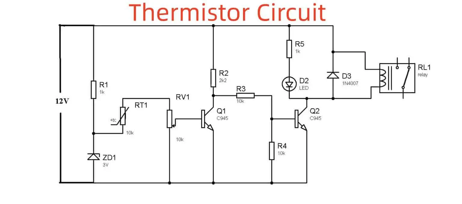
You need to construct a circuit that contains 10K ohm thermistors which are joined with 10K ohm resistors. We are using an NTC-type thermistor for this project. It means when you will increase the temperature, it will decrease the resistance. Now the thermistor includes a 10k ohm resistance, as we know. 

Now connect the fan with a transistor. Start heating the thermistor, and surely it will increase the temperature. When this happens, it will drive the resistance to decrease, which will turn on the fan. The contrary will happen, and it will switch off the fan when the temperature decreases. 

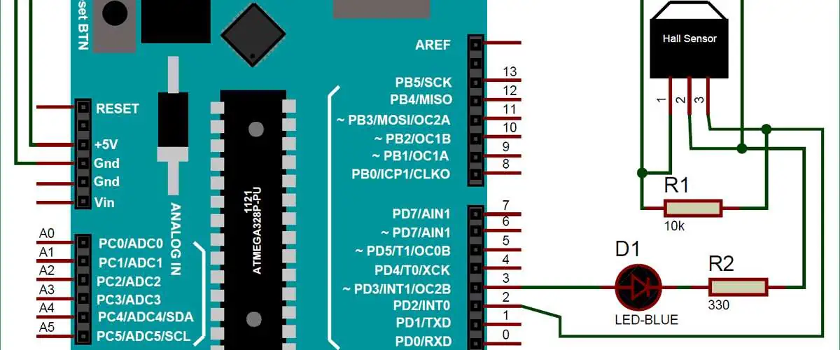
Specified Temperature Thermistor Circuit

We are now using an abThermistor & an amplifier (operational) for this project. Now this OP-AMP will act as a voltage comparator. Here is what you need to remember. Every amplifier (operational) can be a voltage changer, but every voltage comparator cannot be an OP-AMP. When we take LED1 and LED2, we will notice that the thermistor will record the resistance as per the temperature changes. More temperature means less resistance, and vice versa. 

The following components are important for this project:

  • Battery
  • Light emitting diode 
  • Lm-393 
  • Thermistor
  • Resistor

So we are working with two dividers for this project. You need to fix one divider and leave the other one as it is without fixing it. 

The fixed divider also has a fixed amount of resistance, and you can consider it as a reference voltage. The non-fixed divider has a thermistor that has a variable resistance. 

The OP-AMP will record the inputs of both these dividers. The job of the comparator is to keep comparing these inputs and minus one input from the different. 

Remember, we have not used any feedback loop for this project. The amplifier (operational) will follow saturation, and the output will remain lesser than 9V, which is the actual voltage of the battery that we are using in this circuit. Once you see the voltage approaching 9V, it will turn on LED 2, and when it approaches 0V, it will switch on LED 1. The LEDs will be not too bright since the amplifier (operational) does not interpret 0V because it is an ideal situation. 

The Essential Guide to Hall Effect Sensor Circuit – Working

hall effect sensor circuit board

The genius brain behind the Hall effect sensors is Edwin Hall. People loved his invention so much that they called these sensors after his name. Hall discovered that there is no harm if magnetism and electricity perform together to instill motion in machines and electronics.

These sensors transform the magnetic data into electrical signals for transmission. Not just this, Hall effect sensors have highly significant applications in different fields. Especially the automotive industry greatly depends on these sensors to detect motion, speed, and distance through the machines.

The ABS also relies on Hall effect sensors, and combustion engines can surely never perform efficiently without these sensors since these are important for regulating the timings. We are going to discover different aspects of Hall effect sensors for you through this post.

So if you had any confusion regarding this remarkable invention of physics, this post would clear out the air for you this instant! Letโ€™s get started!ย 

Working of Hall Effect Sensor Circuit 

hall effect sensor circuit

The Hall effect sensors follow a systematic series of steps to function. We are going to decipher their function through the following steps for better understanding:

  • The process starts when the current interacts with a material.
  • The current carries electrons and moves along the magnetic field in a straight line which means the magnetic field does not deflect them as of now.
  • Now, if you develop an electric field between two magnet poles, it will cause the electrons to deviate and move along a curved path when they pass through the same material.
  • This deviation happens because two magnetic fields are colliding with each other making the electrons follow a new path. 
  • After this, there will be a large number of electrons present in one area of the material. 
  • Due to this, the voltage will take place, making a 90-degree angle to the magnetic field. 

Wait, did we not talk about the working of Hall effect sensors? So these sensors have a semiconductor made of silicon. The sensors perform to determine the changes in the voltage when you will play with an object by putting it in a strong magnetic field. The priority of this sensor is to first detect the magnetic field and then check the position of the object that you have placed before in the magnetic field.ย 

YouTube video

Hall Effect Sensor Circuit and magnets

Magnets are crucial for the Hall effect sensors to perform accurately. Otherwise, they will fail to give you desired results. Now these magnets need activation so that they can pair up with these sensors to work.

An external magnetic field can influence the magnets for activation. It will allow the sensor to detect the distance of an object and see if it’s near to the sensor or far from it. We are going to support this concept with an example so that you can relate to it better.

Example: Suppose you have placed a sensor in the frame of a door. Now you have also positioned a magnet on the door that we are going to play with in this experiment. Since there is a magnetic field created by the magnet, the sensor will be able to detect the closing and opening of the door with the help of this magnetic field. Now, every magnetic field has two incredible features. The first one is flux density, and the second is polarity. 

Flux Density: It helps you determine how much magnetic flow is passing as per unit area 

Polarity: These are the poles of a magnetic meaning the North and South Poles

What is Hall Effect Sensor Circuit or Voltage?

The Hall Effect sensors have their own output signals, which are basically the magnetic field that surrounds an object. These have a definite threshold as well. Now if the flux density increases this threshold, the sensors will start detecting the magnetic field with the help of an output which we call Hall voltage.ย 

Important parts of working of Hall Effect Sensor Circuit 

  • There is a small and slim chunk of a semiconductor in these sensors, and its job is to let the current flow through its body without any interruption to produce a strong magnetic field.
  • When you bring an object near to a magnet, the magnetic flux will put some pressure on this semiconductor as well.
  • Due to this pressure, the electrons will start moving, and while they move, they also produce Hall voltage which ultimately triggers the sensor.
  • This Hall voltage is in direct relation to the magnetic fieldโ€™s strength. 
  • Normally, you will find that Hall voltage is always some microvolts that are useful for logic switches, DC amplifiers, and regulators. 

Types of Hall Effect Sensor Circuit 

We can classify Hall Effect sensors into two categories. 

  • Linear/Analogue output devices
  • Digital output devices
  • Linear/Analogue Output Devices: These sensors keep producing a voltage that increases as the magnetic field gets stronger and will reduce in a weak magnetic field. It always works on the strength of the magnetic field, which will boost if you will bring an object close to the magnet. It will also boost the output signals unless it approaches the limit of the power supply in the system. 
  • Digital Output Devices: These sensors have a special Schmitt trigger which is a certain type of circuit that gradually changes the output as per the voltage fluctuations depending on the threshold levels. Now this is how the Schmitt trigger works its magic for the digital output sensors. If the magnetic flux crosses the limit of the threshold value, it will turn the switch ON. 

Types of Digital Hall Effect Sensor Circuitย 

FULL PCB MANUFACTURING Quote

Well, did you know that you can classify Hall effect sensors based on the type of magnetic field generated? Yes, it’s completely true, and due to this, we get unipolar and bipolar sensors that have their own magnetic fields for functioning. 

  • Bipolar Digital Hall Sensors: A positive and strong magnetic field is important for these sensors to perform. Now how do you know which pole of the magnet has the strongest magnetic field? It is the South Pole! The negative field of the North Pole is also equally important for bipolar systems. 
  • Unipolar Digital Hall Effect Sensors: These do not need both magnetic fields. Unipolar sensors can work on a single magnetic field that is positive and comes from the South Pole. 

Demrit of Digital Hall effect sensors:

  • One issue with these sensors is that they have extremely less output drive, which is why many electronics that involve such sensors cannot tolerate heavy loads at all. 

How does Digital Hall Effect Sensor Circuit manage heavy loads?

Since these sensors have to be ready to tolerate heavy loads, there is one thing that can make it happen for these sensors. It is an open-collector NPN transistor that makes them efficient in enduring heavy loads smoothly. Here, the role of a transistor is to act as a switch. It keeps the output short and keeps it closer to the area where there is more magnetic flux. 

Different Types Depend on Magnetic Positions and Movements of Hall Effect Sensor Circuit 

So if you consider the position of the magnet and how it moves and goes away from the sensor, you will have different types of magnet movements. These include:

  • Sideways
  • Head-on
  • Push-push
  • Push-pull

We are going to elaborate on two typical types of magnet movements other than the abovementioned movements:

Head-on detection of Hall Effect Sensor Circuit 

  • In head-on detection, the magnetic field should be perpendicular to the sensor.
  • While the magnetic will remain in a straight direction to come closer to the sensor.
  • When you are using linear detectors, remember that they will determine the magnetic fieldโ€™s strength with the help of the magnetโ€™s distance.
  • When the magnetic field is strong, it means the distance is less, which will increase the voltage. 

Sideways detection of Hall Effect Sensor Circuit 

  • The magnet takes a sideway approach in this case and goes through the sensor.
  • Such detection comes in handy when you need to work with rotational magnets.
  • Also, it is reliable for determining the speed of the motor working in a rotatory motion. 

How To Use Desoldering Wick?

Desoldering Wick

Have you ever faced a situation in which you need to rebuild a PCB? Well, as hectic as it seems, you cannot afford to ignore important details regarding this process. You need to grab a soldering iron when this happens. Sometimes your PCBs are also defective, which is why you need to replace them in time. It can happen when you are about to solder the PCB parts. In all this scenario, you need to consider desoldering as well.

Now, desoldering means you are removing extra solder from the PCB parts, which can be a challenging process. For this, you need some tools, and we call them a desoldering wick which is our topic of discussion today. Also, it pairs up with a desoldering pump to make everything feasible for you. So if you are new to this concept, we are going to shed light on its important aspects in this post.

After reading this post, you wonโ€™t have to struggle with the process of using a desoldering wick at all. Letโ€™s get into it!

YouTube video

What Is a Desoldering Wick?

The desoldering wick works with a special solder sucker, and its job is to remove extra solder from the PCBs. For this, we recommend going with desoldering wicks since these eat up and absorb much of the solder.

The copper flat iron comes in different lengths, which helps you determine picking the right wick as per the amount of solder you want to remove. The copper strands just add to the solder-absorbing ability of these wicks. Once the wick absorbs enough solder, you can replace it with the new one during desoldering.ย 

When Should I Use a Desoldering Wick?

There are some important applications in which using a desoldering wick is important. Well, you cannot use this wick anywhere you want. It is because it might complicate the procedure for you even more. Basically, this wick is a vacuum cleaner that sucks the extra solder for you. Sometimes if you spill the solder mistakenly, this wick can be your lifesaver. You can use a desoldering wick for SMD components. Donโ€™t worry it does not chip them off or harm them at all. Instead, you can rely on it completely for this purpose. Remember we talked about a desoldering pump?

Its job is to make desoldering a more efficient process for the user. However, you cannot use it for SMP parts. It comes with highly flat pads that are not useful in this regard. You can use solder suckers when dealing with PTH joints. We recommend using it because it is more efficient than the desoldering wicks. It works quickly when you are dealing with PTH jints, while a wick will take much time.

So now you know that desoldering wicks are application-specific. You need to determine the right use case for them to perform impressively. 

Selecting the Right Desoldering Wick 

The spools or bobbins in most of the wicks have a typical size of 1.5-3 meters. It is the recommended size, but if you will go for bigger wicks, it might fail you in performance. There are some important considerations to get your hands on the most suitable desoldering wick. Letโ€™s study them below: 

ยท       Braid Width

Look for a suitable braid width that should be running between 0.8-5mm. You can also match the width with the size of the pads to get a better idea. The problem with small braids is that they take time to remove solder from the big pads. Now, if a wick is large, it will compromise neighboring PCB parts. If you are using a small braid, it will increase the complications like delamination and scratching of the PCB. Therefore, you need to be careful while finding the right braid width. 

ยท       Soldering Tip Size

The tip of the wick also matters. If you will get extra big tips, or these are too small, you cannot make them perform as per your requirements. The size of the braid width should be the same as that of the soldering tip. If the tip is too small, you will keep heating it for long periods of time. If a tip is too big, it will compromise other parts. Some recommended tips are knife, hoof, and chisel tips. 

ยท       Flux Composition

You need to see what is the flux composition of the tip you are choosing. No-clean flux tips are useful for the no-clean solder. Rosin flux desoldering wicks are useful for the PCB assembly if you are doing it after reworking. No flux wicks are for advanced and complex applications, which are not recommendable for beginners. 

How to Use a Desoldering Wick? – Step-by-Step

Itโ€™s time to discuss the correct way to use a desoldering wick so that you dont have to face any complications during the process: 

1.    Right Temperature

Setting the right temperature in the first place is crucial. It is because sufficient heat will help to melt the solder so that it can form strong bonds between the PCB parts. However, extra heat is not reliable because it can burn the solder and cause damage to the boards as well. Different wicks work on variable temperatures, which is why research for the optimum temperature range for the wick you are using. 

2.    Tin Soldering Iron

The next step is to go for tinning the iron so that you can proceed with the flux later. There are also some considerations while you tin the iron. Make sure you are adhering to these tips on all counts. 

3.    Apply Flux

Itโ€™s time for the flux application. Now it depends on the type of wick you are using. If it is a no-flux wick, you need to use flux to each and every joint and pad for the desoldering purpose. A proper amount of desoldering is important in this step as well to keep complications at bay. 

4.    Position the Wick

Correctly place the wick on the workpiece pad. Make sure to wear gloves while working with the wick since it can cause skin burns. Use wick tweezers or a spool for this purpose and ensure your safety with precautionary measures. 

5.    Add the Soldering Iron

Now start adding the soldering iron to the wick. Change the angle to bring the soldering iron to the patch. It will boost the thermal linkage and speed up the process as well. It will also protect the PCB parts from damage. 

6.    Apply Pressure

Dont exerts extra pressure on the wick when you are holding the soldering iron. Wait for a while and let it melt at its pace. It is a crucial step, and many users ignore its considerations which lead to complications.ย 

7.    Wait & Lift Off

Donโ€™t rush the process; instead, wait for a while after this step. When you realize the wick has changed its color to silver, you can lift it off. However, you need to remove the soldering iron and the wick together. Or else, you will end up soldering with a wick to the PCB. 

8.    Check the Joint

Itโ€™s time for the final inspection. Make sure the joint has developed a firm connection. Cut the desoldering wick with special cutters before doing the process again.ย 

Benefits of Desoldering Wick

FULL PCB MANUFACTURING Quote

You know that you can rely on a soldering wick to remove extra solder from PCBs. We are going to see how it benefits you in multiple ways:

  • Using a soldering wick is an affordable move 
  • Soldering wicks are much easier to use, even for the beginners 
  • These wicks are available in different sizes, which makes the ultimate removal feasible
  • It works remarkably on flat surfaces as well 
  • It allows reusing the PCB parts without compromising them 

Disadvantages of Desoldering Wick

This section shows the downsides of using a soldering wick, so letโ€™s study them below: 

  • The desolder braids dont work with the soldering wick because you need to hustle extra for it in terms of cleaning it before 
  • If you overheat the wick, it will become difficult to handle it at the same time
  • These wicks donโ€™t work with congested and tight areas like removing solder out of the pins and holes 

Conclusion 

Desoldering is an important process in the field of PCBs. Due to this, proper knowledge regarding the details, guidelines, and steps of the process is important to avoid complications and drive positive results. We have highlighted important aspects of using desoldering wick in the correct way so that you will be able to work with complex PCBs through this method easily. Also, if you will replace the desoldering wick with a soldering wick, it has some drawbacks that we have mentioned for you in this post. There are some cases in which the users do not adhere to the guidelines of this process, which complicates the procedure for them. To save yourself from such a mess, it is important to deeply study the usage of desoldering wick for PCBs. We hope that it was helpful for you and you can now execute desoldering wicks in a suitable way! 

Component Kitting And Feeder Preparation In SMT Manufacturing Process

Kitting refers to the core unit of electronic assembly. It involves the process of producing ready-production kits which ensure the delivery of all parts to an accurate production line. Moreover, it also checks the quantity of the parts to avoid any kind of shortage later on the production line. Furthermore, each arriving part goes through checking against the BOM, and usually, parts go through analysis with their protective covering. This, however, helps in checking moisture-sensitive components. Thus, any problematic part will be repackaged again in a moisture-resistant vacuum seal bag to remove the air and seal them again. After the successful completion of kitting, all electrical components go through the barcoding and labeling process.

 Kitting In Manufacturing Of Electronic Components

In electrical manufacturing, kitting refers to a process of fabricating and assembling components and parts into one kit that contains its own number of SKUs. The company collects the components, materials, or parts which reuse them later. On the line of assembly, kitting generally ensures the process of putting components together of a consumer electronic device.

The manufacturing process of electrical components requires a ready-production kit of these components to create a desired number of electrical PCBs. The kitting of electronic components enhances the need to use complex electrical devices with a short span of product life. This, however, is one of the solutions that talks about the increasing demand for customizing products. Thus, allowing the companies to adhere to changes in the demands of consumers.

Different Types Of Kitting

kitting process in smt manufacturing

Companies use two different kinds of kitting processes of manufacturing: product kitting and material kitting. The E-commerce market uses product kitting more. Whereas in manufacturing, companies use material kitting. Even though both can be used at either place. 

ยท       Material Kitting

Material kitting refers to a type of process that collects all the things that require to put in a single product. However, it brings all the necessary parts and materials in one place to assemble the product. 

This type of kitting proves best for creating custom products. Also, sometimes, this process uses some pre-assembling steps to make it efficient over the line of assembly.

ยท       Product Kitting

Product kitting, however, refers to a process of product collection constantly brought closer to put them in one kit. For instance, when you go buy shampoo, you most likely opt to buy conditioner with it, also. Therefore, product kitting bundles two products together and makes them one. This type of kitting approach serves as a marketing tool and sales driver, which enhances product sales. This happens because this kitting approach provides a sense of discount, and buying one product, therefore, attracts consumers. Furthermore, these product kits are then sent to distribution centers or warehouses from where they pack and order packaging.

When Should Kittens Be Used?

Kittiting is considered one of the best ways to approach customization products. Moreover, it suits products such as dental implants, which require customization for every single customer. In addition to this, some other popular choices for kitting include:

ยท       Automotive

Kitting targets mostly smaller yet complex components like screws and bolts in the manufacturing industry of automotive.

ยท       Electronics

The electronic manufacturing industry also focuses on smaller components such as resistors and capacitors.

ยท       Food And Drink

Drink and food manufacturers emphasize knitting for labeling, tray packing, sealing, and putting meal kits together. 

Benefits Of Electronic Component Kitting

Manufacturers tend to like kitting more and more with every passing day as it provides faster access to various components and parts simultaneously while saving a lot of money and time. When a manufacturer implements the logistics of the supply chain, they can keep the listing on the lower level, which helps them to detect it faster every time they need it. Moreover, the efficiency of kitting arrives from the merging of expenditures, administrative, storage, and manufacturing.

ยท       Inventory Control

A filled store or warehouse includes various types of features. These include inventory storage, delivery coordination, invoicing, component quality inspection, parts sourcing, and order tracking. Since the product kit comes as one component for assembling, the kitting of electronic components reduces the inventory, which aids in saving warehousing overhead. However, manufacturers can utilize that time in other aspects of the process. 

ยท       Cost Control

The kitting of electrical components removes the need to collect and monitor many components and parts from the store or warehouse to the line of assembly. This, however, saves a lot of money, effort, and time. Moreover, the service provider of kitting can manage all time-taking administrative activities. Furthermore, kitting also reduces labor expenses and overhead of logistics, purchasing, material installation, transaction cost, shrinkage, SKUs, returns, and labor in the manufacturing of electrical components.

ยท       Improving Organization

The knitting of electronic components allows the operators and assemblers to use only the necessary parts required for manufacturing electronic gears from kits on the assembly lines. This, however, helps in saving a lot of warehouses and workspace.

ยท       Improved Production

The kitting of electronic components gives a reliable chain of supply that companies source easily. In addition to this, it enhances the satisfaction of customer service and gives more space for assembly. This happens because assembly requires electronic components at a specific point to meet the schedule of production. This, however, results in improved and increased overall production.

If you outsource the kitting of electronic components from a third-party provider, you can surely save a lot of money. Furthermore, it enhances the capability of use, enhances the experiences of customers, and puts flexibility in the supply chain. Moreover, 3PL helps you in saving money and time to let you focus on the main goals and efforts made for the growth of sales over the years. Because of these goals and objectives, customers come to you. So you can better concentrate on them while third-party prepare to kit for you.

How To Kit Electronics?

FULL PCB MANUFACTURING Quote

Electronic kitting refers to a process of collecting all the required parts and components for running assembly and then packing them to ship to the assembly workshop. All parts come with proper labeling and or order number. Moreover, each part in the kit goes into separate packing to ensure their clear identification. 

Distributors kit all the parts you need and send them directly to the assembly workshop. However, when you keep parts for prototyping, you have to pack them yourself and ship them. For better understanding, follow these steps carefully:

  1. If you are keeping components for a client, then kit up specific components that need for the assembly run. As not all operators and assemblers keep and track the inventory.
  2. Check for corrosion for parts based on the types of parts.
  3. However, if components cost high, then ask about the unique attrition demands for the parts.
  4. Furthermore, ensure to put a unique number on the part on the packaging with clear labels. Collects all the packaging in one big bag or box.
  5. Make sure to reduce the package number that you send to operators and assemblers, as more packages may end up causing more errors.

ยท       Use Proper Packing Materials

Packaging plays a vital role in the whole process of kitting and assembling. Generally, you have to ensure to put integrated circuits and semiconductors in antistatic packaging. At the same time, the other electrical components can go in simple plastic bags. Moreover, some electrical components need desiccant and vacuum sealing and moisture-resistant packaging. This helps them to stay safe from humidity exposure. 

However, you can use the following materials to pack the electrical components and ship them to assemblers. The materials include bubble wrap of antistatic, stickers of ESD warning, pouches of silica desiccant, and ESD-vulnerable bags.

Moreover, all these materials also help in storing additional components for use in the long term. However, if you still donโ€™t get it, then look at other manufacturers’ and distributors’ packaging and try to use a similar method.

ยท       Order The Most Important Parts Early

Companies have been facing a constant challenge in the supply chain. Therefore, try to detect the challenging parts early during the process of designing and order them before the assembly process. Furthermore, identifying the challenging part seems an art as these parts are basically responsible for the main operations of a device. Unfortunately, such components do not have any replacements, or some have very few. Hence, identifying them in the early stage and ordering them early gives the assembler time to process them right away.

ยท       Send the Tracking Number To The Assembler

Tracking the number of kit packages helps the assembler to track their delivery so that they can prevent the assembly process from getting delayed. However, assemblers generally use BOM for checking the shipment. But mostly, they miss things that came to their facility. Therefore, if their system has tracking numbers, they can easily track down the package when it arrives at their facility. This way, they can easily check off the parts from the Bill Of Materials.

Should Parts Substitutes Be Mixed?

Most often, when you send the part and its substitute together with the BOM, it may get mixed up. This generally occurs when the required part is not available in stock, so you have to use an appropriate substitute for that. Assemblers typically have different approaches to substitute parts. Therefore, it is necessary to put them in a separate package to avoid the risk of mixing up. Hence, when creating a kit, always write โ€œsubstitute for Pin Number: XXXXXXXXโ€ on the substitute packaging. This removes any future confusion and allows you to identify the part quickly on the BOM.

What Is A SMT Feeder?

SMT feeder, Part Feeder, or Component Feeder refers to an SMT Feeding Gun. It refers to a type of electrical device that helps in locking tape-and-reel Surface-mounted components, feeding the bare component into the exact pickup position, and peeling off the film cover from the surface of components using a PP machine. 

The SMT feeder considers the most significant component of an SMT machine. In addition to this, it also plays a significant role in SMT assembly, where it affects the production efficiency and assembly capabilities of the PCB. However, many components in the reels of tape are supplied on plastic tape or paper. Whereas larger ICs come in trays in an organized stack form in the compartment. 

Main SMT Part Feeder

SMT machine takes command and picks the electrical component with the feeder up to the coordinates specified location. However, distinct mount components use different types of packaging. At the same time, different packaging needs distinct feeders accordingly. SMT feeders have four basic types, which include tube feeders, tray feeders, tape feeders, and stick feeders.

ยท       Tape Feeder

A tape feeder refers to the most basic standard feeder used in pick-and-place machines. However, the conventional structure of the feeder contains the pneumatic, the claw, the muti-distance electric gear, and the wheel. While today, the electric type of this feeder has increased in high precision. However, when you compare both todayโ€™s and traditional tape feeders, the advanced tape feeder offers higher accuracy of transmission. In addition to this, it offers faster feeding speed, a more compact structure, improved production efficiency, and stable performance.

ยท       Tray Feeder

Tray feeders consist of single and multi-layered structures. The tray feeder with single-layer goes directly in the feeder rack of the placement machine and takes the bits number. At the same time, the multi-layer tray feeder contains an automatic multi-layer transmission tray. It takes up less space and has a compact structure. Moreover, it suits well for tray materials. Furthermore, it disks electrical components for various IC components such as SSOPs, TSOP, BGA, PQFP, and TQFP.

ยท       Stick Feeder

A stick feeder refers to a type of bulk-type feeder. It uses a feed pipe or vibrating feeder to electrical components to turn into monsters. However, it allows loading inside the bags or plastic boxes of molding. This approach is usually used for small semiconductor electrical components and MELF. Moreover, it does not suit polar components well but goes well with cylindrical and non-polar rectangular components.

ยท       Tube Feeder

Tube feeders utilize vibration feeders. This, however, ensures that electrical components present in the feeder must enter the head of the chip to immerse the position. Moreover, it uses the general SOIC and PLCC to feed them to these tube feeders. Furthermore, tube feeders protect the electrical component, come with poor normality and stability, and provide efficient production.

Practices Before Feeding The SMT 

Numerous beginners face the challenge of too much or insufficient material in the process of feeding. This happens because the placement machine of SMT does not go through the preparation process before starting the feeding. Therefore, you must have to prepare the SMT machine before feeding. Some of the necessary preparation includes the following steps:

  1. The machine sets the alarm every time it finds the SMT placement machine goes out of work. The process requires stopping the alarm on the basis of equipment function. However, if you donโ€™t know how to handle the fault alarm, then immediately notify engineers to help you. 
  2. When the material gets finished, take the SMT placement machine out, and eliminate the tray of material from it.
  3. After checking the material tray again to see if it gives the correct inventory values, lodge the SMT placement machine. 
  4. Read the description of the material carefully and match the consistency of the tray material with the provided description.
  5. Take out a copy of loaded materials from an SMT placement machine. Note down the operator name and refueling time for handing it over to the next operator.
  6. Install back the SMT placement machine to its place in the equipment.

What is Copper Thieving in PCB and How to Apply?

copper thieving pcb

Copper Thieving is a crucial aspect in the development of PCBs that you must not ignore. It is because PCB copper thieving means working with rounded or square-shaped copper. Sometimes you can consider a large copper block in copper thieving. It just depends on the type of copper you are working with. Anyhow, this copper must be at a decent distance from the PCB parts, or else it can interfere with their performance.

If you fail to control copper thieving, it can lead to complications as well. Also, it is not a good option to go with if your devices work with impedance and RF signaling. We are going to see important sides of copper thieving and its impact on the devices and PCBs as well. So letโ€™s get started without further ado!

How to Apply Copper Thieving to PCB Design?

copper thieving
copper thieving

Some users like to play with copper thieving for their PCB designs. Now, for this, you dont have to be a veteran, but still, you have to be careful while dealing with it on all counts. Since the field of PCB is advancing at a rapid pace, there are PCB designs that work on automated copper thieving.

Due to this, the PCB customization gets much easier, and you get to choose from a huge range of options for size, shape, and much more. The copper thieving is always at a distance from the PCB itself, due to which the PCB developer can be at ease as well. There are some recommendations and considerations regarding the use of copper thieving, so letโ€™s take a look:

  • Donโ€™t worry about the shape of the copper when doing copper thieving
  • Pay heed to the copper pours; use a sufficient amount of copper for your designs
  • Never let acute angle damage your design and waste your energy since these can act as acid traps for your setups
  • To avoid the formation of acid traps, use a dot pattern always 

When you work with the copper ports, it is a versatile form that has more to it than just copper thieving. You can execute copper thieving on the ground panel so that it can act as a firm surface. Once you have access to this firm surface, you can boost the efficiency with the help of EMI shielding.

There is no doubt that you have to take care of the signal integrity of the PCBs. 

If your PCB designs have more than one plane, then it is better to maintain good space and fix its position so that the overall signal integrity of the PCBs remains intact no matter what. When you are using copper thieving for your designs, you need to do it with extra care. Due to this reason, if you get confused with anything, seek professional help immediately before proceeding with the process.ย 

More Information on Copper Thieving

There are different ways that you can seek professional help regarding PCB copper thieving. Some people recommend PCB fabrication shops in this regard. However, despite the fact that these are a source of help but these might not be effective for you at all. Instead, you need to consider FAB shops because these are much more recommendable than fabrication shops.ย 

You can ask them for plating your PCBs as well. Such shops are a hub of the latest PCB assembly and development tools that can help your private projects a lot. Plus, copper thieving also becomes easier with FAB shops.

Other than this, you can look up to a PCB contract producer as well. You can collaborate with such companies to produce efficient and industrial-grade PCBs by discussing a suitable budget. These PCBs are more accurate in electrical performance and durability as per the expert recommendations. 

Copper Thieving to Outer Layer Artwork

It depends on your PCB producer. These firms have dedicated systems for the placement of copper on the PCBs. Their technicians basically help you with selecting the right amount of copper for each of your designs so that there will be no complications later in the process. 

The best way to add this copper is to pour it in small dots, and if not, making copper squares is also helpful in this regard. The process of copper thieving is specific for every fabricator, and you need to inquire about it from them. 

A Caveat About Copper Thieving

Sometimes the copper thieving can be harmful to the PCB layers if you leave them exposed to the copper. It compromises their impedance and hampers their performance for the PCB. Therefore, it is better to discuss this with your fabricator so that they have a clear idea about where they can use copper thieving and where they should not. It greatly helps in developing industrial-grade PCBs for yourself and your clients. Make sure to properly mention your requirements and details regarding copper thieving so that there will be no complications in the development of PCBs at all. 

Benefits of Copper Thieving in PCB

FULL PCB MANUFACTURING Quote

Itโ€™s time to see the multiple benefits of copper thieving in the field of PCBs. From consistent thickness to minimal bow and twists, copper thieving transforms your PCBs from drab to fab. These reasons are enough to intrigue you to use copper thieving in your upcoming projects as well. Take a look:

ยท       Etching & Plating Control

The etching and plating factor of PCBs cannot be ignored. You can boost these two with the help of copper thieving. It is because copper thieving is highly reliable for the uniform placement of copper during the etching process. Plus, the plating becomes effortless due to it. For this purpose, copper thieving is useful and enables you to make sure the amount of copper is uniform throughout usage. 

ยท       Consistency in Thickness

Thieving is also beneficial when you are aiming to maintain consistency in thickness. Uneven thickness can form bumps on the PCBs leading to compromise their performance. It also glues up the PCB layers, and the overall design of the PCBs gets ruined. So it is obvious that if you will use copper thieving in this regard, your PCBs will be at bay from all such problems. 

ยท       Minimize Bow & Twist

When you fail to uniformly place the copper on the PCBs, it leads to wrapping and twisting, which we certainly dont want with our projects. This is a common problem in the complex PCB assembly

It is because the copper starts to elt, and its expansion takes palace invading the sensitive PCB parts. Due to this reason, copper thieving can be a lifesaver. 

ยท       Control Dielectric Thickness

As you already know that PCB layers have a dielectric thickness between them. When we execute lamination on the PCBs, we combine these layers with the help of a pre-reg. 

Then, we heat the pre-reg, and once it starts to change its consistency from solid to liquid, it is more likely to reach the gaps efficiently. It also rules out the chances of trapping air in the PCBs. 

ยท       A Caveat About Thieving

There is no doubt that there are many benefits of copper thieving for PCB designs, but you need to be cautious about it as well. It is not good for the PCB traces, especially when these are beneath the area where you are doing copper thieving. 

The Effects of Not Adding Copper Thieving to Outer Layers

There are some drawbacks if you still ignore copper thieving after reading about its advantages in your upcoming projects. Hereโ€™s what happens when you dont use copper thieving:

  1. In the absence of copper thieving, the PCB plating does not take place properly, and it leads to the development of impedance traces.
  2. Problems with the press-fit connectors and component mounting pads also occur if you do not prioritize copper thieving.
  3. Without copper thieving, you cannot determine the right amount of copper to fill in the gaps between the PCB parts at all. 
  4. If you dont use copper thieving for your PCBs, you will fail to improve their efficiency in unfavorable conditions. 

Summary

Thieving has major benefits for PCB designs, and nobody can deny this fact. You never go wrong with the uniform copper plating of PCBs with this method. You can even place the copper on the PCBs so that it enhances their performance and efficiency. We have highlighted some major aspects of copper thieving for you. So that you can easily consider this method for the advantage of your PCBs. 

Plus, if you need to boost the PCB performance, then you can consult a PCB producer in this regard. Just completely discuss your requirements and ideas with them, and they will help you develop industrial-grade PCBs in less time. Plus, you can save a huge amount of investment from wasting in your self-supervised experiments with copper thieving. We hope that copper thieving is now an easy concept for you, and you are all set to produce exceptional PCBs with the help of copper thieving!

Creating The Layout From Your Schematic

create schematic

The manufacturing process of PCB or PCBA is considered one of the most complex processes. It consists of three main stages; design, build, and test. Prototyping comes in the very first level of creating new boards. This process requires various iterative cycles of DBT or design-build-test, which ends with a final quality product.

The process remains the same throughout the process while the design of the board undergoes constant changes. Sometimes, changing the schematic in a PCB design is necessary for the designing phase. While, sometimes, it is not required. 

Do You Really Need A Layout From Your Schematic?

Sometimes to answer one question, we have to add more questions with answers to understand and clarify the answer appropriately. 

What Is A PCB Layout From Your Schematic?

A printed circuit board schematic refers to a graphical and geometrical representation of electrical components with their connections for the design of an electrical PCB

What Does A PCB Layout From Your Schematic Contain?

The schematic of the PCB contains labels, symbols, and signs for all essential factors to describe the functions of a PCB design. This includes all active and passive electrical components, nodes, nets, reference indicators, terminals, ground connections, and connectors.ย 

How Is A PCB Layout From Your Schematic Used?

electronic schematics

Schematics considers a type of canvas to create a design of an electrical circuit. It creates the design, reviews it, and evaluates it. This whole process ensures that it follows all the connections before changing the schematic into a design PCB for manufacturing.

However, as the answer depicts, the schematic serves as the initial point for designing an electrical circuit. In most cases, a schematic also serves as a basic template for designing a board.

Designing Your Board Layout From Your Schematic 

In the past, designers actually made schematics and circuit designs with their hands and were considered highly skilled. However, today we have various tools like ECAD, which simplifies the whole process of designing PCB. At the same time, these tools offer automatic conversion of a schematic into a PCB layout. So, before conversion, you need to complete a few steps to create a design for the manufacturing process.

PCB Layout From Your Schematic Steps

1.    Choose A Board Size

Most ECAD software contains the default size of the board with thickness and area, which allows you to choose accordingly. However, always double-check with the contract manufacturer before choosing any size of the board because the board may lead to material waste and eventually affects the manufacturing cost.

2.    Create The Stackup

After selecting the dimension of the board, determine the layer count, number, and materials of the board.

3.    Arrange Your Components

After selecting everything, then comes the placement of electrical components over the board surface. Make sure to follow the rules of clearance and spacing to ensure the manufacturing process of the board.

4.    Route the Traces 

The routing of traces is considered the most complex part of the PCB design. Designers face many challenges, especially in multilayer boards along with several PTHs that vertically carry signals from and to ground planes and internal signals. Make sure to follow proper clearance and spacing.

5.    Check For Errors

Once you complete the design of the PCB, do not send it right away for manufacturing. First, check for any types of errors in the design. Perform an analysis of DRC which ensures that the design follows all the necessary rules or not. However, these rules must be set up on the basis of the DFM and CMโ€™s guidelines to ensure manufacturability.

All these significant steps ensure the creation of high-quality PCB design. Designing PCBAs does not consider a very simple process. However, the difficulty level and time required to reach a proper design depends on the types of ECAD software you utilize for turning the schematic into the design PCB.

Transition Your Design Layout From Your Schematic 

FULL PCB MANUFACTURING Quote

To ensure a clean design database to use, you have to ensure that you have a clean and complete schematic. However, you have to follow the steps before converting the schematic into the layout. 

ยท      A Completed Schematic

This, however, does not imply that you cannot change the schematic during the layout. As ECOs consider their life. Therefore, this literally implies that the schematic must reach a stage where future conversion of the schematic would not change the layout intent.

ยท      Production Parts

Ensure update all developmental and temporary parts on a schematic before sending it to the layout. If you cannot do that, then ensure to leave space to adjust any circuit board footprint alteration that may get done in the future.

ยท      Duplicate Circuitry

Search for unwanted circuitry developed during the copy/paste function and delete it, as you may never want to place components on the board where they do not belong. 

ยท      Text

Ensure that placement and correction of all the essential identification text, net names, reference designators, and design notes.

Working With Tools

Once you complete the schematic and test it accordingly, move on to the next part to place information in the database of the layout. However, to do that, you have to follow some steps to achieve the conversion of schematic to layout.

ยท       PCB Footprints

First, you need data on PCB footprints for successfully generating the connectivity netlist for the database of the layout. However, if you developed a schematic with online symbols of components, then the footprint data of PCB has already been downloaded with these symbols. Whereas, if you use symbols in the schematic from other data sources, then ensure that all those symbols point toward the right footprint. In addition to this, you also have to ensure that the files of that footprint must have access to the database of PCB. If not, then you have to put them in your design, or else you have to make them yourself.

ยท       Create The Netlist

The process of creating the netlist comes in different forms in different schematic software, but all follow the same process. After arranging all the settings for the specific design and schematic database, start the process of creating the netlist of the PCB from a schematic. However, the netlist typically includes essential data like information, net and component properties, rules of design, and constraints of high speeds. In addition to this, it also includes the footprint and designator names of the component. 

ยท       Create The PCB Layout Database

However, if you donโ€™t have a database of PCB design, then you have to make it. You have to follow just simple steps to create the database of the PCB design. First, create the layer stack up and outline the board. Drag in PCB footprints with other essential design objects such as Via. Then set up the necessary parameters and some additional rules of board design.

ยท       Import The Netlist

You have the database of the PCB design, now import that Netlist. However, you already know that different software works with different mechanisms. But they all follow the same process of putting the connectivity netlist in the database of PCB layout.

ยท       Check For Errors

Even though you check and set up the schematic well, you may still face unexpected problems in the database. A typical example of such a problem refers to a symbol of the schematic that has a different pin number on the schematic and physical footprint. This typically happens for unutilized pins on electrical components, which does not affect the final process of the PCB. Therefore, to avoid continuous warnings coming out during the designing process of PCB, make sure to correct the problem now. 

Until now, you have successfully converted the schematic connectivity into a PCB layout. You can easily move forward with your manufacturing process without further ado. 

Use The Most Effective Tools

The layout of a PCB contains several steps, and converting the schematic to a layout considers the very first step among them. Other than placement and routing of the components, it also includes the management of the power distribution system of a board and setting up rules to ensure FCB manufacturing, assembly, and analysis. Furthermore, you may have to work with high-speed constraints design; therefore, you need to send back the layout to the schematic for an update according to the design.

In order to understand how Cadence works in the process of designing PCB, you have to understand some other topics first. This includes the routing, RF design, DFM tips, high-speed design of the PCB, and PDN design. All of these help you understand better how to create a successful schematic and how to convert it into a successful design for the successful manufacturing process of a PCB.

However, there are several online PCB design tools. You can also utilize Allegro from Cadence. It contains all the features that help you make a successful PCB design. It does not help in creating schematics and design, but it allows you access to signal and power integrity tools, circuit simulation, and much more.

Comparison of 1000 Lumens Vs 1500 Lumens

1000 lumens Vs 1500 lumens

Have you ever wondered why few lights glow brightly while some lights show dim light? If you havenโ€™t found your answer yet, then read on to find the perfect answer for all your queries. The brightness of light in a device depends on several factors.

These factors include the run time, beam distance, and lumens number in a device. Therefore, this article gives you a detailed note of how these factors affect the luminosity of a device. As well as how these lights work. 

What Is A Lumen?

A lumen refers to the angle at which a light source emits the beam. This helps in measuring the full capacity of light. Moreover, the range depicts the lumens number coming from a source.

1000 Lumen

One thousand lumens refers to a light device rating. However, a flash that contains 1000 lumens has bright light. This helps in exploring shipments, large areas, and hunting in dark forests. Moreover, this 100-lumen flashlight can also be used for other purposes like search and rescue operations, as 1000 lumens are considered the most powerful light.

A lighting device that contains a rating of 1000 lumens creates greater light. Thus making the light more expensive as compared to the counterpart that has fewer ratings. Therefore, always be careful while using this type of high-rating light. As it may damage the eyes or surrounding areas. Moreover, in military service, soldiers use this 1000-lumen device for better exposure.

1500 Lumen

 Lumens
Lumens

Unlike 1000 lumen, LED flashlights with 1500 lumen contain the feature of adjusting the range of light. You can change the range from long to short-distance lightning. The max distance of illumination of this flashlight falls at about 200m. Moreover, this flashlight also has a higher grip barrel. This barrel consists of aluminum, so use it with gloves. Additionally, it does not require fast battery changing as it can light up for almost 10 hours straight. 

300 Lumen LED

A LED flashlight with 300 lumens refers to a type of lighting gear. It is used for sailing, fishing, and carrying out hard tasks. Other than flashlights, 300-lumen bulbs also prove ideal for lighting homes, offices, and shops. But one thing to note is that these flashlights use alkaline batteries, which makes them less ideal for long-term usage.

500 Lumen LED

An LED flashlight with 500 lumens for home and commercial usage. This is considered as one of the best illuminating lights. Moreover, lights with 500 lumens have an energy-efficient feature that helps them illuminate the light from a far distance. Additionally, this flashlight proves the best companion in camping, fishing, hunting, and traveling among deep caves. But, these 500-lumen devices operate on rechargeable Li-ion batteries. Moreover, it gives you full access to the full power of the LED bulb.

How To Determine The Number Of Lumens You Will Need?

The level of brightness of bulbs and LED flashlights can easily be measured with lumens. In simple words, the lumen number in a bulb shows its brightness. Measurement in the lumen is considered more accurate and precise as compared to measurement in watts.

However, to understand how much lumen you need for the bulb to brighten up your room, firstly measure the room. Multiply the value of room width by room length, and you get the area of the room. For example, a room with 10×10 feet (width x length) gives the total area of the room 100 square feet.

Once you find out the total area, then look into how many lumens will fit for 1 square foot. Although, it depends on the usage and specifications of the room. As lumens you need in the living room would differ from the lumen, you need in a shop. 

Typically, a bedroom requires about 20-15 lumen in 1 square foot. At the same time, a washroom or kitchen requires about 80-75 lumen in 1 square foot. However, considering this as a reference, a room of 100 square feet needs about 2000-1200 lumen. In this way, you can easily find out how many lumens you may need in your specific place.

How Are Bright 1500 Lumens?

led pcb

Lumen serves as the brightness unit as 1 lumen is considered as the one candle brightness. However, 1500 lumens refers to 1500 candle brightness. LED, incandescent bulbs, and CFL use this 1500-lumen light level in them. Moreover, it is considered suitable for downlighting, pendants, uplighting, and recessed lighting. Yet it is not considered preferable for table lamps.

Bike Light

A bike light with 1500 lumen has the capacity to brighten the darker road up to 100 feet. This refers to one of the best levels of lightness for a focused beam.

Flashlight

Lumens refer to the brightness or the level of lumination of the flashlight. A conventional flashlight contains about 100 to 50 lumens. However, a flashlight with 600 to 400 lumens is considered brighter enough for general use. But for work that needs keen lightning help, a flashlight with 1500 lumen will work. It helps in observing even the smallest delta keenly.

Torch 

A torch with 1500 lumens has the brightness power of about 1500 candles. However, this level of brightness is considered the brighter and stronger light. It is usually suitable for various outdoor tasks and projects. Moreover, a torch with a 1500 lumen can cover up an area of about 250 m based on the setting and beam angle.

Projector

The projector typically uses 2500 lumens to work appropriately and brightly. However, you may use 1500 lumens in the projector for home theaters as it is enough to brighten up the ambiance of the darker room.

How Are Bright 1000 Lumens?

Lumen refers to the brightness measurement unit. One unit of lumen equals one candle’s brightness. This means 1000 lumens contains 1000 candle brightness. However, 1000 lumen is considered useful for incandescent bulbs, CFLs, or LEDs. Moreover, it also uses in recessed lighting, within the pendant, uplighting, and downlighting.

Solar Lights

A solar light with a 1000 lumen is considered the brightest solar led light in the market. However, you should know brighter LEDs or lights also consume greater power. At the same time, power from rechargeable batteries must be greater enough to light up the bulb constantly for a while. Therefore, ensure to look for a run time of the solar LED over full charging.

Flashlights

As you know, the lumens refer to the rating of flashlight brightness. A standard or conventional flashlight typically contains about 100 to 50 lumens. However, for general purposes, a flashlight with about 400 to 600 lumens is considered the brightest one. But if you want a flashlight for keen outdoor tasks like cycling or running, then 1000 lumens is considered the ideal one.

Torch

A torch with 1000 lumen is considered a type of light that contains the power of about 1000 candles. This does not refer to one of the brightest levels of light that is suitable for outdoor tasks. Moreover, the light covers a distance of about 100m.

Bike Light

The bike light with 1000 lumens is brighter enough to illuminate an area of about 50m. It gives an excellent and broad spectrum of vision within the range of this 50m during cycling.

How Much Light Are 1000 Lumens?

To understand the phenomenon of lighting with distinct levels of lumens, suppose a room of 1x1m. Then put a glowing bulb of 1000 lumens in a room. However, you see that this bulb illuminates the area of 100 lux of a room.

How Much Light Are 1500 Lumens?

FULL PCB MANUFACTURING Quote

To understand the phenomenon of lighting with distinct levels of lumens, suppose a room of 1x1m. Then put a glowing bulb of 1500 lumens in a room. However, you see, it illuminates an area of about 150 lux. 

FAQs:

ยท       Are 1000 Lumens LED Flashlights Too Bright?

Yes, an LED flashlight with 1000 lumen shines brighter. This type of flashlight has enough power to light up a distance of up to 200m based on the lens and reflector design. Thus, allowing you to see objects even from a far distance of 200m. 

ยท       How Strong Is 1500 Lumen?

As you already know, the lumens number depicts the brightness of the bulb as well as its strength. For example, the lesser the lumens, the dimmer the light. Whereas the greater the lumens, the brighter the bulb shines. Therefore, a flashlight with 1500 lumens shines brightly and strongly as compared to bulbs with lesser lumens.

ยท       How Far Does A 1500 Lumen Flashlight Shine?

A flashlight with a 1500 lumen can illuminate a distance up to 250 m or above, as it refers to one of the most powerful and strongest lightning types. Moreover, this type of light helps in observing objects from a far distance.

Conclusion

An LED flashlight with 1500 lumen is considered the most powerful and brightest flashlight, which proves perfect for various tasks. Although, applications decide how many lumens you need for your place.

Moreover, the layout of the reflector and the lens refers to other significant elements to consider as they have a greater impact on the lumens usage. Moreover, when selecting a flashlight with bright light, consider other factors too. For instance, the type of the bulb, beam distance, and the run time of the bulb. As all these elements determine the brightness of the flashlight all together.

How to Ground a Circuit

Ground a Circuit

Grounding of circuits is a vital process in circuits. As an electrical engineer, you should understand what grounding means and how to ground a circuit.

Most times, PCB designers and engineers talk about different types of grounds and how to connect them together. However, it is important to understand the principle of grounding and how to ground a circuit.

What is Grounding?

Grounding is when conductive wires which are part of the circuit has a direct path to the earth. Engineers achieve grounding by linking one of the wires to the ground or soil. They run a wire to a ground rod that is directly inserted in the soil. Grounding is very safe and reliable. Without it, the two wires will be hot. Therefore, if someone has physical contact with the conductive part of any of the wire, the person will get exposed to a circuit voltage.

When you ground a circuit, one wire is grounded and the other wire is hot. Circuit grounding offers a lot of benefits. It is crucial in protecting electrical equipment from high voltage. It is a safety measure adopted in all electrical installations and systems. Circuits are grounded to prevent internal wiring failures from increasing the voltage potential of exposed parts.

Grounding offers a circuit return path. Electrical power suppliers ensure one of the wires on their distribution system is grounded. They achieve this by connecting this wire to the ground. In a proper grounding, circuits must have a return path which is from the electrical equipment to the source of power.

The types of grounding are earth ground, safety ground, digital ground, analog ground, and chassis ground. For a grounding to be properly done, there should be electrical connections between metallic components in order to avoid a voltage connection from these components.ย  Also, there has to be a zero voltage and low resistance to short circuit a breaker when there is an electrical fault.

What is Earth Ground?

YouTube video

Earth ground is a ground that connects to earth through conductive materials like aluminum or copper. It comprises a conductive rod or pipe drive in the earth within 8 feet minimum depth.

The earth is protected from electrical wavering due to its state of neutrality. However, this is a generalization as the electrical capability of the earth experiences some isolation due to events like hits and lighting.

How Does Grounding Work in a Circuit?

Electrical circuits have three different wires. These are hot wire, grounding wire and neutral wire. The hot wire contains an active voltage which is responsible for powering electrical fixtures. One thing about an active voltage is that it has a negative charge. Electricity that is negatively charged looks for ways to get its negative energy discharged in order to get back to its neutral ground.

Therefore, the negatively-charged electricity goes through the neutral wire and goes back to the positive charge of the main service panel. In this case, there is flow of negative charges through the hot wire when circuits remain complete. These negative charges go back to ground via the neutral wire. The grounding wire isnโ€™t needed when everything works perfectly.

Sometimes, circuits can malfunction or experience failure. In this case, electricity could flow out of the system and interact with other materials when wires are damaged. The current could shock you or cause a fire. However, this depends on the flow of the current.  Therefore, it is of utmost importance to ground wires. Grounding wires can prevent a lot of damage from occurring.

Voltage always seeks neutrality and as such, it goes through the path of small resistance when it is no longer in the closed-circuit system. When voltage strays from the electrical system, the grounded wires capture it and send it to the ground where it is harmless.

Why is Grounding Important?

Grounding a circuit is a safety procedure that needs to be implemented. It offers protection to humans and their environments. This could be a prevention from dangers associated with electrical overloads and damaged circuits. When there is a high surge in power, the excess electricity in this system could flow out. This stray voltage can cause damage or fire. Also, it could shock you.

Grounding also makes it easy to distribute the appropriate amount of power. It prevents circuits from experiencing overloading. The earth is a reference point for the sources of voltage in the system. Grounding provides a stabilized level of voltage all through the electric system.

In scenarios where there is a power surge, circuit grounding protects the electrical system in your home. Lighting strikes are bound to occur. When they occur, they could cause damage to electrical appliances. Grounding can prevent that from happening. Also, it prevents arcing of voltage to conductive materials.

Improper grounding or not grounding at all could put you at risk. Sometimes, high electricity goes through a device, this device can get damaged if there is no proper grounding. Too much electricity flow can cause a device to catch fire.  Earth is a good conductor of electricity. With least resistance, the earth is capable of conducting all excess electricity.

However, grounding a circuit indicates that the excess electricity can move to somewhere else instead of passing through your appliances. 

How Do you know if Circuits are Grounded?

Most times, you can only detect proper grounding by inspection or using a circuit tester. There are certain things you can check if you need to be sure if your circuits are grounded. You need to be sure if an outlet has two or three prongs. The third prong in an outlet ensures connection to the ground wire. When you notice two prongs in your outlets, this means the circuits are not grounded.

Sometimes, your electrical outlets may have three prongs and lack proper grounding. Some homes have improper grounding due to wiring errors or damage. In this case, you need to hire a professional inspector or purchase a home circuit tester. These two ways can help you detect proper grounding in your outlets.

Note that electrical circuit grounding is completely different from electrical equipment grounding. In electrical equipment grounding, a third wire is run to a device and then connected to the third prong of an outlet. The best way to check for grounding in electrical equipment is to be sure if the equipment has a three-pronged plug and a three-wire cord. The third prong and third wire will offer the ground connection between the grounding of the wire and the frame of the electrical equipment.

How to Carry out Electrical Grounding Test

FULL PCB MANUFACTURING Quote

You can always carry out an electrical grounding test to be sure of proper grounding and the safety of your electrical circuits.

  • Check your outlet for three prongs with a U-shaped slot.
  • Put the circuit testerโ€™s red probe in the smaller part of the outlet. The outlet functions as a power supply to your electrical appliance.
  • There is black probe you can insert in the larger slot of the outlet. This will help you complete the circuit.
  • An indicator light will show up if the outlet is properly grounded. If otherwise, reverse the two probes. If the indicator light doesnโ€™t still come up in this test, this means the outlet has no grounding.

Importance of Built-in Protection in Appliances

The wiring system in homes often contains some safety devices that could prevent the occurrence of disaster. For instance, devices like fuses or circuit breakers can regulate and protect each circuit. Fuses or breakers serve two major purposes. They prevent overheating from occurring in wires in cases where there is an overload due to too much current drawn via them.

Furthermore, circuit breakers or fuses detect short circuits and immediately prevent current flow when this happens. When there is a short circuit, there is an instant decrease in resistance which leads to current flow. Therefore, the circuit breaker prevents this by tripping.

Homes have metal plumbing pipes which are usually linked to the grounding pathway. With this, there is extra protection when metal pipes have contact with electricity. This type of grounding can be performed when a grounding wire clamps to a metal water pipe.

There are several plug-in devices that feature a grounding system. Vacuums and power tools offer more safety when there is a third prong. The third prong reveals there is a grounding system in the electrical appliance. Sometimes, a grounded outlet isnโ€™t available. In such cases, you can install some protection like a GFCI known as ground-fault circuit interrupter.

GFCI can detect ground faults and stop power before more problems arise from straying current. Using a GFCI only makes it safer to use an ungrounded outlet. Therefore, a GFCI wonโ€™t offer a grounding pathway.

Conclusion

Grounding is a common process usually carried out in engineering. Having read this article, readers should understand how to ground a circuit, how it works, and its importance in electrical appliances. Grounding uses wires to direct excess flow of electricity to the ground. The wire used in this process is a grounding wire. This wire gets rid of excess electricity by transferring it safely to the ground.

Abbreviation of Manufacturing

Abbreviation of Manufacturing

In PCB manufacturing and electronic device manufacturing, a lot of abbreviations and acronyms are being used. Each of these abbreviations and acronyms has its meaning and what they stand for. In most cases it is important to know what these abbreviations and acronyms mean. Abbreviations related to a particular industry could have different meanings.ย  Letโ€™s explore some EMS acronym manufacturing list in this article.

EMS Abbreviation Manufacturing

Abbreviations used in electronic manufacturing services (EMS) are usually engineering and manufacturing related terms. These manufacturing abbreviations list can make it easy to express yourself when writing or compiling a list. Here are some EMS abbreviation manufacturing lists.

AOI

This means automated optical inspection. AOI is a type of inspection method that uses cam data to check the size, feature, positioning, and shape of copper. Also, this inspection can be used in discovering โ€œopenโ€ traces or โ€œshorts.โ€

ATE

Automatic Test Equipment, popularly called ATE is a piece of equipment that always checks for functional parameters in order to determine if there is any low performance. It does this automatically. Furthermore, this equipment can carry out fault isolation.

ATG

ATG is also called Automatic test generation, which is a test program. This program functions according to the principle of circuit technology. There is no need for any manual programming effort when making use of this program.

ACF

The anisotropic conductive film, which is also known as ACF is simply an adhesive interconnect system. It is commonly used in LCD manufacturing.

BOM

BOM
BOM

The Bill of Material (BOM) is a comprehensive list that offers complete details of the materials used in the production of circuit boards and electronic devices. These materials include components, parts, and subassemblies. In addition, this document reveals the quantity of every material that is required for the assembly process.

BGA

There are different packaging methods for ICs. The Ball Grid Array (BGA) is one of those. This IC packaging method helps to attach ICs on an electronic board.

CAM

CAM also means Computer Aided Manufacturing. It refers to the use of computer programs and systems in different stages of a manufacturing process in which a human operator makes decision and a computer system offers the data manipulation functions.

CAD

Computer Aided Design (CAD) helps engineers and developers to make a design and view it on a graphics screen. It could also be viewed in a computer pinout. In electronics manufacturing, you can view the result in a printed circuit layout.

CBGA

This refers to ceramic ball grid array. It comprises ceramics as its substrate. CBGA can have solder columns or solder balls to enable connections.

CEM

Contract Electronic Manufacturing, popularly referred to as CEM entails the manufacturing of electronic equipment or device on behalf of the OEM (original equipment manufacturing). The OEM owns the brand name. It usually based on the industry that supplies manufacturing and contact design for electronics OEMs.

CSP

One of the most common packaging systems in electronics production is the Chip Scale Package (CSP). This package has numerous benefits. Some of which include saving of space for circuit board routing and reduced package size.  CSP enhances PCBA yields and also reduce the cost of manufacturing circuit boards.

CCD

The Charge Coupled Device (CCD) is a popular abbreviation in EMS manufacturing. It enables the flow of electric charge to occur from a capacitor to another. CCD is a semiconductor device that electronic manufacturers use in digital image capture.

DUT

Electrical testing is crucial in PCB production. The Device Under Test (DUT) is an electronic board that is currently going through electrical testing.

DRC

This means Design Rule Check. In PCB manufacturing, there is a need to verify some processes to ensure there are no errors. With DRC, a manufacturer can check if there is any defect or error with the PCB layout. Before a manufacturer commences with the final production, he needs to check the PCB designs. The design rule check will help you verify if a PCB design meets the required standards.

ENIG

There are several surface finish options for coating PCB surface. The Electroless Nickel Immersion Gold (ENIG) uses electroless nickel plating and then immersion gold for coating a circuit board surface. The immersion gold protects the surface from oxidation and corrosion.  Since ENIG contains no lead, it is environmentally ideal.

EMI

Electromagnetic Interference EMI is a common terminology in electronics production. It occurs when electromagnetic fields experience interference. This usually causes distortion. EMI can make electronics devices to function poorly. It is possible to reduce EMI levels by understanding the cause.

EMC

Electromagnetic Compatibility (EMC) is when electronic devices operate without interfering with one another. It defines the capability of electronic devices to interact within their environment without experiencing any problem.

FPGA

Field programmable array is a semiconductor device you can program after manufacture. It works around a set of configurable logic blocks (CLBs) which are always connected through programmable interconnects. The FPGA comprises many programmable interconnect wiring, flip-flops, and logic elements.

IPC

There are many organizations that cater to the PCB manufacturing process. The Institute of Printed Circuits (IPC) is an example of such organization. It was established to ensure PCB manufacturers strictly adhere tostrict manufacturing standards. This organizations established standards which help manufacturers meet their goals of producing high quality PCBs.

ESD

Electrostatic discharge (ESD) occurs when two objects comes in contact and discharge static electricity.ย  This occurrence occurs in electronic devices and could be caused by an electrostatic field or direct contact. ESD as it is popularly called can cause severe damage electrical equipment. There are ways to prevent ESD from occurring.

MES

MES is a Manufacturing Execution System which keeps track of the PCB production process. In addition, this system makes sure all of the steps in the process are carried out as expected. MES achieves this by gathering accurate data from each production line.

ICT

ICT stands for In Circuit Test. This test uses an electrical probe to test a populated PCB. It checks for defaults such as opens, shorts, capacitance, missing components, and resistance. ICT is generally performed to check the manufacturing of printed circuit boards. Also, in-circuit test detect any manufacturing faults in PCBAs by using the bed-of-nails fixture.

IPD

The Integrated Passive Devices (IPD) are manufactured with wafer fab technologies like photolithography and thin film processing. IPDs can be in form of wire bondable components or flip chip mountable.

JEDEC

FULL PCB MANUFACTURING Quote

The Joint Electronic Device Engineering Council, popularly known as JEDEC is a communication network and regulatory organization that represents the microelectronics industry. This organization comprises leaders from popular computer manufacturing companies across the world.

LDI

Laser Direct Imaging uses a computerized laser beam to project circuit path on the circuit board. This imaging technology is capable of writing patterns on resists that are highly sensitive. It supports digital PCB production process and offers high resolution.

LPI

Liquid Photo Imageable is a type of ink which is manufactured by using photographic imaging methods. This ink is a combination of two different components which provides a coating for PCB surfaces. LPI is primarily made for curtain coat and spray applications. It is an accurate way of applying mask.

MOSFET

The full meaning of MOSFET is Metal Oxide Semiconductor Field Transistor. This is a field-effect transistor that varies the width of a channel where charge carriers flow. Charge carriers leaves through the drain when they enter the channel at the source.

OEM

OEM is a commonly used EMS abbreviation. It stands for Original Equipment Manufacturer. OEMs produce and supply components or products needed by other companies. They own the brand name of a particular product.

SPC

SPC deals with the use of statistical methods for analyzing the result of a specific process. This checks the variation and then takes action to ensure statistical control.

RoHS

This means Restriction of Hazardous Substances. This abbreviation is used during EMS manufacturing. This standard is set up for regulating the utilization of hazardous substances in manufacturing electronic equipment. The electronic manufacturers must make use of substances like cadmium, PBB, PDBE, lead, etc.

SiP

This also means Systems in a Package. SiP is a package that is composed of integrated circuits which are in one module. The SiP performs most of the functions of the electrical system. SiP can be found in phones and music players.

PCB Manufacturing Abbreviation List

HASL

This is also called Hot Air Solder Leveling. This refers to a surface finish whereby a solder layer covers the copper parts left exposed. This option of surface finish is very cheap and usually utilized in the manufacturing of PCB. HASL deposit a fair and even coating and always makes the PCB surface rough.

SMT

SMT can be described as an assembly method which deals with the direct placement of electronic components on the surface of the circuit boards. This assembly method is very popular, and it deals with the utilization of automated machines and equipment such as the reflow soldering machines.

FR4

FR4 also means flame retardant 4. This is a material used for the manufacturing of circuit boards. The material is made up of both epoxy and woven fiberglass.

FPC

FPC or flexible printed circuits are made up of a layer containing different traces, which are attached to the dielectric layer of a circuit board. The flexible printed circuits could have just one side, two sides, or many sides.

COB

COB also means chip on board. This is a technology that deals with the placement of interconnects as well as unpackaged semiconductor die making use of some techniques such as wire bonding. For such a process, the manufacturer will mount the bare chips on the printed circuit board. After this, he or she will attach the wires and then use epoxy or plastic in covering the chip.

DIMM

This refers to the Dual Inline Memory Module. Also, this is a printed circuit board having at least one RAM chips having pins. The pins help in linking the DIMM onto a computerโ€™s motherboard. In addition, the DIMM includes a 168-pin connector and can enable 64-bit transfer of data.

DIP

This also means dual in-line package. This is a through hole package, which has leads attached on the packageโ€™s opposite sides.

HDI

HDI also means high density interconnect. This is a PCB which possesses a high density for each of the units. This HDI boardโ€™s wiring density is greater compared to the conventional printed circuit boards. This is why the HDI boards are usually lighter and smaller and have better electrical performance.

PCBA

PCBA means Printed Circuit Board Assembly. This is a board having all the important electronic components attached on it. It is useful for manufacturing different electrical and electronic equipment.

PTH

This refers to plated through hole. This is a technology for PCB mounting, which utilizes leads. Here, these leads are placed inside the PCB holes. These leaded components help in soldering the pads on the circuit board

PCB

PCB or printed circuit board is the basis whereby different electronic devices are created. It offers electrical connection between the electronic components.

OSP

This also means Organic Solderability Protective. This is a coating utilized for PCBs. This is a water-based PCB coating that helps with bonding to copper.ย  The OSP coating provides some protection for the copper till soldering is done. Benzimidazoles are the most common compounds used in this coating.

SMD

SMD, also called surface mount device is a well-known abbreviation utilized in both PCB and EMS manufacturing. Furthermore, SMDs are usually mounted on the surface of the printed circuit board and achieved through automated processes.

PLCC

PLCC is a Plastic Leaded Chip Carrier. It is an integrated circuit package with J leads on all its four sides. The lead counts of this chip carrier is always within the range of 20 and 84.

DFM

Design for Manufacturing (DFM) involves assessing the design of a PCB assembly to reduce manufacturing defects. DFM helps to minimize the cost of manufacturing a printed circuit board. A PCBA can have a poor design as regards manufacturing. Therefore, DFM is a crucial process in PCBA manufacturing.

Conclusion

We explained the meaning of some acronyms and abbreviations in EMS and PCB production. The information provided above can help you communicate effectively with your OEM.

The Definitive Guide to 1N4002 Diode and Datasheet

1N4002 Diode

A diode refers to an electronic component used in electronic circuits. It allows the current to flow in only one direction. However, this diode acts as a current regulator of rectifiers. Typically, diodes come in various types of sizes and series. At the same time, each has distinct features and specifications. In this article, you will get to know about the 1N4002 diode, how it works, its features, advantages, disadvantages, and applications.

What Is The 1N4002 Diode?

1N4002 refers to a 1N400X series of diode rectifiers. Generally, they use alternating current adaptors as a current regulator for home appliances. Also, in current rectification devices. Moreover, it is also used in devices for voltage breakdown and voltage boosting.

Although, the 1N4002 has low speed, which is why it cannot switch devices. Moreover, when you compare the rectifier diode with the signal diode, the rectifier diodes have a greater rating of the current and higher capacitance of the junction. 

More importantly, this diode contains a 1A max capacity for carrying current. Moreover, it has the ability to bear voltage peaks of about 30A. Thereby, it needs a circuit with the ability to manage power lower than 1A. Additionally, it also contains a 5uA reverse current. However, along with these features, a 1N4002 diode has the power to handle the reverse voltage spike of about 100v.

These features of the 1N4002 diode help in making various electronic devices. That cost less, a tiny package, a forward current of 1A, and a power dissipation of 3W. At the same time, such circuits have the ability to operate with a current less than 1A while the reverse current of 5uA.ย 

Pin Configuration

in4002
in4002

The 1N4002 diode rectifier contains a specific pin configuration. This 1N4002 diode has two pins. Each pin offers different functionality. The schematic diagram of the diode uses a band to mark the cathode point over the body of the diode. It allows the current to flow across the body in one direction from the anode to the cathode. 

Here pin1 refers to the anode; it always flows the current from the anode point. At the same time, pin2 refers to a cathode that allows the current flow to exist from the cathode.

How To Safely Run A 1N4002 Diode?

There are a few factors that need utter consideration to safely operate the 1N4002 diode in the circuit. However, to enhance the performance and durability of a 1N4002, make sure that the circuit must work over 100v. Also, it waits at the max range for the continuous act. Moreover, check the connection diode pin before soldering it over the surface of the circuit. Furthermore, make sure that load does not go over 1000mA. And make sure to maintain the range of temperature from a lower level of -55 degrees Celsius to an upper level of +175 degree Celsius.

Characteristics Of The 1N4002 Diode

A 1N4002 diode has various features which speak of its high popularity among manufacturers. It comprises silicon which makes it one of the silicon rectifier-type diodes. Moreover, this diode also comes in SMD packages and DO-41 types of packages. However, it has a 100mA average value of forward current. It has a 100v max value of redundant reverse voltage. Also, it has a 30A value of max non-repetitive forward current. Additionally, it contains 100 V of maximum RMS reverse voltage. Whereas the max operating and storage temperature range fall between 175 to -55 degrees Celsius. Moreover, the max value of dissipation of power is about 3W.

Advantages Of The 1N4002 Diode

A 1N4002 diode offers various benefits, which makes it ideal to use in a wide range of applications. Some of the major advantages include that it contains low leakage of reverse voltage. The construction does not cost much. Moreover, it allows a low drop in forward voltage during the operation. Whereas it contains a high capability of high surge forward current. Furthermore, it has a high soldering capability. 

Applications Of The 1N4002 Diode

The 1N4002 diode rectifier helps in designing the bridge circuit. This circuit is further associated with changing the AC voltage to the DC voltage using filter capacitors. Other than rectification, the 1N4002 diode also helps in blocking the voltage peaks, currents where it’s not needed, and voltage boosting. 

Moreover, this diode is mainly used in adapters, AC-DC converters, current flow controllers, battery charger circuits, electrical devices of power supplies, FWRs, and HWRs. Furthermore, it solves the reverse polarity problem, processes the signals, protects the components, blocks the voltage, provides protection to the device, and manages the power.

Equivalent Diodes To The 1N4002 Diode

FULL PCB MANUFACTURING Quote

In the electrical industry, diodes come in various types of sizes and series. For instance, in the diode series of 1N400X, one can use any diode from this series as the substitute for 1N4002. This series contains 1N4007, 1N4006, 1N4005, 1N4004, 1N4003, and 1N4002 diodes. 

However, other than using the diode from the same series. One can also use other diodes like Zener diodes, 1N5822, 1N4148, 1N4733A, and 1N5408 as the substitute for a 1N4002 diode.

FAQs:

What Is 1N4002 Diode?

1N4002 refers to a type of diode from the 1N400X series. This series serves as general-use diodes. However, almost all diodes of this series are used in almost all those electronic devices that need rectification. Moreover, it is also used for voltage boosting and voltage blocking.

What Is The Difference Between 1N4002 And 1N4007 Diodes?

One of the greatest differences between 1N4007 and 1N4002 is the operating peak of reverse voltage. 1N4007 has 1000V whereas the 1N4004 has 280V peak. Both diodes can use rectifiers in all types of places without causing any problems.