Why OEM Circuit Boards are Ideal for Use in Several Applications

Shengyi S1000h PCB

Systems, circuit boards, as well as other parts made by the original equipment manufacturer called the OEM are incorporated into the final product of another company. For instance, computer makers frequently include OEM components in their sold systems, such as software and processors.

Money and time could be saved by the OEMs. Rather than having to design each tertiary portion or system, the use of third-party components allows an organization to concentrate on its primary business. Multiple OEM as well as third-party manufacturers’ bundled systems and products may be handled by an end user, like the IT department. In order to guarantee the whole system’s availability and reliability, some kind of central control is typically necessary

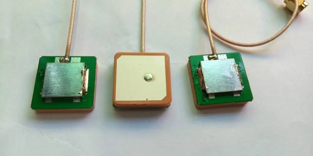
What are OEM Circuit Boards?

Rogers RO4835T PCB

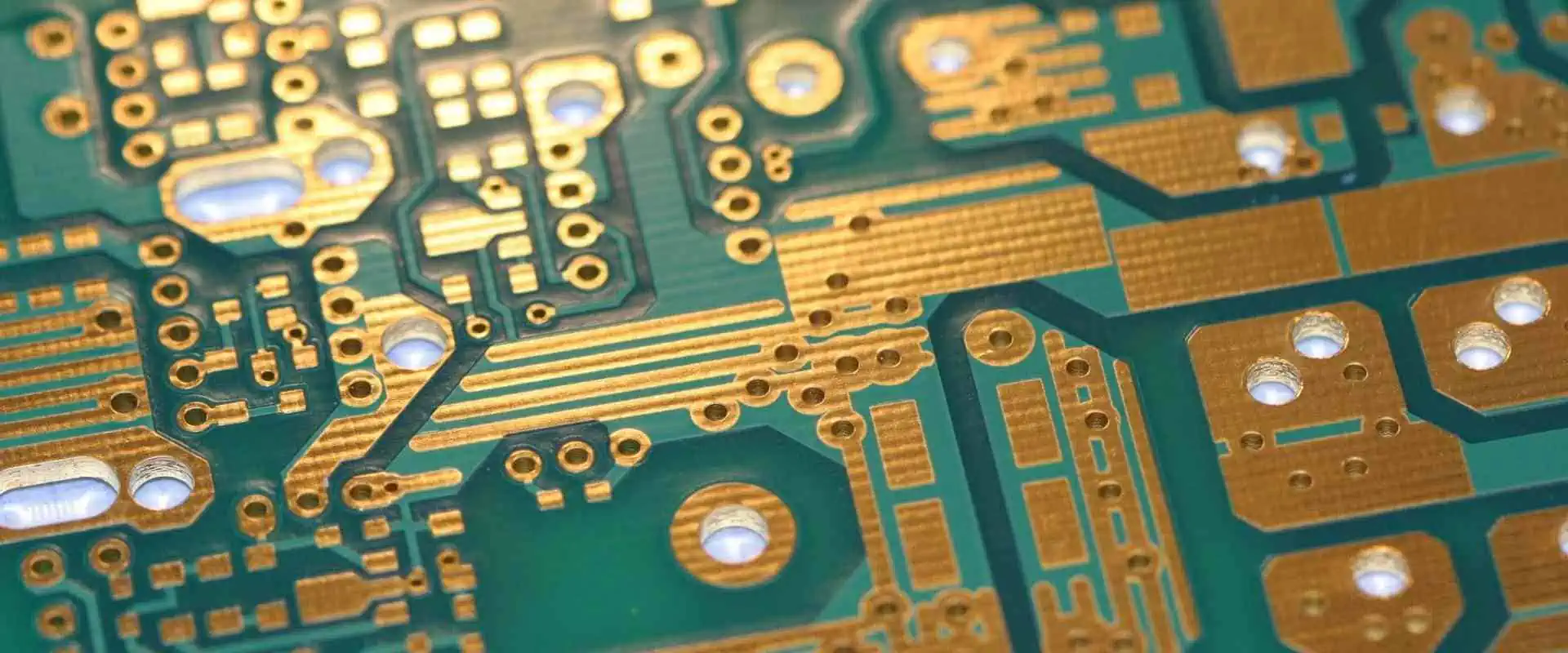
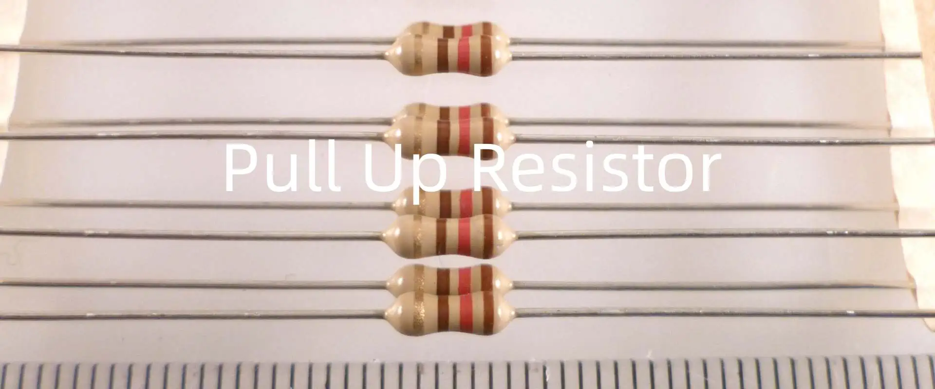
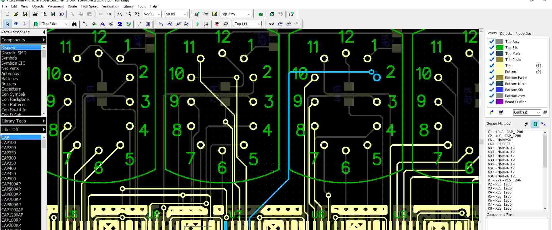
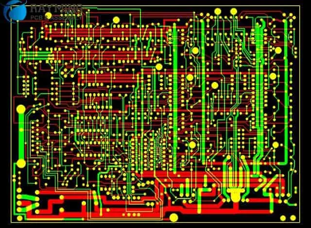
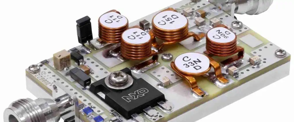
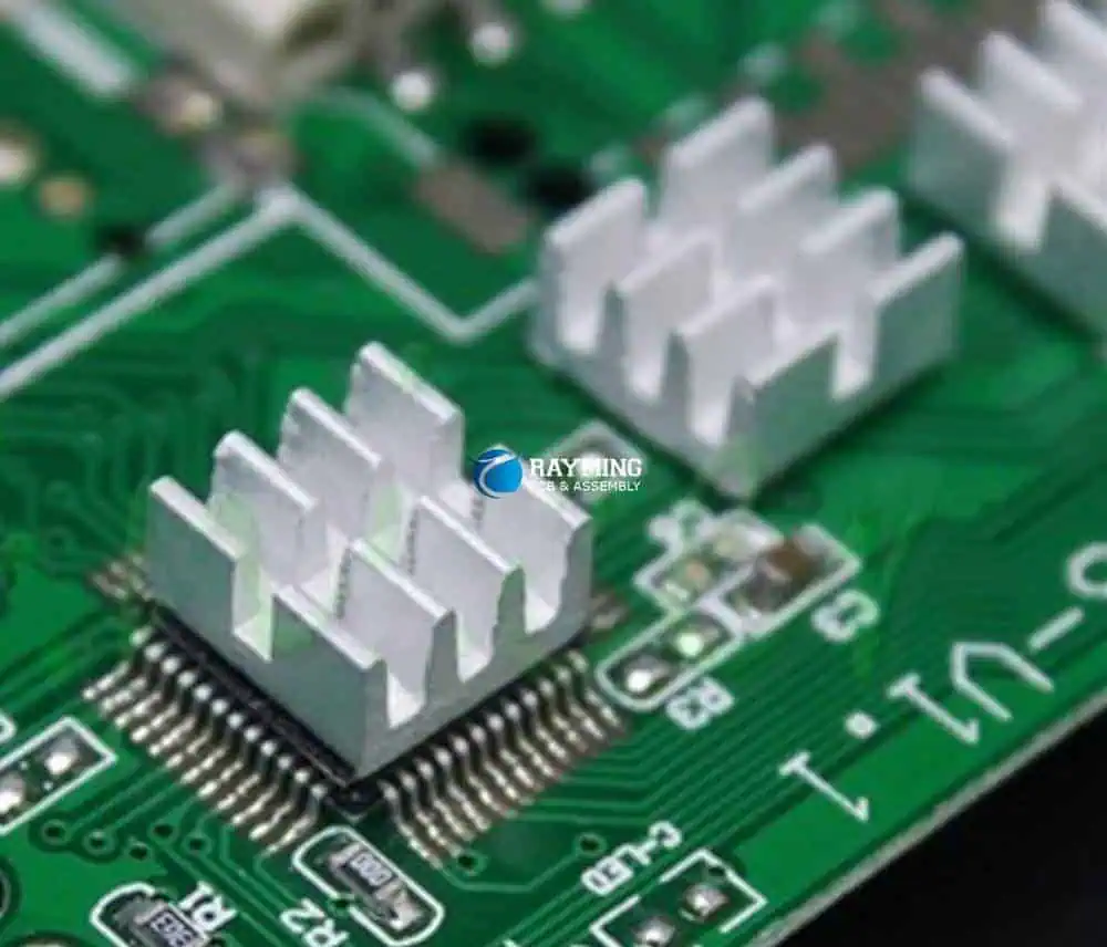
The OEM circuit boards are electronic assemblies which link components electrically using copper conductors. Electronic components are mechanically supported by circuit boards, allowing a device to be housed inside an enclosure. The manufacturing procedure, packaging of the integrated circuit, as well as they are bare printed circuit board structure must all be taken into consideration while creating the circuit board.

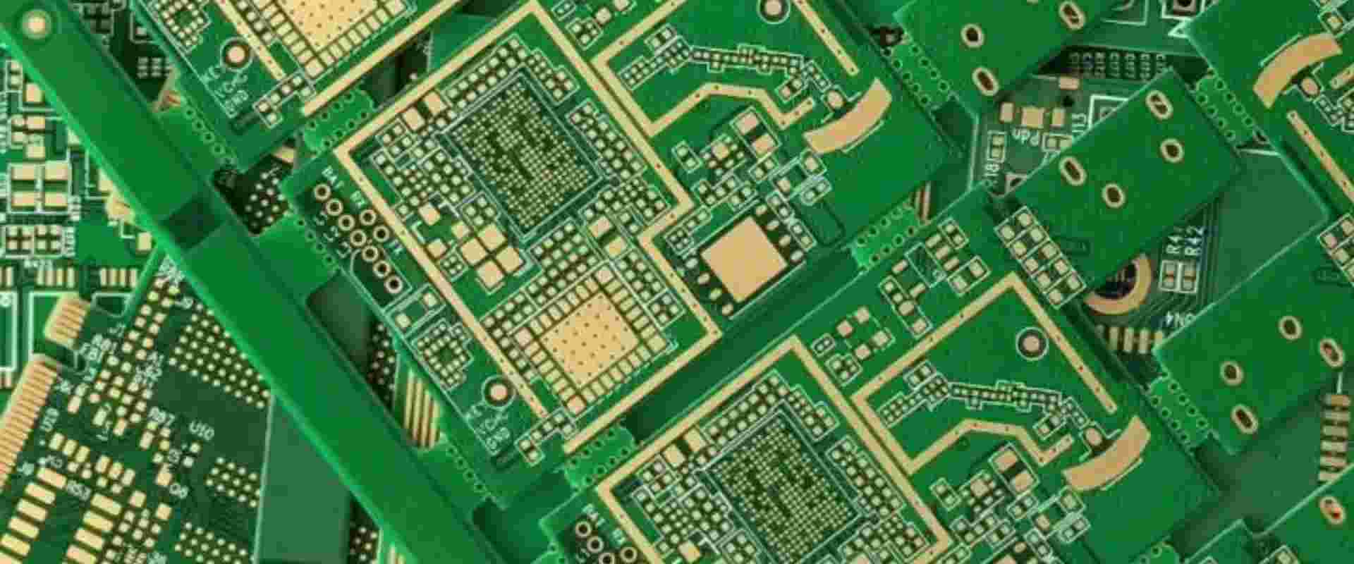
On the OEM circuit boards, conductive elements like pads, copper traces, as well as conductive planes are present. The insulating material gets laminated between conductor layers to form this mechanical structure. In order to offer an electronic component legend, the entire structure gets plated, covered in a solder mask (non-conductive), and then printed with silkscreen material.

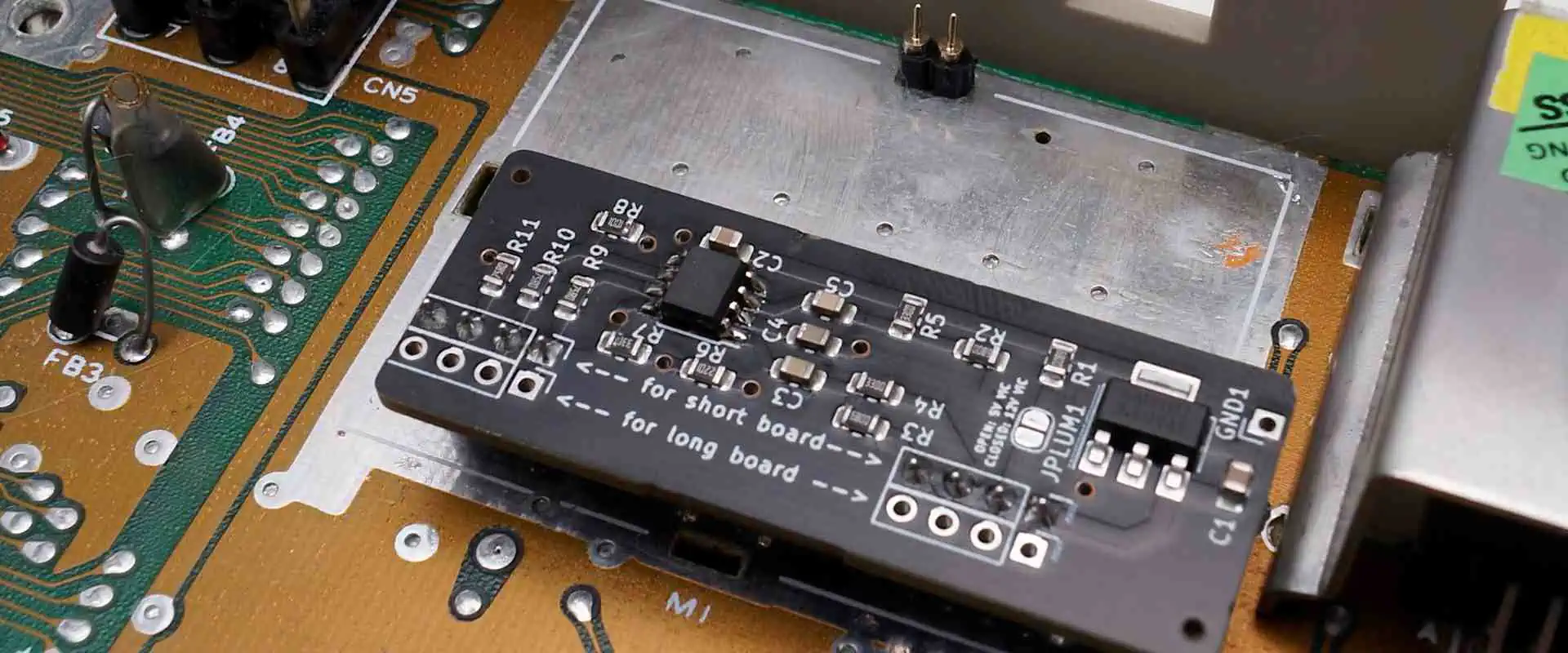
This bare board gets transported to the PCB assembly once these fabrication stages are finished so that components could be soldered onto the circuit board and then the PCBA could be tested.

Inside this electronics industry, PCB design has developed into a distinct vertical. PCBs are crucial because they offer sturdy support to keep components in place, electrical connections between components, and a small packaging that may be included into the end product. The ideal software will assist in taking a design right from the concept step then all through to the manufacturing. Even the simplest circuit board requires careful design utilizing special software programs.

We’ll delve into the definition of a PCB in this post, as well as some key ideas to keep in mind when designing your circuit boards.

Types of OEM Circuit Boards

FULL PCB MANUFACTURING Quote

Single-sided OEM Circuit Boards: Only one surface of this board is used to install components. Usually, the solder mask is applied on the totally copper (ground) surface.

Double-sided OEM Circuit Boards

On the two surfaces of this sort of circuit boards are installed components. The surfaces will have traces which carry signals in-between components since every surface is specified as the signal layer present in  PCB stack-up.

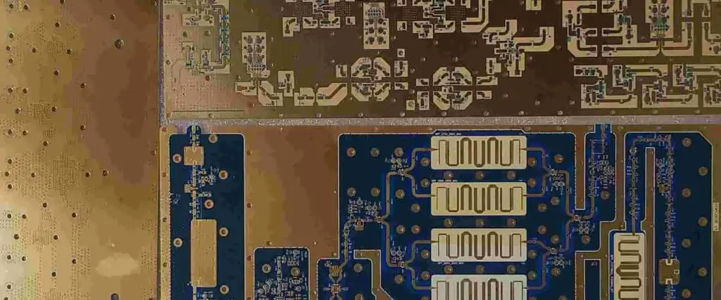
Multi-layer OEM Circuit Boards

The inside layers of these boards may be a conductive plane layer or conductors that transfer electrical impulses between components. PCBs with many layers can have either one or two sides.

Rigid OEM Circuit Boards

The boards are created and put together on stiff laminates like FR4-grade fiberglass laminates impregnated with epoxy resin. There are other varieties of stiff laminate materials that offer distinct material qualities for usage in specific specialized applications.

Rigid-Flex OEM Circuit Boards

In the PCB assembly, rigid-flex circuit boards join at least two rigid parts together using the flex polyimide ribbon. When this design needs to incorporate a moveable component, like a bending or folding enclosure, the rigid-flex circuit board may be used.

Flexible OEM Circuit Boards

Highly flexible PCBs are mainly composed of different flex polyimide ribbons and do not contain any stiff components. In the same way that rigid-flex and rigid circuit boards could have some components mounted as well as soldered on them, so can these boards.

Metal-Core OEM Circuit Boards

To provide far better rigidity as well as heat dissipation over traditional rigid OEM circuit boards, these boards incorporate one metal slab inside the core layer, often aluminum. There are some design considerations to make to guarantee solvability because the manufacturing process for metal-core rigid PCB designs differs significantly from the manufacturing process for ordinary rigid PCB designs. High-power lighting as well as several industrial applications frequently use these boards.

Ceramic OEM Circuit Boards

These less common boards are employed in applications requiring a thermal conductivity that is extremely high so that the circuit board can effectively dissipate significant quantities of heat off from the components.

Material for OEM Circuit Boards

A PCB’s base can be constructed from a variety of materials. The requirement is that the substance must be durable, insulating, and heat resistant.

The usual material used in manufacturing the OEM circuit boards include the following.

  • Ceramic
  • Copper coated with resin
  • Non-woven epoxy and glass
  • Woven epoxy and glass
  • Epoxy and cotton paper with or without phenolic

Applications of OEM Circuit Boards

Circuit boards are created by OEMs to satisfy specifications. These OEM circuit boards are widely used in a variety of applications, including:

Medical equipment

OEM circuit boards are being used by the healthcare industry in increasing quantities as technology develops and new capabilities are revealed. Devices utilized for diagnosis, monitoring, treatment, as well as other purposes often contain PCBs.

Boards for implants as well as numerous other uses, including monitoring for ERs, must likewise be relatively compact. As a result, a lot of PCBs for medical devices use HDI (high-density interconnect). As a result, a lot of PCBs for medical devices use HDI (high-density interconnect).  

Consumer Electronics

PCBs are necessary for the operation of computers, smartphones, and numerous other consumer goods that consumers use every day. PCBs are becoming a greater part of human’s everyday lives as we incorporate electronics into more products.

Small PCBs having a lot of connections are needed for the increasingly compact laptops and smartphones that are being produced by manufacturers. To bring the prices of the finished product low, PCBs used in consumer electronics must also be relatively inexpensive.

Automotive

Automobiles are using an increasing amount of different electronic components, according to automotive makers. OEM circuit boards once were mainly used for items like headlight switches and windshield wipers, but nowadays they allow many sophisticated functions that ensure easier and safer driving.

Telecommunications

A crucial component of the communications sector is the OEM circuit boards. Both the infrastructure which supports consumer electronics like cellphones and the devices themselves depend on them.

Types of Assembly Processes for OEM Circuit Boards

Through-Hole Mounting

The assembly worker inserts component leads in holes drilled to a bare OEM circuit board during the thru-hole installation procedure. The technology was first applied to PCBs.

Applications requiring high reliability use through-hole technology because it produces a much stronger connection compared to the surface mount technology. This is due to the fact that, unlike for surface mounting, these leads are completely embedded in the board rather than being connected with solder. The testing and development of applications which require manual component modifications can also benefit from the use of through-hole technology.

Surface Mounting

For surface mounting procedure, solder is used to attach components directly onto the circuit board surface. This technique was created during the 1960s and started to gain popularity during the 1980s.

It is currently the most popular component mounting technique. Instead of using through-hole components for connecting the different layers of a PCB, surface mount pcbs use tiny components known as vias.

The assembler can attach components on the board’s sides by making use of surface mounting. Additionally, because the surface mounted component could be smaller, more pieces can fit onto one single board. Because of the cost savings, electronic devices have been able to become smaller throughout time. In addition to being quicker and less labor-intensive compared to thru-hole mounting, surface mounting also has the advantage of being less expensive.

Why Choose OEMs for Your Circuit Board Manufacturing

Quality is guaranteed

OEM circuit boards with a quality guarantee are supremely precise and of the highest caliber. You can be certain that you will receive the same boards whenever you place an order with an OEM. OEMs create precise goods by working from the original component’s design template and blueprint.

They are aware of the materials to utilize at each stage of these components manufacturing, so you do not have to define the materials utilized. You’ll obtain the precise product you want, whether you work in the health, medical, or robotics sectors, you are sure to get the product you seek

Value

The value of the circuit board is what keeps your clients and draws in new ones. Keeping generic spare parts on hand could lower the price of your goods.

Affordable Prices

Dealing with the OEMs gives your company access to reasonable product costs. You can take advantage of proportionate cost savings because these manufacturers will develop bulk goods to serve the supply business.

Durability

100% durability is guaranteed for products purchased from the OEMs. Because it was created with accuracy, you do not need worrying about the quality of these materials as well as the product’s durability in demanding circumstances. Manufacturers cannot compromise component quality since they are aware of how important it is to consumers.

Conclusion

An OEM partnership can help a manufacturer as well as a reseller save money. Building manufacturing facilities and managing OEM production internally are not requirements for businesses. They merely incorporate the OEM components into the system and market their products under their brand name.

What You Should Know About Overmolding Circuit Boards?

Overmolding Circuit Boards

Most PCBAs come with a strong and protective barrier because they might occasionally be sensitive into environmental conditions. The injection mold procedure is used in this situation.

It is an effective approach to safeguard PCBAs and maintain visual appeal. We will now be able to see overmolding circuit boards clearly.

What Does a PCB Offer?

PCBs are little parts that make it possible for various forms of some modern technology so as to be able to function. In the past, connecting its wires from one onto the next was a laborious process for both production and maintenance. The idea of the printing of circuits on the top of your board resulted from this.

A basic conductive sheet serves as the basis for the entire procedure. With two layers of insulation provides support for conductive pieces.

A basic conductive sheet serves as the basis for the entire procedure. In most instances, a dual insulation layer provides support for a conductive element. Drilling is done on the sheets to make the registration holes required for accurate alignment. To make sure everything works in the right location for the CAD designs, then you can employ in-depth 3D models.

To be able to etch copper, the alkaline solution is employed, which aids in creating the proper tracing outline. It functions because UV lamps place the mask present on its copper layer, a process that may also be done in bulk. Utilize the optical testing device to examine the quality of copper traces for the short circuits as well as other types of damage. The solder mask coating’s distinctive greenish color provides insulation and protection.

Additionally, a silkscreen can print logos, markings, or symbols right onto the PCB.

How Does Overmolding Circuit Boards work?

The word “overmolding” describes a procedure that arranges and shields the component using injection or insert molding.

The first method is to put the PCBA assembly in place and then directly inject the overmold over it. This approach typically entails more alternatives for simplified look creation, color and logo customization, and the overall overmold design.

This second method of overmold injection involves providing a stronger barrier to serve the PCBA. It must be enclosed with a cap known as Lexan encapsulation in order to accomplish this. The design of the cap also enables it to accommodate the PCB as well as guarantee that it features a unique protective shell to protect vulnerable components.

The next stage after creating the cap is overmolding utilizing that very same options available for the process of instantaneous overmolding.

What are the Advantages of Overmolding Circuit Boards?

Nevertheless, while adding an additional degree of security, you must take the cost into account. Therefore, the question is: Is the investment worth it? A PCB component whose firmness is increased through overmolding circuit boards will perform better as well as be more resilient than one whose firmness is not increased.

Strength By having stronger flexural strength, high-traffic areas such as cable exits may take more tear and wear while still performing as intended.

Toughness

Overmolding provides wall protection for components. You will discover that because of this, extreme environmental factors including high temperatures, abrasions, impacts, water, as well as other types of external forces wonโ€™t bring any damage to them.

Maximum Security

Even severe external forces are protected by an additional shielding layer provided by overmolding. It serves as a direct protection component for your PCB.

Perfect Performance

The strain relief and pull strength capabilities of Circuit boards are improved by overmolding.

Enhanced Defense

Overmolding circuit boards aids in protecting components from corrosive substances like oil and saltwater.

Aesthetic appeal

Here, the truth is, aesthetically pleasing products typically sell better. O PCBs with overmolding circuit boards typically have better aesthetics and are simpler to integrate and maintain.

Customizing overmolds

There are various advantages to customizing Circuit boards using an overmold, including:

  • It supports the quality printing of business logos, names, as well as other types of branded messaging
  • Provides diverse angles for the exit point, including a straight angle, which is occasionally required to meet the objectives of a project.
  • It gives various locations that enable the integration of attached components such as a flange.
  • It permits the utilization of various overmolding materials, such as PVCs or thermoplastics.

Looking Closely at the Overmolding Circuit Boards Process

FULL PCB MANUFACTURING Quote

The procedure can be relatively straightforward or quite difficult. The decision about the machine as well as the material is crucial.

What Molding Equipment Should I Use?

The overmolding cable process is propelled by injection molding equipment. They can exert strong or low pressure to move any form of molten objects which has to do with the mold type needed.

The force necessary to suspend the molten resin inside the mold is referred to as tonnage when choosing your molding machine. More is required for larger molds. The method depends on using the right injection molding equipment.

Choosing the Best Materials for Overmolding Circuit Boards

One can employ a virtually infinite variety of materials to get a variety of results. One might result in the ideal rigidity, whilst another might produce more flexibility. However, everything is dependent on the requirements of a specific project.

However, TPU and PVC are two popular overmold materials (thermoplastic polyurethane). The latter is popular primarily due to its cost-effective qualities and is excellent for increasing strength and moisture-proofing.

Final injection molding

Following the selection of the material, the molding machine’s hopper will need to be filled, and its injection screw will then pump the material in the mold. This procedure will heat all materials in the barrel and press them in the tool-made mold. This will keep building pressure until a point whereby solidification is possible.

Conclusion

Having the right education as well as skill set is beneficial when dealing with physically delicate components like overmolding circuit boards. Failing to do this will result in subpar goods or possibly a molding machine malfunction. Contact us for your top PCB services, and a member of our staff with extensive experience will respond.

What are PCB Pins and How Do They Work?

pcb pin socket

The PCB pins can legitimately be referred to as the foundation of every PCB design. Similar to the way PCBs do, pins function like the interconnect system as well as various plug-in applications. The circuit board design does indeed have a significant amount of functionality thanks to hooks.

Circuit board pins can be pushed in to circuit, swaged, and, for most circumstances, soldered it to Circuit board in order to attach them to it. A necessary conductive channel for the electrical circuit is provided by PCB pins. As the mechanical interface, it gives an assembly module strength.

Types of PCB Pins

Header pins

In order to connect two components and perhaps a circuit board electrically, PCB header pins is frequently employed. Although there are numerous different kinds of PCB header pins, they are typically male connectors arranged inside a row and spaced apart by a set distance and range.

PCB Pin Socket

Such components that are difficult to mount on conventional connectors or circuit boards are frequently mounted using the PCB pin socket. The PCB pin socket is typically used on the Circuit board to select such features having single contact points. The ranges as well as dimensions of PCB pin sockets make it simpler for consumers to select one or more of their options based on their needs.

During recent years, press-fit pins have developed, making it simpler for engineers and designers to use the press-fit and solderless connectors. The PCB pins remain simple to utilize and produce the process of production less costly as well as being more accessible in contrast to the conventional methods. The engineer will find it much easier to debug a circuit in this situation.

The components installed on the Circuit board are mechanically supported by PCB alignment as well as PCB guide pins. On the other hand, PCB solder pins is among the most often utilized PCB pins when such connectors are attached to the circuit board top. Their typical uses are in the creation of circuit boards and prototypes.

PCB Jumper pins

Jumper pins on PCBs are frequently utilized to provide a path of conduction over a bypass component of an electrical circuit that is open or closed. They are necessary because the bypass connection must be made for the electronic components utilized in PCB board by the designer.

The PCB terminal pins were made to meet the expanding needs of the electronics sector. The PCB’s terminal pins offer separate, high-current connections. The designer can create multiple installation schemes to serve the designs thanks to the varied sorts and patterns of the PCB pins.

Engineers now find it much simpler to operate on prototypes or finished PCB designs because of PCB pin advances and enhancements. Many additional intricate patterns that would have seemed impossible to carry out using conventional techniques have now been made viable thanks to these breakthroughs.

How Does a PCB Connector Work?

FULL PCB MANUFACTURING Quote

The PCB connector is usually located on the circuit board and are often used in transferring power or signals from one Circuit board to another, as well as from some other source inside the unit, from or to the PCB. Since the Circuit boards are not permanently connected to one another and could be put together later during a process of production, connectors offer a simple way to design.

What are the Common PCB connector types?

PCB board connections are used in a wide variety of devices. The design therefore must be appropriate for the kind, size, as well as function. This makes a variety of PCB connector options accessible.

Wire-to-board Connectors

A cable is connected to a circuit board using this sort of PCB connection. The tool facilitates connections within circuits.

Male Pin headers and PCB connectors

These are essentially a series of pins having varied spacings, also referred to as the pin headers. There may be 0.197, 0.2, or 0.1 inches between each gap.

Board to Board Connectors

Manufacturers can link PCBs without the need for a cable thanks to the board-to-board connectors. The signal connection present between two Circuit boards is possible thanks to this connector. It could be a long-lasting bond with a connection that has to be “fit and forgotten.” The device uses receptacles and pins to link two PCBs.

Female PCB Connectors: These are also known as header receptacles or sockets. It firmly encloses its male connector, allowing the signal (data or power) to pass through.

Backplane connectors

This is a specific kind of PCB connection which can attach to different PCBs. It lowers signal rise and boosts data rates. Another PCB can be connected to a backplane connector, which is a form of support system. It also functions as the plane for users to interconnect daughterboards, which are additional system components.

USB PCB connector

Today, this is regarded as the most popular kind of PCB connector. It is hardly surprising because the USB port is used in many of the gadgets we use. Tablets, keyboards, computer mice, digital cameras, smartphones, and other devices, are very good examples.

How Can PCB Connector Be Tested?

It can be difficult to prototype and test circuits, so you won’t want to solder on the previously mentioned permanent connectors. It then becomes crucial to test and prototype connectors to serve as an option in such circumstances. With such a method, you may change things as you go without having to resolder any PCB components.

The following connector types are included.

Banana connectors

The โ€œConnectorsโ€ are machines that link several pieces of equipment. A power connection is made when the male jack is plugged into a female banana socket.

Alligator clips

This type of connector proves ideal for circuit experimentation with a variety of connections, while test running the circuit.

However, because they are intended to be utilized only temporarily, you must not rely on reliability of these connectors. As a result, it is frequent to find oneself maybe fumbling with its slick grips and creating inadvertent short-circuits, most especially if you manage to contact the nearby metal.

IC clips

This comes as an elegant connection that can be used to attach to the pins of the IC without the danger of touching its adjacent pins. It is ideal for troubleshooting requirements due to the characteristic.

Conclusion

The PCB pin socket is typically used on the Circuit board to select such features having single contact points. The ranges as well as dimensions of PCB pin sockets make it simpler for consumers to select one or more of their options based on their needs.

Functions, Benefits, and Limitations of Pull Up Resistors

Pull up resistor

Any digital electrical circuit will mostly contain pull-up as well as pull-down resistors if you look into it. In the absence of an input condition, they are employed to properly bias digital gates’ inputs to prevent them from randomly floating around.

Pull-up as well as pull-down resistors use output and input signals for microcontrollers in any embedded system like an Arduino to communicate with different hardware devices.

What Does a Pull Up Resistor Mean?

Electronic circuits utilize pull up resistors to maintain a signal’s known state. To ensure that the voltage across ground and the Vcc is effectively controlled whenever the switch is turned on just like the pull-down type), it is typically used in conjunction with switches and transistors.

It is known as a fixed resistor linked between an input pin as well as the supply voltage; it isn’t an unique kind of resistor. You frequently encounter this pull up resistor within digital circuits since it is so widespread. It merely consists of a resistor linked from such an input to VDD, which is the circuit’s positive supply.

Pull up resistors can be described as resistors that are employed in different logic circuits in order to guarantee a consistent logical level present at the pin. Recall that there are three main logic states in the digital logic circuit: high, low, and floating (which is also called high impedance). When this pin isn’t pulled onto a low or high logic level however it is instead left “floating,” it enters its high-impedance condition.

A micro controller’s input pin that isn’t connected serves as a good example of this. The microcontroller may erroneously interpret the value of the input as either the logical high as well as logical low because it is either a high or the low logic state. The microcontroller’s conundrum is resolved with pull up resistors, which raise the value onto the high state.

How Does the Pull up Resistor Work?

Zero Ohm Resistor

Between the supply voltage as well as the input pin, the resistor is attached. Whenever its mechanical switch seems to be off, the input voltage gets raised to the input voltage level. Additionally, whenever its mechanical switch gets turned ON, the input power is sent straight to ground. To guarantee the level of voltage, the switch is linked with the pull up resistor. The switch regulates the circuit’s input state.

The switch of the power electronics is also utilized inside the circuit in place of the mechanical switch. Since the pin canโ€™t be connected to the supply or ground directly, this pull up resistors are also necessary to prevent short circuits. Other circuit components may be damaged or shorted out if this pull up resistor isn’t connected.

To create a second loop over all the crucial parts and guarantee that this voltage can be well-defined even while this switch has become open, the pull up resistor can be utilized. When there is no input signal, it is utilized to make sure that the wire pulled into a higher logical level. It is a standard type of resistor.

They are straightforward fixed-value resistors attached between this voltage supply as well as the proper pin that, in the absence of a driving signal, specifies the output or input voltage.

This gate input’s voltage is dragged up to that input voltage’s level when this switch is open. This gate’s input voltage passes directly into the ground whenever this switch has been closed. Whenever there’s a low default state of impedance and want to pull this signal into “high,” you must employ the pull up resistor.

What are the Use Cases for Pull Up Resistors?

FULL PCB MANUFACTURING Quote

When connecting the switch and perhaps other input into this microcontroller as well as other several digital gates, the pull up resistors are frequently employed. Lower external components will be required because most microcontrollers feature built-in pull-up programmable resistors.

These microcontrollers can be connected directly to switches. Although certain microcontroller families featuring both pull-up as well as pull-down resistors present, the pull up resistor is typically utilized more frequently than the pull-down resistors.

They are frequently used to deliver a regulated current flow to a resistive sensor before the voltage signal of the sensor output is converted from analog into digital. The pull up resistor is also utilized in the I2C protocol bus, where they allow a single pin to function as either an input or an output. The pin floats in an extremely high-impedance condition when it is not linked to a bus.

  • Pull-down resistors have become less common compared to the pull up resistors in use. The usage of the pull up resistors is described in the list below.
  • The pull up resistor is utilized as interface components between switches and digital circuits.
  • Also, it is utilized in I2C protocol buses in enabling the signal pins to serve as the output or input
  • For the resistive sensors, you can utilize them in controlling the flow of current before the conversion from analog into digital

Choosing the Value for the Pull up resistor

The price shouldn’t be excessive

The input voltage decreases as its pull-up value increases. The voltage must be sufficiently high for this chip to recognize it as the HIGH, as well as logical 1, inputs. For instance, the CD4017 having a 10V power supply needs at least 7V mostly on input to be recognized as HIGH.

It also can’t be very little

The issue arises if, for instance, you select 100, as there is much current passing through it whenever you pressing of the button. The 9V power source gives you 9V across the 100, or 90 mA.

The resistor must be capable of withstanding 0.81W, which is a needless waste of electricity. Most resistors only have the ability to handle 0.25W at a time.

General Rule

Pick the pull up resistors having a value of resistance that is about 10 times lower than the pin’s input impedance (or internal resistance). Frequently, a 10 kฮฉ pull-up value will work. But keep reading if you wish to know how it operates.

Why Pull Up Resistors are Important?

Pull up and Pull-down Resistors

The pull up resistors are utilized in raising the digital pin’s default state to high or to its logic level, and the pull-down resistor performs the exact opposite, which makes the digital pin’s default pin to become low (at 0 volts).

But why do we need all those resistors whenever the logic pins may be connected directly into the voltage of the logic level or to the ground instead? While the pull-down resistor could successfully control the flow of current from the digital pins onto the ground, the pull up resistor allows controlled flow of current from the source of the supply voltage into the input pins. Pull-down as well as pull up resistors simultaneously hold this digital state in either high or low range.

Use pull-down or pull up resistors if you require a basic logic state but wish to change it in response to user input as well as external peripherals.

What are the Values of Pull Up Resistors?

There are two constraints on the pull-up (as well as pull-down) resistor’s appropriate value. Power dissipation is the primary consideration.

Whenever the switch gets closed, a significant amount of current will pass through this pull up resistor if the value of resistance is extremely too low, heating the component and consuming extra power. Whenever the consumption of low power is required, a powerful pull-up, like it has known, should be avoided. This pin voltage while the switch becomes open is the 2nd factor.

This input voltage may not be sufficient whenever it is an open switch if the value of the pull-up resistance becomes too high and input pin has a significant leakage current. Having relatively weak pull-up is the term for this situation. The input pin’s impedance, which is directly connected to the leakage current of the pin, determines the precise value of the resistance of the pull-up.

The Drawbacks of the Pull Up Resistor

These resistors’ inability to be useful with anything greater than a button is one of their drawbacks. This is due to the resistor’s inability to push current across all of the additional buttons. Additionally, the resistance cannot alter for the other directions because it only permits one current only to flow in one direction. Another circuit, like a “Schmitt trigger,” which has a greater impact than a single push button, can be substituted for it.

We can’t give the circuit enough time to flip from a high to a low when pressing the buttons quickly. As a result, the resistance does not release any energy, and the circuit does not experience any current flow. This is known as “Hold-off.”

Light switches cannot be used with pull up resistors because current just wouldn’t pass through them. As a result, it stops light from turning on. Also,  e avoid using pull up resistors when a switch is off for an extended period of time. Since it won’t let the electricity flow, it must be switched off for longer period of time than usual, which will save money.

Conclusion

When connecting a switch as well as other input to a microcontroller and other types of digital gates, the pull up resistor is frequently employed. There are typically programmable built-in pull up resistors built into microcontrollers, which reduces the requirement for external components.

Diptrace Vs FreePCB: Differences in Features and Functions

Diptrace Vs FreePCB

It can be difficult and frustrating to get a good free PCB design software tool with all the design software available online. We will be evaluating two PCB design software tools which are Diptrace vs FreePCB. In this article, we will be making a comparison between Diptrace Vs FreePCB. These tools are great design tools to help you achieve a good PCB design.

The FreePCB currently runs on Windows only. Also, the source code of FreePCB is copyrighted. If you need a software application to design a 2-4 layer board DipTrace is an ideal option for you.  DipTrace is very intuitive and easy to learn with a low learning curve. The comparison between these PCB software free tools will be in terms of compatibility, features offered, supported platforms, and availability.

What is DipTrace PCB Design Software?

diptrace

DipTrace is a CAD software application specially designed for the creation of schematic diagrams. Also, it is an ideal software application for designing printed circuit boards. DipTrace features a multilingual interface, it is available in English and 21 other languages. This CAD software comprises 4 modules which are pattern editor, schematic capture editor, PCB layout editor, and component editor.

DipTrace features a drag-and-drop approach ideal for 4K monitors. Also, it has simple design rule checking and real-time 3D visualization. Furthermore, this CAD or EAD software has an active community of users and as well features good training materials and tutorial. Users can check out its active YouTube channel.

 DipTrace is well known for its ease of use while still maintaining functionality. This software has a normal license fee. With advanced features like schematic capture level hierarchy, Gerber output, autorouter, and real-time DRC, this software helps in achieving an efficient design. The user-friendly software is ideal for both beginners and professionals. Without even learning how to use this software, you can get started.

This schematic and PCB designing software allows you to create 3D designs and multi-layer boards. Also, this software application includes features like a component editor. The component editor allows you to define multi-part components through electrical or physical parameters.

DipTrace is one of the simplest programs for your PCB design. This PCB design software application is very affordable and is ideal for hobbyists. However, it is less ideal for very complex schematics.

If you need a software application to design a 2-4 layer board DipTrace is an ideal option for you.  DipTrace is very intuitive and easy to learn with a low learning curve. This software comes with a free version which is fine for simple projects.

Design Tools in DipTrace

FULL PCB MANUFACTURING Quote

Schematic Capture

The schematic capture tool enables you to link pins with no need of wires. Also, this tool can help you convert your schematics to circuit board. With the multi-level hierarchical and multi-sheet design, engineers can visually connect pins. Schematic supports the export and import of various CAD/EDA tools.

Library creation

The library creator is in two parts. These are pattern editor and component editor. The pattern editor allows users to create pattern with various dimensions, holes, shapes, and pads. Also, this editor comprises rectangle, square, matrix, Zig-Zag, and circle templates. Users can create multiple or single components and manage libraries with the help of the component editor. Also, you can design non-custom patterns . The DXF import enables users to easily create complex layouts. Users can build complex components by integrating various features such as editing, bulk pins-naming, and pad numbering.

Component editor

The component editor is an important tool in DipTrace. This tool creates multi-part components and manages component libraries. Also, users can use the component editor to choose a dimension setup and template. DipTrace defines the parameters of electrical pin parameters and fixes patterns with 3D models.  

This software Diptrace can import libraries from different EDA formats. Also, you can use it to design non-standard patterns and as well create complex layouts. To achieve this, select the template and enter crucial parameters.

Pattern editor

The pattern editor helps users in creating patterns of various shapes and dimensions. Also, it can draw sizes, lines, and pads. With the pattern editor, engineers can draw rectangles and zig-zag templates. Choosing the right pattern helps you enter some relevant parameters.

3D modeling

3D modeling displays your PCB components in the 3D view. This enables the PCB to rotate at axes. You can as well zoom in and out, makes changes to the boardโ€™s color, solder mask, copper area, and silkscreen. 3D modeling works on all stages of the design, this is one good advantage of the board. The main purpose of this tool is to allow users to view the PCB from any angle or any side. With this, you can check the maximum errors.

PCB Layout

layout
layout

 The PCB layout tool that is ideal for careful placement, shape base auto-router, and creative projects. Sometimes, your PCB layout may fail during PCB manufacturing. This can impact the functionality of your final circuit board in the long run. There are a wide range of high-level PCB layout tool that features manual routing for differential and high-speed signals.

With the verification feature, users can easily check the accuracy of the complex project by integrating high-speed signals. The PCB layout comprises another useful feature known as real-time DRC. The design rule check (DRC) helps users to correct their errors and as well improve the quality of their PCB  project.  

Placement tool

 The placement tool has drag-and-drop features, which enables organizations to include various components by features and some custom attributes. This helps in specifying the final PCB. Also, the placement tool provides a wide range of features like data export/import, interactive visuals, 3D modeling, and more. Furthermore, this tool allows administrators to have a 3D view of the final printed circuit board. Also, they can rotate and zoom in or out photos on the axis.  

Features of DipTrace

  • It has High-speed shape-based auto-router
  • Comes with verifications with real-time DRC
  • Has real-time 3D PCB preview
  • Enables engineers to rotate, zoom in and out the printed circuit board whenever they want.
  • It shows models of the printed board and the installed components.
  • Also, it allows users to make changes to colors as well as the background.
  • Exports PCB to Step 3D file format
  • ODB++ and Gerber (including Gerber X2) manufacturing outputs
  • Easy to learn and friendly User Interface
  • Shape-based autorouter
  • Smart manual routing tools
  • Multi-sheet and hierarchical schematics
  • Wide import/export capabilities

The Diptrace has a free version which  is available for everyone. Also, this free version has all the functionality the complete package has. However, the only limitation of the free version is that it is limited to 300 pins. Users can still create a four-layer board with power planes and ground planes using these features.

There are several features that helps in controlling the different functions such as checking ERC (electrical rule checks), component searching, and connectivity checking.

These features can exist in either of the states. This indicates the file can work well in PCB layout or as Gerber.

What is FreePCB?

This is an easy-to-use and effective PCB designer software. Free PCB is specially created for Microsoft Windows and it is capable of professional-quality work. Also, this software can design PCB with 1 to 16 copper layers.  For most of its functions, it integrates metric units (i.e. mils or mm).  Also, this PCB design software application is equipped with a wide range of tools such as footprint editor, footprint libraries, and footprint wizard. The footprint Editor helps to modify or create footprints, exports extended Gerber files (RS274X) , imports and exports PADS-PCB netlists.

Free PCB software has a user-friendly interface and a lot of impressive features. This software package doesnโ€™t include a circuit diagram software. Therefore, you will have to make use of other software to draw your circuit and design it. This might be a bit difficult for you to design a PCB if you are not really familiar with this PCB software. However, the Free PCB was specially designed to help designers achieve a great PCB design. Therefore, this software prepared a very useful user guide.

There are chapters on the PCB design in this user guide. Also, there is a tutorial which teaches users how to go through the process of designing a circuit board from a schematic. With this tutorial, you will get to know the main features of Free PCB.

Beginners will have to check the user guide ebook to get started. The user guide ebook will provide answers to all your questions. Also, this guide contains any details that you may need from the footprint editor, PCB start up, and keyboard shortcuts.

The FreePCB currently runs on Windows only. Also, the source code of FreePCB  is copyrighted.  However, it is released under the General Public License

Features of FreePCB

Features of FreePCB Include:

  • It has up to 16 copper layers
  • The size of the PCB Board is about  60 inches by 60 inches
  • Integrates metric units (i.e. mils or mm) or English for the majority of its functions.
  • The Footprint libraries strictly adhere to PCB Matrix and the IPC.
  • Has Copper fill areas
  • The Footprint Editor and footprint wizard helps to change or create footprints
  • It can export and import PADS-PCB netlists
  • Capable of exporting  Excellon drill files and  extended Gerber files (RS274X)
  • Comes with Design rule checker
  • Autosave

What is the Difference Between DipTrace Vs FreePCB?

DipTrace is well known for its ease of use while still maintaining functionality. This software has a normal license fee. With advanced features like schematic capture level hierarchy, Gerber output, autorouter, and real-time DRC, this software helps in achieving an efficient design. The user-friendly software is ideal for both beginners and professionals. Without even learning how to use this software, you can get started.

FreePCB software package doesnโ€™t include a circuit diagram software. Therefore, you will have to make use of other software to draw your circuit and design it. This might be a bit difficult for you to design a PCB if you are not really familiar with this PCB software. However, the Free PCB was specially designed to help designers achieve a great PCB design. Therefore, this software prepared a very useful user guide. Beginners will have to go through the user guide to get started.

This schematic and PCB designing software allows you to create 3D designs and multi-layer boards. Also, this software application includes features like a component editor. The component editor allows you to define multi-part components through electrical or physical parameters. DipTrace is one of the simplest programs for your PCB design. This PCB design software application is very affordable and is ideal for hobbyists. However, it is less ideal for very complex schematics.

Free PCB is specially created for Microsoft Windows and it is capable of professional-quality work. Also, this software can design PCB with 1 to 16 copper layers.  For most of its functions, it integrates metric units (i.e. mils or mm).  Also, this PCB design software application is equipped with a wide range of tools such as footprint editor, footprint libraries, and footprint wizard.

Conclusion

Hope you now know the differences between Diptrace vs freepcb. The process of laying out of traces on a printed circuit board is complex and as such requires much attention and carefulness. The advent of PCB layout software have made it much easier to handle this task, however, there are still some challenges being faced by designers.

The circuit is usually designed by an electronic engineer. Also, PCB design is a process that requires a specialized skill. Over time, a wide range of advanced PCB design software applications have been developed. PCB design requires the integration of several techniques and adherence to certain standards.

With the various types of software available for PCB designing, some applications donโ€™t offer what is required.  The first thing required in a PCB design is the schematic diagram of the PCB. After this, a layout needs to be created by using software. Also, you need to print the layout on the circuit board after the placement of components and application of solder.

How to Choose Your HDMI RF Modulator

rf modulator

Since outdated connectivity ports like analog video/audio connectors are no longer relevant, new generation Televisions, consoles, and monitors primarily offer a small number of connecting possibilities. The main connecting option in most media devices, including Xbox and Playstation, is HDMI. As a result, connecting older Televisions as well as monitors to such modern gadgets becomes a little challenging.

To connect conventional I/O ports as well as HDMI inputs in this situation, you will require an HDMI RF modulator. Since RF modulators really aren’t particularly common, you might now be aware of what to look for when purchasing one. Before purchasing an HDMI RF modulator, be sure to read the following crucial information.

What Does an HDMI RF Modulator Mean?

RF Amplifier Manufacturer

Devices having HDMI output can provide HDMI input to the RF modulator. This covers consoles, set-top boxes, and media players. It transforms the signal coming from these gadgets into a radio frequency, or RF. Then, this is sent over a wire, typically an A/V cable or coaxial cable. If you prefer to go wireless, these RF waves are also received by Televisions with antennas.

RF modulators with various input characteristics come in a variety of sizes, forms, and colors. However, since HDMI RF Modulator is what we are mostly discussing, HDMI is typically the input. Therefore, every modulator should have an HDMI connector that can accept input from contemporary devices including consoles, gaming computers, laptops, Blu-Ray Players and smartphones.

Modulation

RF Modulators operate by transforming HDMI signals into radio frequency, or RF. Direct conversion, however, may result in quality loss or stuttering in the audio and video. Interference is typically to blame for this. To avoid this, waves of higher frequency are added to or blended with HDMI signals. The “modulation” enters into action at this point, therefore the name.

In summary, it accepts a signal as the HDMI input, transforms it to a RF signal, then corrects the quality loss. The image/video then appears on your TV without experiencing any significant image quality reduction. Of course, the type of TV that you use with the modulator also has a significant impact on this.

Output

The RF Modulator would output the video or image to your preferred TV after a small amount of quality improvement has been made throughout the modulation process. A HDMI RF modulator typically has just one RF output. Coaxial cable is required to connect your gadget onto your TV. On some of these modulators, you may even discover a HDMI output. That will be useful if you wish to connect various Televisions or displays using just one source.

RF Modulator Buyer’s Guide

FULL PCB MANUFACTURING Quote

Sure, the market for RF modulator is complicated and loaded with confusion. Finding a decent alternative can be challenging and overwhelming for a first-time buyer, and the market’s saturation makes matters worse.

Quality of Video

When deciding whether to purchase the HDMI RF modulator, video quality stands as a key consideration. Therefore, it would be a good idea to regularly verify video output inside the designated region.

Everyone has preferred qualities whenever it regards quality. The majority of modulators now provide a video output of 1080p, which is generally sufficient with most people. However, if you want the best 4k experience, this can be pricey.

Accessories Included

You will also need connectors, cables, power adapters, as well as other items in addition to the HDMI RF modulator. You will be unable to install your device or make any connections without these mandatory peripherals. Many manufacturers of these modulators provide all essential peripherals in the box.

Because the HDMI RF modulator may cost a significant amount of money, you should ensure the box contains all the components you will want. It is perfect for speedier installs and spares you the hassle and additional money of purchasing extra components in the future. The mounting connection cables, brackets, as well as power adaptor utilized in powering the device are the three main accessories that serve the HDMI RF modulators that are most crucial.

Connectivity

Different connectivity RF modulators are available with various output and input supports. And from personal experience, it can be a great headache if you purchase something just to discover that it is incompatible with your device. Therefore, learning a little bit about the TV’s connectivity as well as the input options and ports it has is helpful.

Worth the Money

hdmi-pcb-connector

Like anything else, the HDMI RF modulators come in a wide range of costs. While some solutions cost less than $100, some exceed $500. Surprisingly, there is absolutely no correlation between the pricing and the modulator’s quality.

It generally depends on your specific problem, it is nevertheless a good idea to examine its feature list as well as determine whether it offers value for the money and whether the price is reasonable given the characteristics. It is wise to weigh the benefits of the more expensive features against those of the less expensive ones.

Application and Installation

Even if your chosen HDMI RF modulator meets all the aforementioned requirements, it is nevertheless not the ideal option if you cannot install it. You could have common issues like damaged wires, loose connections, unreachable devices, etc. if your installation is not done properly.

Therefore, before you purchase the unit, be sure to examine the device’s size and establish an installation plan. This should help you get a sense of the space that is available next to the Television or monitor so you can determine whether the gadget will fit there or not. You should also be aware of the device’s suitability for the connection. Check your power settings, onboard controls, as well as the capability of the remote control, if offered, for that.

Conclusion

Hope you now understand what the RF modulator is. We have also included a buyerโ€™s guide which will help you make the best decision. Devices having HDMI output can provide HDMI input to the RF modulator. This covers consoles, set-top boxes, and media players. It transforms the signal coming from these gadgets into a radio frequency, or RF.

Features and Benefits of SMD 0805

SMD 0805

There are different types of SMD packages. When we talk about SMD package types, we refer to the physical characteristics of surface mount devices. Surface mount devices are usually attached with the integration of the surface mount technology (SMT). Also, the surface mount technology involves the mounting of electronic components directly on the printed circuit boards (PCB) surface.

Surface mount technology supports the integration of automated equipment. Therefore, this makes it suitable for miniaturized components. Today, SMT is widely integrated for mounting SMD components like integrated circuits (ICs), resistors, capacitors, diodes, and transistors. In this article, we will be discussing the SMD 0805 and its features.  

What are SMD Package Sizes?

An SMD is an electronic component mounted on a PCB surface with the integration of SMT. This mounting method is a faster alternative to through hole technology (THT).  SMDs are available in a wide range of land patterns and package sizes. PCB manufacturers and engineers can make use of the ECAD to replace any obsolete SMD component.

The physical dimensions of SMD packages are used to describe them. Also, these packages have lettered or alphanumeric codes that describe them.  Also, Standards and packages need to conform to EIA specifications.

There are a wide range of SMD package types. SMD capacitors and SMD resistors feature rectangular packages. Each of these packages has numbered designation. Some of the most common SMD package types are 2920, 2512, 0603, and 0805. The SMD 0805 has become so popular in the electronics industry. Furthermore, this SMD package size is popular due to its ease of assembly, low price, and as well as its small land area. ย ย 

What is SMD 0805 Package Size?

SMD Fuse

The SMD 0805 package size is 2 X 1.3mm (length X width). This means 0.08 x 0.05 inches. One of the advantages of this SMD is that it is very easy to hand-solder. Also, the smallest SMT resistor is the 0805.

0805 is simply a numerical code that shows the specification of the size of SMD resistors. Also, this code defines the SMD package in terms of length and width. Therefore, SMD 0805 is an SMD package that is  0.08โ€ in length and 0.05โ€ in width. There are two different naming standards and sizing in the SMD package footprints. This simply specifies footprints for 0805 components in the imperial and metric units.

The SMD 0805 component is ideally the imperial version of a 0805 package footprint. Furthermore, the 0805 SMD metric package is a much better option compared to 0603. One of the benefits of SMD 0805  is that it fits the vero board. The 1206 doesnโ€™t fit the vero board since it has a very small size.

Features of SMD 0805

SMD 0805 is a low profile and small footprint package size with excellent illumination. This SMD package size is suitable for portable consumer electronics  due to its wide viewing angle. Also, this package size is easy to assemble and features a small land area.

It is a low-cost solution for compact and low power electronic designs. SMD 0805 is compatible with automatic placement equipment. This SMD package size is easy to hand solder due to its size.

One of the features of SMD 0805 is that it fits the vero board. The 1206 doesnโ€™t fit the vero board since it has a very small size.

There are two different naming standards and sizing in the SMD package footprints. This simply specifies footprints for 0805 components in the imperial and metric units.

More Facts about 0805 SMD

FULL PCB MANUFACTURING Quote

There are thousands of tiny components in electronic devices. These tiny components known as surface mount devices contribute to the functionality of electronic devices. Surface mount technology (SMT) is integrated when mounting these. Traditional components have wire guides. Therefore, surface mount devices are widely used among PCB manufacturers, engineers and designers .

Also, SMT mounts SMDs directly on the surface of PCBs. Since these devices are usually very small, a pick and place machine is used in picking and placing them on the bare circuit board. There are a wide variety of surface mount devices like resistors, capacitors, ICs, and diodes among others. These SMDs are available in several sizes.

Therefore, it is important to understand the dimensions, lengths, widths, and land patterns of these devices. ย Also, knowing the right size for your electronic circuits will help you greatly. The 0805 SMD package size is one of the commonest package size used among PCB manufacturers.

Note that the 0805 is simply a code that specifies the size of surface mount devices. The size of a surface mount device is as important as the component itself. Size determines a lot when mounting an SMD component on bare board. Also, it is one of the physical attributes of SMDs. The designations in SMD capacitors and resistors represent inch based measurements.

The physical dimensions of SMD packages are used to describe them. Also, these packages have lettered or alphanumeric codes that describe them. ย Also, Standards and packages need to conform to EIA specifications.

Frequently Asked Questions

How much power is an SMD 0805 resistor capable of handling?

The 0805 size pulse resistor is capable of handling over 100 watts at a single pulse and for the same duration. However, the width of the part of a standard thick film chip resistors feature laser trim. Also, the laser trim can reduce the effective width of the resistive element.

What is the voltage of SMD 0805 resistor?

SMD 0805 resistor has a voltage ranges between 60 to 70V. However, they can go higher than this with more specialized resistors.

Conclusion

0805 is simply a numerical code that shows the specification of the size of SMD resistors. Also, this code defines the SMD package in terms of length and width. Therefore, SMD 0805 is an SMD package that is  0.08โ€ in length and 0.05โ€ i width. There are two different naming standards and sizing in the SMD package footprints. This simply specifies footprints for 0805 components in the imperial and metric units.

Importance of SMD Heat Sink in Electronic Circuits

SMD heat sink

It is possible in electronics for your PCB to become quite warm as a result of power loss in some components. A component’s lifespan will be significantly decreased or it may fail right away whenever it reaches an excessive temperature that is above its safe operational range.

The whole PCBA will have to be discarded because its heat-production component is faulty. When it comes to controlling heat on your board, there are several factors to take into account. It all starts with figuring out how much power your design will dissipate during the schematic capture. Also, you might require the SMD heat sinks on some components in high power devices if you’re working within safe parameters. In the end, this might keep your components, the operator, and the product.

What is an SMD Heat Sink?

Heat Sink PCB

A great technique to effectively disperse heat from large power components is with the SMD heat sink. You’ll like to make sure the appropriate mechanical model and footprint are produced, that you possess the finest PCB design tools available to utilize it, and that the SMD heat sink come in a variety of sizes and forms.

Heat sinks move heat from the source into a location or element that is more readily dissipative as well as less prone to result in heat related aging problems using the concepts of thermal routing design. Similar to electrical routing, this thermal routing depends on the conductive materials, ample pour areas, plus vias to handle that heat flux moving from its generation points.

Whenever this circuit is operating, heat is produced by every electrical component in the circuit. Heat is produced by high-power electronics like lasers, LEDs, and power transistors. Due to their poor heat dissipation abilities, some components cannot dissipate heat.

This device may completely fail or fail prematurely as a result of the building up of heat in this component. Therefore, boards for heat sink are the ideal solution to solve these issues. Due to their cooling capabilities, the circuit boards play a useful role in the majority of applications. Due to the many advantages the SMD heat sink provides, PCB makers incorporate one in their products.

How to Mount an SMD Heat Sink

FULL PCB MANUFACTURING Quote

We don’t always mean to refer to the component which solders onto the PCB’s surface layer whenever we say “SMD heat sink.”

To effectively dissipate heat away from a component, these devices could be placed directly onto the component package. Also, t hey could be utilized as the bridge to transfer heat into such an enclosure or affixed to the underside of the PCB.

Thermal pads or thermal compounds like grease are used when mounting the SMD heat sink. Instead of using the SMD heat sink, a high-power component may feature a thermal pad or thermal tab that you connect to a PCB pad (to a specific GND net). However, if necessary, you may still attach SMD heat sinks to any of these parts; this is typical in sections of power delivery that utilize MOSFETs arrays; one huge heat sink could be soldered through many components in order to help in dissipating more heat.

Heat is a bigger issue since smaller PCBs must accommodate more computing power in the smaller packaging. These compact boards might not have enough room for the fans, sizable heat sinks, as well as component spacing to stop heat from spreading across the board. This same temperature of your main heat-generating component will frequently rise to significantly higher values when you install a board having excessive heat dissipation within any closed enclosure.

Vents undoubtedly aid with airflow exhaustion and temperature control, but the effectiveness of this strategy depends on the PCB’s own heat dissipation methods. The design for creative enclosure would be the primary source of heat generation for high power devices that cannot include a fan.

The Advantages of an SMD Heat Sink

Key benefits of these components include:

Thermal control: The capacity of the SMD heat sink to enhance thermal management for the PCB design is its main benefit. These components work wonders for several cooling and heat dissipation issues.

Longevity

The PCB heat sink is durable and don’t require replacement after extensive use. Through effective thermal control, their use could also increase a PCB’s longevity.

Cost is Low

The majority of heat sinks are inexpensive, offering an affordable option for PCB designs’ thermal control and management.

Lightweight

Aluminum or copper are popular materials for heat sinks because they offer great thermal resistance and they don’t do this by significantly weighing down the boards.

How to Choose Heat Sink for Your Application

A PCB’s design will be affected by the addition of the heat sink, notably in terms of how well the design may be altered without being harmed. Consider the following factors while selecting the ideal heat sink connection for a PCB

Thermal Requirements

You must be aware of a thermal design profile of your PCB components as well as their ideal operating temperatures before thinking about heat sinks. This data will demonstrate the amount of thermal management required to keep the component operating as well as the amount of power it consumes.

Requirements for space

Find out how much room there is in the design for a SMD heat sink. t’s critical to understand whether this PCB design has room for the heat sink because these components come in a different shapes and sizes.

Design of heat sinks

Consider the various heat sink designs once you are aware of your PCB design’s constraints and requirements. Material characteristics and dimensional characteristics are some of these factors.

Mounting approach

Finally, think about how the PCB ought to be connected to the smd heat sink. You can select a non-mechanical or mechanical attachment technique depending upon the heat sink as well as the needs of a design. In either case, carefully weigh the particular drawbacks of every attachment method.

Conclusion

Heat is transferred from a source to a specific element or area where it is easily dissipative as well as less likely for it to produce heat-related aging problems using the concepts of thermal routing layout in the SMD heat sink.

The Significance of an SMD IC in Electronic Devices

SMD IC

Surface mount technology (SMT) plays a crucial role in the manufacturing of electronic circuits. This technology involves mounting electronic components on a circuit, thereby enabling the creation of customized electronic circuits. Before the advent of SMT, the leads of individual electronic components go through the printed circuit board. On the other hand, SMT enables the direct soldering of individual components to a printed circuit board.

Surface mount device is the component mounted on a circuit board. Due to the advancement of SMT, circuit boards are now densely populated with components.

SMD is an electronic component mounted on a PCB. The surface mount technology (SMT) is the attachment method used for mounting these components. It is a faster method, compared to the through hole technology (THT).  

Also, SMT technique involves the use of automated equipment. It is a great option for miniaturized components.

What is SMD IC?

The integrated circuit (IC) is a surface mount device. It is a single component that carries out high-level tasks like advanced digital calculations, amplification, and signal processing just like microprocessors. There are a few electronic circuits that do not require the use of an IC. The SMD IC is also known as a microchip or chip.

Also, SMD IC offers excellent performance, miniaturization, and cost reduction among others. This component contributed to the miniaturization of electronic devices. Before the introduction of SMD ICs, some electronic devices were very large. However, the advent of SMD made it possible to produce compact and complex devices.

SMD IC offers a much cheaper alternative compared to the use of many semiconductor parts on a circuit board. For instance, the parts count for an electronics design could be 250 ย if it integrated in discrete components. The parts count can reduce to10 with SMD ICs. This means there is a reduction in the total materials count and a simplification in every aspect of the production process. You can make use of less resources with the right selection of ICs.

The specialized circuit in the chip enhanced the performance of an integrated circuit. It was expensive to implement  several radio frequency applications as discrete components. Also, the semiconductor industry looked for a way to build integrated circuits for special applications when the demand for a specific feature increased.

For instance, a good number of manufacturers developed medium-scale integration (MSI) chips when sound cards for PCs were introduced.

Before integrated circuits were discovered, the basic method of manufacturing circuits was to integrate components such as capacitors, diodes, transistors, inductors, and resistors. However, these components consumed more and there was a need to design a small component that consumes less power.

Types of Packages for SMD IC

FULL PCB MANUFACTURING Quote

There are various types of Packages for SMD ICs, these include:

Small outline L-leaded package (SOP)

In this type of package, the pins are usually linked as L shape from the both sides of the body. Ceramic and plastic are the most commonly used materials for this package type. Asides from the fact this package is being used for memory LSI, it is also integrated in small circuits.

Quad Flat L-leaded Packages (QFP)

The leads in Quad Flat L-leaded Packages are usually connected from four sides in an L-shape. Metal, ceramic, and plastic are commonly used for this packaging. Also, QFPs feature built-in heat spreader and a heat sink.

Ball Grid Array (BGA)

These package type involves the creation of spherical bumps on the rear surface of the circuit to switch the lead.  The LSI chip is usually mounted off the circuit board from the surface. After this, a potting or molding resin method seals the circuit.

Fine Pitch Land Grid Array

These packages feature solder land arrays on the back surface of PCBs.

What are the Functions of SMD IC?

Optimization of product manufacturing

The miniaturization of circuits has been the usual trend in electronics over the years. SMD ICs optimize product manufacturing by reducing resources and cost. The miniaturization trend makes it possible to manufacture electronic products that will offer more functionally and greater performance.

Functions as power regulators and amplifiers

SMD IC functions amplifiers,  as signal processors, and power regulators. These integrated circuits’ range is always from 8-pin to about 16-pin packages. There are about two pin rows in the most common of all the packages. There will be tworowsofabouttenpins in a 20 pin dual in line package.

The bigger chips come in handy most times. Also, most times complex digital applications like customized IC. This can have a microcomputer for several applications in telecommunication, power control, and automation.

Performance enhancement

One of the important functions of SMD ICs is that they enhance performance. The circuit integration in the chip makes it possible for these ICs to offer such a function. Also, performance enhancement is enabled due to the reduction in power consumption. This helps in achieving higher power efficiency.

SMD ICs are available in devices such as computers, cell phones, and cameras. There is a graphics processor in the hand-held gadget for gaming and this helps to drive colored screens.

Advantages of SMD IC

  • ICs are small-sized and lightweight components. This SMD component is much smaller than the actual size after passing through the fabrication process. It is much smaller than a discrete circuit.
  • Their small size also helps in reducing the weight, thereby enabling the miniaturization of circuit.
  • The manufacturing cost of SMD IC is very low since several similar circuits are  produced on a small semiconductor wafer.
  • The elimination of soldered joints and the presence of fewer interconnections make this component more reliable.
  • SMD IC doesn’t consume much power. This can be attributed their smaller size.
  • It is easy to replace an SMD IC rather than repairing it. This makes it a more economical option.
  • The operating speed of an IC increases since there is no parasitic capacitance.
  • Integrated circuits offer better functionality as the circuits in these chips are more complex. Also, SMD ICs can achieve better characteristics.
  • An SMD IC can function at extreme temperatures. Therefore, it is widely used in devices exposed to extreme temperatures.
  • Ideal for small signal operation since there is no electrical pickup as different components of an INC are usually very close to one another.
  • Since all the circuits are in the chip, there can’t be any external projections.

Disadvantages of Integrated Circuit

Some SMD ICs are very expensive. There may be some faults if these SMD ICs are roughly integrated and if any component of these ICs fails, there will be a need for replacement. A new component will have to replace the old one since they cannot be repaired. This is because the individual components in the SMD IC are too small.

  • The power rating of ICs are limited. This is because the power rating for the majority of ICโ€™s doesnโ€™t go beyond 10 watts. Therefore, this makes it impossible to produce high-power ICโ€™s.
  • Also, another limitation of inductors and transformers canโ€™t be used in an IC. Therefore, you need to externally connect them to the semiconductor pins.
  • It is impossible to perform High-grade P-N-P assembly.
  • The IC wonโ€™t work well if there get exposed to more heat and are not properly handled.
  • Also, it is very difficult to achieve a low-temperature coefficient.
  • Fabrication of capacitors beyond the value of 30pF is impossible. Therefore, it is important to externally connect high-value capacitors to the IC.
  • ICs have a high value of saturation resistance of transistors.

Applications of SMD Integrated Circuit

Integrated circuits are used in different forms. Also, they are ideal for use in a wide array of electronic devices. These include:

Consumer electronics

You will find SMD IC in various consumer electronics like televisions, juice makers, and video processors. This SMD components are responsible for the production of compact and powerful devices.

Telecommunication devices

Integrated circuits are widely integrated in telecommunication devices like RF encoders and decoders. These SMD components play a crucial role in the functionality of these devices.

Medical devices

Integrated Circuits serve various functions for medical devices. It performs functions such as memory storage, sensing, power management, and stimulation. The SMD IC offers all of these functions in medical devices.

Since implantable devices have to use less power, small, and lightweight, the use of SMD ICs in medical devices helps in meeting the requirements for medical device integration.

Other devices that feature ICs

  • Logic devices
  • Video processors
  • Memory devices
  • Audio amplifiers
  • Radiofrequency decoders and encoders
  • Microwave amplifiers
  • Voltage regulators
  • Small-signal amplifiers
  • Calculator chips
  • Microcontrollers
  • Clock chips
  • Counters
  • Timers
  • Memory chips
  • Temperature sensors Flip-flops.

Conclusion

SMD IC offers a much cheaper alternative compared to the use of many semiconductor parts on a circuit board. The miniaturization of circuits has been the usual trend in electronics over the years. SMD ICs optimize product manufacturing by reducing resources and cost.

The miniaturization trend makes it possible to manufacture electronic products that will offer more functionally and greater performance.

All You Should Know About the Antenna Amplifier

Antenna Amplifier

Nowadays, the manner in which we watch television makes it crucial to possess a strong signal. No one really wants the signal to drop out while watching their preferred reality program or a crucial sporting event. We’re lucky to have antenna amplifiers that can prevent this.

What is an Antenna Amplifier for TV?

The antenna amplifier can be described as a tiny plastic box which is fastened towards the pole holding this television antenna in order to improve the signal distribution to TVs within a building or home. Your TV can display a clearer sound and sharper image with greater reception. From one amplifier, your TV signal can be sent to a number of televisions.

It is also important to remember that while they might occasionally be helpful, there are times when they can really hurt your reception. Also, if this antenna receives signals poorly, the amplifier would merely help spread this subpar signal. Also, you should be aware that an amplifier’s excess power can result in “noise” which might affect your TV signal, therefore you should experiment with the settings until you discover the one that works best.

Which Antenna Amplifiers for TV are Available?

Antenna Amplifier PCBA BOARD

Understanding the distinction between the distribution amplifier as well as a preamplifier is crucial. The signal originating directly from your antenna is amplified by a preamplifier that is placed on the mast. The benefit of this is that the signal is strengthened at its peak, where it ends up coming of at your antenna.

When distributing the signal to numerous TVs, the distribution amplifier would be typically positioned indoors. Below are some details about each antenna amplifier type:

Mast amplifier

This is necessary to change the power source’s voltage from 220 to 24 or 12 volts. Between 30 to 40 decibels more signal is received (dB). Some can reach 50 dB of noise. Some variants come with up to twelve output sockets. To prevent receiving weak signals, this amplifier is placed near the source of signals.

Indoor amplifiers

This produces a signal boost of 16 to about 24 dB. This is typically employed to strengthen the weak signals for a particular device. They typically work in tandem with other amplifiers. Therefore, they are regarded after installing another antenna type. Usually, they are not as expensive as the mast amplifiers.

Purchase Requirements for Antenna Amplifiers

FULL PCB MANUFACTURING Quote

Choosing the most suitable Television antenna amplifier might not be simple, as there are many identical products on the market, many of which have similar specifications however operate very differently. Nevertheless, conduct some research but also read our recommendations. To assist customers in finding their ideal partner, that is the primary reason we decided to write this guide. The following criteria are suggested for making a great buy.

Types

Amplifiers are in two primary categories, indoor and mast, as was already explained. Install your amplifier as near as you can to the antenna. This indoor amplifier should be placed near the television.

Be sure to avoid installing any equipment between the power supply and the preamplifier. These can diminish the signal by blocking the voltage which is being passed up your cable to help power the amp. Any of the types will enable you to receive TV reception more effectively and efficiently.

Profit

Decibels (dB) are used to quantify how much gain is produced by amplifiers. Although some could go as high as 50 dB, mast antenna could provide a specific signal gain somewhere between 30 to 40 dB. They are only appropriate for the terrestrial television, though. It is impossible to use compatible frequencies to magnify the satellite signal.

Gain produced by indoor amplifiers ranges from 16 dB to 24 dB. This task is adequate and occasionally even excessive. The indoor line amplifiers are another option, and they boost already-amplified signals by a huge installation.

These types are applicable for satellite as well as direct-broadcast television and have a maximum sensitivity of 40 dB.

Frequency

A tv antenna, often known as a TV aerial, is just an antenna created specifically for the transmission of broadcast tv signals that are received over air. The frequencies broadcast in several nations between around 47 and 250 MHz as well as 470 and 960 MHz. Make sure to search for amplifier that operates at the required frequency. Both choices can prove to be appropriate for your requirements.

Outputs

The simplest element to take into account is the number of outputs you actually need. Finding the inputs for the tvs you wish to link to is all that’s required, along with buying a device having an equal amount of outputs. You can end up having to pay extra than required for a device when the ports are excessive. Also, it is possible the eventual signal quality obtained would be lower

It’s crucial to match the quantity of outputs onto the level of demand you need. It is not worthwhile to purchase an amplifier having more than two outputs if you own two televisions. Only if this product has additional features it offers do we recommend it. Saving money on a specific product with the ideal quantity of output port will allow you to spend your money on something with superior quality in the other areas.

Ratio of Power to Quality

You shouldn’t anticipate the amplifier to boost the signal’s quality. Television antenna amplifier increase the signal’s power rather than its quality. In other words, if the signal quality is bad, an amplifier would increase the signal’s visibility. The reception quality issues won’t be resolved by an antenna amplifier, and they can even get worse.

Signal boosters and Television aerial amplifiers do function. Due to cable resistance as well as signal splitting for several TVs, they can aid in overcoming signal losses. They won’t, however, magically transform a subpar or feeble TV signal to a strong, dependable signal. When properly used, they can resolve your signal problems.

Conclusion

We hope you now understand what an antenna amplifier is all about as well as features you should consider before using one. Feel free to reach out to us if you need more explanations.