The bevelling of the PCB edge refers to a process of shaping or cutting the edge connector. Any beveled PCB connector makes the board entry easy in the connector. In other words, the beveling of the edge connector is considered a parameter that needs to be checked and selected when it is needed.
This article gives you a detailed note on the bevelling of PCB edge connectors. It clears all your queries, like their importance, its limitation, their basic component, and their applications. So let’s move on to the next part.
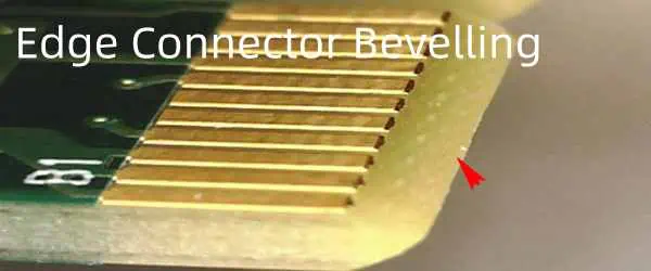
Edge connector Bevelling
Beveling refers to a process of minimizing or reducing the square shape edges of a PCB to get sloping sides. In PCBs, the process of beveling usually takes place right after the soldering mask and before starting the surface finishing. The main aim of the beveling of edge connectors is to make the insertion process easier, as it may become difficult to get easy insertion without beveling. Moreover, beveling is mostly done per the demands of customers and clients.
However, the bevel creates an angle of 30-45 degrees. As some printed circuit boards contain longer or large gold fingers, therefore, they need beveling to fit like one whole component. At the same time, most devices require connectors with certain measurements which enhances the need for beveling. Beveling plays an essential role in an edge connector. It makes sure that gold fingers fit together in a place easily. Moreover, it leads to failure if the parts do not fit together.
The connection point of PCBs constantly faces plugging and unplugging as per the role and nature of interconnecting boards. Therefore, without a reliable contact edge implies, the board becomes sensitive to constant plug or unplug situations. This may lead to a malfunctioning device. At the same time, gold plating on almost all connectors helps in enhancing the durability of PCB edge connectors. However, gold comes at higher prices. Other metals like copper can work as an alternative to gold, as it offers various benefits.
Due to higher electrical conductance and higher resistance towards corrosion, gold is considered the best metal of all. Moreover, it easily allows making an alloy with cobalt or nickel, which enhances its capacity to bear overuse even after a very short period. Many experiments have been conducted to examine the ability of gold to be resistant to other metals. This shows that gold contains the lowest level of resistance among all other metals. In addition to this, gold gives a solid connection that does not allow oxidation or any interaction with other metals.
What Are Chamfering Of Edge Connector Bevelling In PCB?
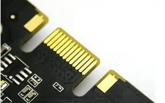
The edge connector serves as the female connector. It creates a connection with the PCB contactpads, which line the edge. Just take a second and think about those PCI slots to put memory cards in and how they make easy ways to insert the car in the PCB motherboard. When the product allows hardware upgrades, then edge connectors refer to the standard interface.
It’s a designer’s duty to ensure that the board can mate easily with a standard connector over the matting panel. And here, chamfering steps in. Make sure that the PCB mating edge connects the angle of the chamfer and tolerances that the connector manufacturer has specified. In addition to this, ensure that the manufacturing contractor must have the capability to meet all the angles of chamfer and tolerances you want.
What Are the Limitation Of Edge Connector Bevelling In PCB?
The gold finger method considers a significant technique. Unfortunately, its applications have limitations because of several reasons. For example, plated pads must come at the circuit board’s edge. As gold plating needs an electroplating method, it must make the connection that joins the frame of the panel and plated pads together. The manufacturers that create fingers with a length of about 40mm also create these plating pads. However, if you need gold fingers longer than this, then the manufacturing process becomes complex.
However, it does not end here. You must know that the PCB edge connector’s internal layer must not contain copper. If it does contain any copper, the beveling process of the connector will expose all the copper. Moreover, other than flex PCBs, while gold plating both PCB sides, make sure the distance between both the upper and lower layers of the PCB must not exceed 150mm. At the same time, its max length must not surpass 40mm.
Moreover, the length of the gold finger may increase or decrease in some cases. It implies that pads with shorter lengths will connect vertically with the gold plating bar, a factor that may affect functionality.
Edge Connector Bevelling – Application Of Gold Fingers
Gold fingers play a significant role in connecting two adjacent circuit boards with each other. In addition to high electrical conductivity, it protects the contact edge from overuse and enhances its durability. Gold offers various functions and features. However, gold fingers are used in many devices, and a few benefits it offers involve the following.
The foremost use of the gold finger includes the beveling of the edge connector. Gold fingers allow easy installment of additional attachments within the PC or circuit board.
Moreover, it is also used in interconnection points. It creates a connection between the several enhancements and the motherboard using PCI, AGP, and ISA slots. Gold fingers help in conducting signals among computers, cards in the slot, and peripheral devices.
Furthermore, it is used in external connections. It allows the creation of external connections, particularly in computerized industrial applications and machines.
Conclusion
The bevelling of edge connectors refers to a type of process that cuts or shapes the PCB edge connector over a specified angle. The beveled connector or PCI makes the installation of components easier. Moreover, it refers to a parameter and often requires making a perfect fitting between gold plating fingers in the board.
EUR files are important to understand when you are learning about computer terminology. Some people find it hard to learn about EUR files and eventually end up confusing themselves and giving up on them. Also, you will learn how you can access the EUR files on different operating systems.
Plus, did you know that you can open EUR files on iOS and Android? Not really? Well, this post is going to be interesting for you. Today, we are not going to let you give up on EUR files, as this post discusses all the major aspects of EUR files in detail for you. So let’s get started without delay!
What is a EUR file?
You define the EUR file as those files that contain a special EUR extension (dot EUR). Now the purpose of these files is to let the mobile applications know which files they can easily access. These files are different for every application and contain a different and unique set of data as well. EUR files have confused several users by far, and there have been many cases in which users have struggled to open these files. Therefore, let’s see how you can open EUR files easily.
Before, we start, you need to remember that the EUR files are different for different applications. These mobile applications or programs can use the EUR files for variable purposes. Therefore, you need to be specific with the EUR files. Or else these files won’t open, and you will keep scratching your head at the same time. So, you need to use a EUR file opener, and here’s how you can leverage it for your purpose:
Steps:
Begin by tapping the start button.
A window will pop up showing “search for programs and files.”
Now tap “Regedit” and press the “enter” option.
Carefully use the CTR+ F key for accessing the EUR extension.
You can do the same step by opening the edit menu and going to the “find” option.
Now mention your preferred EUR file on the search bar.
Tap Ok and then Enter.
Considerations
Using a EUR file opener is not enough; you need to be careful while using it, or else it will just waste your time. Some scenarios can complicate using this type of software for you as well. So let’s quickly learn about the considerations below:
You must not make alterations to the windows while using the opener since it can delete and compromise your critical data and might collapse the OS. You won’t be able to recover.
Always prepare a backup copy of your registry so that your data will remain safe in case of any changes and you won’t lose your important data.
You can also create multiple entries with the EUR extension, and you can easily do this by navigating to the context menu/edit menu on the dashboard.
Once you have completed the EUR extension entry, don’t forget to shut the system down so that you can restart the system whenever you want without any complications.
Possible Problems With The Eur Format Files
If you are struggling to work with the EUR files, then it does not mean that you lack skills. It just happens due to a lack of information. Here, we are giving you certain information that will address all your issues with the EUR files. Sometimes, it does even happen due to a faulty computer or the software you are using. There can be other reasons that you need to know:
The EUR file has been corrupted.
The entries contain invalid links to the EUR files.
You have an incomplete installation of software that contains a EUR extension.
There is malware attached to the EUR files.
The hardware of your PC is not updated, which is why it cannot support the EUR files.
You are using outdated and dysfunctional drivers.
Note: These are the common reasons that your EUR files are giving you a hard time. Other than this, if you are still unable to find out the real cause or the existing problem persists, you need to consult professionals to solve the problem.
For Windows: Right-click on the EUR file you are working with, which will show an option saying “open” and then click that and then select “choose different application” Now you need to see which software suits you the best and make sure to select the option “use the application to open” to save time.
For Mac: Right-click on your EUR file, click “open with,” click “other…”, now choose your preferred software and make sure to tick the check box.
For Linux: Repeat the process described above to access your EUR files.
For iPhone: Click on the EUR file, and click “share,” which will let you select a suitable app for the file and then save your EUR file and make sure of it, now open the files app, press and hold the file, remove your finger, it will pop up a menu bar, tap on “share” from the menu bar and then choose an application that you like.
For Android: Go to your mobile’s settings, access the “app section,” and tap the “options” from there if you need to switch between the apps.
Software Update
Sometimes, ignoring the updates can give your EUR files give you a tough time. Due to this, always update the software for opening the files.
Checking EUR files
The EUR files only work if they have not been corrupted or they do not contain malware or virus. Therefore always check your files with an anti-virus scanner.
Conclusion
There is no doubt that EUR files are important, and accessing them in time becomes inevitable in most cases. Technical issues like virus invasion, file corruption, and computer hardware problems can complicate accessing these files for you. We have discussed how you can access EUR files on different operating systems. Make sure to follow the instructions completely to work successfully with the EUR files.
Do you know that it is possible to combine two or more antennas to provide a desired function? Perhaps, this is your first time of hearing it and you are wondering how possible it is. Well, it is possible because of the term called combination antenna.
This article is a guide to understanding what it takes to combining two antennas – or even more. You will also discover some of the different possible combinations you could make.
What is Combination Antenna all About?
Also called antenna combiners, the concept refers to the integration of antennas with different operating frequencies in one housing. This process became process for a couple of reasons, which would be explained further in this article.
Have you played the video game, “Need for Speed?” If you have, you must have realized that it is so-called because of the need to speed-up the cars to win the race.
In a similar perspective, there is a need for antenna signal combiners – the need to scale the rate at which frequencies are distributed. These combined antennas are capable of amplifying multiple frequencies almost at the same time.
Types of Bands Amplified
The two-antenna combiner can amplify the frequencies of different bands and frequencies. Examples of these are:
The Design and Construction of Combination Antennas
Also called multi-antennas, the combined antennas have a sturdy presentation. Here are some of the things you need to know about the design and construction:
1. One Housing
The different antennas and the components are housed in the same place called the radome. These are some of the radome’s specifications:
It can be made from rigid plastics, such as ABS.
A polyurethane foam is used to protect the radome’s radiating elements from physical impacts.
2. Cables
These cables serve as the cable and antenna combiner, whereby they are used to tag the different antenna elements. This way, it is possible to make an individualized identification of the different elements when the lines are being routed during installation.
3. Feedline
You will also find individual feedlines for each of the antenna’s elements. These elements work as separate antennas and leverage the feedlines for striking a connection to the downstream circuits and radio devices.
4. Combo Antenna Elements
The elements making up the combination antenna also play a role in the performance. Depending on the application, you could have up to 11 elements connected in one radome.
Before we dissect some of these elements, let us have a few points about them:
The elements could operate as separate or individual antennas. In this case, the elements rely on the feedline for connecting the radio devices and circuits.
The number of the elements vary based on the technologies served. If you are connecting the core technologies, it is possible to use up to 11 combined antenna elements.
It is also possible to use supplementary combined antenna elements. Such is the case when connecting either the multiple bands or 2×2 MIMO networking.
Here are the different types of elements or components you can find in combined antennas:
Ground Planes
These elements are added into the antenna design as a way of providing a metal sheet at the antenna’s base.
Feeding Pads
These are responsible for transferring the electrical signals between the transmission line and the antenna element.
Antenna Radiators
These are the combined antenna elements that guide the Radio Frequency (RF) energy by acting as the transducers.
Low Noise Amplifier
The Low Noise Amplifier (LNA) enhances the signals coming from the GPS.
Ground Pads
These are used to make an electrical grounding of the combined antenna’s elements.
Fixing Pads
These are used for facilitating the anchoring or guiding of the different elements within the radome.
Radome
This is the ceramic housing for the combined antennas. The primary function of the radome is to provide excellent thermal protection anytime the ceramic antenna elements are in use.
Multi-Antenna Installation via Through-Hole Mounting
The installation process for combined antennas is a bit technical, which is why you must be careful how you go about it.
The through-hole mounting process is often preferred for this purpose, because of the streamlined process.
Here is a breakdown of all that goes into the through-hole mounting process for combined antennas:
Hole-Making: the first step is to drill a hole on the surface where the antenna is to be mounted. It is common to make these holes on reachable surfaces.
Secure the Antenna: you can then secure the antenna by using any of the following: gasket seals, a washer, a threaded hollow bolt or any other material that can hold the hole securely.
Pass the Cables: remember that combined antennas also use cables. Now, you have to pass the low-loss Radio Frequency (RF) cables, one from each of the antenna’s elements.
Cable Connection: once the cables are passed, proceed to pass them through the bolt. Once that is completed, you can then connect the cables to the wireless equipment.
Alternatives to Combination Antenna Installation
It is possible that the traditional mounting process of the antenna doesn’t interest you. Other options exist and we are going to talk about them in this section.
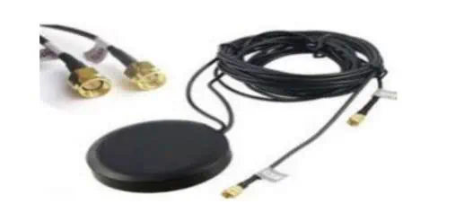
Puck Combo Antennas
This is named after the radome’s “hockey puck shape.” The puck combo antennas can also combine with the through-hole mounting process.
Here are some of the processes involved:
Hole-Drilling: the first step is to drill a hole, where the puck antenna will be mounted.
Puck Antenna Placement: step two is to place the puck antenna over the drilled hole.
Component Placement: the rest of the components, including the antenna cables can then be run through the pre-drilled hole.
Puck Security: make a screw-mounting on the antenna to secure the puck antenna inside.
Puck Combo Antenna Features
Here are some of the attributes of the puck-shaped multi-antennas:
Waterproof Skirting: this is an additional measure meant to protect the antenna from moisture ingress.
Direction Considerations: puck-shaped multi-antennas can have different directions, such as omni-directional (getting signals from different directions) and directional (getting signals from one direction).
Magnetic Mount Combination Antennas
Consider using the magnetic mount process to combine two antennas (or more). It is an excellent option to the through-hole mounting process, which is a bit rigid.
Here are some attributes that make the magnetic mount combo antenna design unique:
Multi-antennas only need to be set in the right positions, instead of making holes.
The flexibility of making changes to the sitting position of the antenna or even removing the antenna is there.
Magnetic Mount Connection Process for Multi-Antennas
Multiple antennas can be connected at the same time, thanks to magnetic mount’s set-up process. The procedure includes the use of a metal surface to secure the combination antenna to the base.
The process also uses a brass terminal insert for connecting the multiple antennas. Depending on where you want to place the antenna, it is possible to use length of coax cable to extend the height. Note that the coax cable’s length often terminates or stops at the FME.
The Leading Wireless Technologies Powered by Combination Antennas
Multiple antennas can be used to boost the performances of a wide range of wireless technologies. The list of these technologies ranges from Wi-Fi, Cellular, 3G, 4G, 5G and GPS. Even GNSS is also supported.
We will now look at some of the combinations that can be made out of these wireless technologies.
GPS + 4G + Wi-Fi Antenna
This is the combination of the Global Positioning System (GPS), with the fourth generation of wireless technology (4G) and the Wi-Fi network.
It is a 3-in-1 type of combination antenna. Among many other features, this combination supports 4G LTE, up to 2.4GHz for Wi-Fi and has a frequency with the GPS.
Getting the three in the same radome comes with a lot of perks, such as:
Finding a suitable use case in objects or devices that find it hard to transmit signals due to the content of their base materials.
This 3-in-1 multi-antenna makes a good option for the track and trace systems especially for generators and vehicles.
GPS + Wi-Fi Antenna
This is another combination antenna variant you can find. It only supports the interconnection of the Global Positioning System (GPS) antenna and the Wi-Fi antenna.
The GPS antenna works by receiving and amplifying the radio signals that are distributed/transmitted on specific frequencies. These signals are received from a GNSS satellite and are then converted to an electronic signal for the GPS receiver’s usage.
On the other hand, the Wi-Fi antenna works by converting the Electromagnetic Waves (EM) into electric signals. It can also convert the electric signals into Electromagnetic Waves (EM).
Differences between GPS Antenna and Wi-Fi Antenna
The first point to note is that these antennas ordinarily provide different connections. On the one hand, the GPS antenna converts radio signals into electronic signals, while the Wi-Fi antenna converts the Electromagnetic Waves (EM) into electric signals.
The second difference between the two is that the GPS uses satellites that orbit around the earth for real-time triangulation of a user’s location. On the other hand, the Wi-Fi’s locating technology gathers relative network signal strength from different network access points.
The third difference is based on the individual lengths of the antennas. To put it into perspective, this has to do with the frequency bands. For example, the antenna length and tuning for GPS receives frequencies at different bands, such as:
1575.42
1227.6 and;
1176.45 MHz
The length and tuning of the Wi-Fi antenna are usually optimized for the ISM bands that support Wi-Fi at either the 2.4 or 5 GHz.
4G + Wi-Fi Antenna
It is also possible to combine the Wi-Fi antenna with the fourth-generation wireless technology (4G)’s antenna. For the best signal receipt and transmission performances, you want to cross-check the frequency of the 4G antenna with that of the Wi-Fi antenna.
Considering that Wi-Fi antennas are tuned to either the 2.4 or 5 GHz bands, you want to make sure that the 4G antennas are closer to that. Therefore, a 4G antenna that has up to 1.9 GHz frequency band might suffice for the interconnection of the two antennas.
You can combine two antennas for better reception and this helps your device get better signals. If you must choose one, here are certain criteria to consider:
1. Select the Right Connector Type
The type of cable or connector used for the combination is very important. The cable refers to the Radio Frequency (RF) cable that serves a transmission line for the RF signals that connect to the receivers and transmitters. On the other hand, the connector enables the mechanical connection between the Radio Frequency (RF) system and the antenna.
2. How Many Combinations are Needed?
You have the option of choosing from a vast selection of multi-antenna combinations. Your choice can be anywhere between the 2-in-1 and 11-in-1 combinations. The number of multiband combinations is directly proportional to the number of antennas you want to connect and the range of the purposes they are meant to serve.
Final Words: Combination Antennas Lead the Way
Combining multiple antennas in a single housing (radome) has become one of the trends shaping the means of communication in the modern world. From our homes, offices and vehicles – we can install combined antennas to improve the wireless signals into our devices.
With the possibilities of combining 4G, Wi-Fi, GNSS, GPS and other wireless technologies; the opportunities are just endless. Depending on the configurations (from the 2-in-1 antennas up to the 11-in-1 antennas), you can extend the coverage of the signals and connect more devices.
Choosing the right combination antenna is a must, as it helps you get high-speed data transmission, real-time signal reception and quality network coverage. With this in place, you can then deploy your multi-antennas for use in different applications and industries, such as in and around your vehicle, at home, in the office, for vehicle tracking purposes and fleet management.
What happens when one of your five senses fails to act properly? You won’t be able to taste your favorite food and smell your favorite flowers! In physics, sensors do the same job. Electronics need sensors so that they can detect what’s happening around them. Willem Von Simens invented the first-ever temperature sensor in the 80s. After this invention, other physicists brainstormed some new versions of sensors.
Later, the IR sensors came into being in the early 90s. Since technology has been advancing at a rapid pace, we all know that new inventions are more important than ever to stabilize the economy of countries. Today, critical domains rely on different types of sensors that detect humidity, smoke, and motion. Two broad categories of sensors are analog and digital. However, due to time constraints, we won’t be able to inform you about all types of sensors. So we have picked touch sensors to discuss in this post.
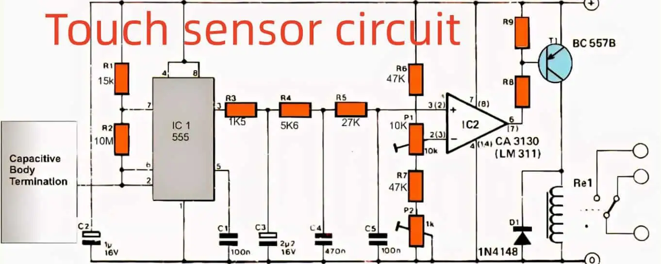
What is a Touch Sensor Circuit?
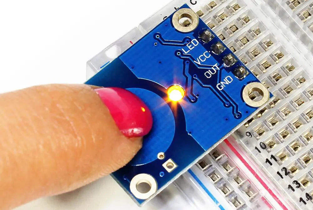
Touch Sensors are incredible devices. We say this because you can use such sensors when you want to sense touch through your devices. Pretty obvious, no? They mainly work as regular switches when you touch them to turn them ON and OFF. These are important for their interface, which is intuitive. You can also call touch sensors tactile sensors.
They are reliable to be used in the place of switches
Types of Touch Sensor Circuit
Capacitive sensors: These are for determining the capacitance of your devices and are mainly useful for small and portable devices. These are heavy-duty and endure abrasive damage to a large extent.
Resistive sensors: These sensors do not need any magical electrical characteristics for fine performance. Their job is to detect the pressure on any surface under observation.
Principle of Touch Sensor Circuit
Touch sensors have a special working principle that they follow for natural performance. Their working principle is not different than that of a switch. When you will touch them, or they will detect some pressure, it will trigger the sensor, and it will perform just as a closed switch does. When you remove the pressure from the sensor, it will behave like an open switch.
Working of Capacitive Touch Sensor Circuits
If we talk about capacitive touch sensors, they consist of a pair of parallel conductors. There is an insulator placed between these conductors. The conductor is actually our capacitor in this case. When you touch the sensor, the plates also interact with your touch. It will boost the capacitance value since our fingers are a conductive entity for the sensor. The default value of the capacitor is C0 which means it will change as there will be some change in the capacitance.
Working of Resistive Touch Sensor Circuit
Now let’s discuss resistive touch sensors. In this case, their job is to detect the pressure, right? So, they will determine the amount of pressure on a particular surface so that they can sense the touch at the same time. There are also two conductors present in resistive touch sensors, like capacitive sensors. The plates have a layer of indium tin oxide that serves as an excellent conductor. However, there has to be a little space between these plates. There is also voltage present between these plates. When you apply the pressure on the surface, it will be sensed till the bottom of the plates. It reduces the voltage, and the sensor detects it impressively. This is how it uses pressure to detect the touch in general cases.
Applications of Touch Sensor Circuit
If you still don’t know how touch sensors contribute to making our daily lives easier, we are going to discuss their applications in this section. Let’s see them below:
Touch sensors can be used to determine distance and pressure in the construction of devices.
Resistive touch sensors are useful for detecting little pressure and touch and have applications like touchpads and keypads.
Demerits of Touch Sensor Circuit
Sometimes touch sensors can undergo glitches which can make them produce false results like false alarms. Due to this, it is important to understand their maintenance and use reliable and industrial-grade touch sensors every time.
There are some standard touch sensors that most producers rely on. One of them is the 4017 IC. We are going to see how it performs and what makes it so special to be a producer’s first choice!
There are normally 5-10 outputs in most of the ICs.
The output begins from pin3 and ends at pin11; however, this can be different as per the type of the IC.
This range contains all the outputs that play their role in transferring higher logic throughout the pins whenever a single pin detects a positive pulse.
The sequence does not necessarily have to end at the last pin, which is pin11. You can stop it whenever you want at any pin.
You need an extra pin15 so that when the sequence reaches this particular pin, the cycle must stop. The new cycle will be the same, and the sequence will follow the same order as well.
Working
One thing that induces the cycle is when you touch the plates. It creates a positive pulse that shows up at pin14 when you will touch it. Now, imagine you have turned ON the switch, and the higher logic is present at pin3. You have not connected the pin to anything yet. At the same time, you have connected the pin2 with the relay.
Right now, the relay is OFF. When you touch the plate, the positive pulse of pin14 will generate the output sequence that goes from pin3 to pin2 and turns ON the switch. It is fixed and does not change with the relay and the load. When you touch the plate for the second time, the order of the sequence will be pin2-pin4 which means it will persuade the IC to change the logic at pin3. It will turn OFF the relay and the load.
If you are an electronics maestro, you would be well-familiar with the importance of current sensing for constructing electronics and other devices.
Current sensing is a crucial step that not only allows you to adjust the current levels but also protects the devices from potential risks of damage and failure. You need to sense the current to analyze any electronic device.
Small to big applications use current sensing for this purpose. Your mobile charger also senses current among its different components. Now, you get different types of current sensors as per your requirements. These have different current sensing methods based on the use case.
One of the common methods followed by many sensors is the shunt current resistor. We are going to explore a shunt current resistor in this post and see what makes it an important sensor for various applications of our lives!
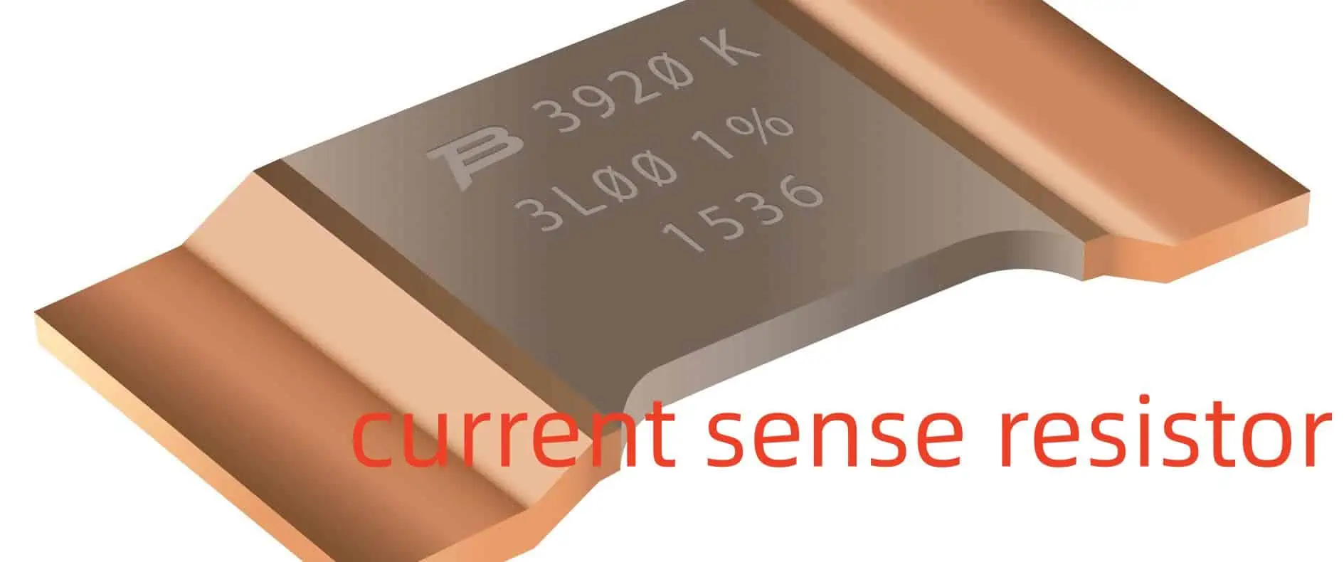
What is Current Sense Resistor?
A Current Sense Resistor works similarly to the standard resistors. You might be surprised to know that its resistance is incredibly low compared to its variants. The power offered by this resistor is higher than the others. You position these resistors in the middle of the current route. Now, determine the changes in the voltage and insert the values in Ohm’s equation. V=IR or I=V/R.
After this, you will get the amount of the current that you have been working for. To describe it in simpler words, a shunt means you are making a new path in the circuit. The same is what the job of a shunt resistor is. These make paths for low resistance. So that the current can keep going from one area of the circuit to the other without any disturbance, you can easily detect the amount of current flowing accurately even if it crosses a low resistance region. All this is due to a shunt current resistor!
Parameters of Current sense resistor or Shunt Resistor
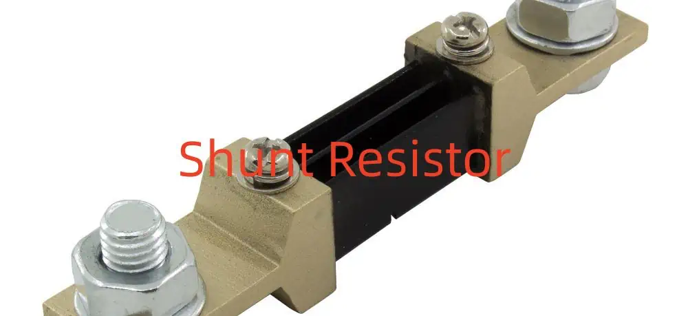
Shunt Resistor
You must know that you cannot take full advantage of a Shunt resistor without considering some parameters. Ready to know about these? Let’s check them out below:
The temperature coefficient of a shunt resistor is higher than the others because these allow a higher degree of current to pass.
You can determine the thermal EMF of a shunt resistor based on the temperature, unlike other resistors.
You need to carefully choose the type of shunt resistor by weighing down its production material.
Different elements have different thermal EMFs. Manganin’s EMF is different from Copper’s.
Managing is a suitable material to create a blade shunt resistor since its EMF is useful to make this type of resistor only.
Power Rating of Current sense resistor: Power Rating and Resistance
Resistance and power rating are some of the important factors affecting the Shunt resistors. These directly impact the voltage changes when the current makes its way through the system. You can use a current sense amplifier to get the data.
It will work with the full range of the current and input voltage to give you the value of the shunt resistor. If the value is too large, it will influence the power rating, which will lead to excessive heat dissipation than before.
Tolerance of Current sense resistor
You might know this fact; electronics do not submit to ideal situations. Shunt resistors do the same. Since we are talking about tolerance, shunt resistors cannot perform precisely without accurate tolerance. If you consider, you will come to know that regular resistors have a tolerance of up to a maximum of 10% and a minimum of 1%. It is an advisable range to use in major applications.
So if you change the temperature, it will change these percentages as well. When you are only relying on a sensed value, you cannot overlook the role of tolerance for it. The tolerances of these resistors that offer sensed values like shunt current resistors range to 0.1% only. Now, it depends on your project how much will be the accurate output, and you must select an appropriate resistor as per your application. So make sure you are keeping these considerations in mind before hopping onto your projects. It will save you time and prevent failure from taking your peace away!
Temperature Coefficient of Current sense resistor
TCR helps you analyze what amount of the resistance will undergo change when you increase or decrease the temperature. It is another important parameter that can badly influence your output if not considered precisely.
For all the shunt resistor devices, TCR plays a great role in the precision of the devices. You need to make sure that the TCR remains low as much as possible when you’re working with a shunt resistor. It is because these resistors allow huge amounts of current to pass through. Because of this, the system will let out more power through dissipation.
After this, the temperature of the resistor also skyrockets. Now all these changes can impact the resistor value, leading to faulty readings and more chances of human error. There are certain materials that influence the TCR as well. You can also call them resistor elements if you are considering power rating and tolerance for your applications. You can find several low TCR shunt resistors out there. The TCR value of such resistors is low because they contain special metallic foils that serve to reduce TCR.
By far, you know much about the importance of a shunt resistor. But sometimes, different applications require a different type of shunt resistor. Some users fail their projects since they do not know how to choose a shunt resistor for their projects. However, you won’t be from them because the next section is going to discuss this with you!
We told you that you could be overwhelmed by the large variety of shunt resistors present in the market. So how would you choose the best shunt resistor for your projects? It’s not something to worry about! We are going to spill some tips for you to get the best shunt resistor for yourself:
Determine the current of the resistor and see if it’s suitable for your device or not.
Check the voltage rating of the resistor for the application.
Make sure to study your application fully before selecting a resistor.
Some shunt resistor models are for fast testing of the devices, and they are only efficient for this purpose.
You also need to determine the input voltage of the application, especially in the case of a current amplifier.
Shunt resistors that read in milliohms can prove to give accurate readings.
Now you need to determine the power rating as well so that you can consider what amount of power will go into dissipation.
Remember this thumb rule: if the value of the resistor is less, the power rating will also be less.
Lastly, you should know about the tolerance of the shunt resistor. We recommend you choose a resistor with a tolerance of 1% for your applications.
Some applications need an extra kick of tolerance, so you need to grab appropriate resistors for them.
Also, you don’t want to forget about the package. It will help you with the soldering when you are working with smaller PCBs since these have tight and hard-to-reach areas. Resistors with extremely less TCR are befitting for this purpose.
The performance of the PCBs depends on their design. Imagine a PCB design with errors in its functioning. Now what happens? It will lead to complications, and your clients might get angry with you as well. PCB designs are the building blocks which means the structure of PCBs is important to consider. You cannot expect great performance from PCBs with faulty design. It becomes more important in miniaturization.
Small PCBs are complex, and their designs need perfection at the same time. To handle this easily, today, PCB producers use EDA, which means electronic design automation. These platforms are just like tools to make PCB designing a lot easier. We are going to discuss two common EDA tools right here in this post! Let’s learn about these!
Kicad EDA
We have KiCAD here, which is a fine EDA tool that will make PCB designing a smooth sail for you. It is a free EDA platform and enhances the quality of designs of PCBs. It is open-source software. Now, this means you can easily use it for help. Debugging your designs and PCB design optimization is also simple with KiCAD. You can use it on iOS, LINUX, and Microsoft with utmost ease. The list of KiCAD’s features is long; we will learn about these in a bit. However, we are going to take a look at the sub-modules that KiCAD offers:
PCBNew for Layout & Routing: You can rely on KiCAD for layouts and routing of PCBs. It happens because one of its submodules is called PCBNew. It speeds up the routing and saves you time. Further features for routing include obstacle avoidance and more.
Eeschema Schematic Capture: It is possible due to KiCAD’s called Eeschma. It offers schematic capturing in an efficient way. It uses UI to make your design spree productive. The file exportation is also simpler with this module. It supports different file formats as well.
Hierarchical Features: It comes in handy when you are considering complex designs. For example, multi-layer schematics. It will change your schematics into a fine hierarchy so that you can work on your PCB designs effortlessly.
Design & Electrical Rule: You cannot approve your designs without checking them. Rule checking of PCB designs comes in handy. It is because it will rule out chances of faults, electrical failures like short circuits, and current leaks. You can do this with KiCAD’s DRC tool. It will discover the errors so you can fix them in time.
3D Rendering: KiCad’s 3D viewer will help you with the 3D visualization of your designs. So that you can take a better look at your PCB’s structure, you can enhance your designs with 3D sketches from different angles.
Intuitive UI: The UI of KiCAD is dependable for productivity. It is important for the users so that they won’t get stuck with the navigation of the tool’s interface. It saves their time and improves their PCB designs.
Free Cross Platform: KiCad is a free, open-source PCB designing tool that comes packed with so many features. It runs on all types of operating systems as well. You will hardly experience any glitches and problems with KiCAD due to its recent upgrades.
Online Library: The users need to export and import files when designing PCBs. Therefore, you can rely on its fast importing/exporting system for this purpose. It has an online library with pre-existing templates to give an edge to your PCB designs.
What is special about KiCad?
If you are new to KiCAD, you might be wondering, what makes KiCAD so special? Why give it a try? Well, this is natural to think. Since KiCAD’s hype in the PCB world is incredible. So here we are going to see why you should actually start using KiCAD for your future projects:
First off, it’s free, unlike other PCB designing tools.
It comes packed with different sub-modules to outshine your designs.
The tool has no hidden costs.
No additional spammy downloads
Fast PCB designing to save your time
Who’s it for?
KiCAD is beneficial for mid-range brands. It is also a beginner-friendly tool that helps in better understanding the PCB designs as well. However, this tool might be lacking in features that do not make it a great choice for everyone.
Is KiCad EDA worth it?
KiCAD is a multipurpose tool when you want to handle different aspects of PCB designing. It is a one-stop solution when you want to improve your designs and fix problems in them. It gives you an edge by being a multifunctional tool so that your PCB designs won’t suffer from any complications.
Disadvantages of KiCAD:
We have listed some of the major cons of KiCAD, have a look:
Autodesk EAGLE is another EDA tool, perfect for your PCB designs. It has been making PCB designs seamless for the user since 2016. Autodesk has made many upgrades in the system so that it will efficiently improve the PCB designs. So what does it mean? It means an easily applicable graphical layout editor. The name says it all! It’s all about providing ease when you are dealing with complex designs. It has multiple features, and each of them describes its versatile nature. You can use a single Autodesk EAGLE for managing your designs with the least hustle.
Key Features of EAGLE
Advanced ERC & DRC: EAGLE is supportive of ERC and DRC. The users have cherished its rule-checking features to detect the faults in the designs and fix them in time. It ensures the protection and safety of the users and devices once the designs have been completed.
New Routing Engine: The routing engine of EAGLE has developed as well. It offers fine obstacle avoidance when you need it the most. It helps in route optimization and PCB navigation much easier. It comes in handy when you are developing a complex PCB design.
Design of High-Speed Features: High-speed design is important when you are running out of time and need industrial-grade PCBs. It has a bunch of unique tools that will help you outdo your designs whenever you use them.
3D Viewing Capabilities: EAGLE is amazing with 3D viewing and rendering. You can precisely check out your designs from different angles through EAGLE. So that there will be no chance of any failure at all.
Supply Chain Management: EAGLE also helps you with supply chain management. You can speed up your designs with its library and design templates. It also greatly reduces the production cost when you are handling bulk designs.
BGA Fanout Router: It also works suitably when you are looking for BGA PCBs. It supports the HDI so that miniaturization can take place without any complications. It has a dedicated tool for this purpose as well.
Reusable Design Blocks: You can also reuse your designs in the form of modular units of EAGLE, which are actually the shapes and blocks of your old designs. Just drag and drop these modular units, and then you will have your new design developed in just a few minutes.
SPICE Simulation: EAGLE never goes wrong with its precise analysis and simulation for your designs. It deeply inspects the PCB’s performance and matches the design requirements as well.
What is special about Eagle?
So why choose EAGLE when you can find tons of other PCB designing tools available? That’s a valid question. Let’s check out the answers:
EAGLE is good for designing complex PCB designs
It speeds up the designing process due to its libraries.
EAGLE is an effective tool for improving your PCB design quality
Who’s it for?
You can rely on EAGLE if you are an experienced PCB designer since it has some critical features that only need a veteran to understand. However, if you are a beginner and want to use EAGLE, then don’t fret. You can still use it for beginner-level designs quite easily.
Is Autodesk Eagle worth it?
That’s another good question. Is using EAGLE really worth your time and energy? Autodesk has made sure of it due to the latest upgrades in EAGLE. You can use it for FREE on the basis of its trial and see if its suits you or not. If it does, you can invest in EAGLE and see the incredible transformation of your PCB designs from boring to irresistible in no time!
Disadvantages of EAGLE:
You need to be aware of the downsides of this software so that you will have a clear picture while choosing between the two:
EAGLE is not good in fast speed digital transport
Wireless routing and lodging might not be up to the mark.
The free version is limited in providing features.
The user interface might be difficult in terms of ease.
It can be difficult to use for novices in some cases.
Main Differences Between Eagle vs. Kicad
You can use EAGLE for annotation and editing. Besides, it also offers sync that KiCAD does not, which helps with the designs and schematic.
KiCAD is a beginner-friendly tool, and it also assists beginners with their projects with a much more basic interface, unlike EAGLE.
KiCAD is more affordable than EAGLE because it is a free tool, while EAGLE is a paid one and only offers a FREE trial.
EAGLE is supported by MCAD viewing, which is an in-built feature; therefore, it is more reliable for 3D rendering than KiCAD.
EAGLE cannot transform your design’s schematics into a hierarchy, but KiCAD does.
EAGLE is recommendable when you need to go in-depth with analysis and simulations, unlike KiCAD.
Complex PCB designs are also easier and faster to develop with EAGLE.
You can trust EAGLE for BGA routing for HDI PCBs, where you need to play carefully with the high-density interconnects. This feature is absent in KiCAD.
It is a never-ending debate. Both tools have their strong points. It will definitely get harder for you to choose one from them for your projects. However, you need to be wise when choosing the best software. How’s that possible? You need to select the software as per your design’s nature. Experts recommend EAGLE for 3D rendering/viewing, effective analysis, and simulation purposes. While KiCAD is famous for its simple navigation and interface. It also can be your biggest asset when you are just getting started with PCB designing.
Eagle vs. Kicad: Who’s the Winner?
It mainly depends on your skills and the nature of your designs. Some designs don’t need EAGLE, which is an advanced tool. Whereas using KiCAD for some projects won’t render positive results. To draw a fine line between the two, if you are a beginner, go for KiCAD, while EAGLE is for the veterans. If you are someone who loves to customize their tool, then EAGLE is not much flexible with that.
So, Which One Should You Pick?
The answer just depends on your needs. What you are looking for in EAGLE and KiCAD determines your projects. Both software has some similarities, but their features ad functions are different at the same time. Therefore, which one you should pick depends on the type of your project. You even might have to switch between both since both have limitations as well. If you often work with complex PCB designs, then EAGLE will always be a great choice.
Conclusion
You are never going to end KiCAD vs. EAGLE debate. Both are important for PCB designers. As per their needs, both programs serve our PCB designers to the fullest. Due to this 5ereason, today, we are able to witness the marvels of PCBs due to their remarkable designs. All this is possible due to the features of such software. We hope that now you can easily choose between KiCAD and EAGLE for your upcoming PCB designs!
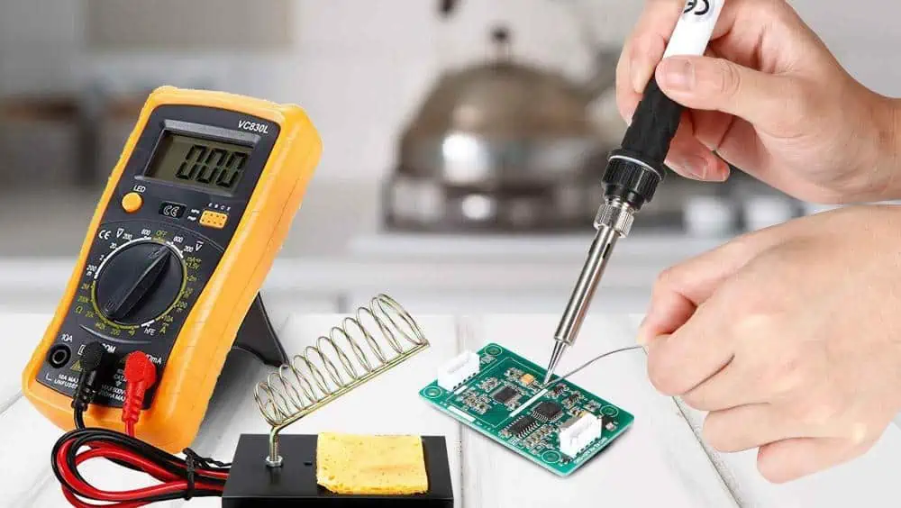
There are several methods of soldering, yet they all give the same result. It connects two distinct metals with the use of different types of solder material. Solder comes in a variety of materials.
The most common solder comes in metal alloy, which includes a mixture of tin or lead and brass or silver at very low MP. The solder starts melting when it comes in contact with hot soldering iron during the soldering process.
However, solder acts as an epoxy or glue that combines different parts of the board together.
The process of soldering on a circuit board or PCB refers to PCB assembly or PCBA. PCBA refers to a circuit board that contains copper plates, wires, and electrical components on it. PCBA plays an essential part in consumer electronic devices that we use daily. Consumer electronic products like smartphones, routers, computers, ovens, microwaves, refrigerators, and all contain PCBA in them. Moreover, it is also used in other fields of life like automobile, telecommunication, medicine, military, defense, and aerospace.
Types Of PCB Soldering Methods
PCB soldering refers to a process of combining more than two components together on the circuit board surface. Soldering plays an essential role in the designing process of a circuit board, as soldering is the only method to attach the circuit to a board or panel.
The three most common and widely used soldering methods involve Hand Soldering, Wave Soldering, and Reflow Soldering. Hand soldering, as the name suggests, performs manually, while wave and reflow soldering uses SMT or surface-mount machines to perform.
Hand soldering refers to a type of process in which humans apply pressure manually with a soldering iron pre-tinned tip. This heats up the solder and melts it.
However, hand soldering also refers to soft soldering in the field. It happens because hand soldering requires a temperature below 400 degrees Celsius. The metal alloy of solder contains lead in it which has an MP or melting point lower than 350 degrees. Volatile or fusible electrical components need less heat during soldering to avoid any damage. Therefore, make sure to use temperature at the lowest possible level so it won’t melt the metal. This, however, gives a “soft” connection or joint.
PCB hand soldering uses rework and Thermaltronics soldering equipment. It refers to the very last step of assembly, which requires complete details for SMT or THT components. SMT refers to a process in which components attach directly to the PCB surface. The device that uses this method to incorporate components serves as an SMD or SM device. At the same time, THT refers to a process in which electrical components are inserted in the PCB using holes and wires and soldered on the other side of the pads.
Moreover, hand soldering needs quite a lot of experience and knowledge to master the technique. The majority of engineers and assemblers consider it one of the simplest techniques. Yet it comes with both benefits and drawbacks.
Pros of Hand Soldering
Hand soldering allows the creation of a reliable electrical connection joint. Moreover, it is ideal, especially for smaller electrical components.
Cons of Hand Soldering
Hand soldering does not allow for higher temperatures. Therefore, it does not create a strong joint. Moreover, you cannot use it on devices with higher loads.
Hand Soldering & Assembly Rework
The process of hand soldering needs two main components to commence. A solder and soldering iron. Solder refers to a metal alloy that acts as an epoxy to joint components. While soldering, irony refers to a source of heat that melts solder around the electrical components. Irons come with different Watt ranges. Soldering irons with a range between 15W-60W gives good results. Moreover, a higher watt range may damage the board or the component.
Steps Of Hand Soldering
· Component Placement
Component placement comes as the very first step in the hand soldering process. First of all, clean the board to remove any type of dirt. Bend the wires or leads. Put the electrical component through the holes present on the panel. To ensure the right placement of the component, bend the wire from the board’s bottom at an angle of 45 degrees. Once the component fits in its right place, move forward. Extend the leads from electrical components to relieve their stress. Make sure the bend must remain two diameters of lead from the electrical component. The bend’s internal radius must equal one lead diameter. Also, the placement must show all the electrical parts.
· Preparing The Soldering Iron
Put the soldering tip on the joint in such a manner that it shows visible visuals of the contact point during the process of soldering. The angle must be 45 degrees. Make sure to clean the tip of the soldering iron and tin it well before using it. Furthermore, a freshly new tip that you have never used before must be tinned right after the solder reaches its melting point. Tinning refers to applying fresh flux and solder to the soldering tip. This coats all the soldering surfaces with the solder.
When the iron gets cold, wrap it with the soldering wire. Heat the soldering iron until the solder starts melting. Wait until the surface of the tip is completely wet. Wipe off any extra solder paste from the tip, then move on to the soldering. Also, remember if tinning does not complete efficiently, it may lead to an oxidized tip which makes the soldering process harder and more difficult.
To remove the oxidized part, copper tips can go with filing. However, the already-plated tip does not need any filling. Cool down the tip for a bit and use a wiring brush to brush off the stubborn brown or black oxidized material. Keep on brushing until the oxidized material removes. You can also use find files or sandpaper.
Once the oxidized material is removed, start the tinning process. Make sure not to sand or fill the plated tips. Moreover, if the tip does not have any oxidation and tin well, then just clean it with wipes, or damp sponge, or any other material before soldering. Place a tiny solder ball on the soldering tip surface, which helps as the contact point with electrical components in the soldering.
· Apply Heat
The iron tip of the soldering iron must touch the metal of the board and the electrical components firmly to create a connection. Apply heat on both parts until the solder melts down and gives off a strong joint. Put the solder around the electrical components. Take off the soldering tip as the joint form to prevent overheating the solder paste. Make sure to complete the process of soldering within just 2 seconds. However, if anyhow, the soldering takes 5 secs; then it may happen because of the incorrect method, small soldering iron, or too small soldering iron tip.
Make sure the tip of the soldering iron has a temperature of 343 degrees Celsius. Moreover, both metals must have a surface temperature above the melting point of the solder to accomplish efficient wetting. Make sure not to allow the solder to flow on a cooler surface than the temperature of the solder, as it may create “cold” joints. An adequate amount of solder flow and melt smoothly over the surface. Thus, giving a shiny, smooth, smooth straight thin edge. Whereas, if it gives a granular, irregular, dull, lumpy, and rounded look, then it means that the application of solder does not go well.
· Remove Heat
Once the solder coats the pad’s surface, stop applying more solder and take up the iron tip from the board. Do not touch or move the solder joint for about a few seconds. Allow it to cool down, as moving the joint will give off a cold joint.
· Finishing The Solder Joint
Cut off extra leads. Make sure not to fall for irregular solder edges. Also, leave a tiny headroom as it does not let the solder separate from leads on getting shocks during cutting.
Once you gather all the hand-soldering equipment and components, start the process with the following steps.
Clean the components leads and PCB thoroughly. Otherwise, it may create poor soldering joints.
Apply the solder paste on the electrical components and leads of the circuit board that needs soldering.
Heat the soldering iron at the required temperature.
Grab the soldering iron and soldering lead in each hand. In this, use a reel stand to maintain adequate tension and angle.
Identify the exact point where copper and leads of electrical components meet with each on the PCB. Put the soldering lead on that point and start applying heat.
Cut off the excess leads.
Look out for errors and irregularities. And try to resolve the problems.
Similarly, the soldering process works differently for SM assembly than the TH assembly. Do not lose hope if you don’t succeed in your first attempt at hand soldering. It considers the simplest method of all soldering processes, yet it needs extra care and attention while doing so. Therefore, keep practicing until you experience all of it. Hence, you will get a perfect joint PCBA in the end.
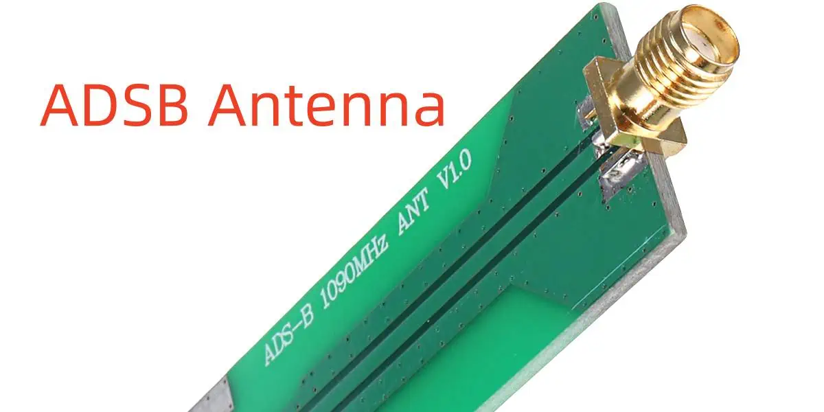
ADSB means automatic dependent surveillance-broadcast. ADSB antennas have vast applications owing to their features and fine performance. These applications are in the field of aviation, where this ADSB process supports multiple functions. These can include flight number identification.
Also, the flight direction becomes easier with ADSB antennas. You can even use these antennas for flight altitude and much more. It means without ADSB antennas, flights might lose their tracks as well. ADSB antennas are highly important for aircraft surveillance. Some essential components of such antennas include a receiver.
It also includes an aircraft positioning source. You will find a basic ground infrastructure, along with aircraft avionics as well. This technology has proven to be highly favorable for aircraft tracking, and one thing that makes all this possible is the antennas. It has a complex structure. However, special attention is important to develop such an antenna for safe and fruitful use.
So if you have no idea about how ADSB antennas work for aircraft surveillance, then don’t fret! We are going to take a look at the significance of ADSB antennas and their role in aviation in this discussion!
It is a special surveillance technology that helps to navigate the aircraft without any fatal mishaps.
Not just the navigation, this tech is reliable for aircraft positioning, determining the altitude of the flights and their speed.
Therefore, the ADSB tech works precisely with the radars so that the flights can take off and land in time without experiencing any damage and complications.
The ADSB antennas make this special tech happen and process the data through receiving and transmission.
Importance of ADSB Antenna in Electronics
These are the sole components of this technology, and it cannot survive without ADSB antennas when it comes to navigation and positioning of aircraft.
You can process all types of data needed for aircraft surveillance through ADBS antennas.
If you are wondering if flights can use this data for seamless navigation, then you are right, and this is possible just due to ADSB antennas.
ADSB antennas reduce the chances of crashes and mishaps in air traffic control through their advanced technology.
It is important to note that you will see different types of ADSB antennas out there. Because there is a huge demand for these antennas which makes them inevitable for aviation. However, one antenna cannot do the job of the other because of different features.
Considerations of Designs for ADS-B Antennas:
The design of an ADSB antenna determines its performance. It is obvious a poor design means a faulty ADSB antenna which aviation cannot afford at all.
So, in case you need to develop industrial-grade antennas, you need highly skilled engineers and technicians for this purpose. Or else, witness your system getting ruined due to defective ADSB antennas.
An industrial-grade ADSB antenna has a suitable radiation pattern. It also contains accurate gain. Now you know in order to develop a perfect ADSB antenna, you need to include accurate components for it. All the antenna parts have their individual roles in their performance and come together to make ADSB antennas useful assets for the pilots and air traffic control staff.
You should know that the size of the antenna will also influence its performance and efficiency.
If the gain is not accurate, it will negatively impact the signals.
Also, the radiation pattern needs to be precise, or else it will disrupt the signals and will also degrade the signals, which can lead to further complications.
Installation & Maintenance of ADSB Antennae
The installation of ADSB antennas matters a lot for perfect aircraft surveillance. Because the faulty installation will ruin their performance. Due to this, these antennas won’t be able to work at their finest. The technicians must fix the proper position of the antennas.
These antennas should not interact with any part of the aircraft as well.
The location of the antennas should be such that it will reduce signal degradation and mishandling as much as possible.
Therefore, to avoid mishaps, the antennas need proper grounding so that there will be no electromagnetic disturbance during data processing.
The dysfunctional antennas need a quick replacement.
Proper maintenance and optimization of such antennas are important to make them function impressively in the long run.
One of the major functions of ADSB antennas is to maximize the range and coverage, which greatly helps in aircraft surveillance. The maximizing of the range is hard to execute if the antennas do not determine the terrain. Identifying the obstacles also matters.
For the coverage, ADSB antennas need to be accurate and industrial-grade. Or else there is no guarantee that these antennas will be able to perfectly provide aircraft surveillance.
If we focus on the fuselage, then there are higher chances that we can increase the range and coverage of the aircraft through ADSB antennas.
Conclusion:
It will be unfair to not give all the credit to ADSB antennas. During the past years, aviation and aircraft surveillance has undergone many upgrades. There is no doubt that ADSB antennas stand as the most prominent upgrade of all time! Aircraft surveillance is now a seamless task because such antennas exist. These make your flights safe and sound. Keep the planes on a fixed track to reach their destinations. There are still many chances that ADSB antennas will become more advanced and efficient in the future.
FAQs
What is an ADS-B receiving antenna?
An ADS-B receiving antenna receives the signals during its functioning. Now the aircraft will transmit these signals and will use all the derived information from these signals. The information can be the aircraft’s altitude, position, and speed.
What types of ADS-B receiving antennas are there?
There is a huge variety of ADSB antennas available however, these are different in their features and prices. Therefore, the applications of these antennas are also variable. You can find a wide range of ADSB antennas in the market, but common types will be:
Directional antennas
Patch antennas
Omnidirectional antennas
How do I install an ADS-B receiving antenna?
While you install an ADSB antenna, it is important to pay attention to some considerations. Or else any negligence in the antenna’s installation will not let it from working properly. So the useful tips for this installation are below:
Ever heard of UWB antennas? Well, you might have, but still, UWB’s different aspects remain hidden from you. What does UWB antenna mean, and what it’s purpose? UWB antennas mean Ultra-wideband, which is a crucial part of telecommunication and can be anything that has more bandwidth than 500MHz. The UWB antennas never work with smaller bandwidths, and you can use them easily for the processing of complex and huge data. There are many industries around us that are relying on UWBs for IoT applications; computing machines and even wireless systems are using UWBs for fast, precise, and broad data transmission purposes. Tracking, placement, and location identification are much easier when you are using UWBs. We are going to shed light on major aspects of the UWB antennas for you in detail!
UWB Antenna Communication
People had no idea that UWB antennas existed until they got to know their use cases, like UWB communication. The UWBs are reliable for changing redundant technology, supporting the low-power communication system and frequency bands are all possible due to UWBs. You already know that when we talk about UWB wireless communication, we mean higher data rates and high frequency. Mishaps can happen when we are dealing with things on a large and complex scale. But UWBs save us from all the complications due to low-powered signals. Now its time to see why you should consider UWB technology:
UWBs have integral applications around us, meaning we might not be able to witness wireless communication, internet browsing, or video-calling with our friends at all without UWBs antennas. Not just this, UWBs are important for portable and smart devices that you mainly use at home and office. Experts believe that the world will witness impressive upgrades in UWBs with the passage of time. So that the users can draw out more desired results from UWBs for consumer electronics. Now, why are UWBs so acceptable among their users? Let’s see below:
These work on high data rates.
These are affordable.
These consume less power.
These are more reliable for sustaining broader bandwidth.
These omit the use of multi-narrow antennas.
If you use a single UWB antenna, it will handle the frequency, data transmission, and band operation impressively.
UWBs are reliable for controlling the multi-antenna interface and also consume less space.
Design of UWB Antenna
UWBs cannot work without an efficient design which means their body and structure matter a lot in their performance. There are some factors that create an impact on the function of UWBs, like the radiation pattern of major telecommunication devices, and due to this, you get two types of UWBs:
Directional Radiation Pattern: In this type, there are individual directions and paths followed by transmission and reception terminals. When the interface is low, it will enhance the performance of UWBs due to the radiation pattern. A fine example is the Vivaldi antennas which is a coplanar UWB.
Omni-Directional Radiation Pattern: These are reliable for fine performance and maintain the connection between the receivers and transmitters and support all directions. The omnidirectional radiation pattern is useful for home devices and portable consumer electronics.
Other types of UWB Antenna :
Biconical antennas
Log periodic antennas
Spiral antennas
Monoconical antennas
UWB Antennas – Major Types
We are going to see the abovementioned types below:
· Dipole
It is the most common and basic type of antenna – the dipole antenna. If you use longer and bigger components in a dipole, it will boost its gain, and there will be a visible difference in the gain as compared to before.
· Vivaldi
It is another typical UWB antenna type. These also go by the name of exponential antennas. These feature two sides, and the antennas consist of a metallic dielectric plate present on each side. It works similarly to a transmission line antenna. It works on low current, offers impressive bandwidth, and has a moderate range of gain as well. You can use PCBs to develop such antennas. Using PCBs for these antennas won’t cost much.
· Log Periodic
Log periodic antennas contain an arrangement of multiple dipole antennas. Now this arrangement is responsible for the resonation of the signals that develop an intense pulse. The periodic log antennas are available in smaller versions and work on frequencies up to 11.
· Scimitar
The scimitar antenna has a talon-like shape and mostly resembles a scimitar sword. The dimensions and radius of both the curves of this antenna are different. The inner curve works with a high frequency, and the external curve has a low frequency. It works on 1500Hz in total and has an impedance of 20 ohms as well which comes in handy for its functioning.
· Fractal
Fractal antennas are responsible for extending the receiving end of any antenna. So it can receive more signals with precision. A triangular fractal antenna is a common example. These consume less space and are reliable when you want efficient multiband performance as well. These are supportive of maximum current in congested areas as well.
An electrical circuit consists of various electronic devices. Well, among all those various devices, the transistor plays an essential role in making a circuit successful. A transistor is mainly designed to convert the weaker signals of a circuit with a low resistance to a circuit with high resistance. Whereby transistors contain pinouts as a type of component. This article gives you a detailed insight into how pinouts affect the functionality of a transistor.
What are Transistors Pinouts?
A transistor comprises three basic components. These components consist of a Base, Emitter, and Collector. Generally, these transistor components act as pinouts of the transistor. However, Emitter considers the foremost pinouts which enable the transistor’s output.
After Emitter, then comes base. The base acts as a central core component of a transistor. The base not only controls the values but is also responsible for receiving the power supply connection.
The collector comes in as the last yet largest component in a transistor. Because of its biggest size, it takes a greater carrier number in a transistor.
Designing a PCB brings various challenges for manufacturers. However, identifying the connections of pins in various electronic devices is one of those hard challenges. These electronic devices include SCR, TRIAC, transistors, and other applications. Whereas to overcome these challenges, many professionals use datasheets. It helps them to identify the right connection for the pin and the place in a circuit.
Let’s get into the guide which helps professionals identify the pins of transistors.
· Bipolar Junction Transistor (BJT)
Transistors come in two forms, PNP and NPN. Both of these transistor forms are available in both metal or plastic casings. A transistor that has a plastic case comes in a flat frontal side with a serial arrangement of pins. However, if you want to identify the pins, face the flat side towards you and then count the number of pins.
Both transistor forms have different arrangements of components. In the NPN transistor, the collector serves as the first pin, the Base as the second, and the Emitter as the third pin. This makes the CBE configuration. Whereas in the PNP transistor, we face different situations. Emitter acts as the first pin while Base acts as the second, and Collector as the third. Thus making the EBC configuration.
In metal casing transistors, the arrangement of pins comes circular instead of serial. However, find the tab present on the transistor rim. It helps in identifying the pins. NPN transistors with metal casing have Emitter as the nearest pin to a tab. The Collector is located on the opposite side of the Emitter. At the same time, the Base acts as a central core pin. However, you find a reverse situation in a PNP transistor with metal casings. The collector is the nearest pin to a tab; the emitter comes in the opposite direction, while the Base comes in the central part.
Moreover, you must remember that this configuration may change with some exceptions. But mostly, you will most likely find these configurations.
· Field Effect Transistor (FET)
FET is a type of transistor with curved sides. Make sure to take the transistor facing you with curved sides. This helps in identifying the pins. Make sure to count the pins of FET in the reverse direction. In FET, Source acts as the first pin, then Gate, and Drain acts as the third and last.
· (MOSFET) Metal Oxide Semiconductor Field Effect Transistor
MOSFET also uses the same configuration as FET. The configuration consists of Gate, then Drain, and then Source. However, in MOSFET, for identifying the pins, make sure to face the frontal side towards you. Then count the pins of the transistor starting from left to right side. The configuration of pins includes Source, then comes Drain, and the last Gate. This configuration is not considered synchronized. Therefore, make sure to use the datasheet, as it will help to identify the pins correctly.
These kinds of transistors need practical IGBT such as GN2470 to locate the pins. For identifying the pins, make sure to hold the transistors raised side towards you. This helps you analyze the configuration of pins. First comes the cathode in a shorter form. Then Emitter is located on the right side of the cathode, while on its left side, there is Gate.
Phototransistor and Transistor Pinouts
In phototransistors such as L14G2, make sure to hold it in a way that the curved surface faces you. Then count the pins. A collector comes first, then Emitter, and a Base comes in last.
Connecting Transistor with Circuit and Transistor Pinouts
The connection of a transistor with a circuit is generally the same despite its type. The connection needs components like an open switch, LED, a Resistor of 330-ohm, a Dual DC supply of power or batteries of 5AA, and a Transistor 2N3906.
Connect the emitter first with a connection of +3 Volt. Then connect the transistor’s base with an open switch. Then connect it with LED. The switch manages the transistors. Eventually, the transistor manages the LED.
Now you know about three pins of transistors, Emitter (E), Collector (C), and Base (B). You also go through different types of transistors. Now let’s dive into the methods which help in finding ways to identify the pins of transistors. There are basically three different yet easy methods. Pins are also known as legs or terminals of transistors.
Well, the first method requires only the transistor’s datasheet. It does not need any device to go with it. At the same time, the second approach requires a multimeter. And the third approach needs a special and advanced type of device, a component tester.
· Identify Transistor Legs
Identifying the pins of transistors plays an important role in the manufacturing process of circuits. Any wrong installation of the transistor could lead to the malfunctioning of the circuit. Or you may also damage or break the transistor. Transistors cost much; therefore, no one wants to afford their damage.
The following approaches help you understand easy ways to identify the pins of transistors without damaging them.
· Data Sheet Method
The datasheet approach is the easiest yet cost-friendly way to identify the pins of transistors. This approach does not need any device does not require any advanced methods, just an available datasheet. Therefore, this approach serves as an ideal method if you want to save some extra money.
However, to commence this approach, follow these steps.
Get the transistor.
Locate its number written on the body, or you can simply google it.
Then download its datasheet.
Simply go to the physical framework part of the datasheet.
Then follow the exact steps from the datasheet and place the transistor.
Compare the pins. Put the transistor over the screen facing the same side.
And here you get your result
Ensure to mark the pins with their names or just symbols E, B, and C.
The only way to achieve the desired result is to put the transistor in the same as it is shown in a datasheet. For instance, if the transistor on the data sheet is facing you, then place the transistor in an exact way facing you.
Finding the datasheet can sometimes cause difficulty. But you can find it for sure. Instead of Google, in rare cases, you may use other search engines too. You can find the sheet there easily. This approach seems easy, yet it is time-consuming at the same time.
· Using A Multimeter
This approach needs a digital multimeter. Moreover, it also needs some advanced technical knowledge of transistors. To commence this approach, follow these steps.
Turn the multimeter on. Then configure the meter to the diode testing mode.
Connect the red (positive) side to a V port. Whereas connecting the black ( negative) with a COM port.
The central pin of a transistor acts as a Base (B) pin.
Place the positive or red pin over the base terminal.
Then connect the negative with the right terminal. Make sure to note multimeter values.
Then connect the negative with the left terminal. Again note the values.
This shows that the highest value acts as an emitter, whereas the lowest value acts as a collector pin.
Make sure to use paper to note down the values, as the values may have close estimates so they won’t mix.
· Using M328 Component Tester
The last approach is advanced and quite intriguing. This approach requires a special and advanced type of device called an electrical component tester. There are various types of component tester devices available in the market. But we are going to use an M328 electrical component tester today. Its user-friendly, reliable, and less expensive features make it ideal to use more following steps show how to identify the pins of transistors using this device.
First, turn the M328 tester on.
Place the transistor in a device socket.
You can put the transistor in any direction. It won’t affect the result.
Press the button on the test.
You can see the correct configuration of pins over the device screen.
The screen shows each terminal with their names on it. Collector, emitter, and base.
This method proves suitable for any form of transistor. Moreover, this M328 electrical component tester can also help in identifying various other types of components along with their pins. For instance, diodes, LEDs, and SCR.
This tester not only helps in identifying the pin configuration but also helps in identifying the transistor type. For instance, it can easily identify BJT and MOSFETs or even tell the PNP or NPN form. Moreover, it also provides DC beta and values of forward voltage, which seems helpful in analyzing and designing the circuit. Additionally, you can also analyze whether the transistor is good or bad.
Facts to Think When Specifying The Pins Of Transistors
· Transistor Types
Transistors come in various forms and types. Some famous transistors include Field-Effect or FET and Bipolar Junction or BJT. The configuration of the pin may also vary in each type. Therefore, ensure to identify the transistor first and then identify the pins.
· Packaging
Transistors are available in several types of packaging. Some come in surface mount, while some come in through-hole packaging. The configuration of pins may vary in each type of packaging. Therefore, make sure to identify the type of package before recognizing the pins of the transistor.
· Pin-Layout
The layout of a pin generally includes three types of pins. Collector, Emitter, and the Base. In BJTs type of transistors, the base comes in the middle of the transistor while the other two emitters and collector are present on the opposites of each other. However, in FETs types of transistors, they contain Drain, Gate, and source pins which act corresponding to the Emitter, Base, and Collector of BJTs accordingly.
· Pin Markings
You can also mark the pins of transistors with symbols, letters, or numbers to mention their operating function. However, understanding these symbols and markings helps in identifying each pin function.
· Pin Functions
Each transistor pin operates especially with a specific goal. The collector acts as the receiver, which collects the current. The emitter emits the current. At the same time, the base manages the flow of current between the emitter and collector pin.
Pin Identification Of Diodes
· Light Emitting Diode (LED)
You can easily identify the pins of LEDs by just looking over them. It contains a straight pin which acts as a positive pin. The flattened side acts as a negative pin. However, this may differ in advanced LEDs. The longer lead acts as a positive pin, whereas the shorter lead acts as a negative pin.
· Laser Diode
In diodes such as DL-3149-057, make sure to hold the diode while the curved side is facing toward you. This way, the cathode serves as the first pin, then comes the general pin, and the anode comes in the last.
· PN Junction Diode
In PN junction-type diodes, the nearest lead to the ring is the cathode, while the other one is the anode.
· Photodiode
However, while identifying the configuration in photodiodes such as QSD2030F, make sure to hold it is facing the curved part. Thus, this cathode acts as a shorter terminal, and the anode acts as a longer terminal.
Pin Identification Of Different Integrated Circuits
· TSOP Sensor
The curved sides of TSOP-type sensors contain pins from the left side. The ground pin comes first, then Vcc, and the Output pin the last.
· Motor Driver IC L293D
The Motor Driver Integrated Circuit also contains one curved edge. It contains 1 to 8 pins on the left side of a curve. At the same time, the right side of the curve contains from 9 to 16 pins from the bottom side right to the top side.
· Relay Driver IC
The pin configuration of the Relay Driver Integrated Circuit is the same as that of the Motor Driver Integrated Circuit. It has a slight difference in curved sides. The one edge of this IC is completely taken out from the middle of it, which aids in making a curved surface.
Conclusion
The transistor acts as an active and essential electrical component in an electric circuit which assists in application and switching purposes. Transistors need technical and complex knowledge to work on, such as how to recognize the transistor’s pins.
This is one of the basic yet essential things you really need to understand. Without the technical knowledge of pin or leg configuration, one may produce damaged circuits.
However, you may not want a damaged circuit or transistor. Therefore, just follow three simple methods of configuration which help in configuring the pins properly. The first method focuses on the usage of the datasheet of a transistor and then matches the values with physical values. Thus, this enables you to find the correct configuration of the pin in a transistor. Moreover, the 2nd approach focuses on a digital multimeter.
First, the transistor goes through a diode test using a multimeter. It then helps in finding the appropriate configuration of pins.
The third and last approach focuses on the electrical component tester. This component tester device helps in identifying, verifying, and analyzing several electrical components. However, just place a transistor in the device and on it. This gives correct and appropriate pin configuration within seconds.