Roughness of the Copper and its Effect on the Signal Integrity

In the realm of high-speed digital electronics and radio frequency (RF) systems, signal integrity plays a crucial role in ensuring the reliable transmission and reception of data. One often overlooked factor that can significantly impact signal integrity is the roughness of the copper surface on printed circuit boards (PCBs). This comprehensive article delves into the intricacies of copper roughness, its causes, measurement techniques, and its profound effect on signal integrity in modern electronic systems.

Understanding Copper Roughness

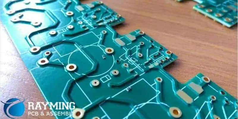
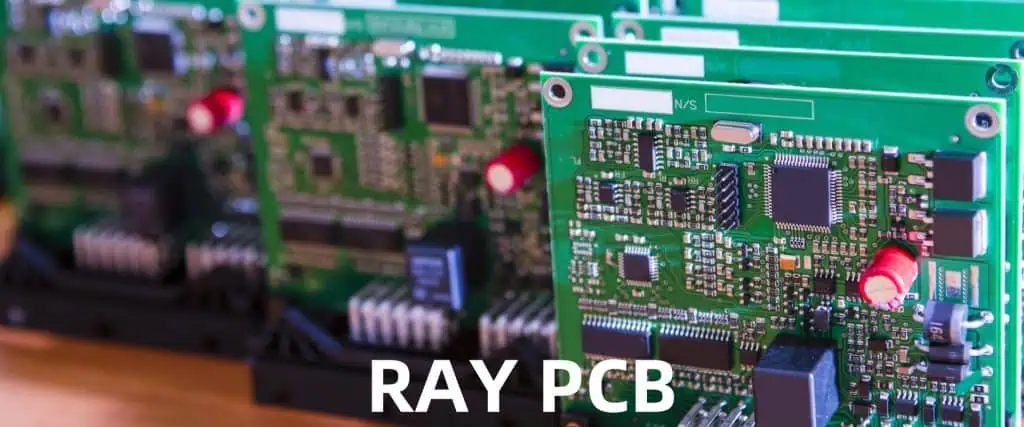
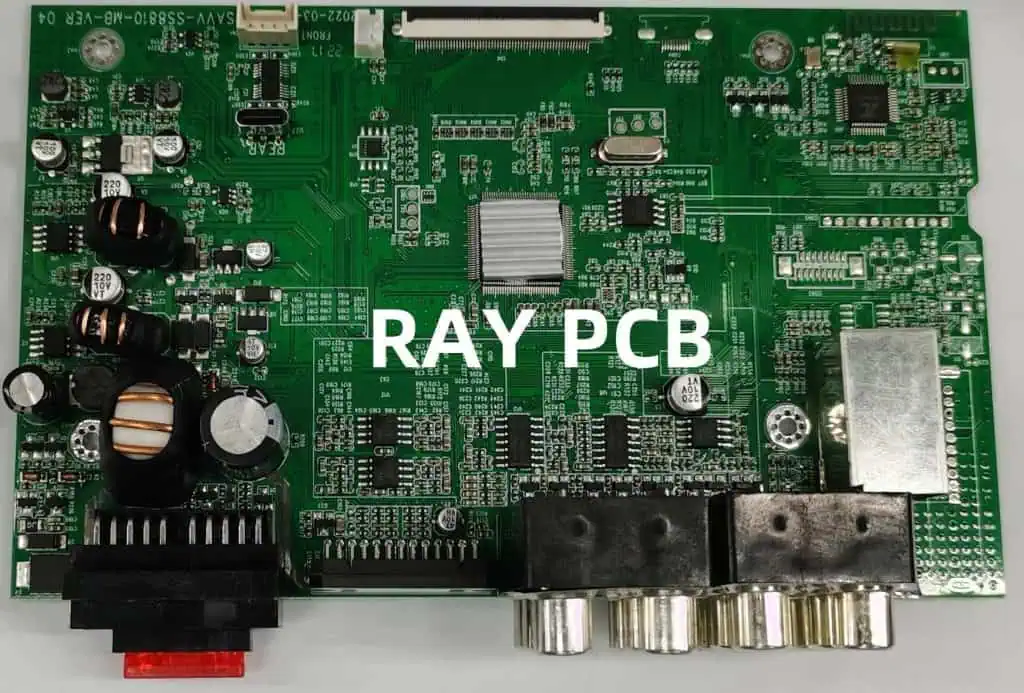
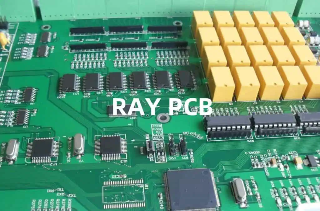
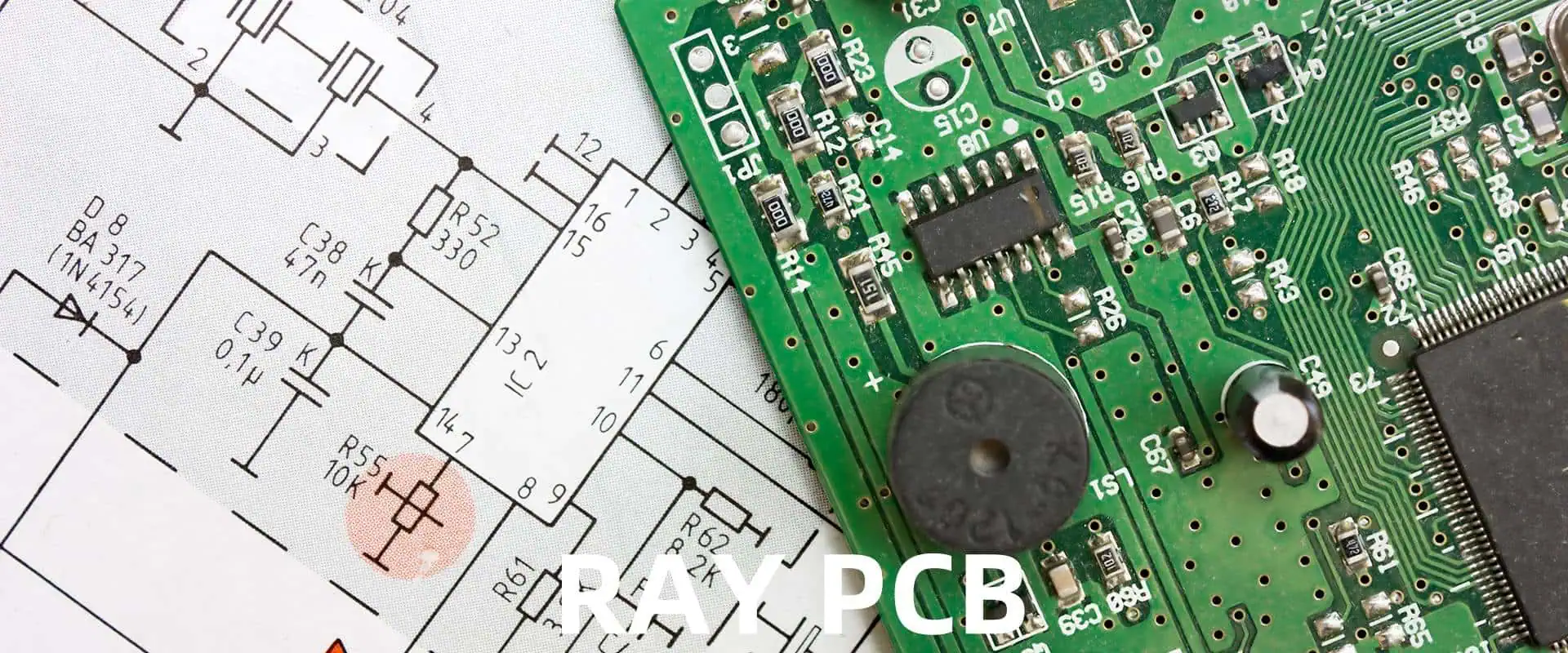
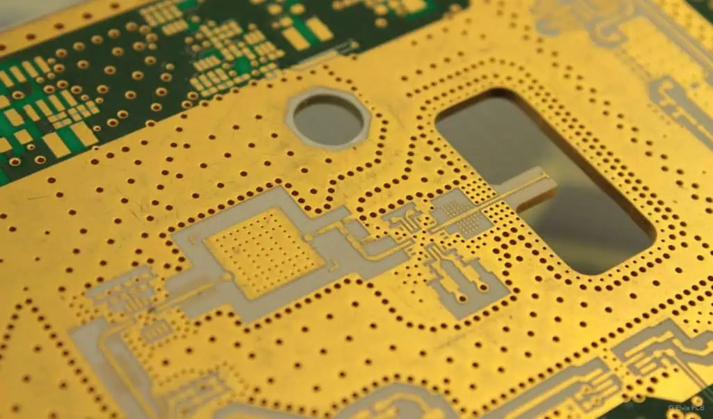
Copper roughness, also known as surface roughness, refers to the microscopic irregularities or deviations from a perfectly smooth surface on the copper traces and planes of a PCB. These irregularities can arise from various factors during the PCB manufacturing process, such as etching, plating, and lamination techniques.

Copper roughness is typically expressed in terms of roughness parameters, such as the root mean square (RMS) roughness or the peak-to-valley height. These parameters quantify the magnitude of the surface irregularities and provide a way to compare and specify the roughness levels of different PCBs.

Causes of Copper Roughness

Several factors can contribute to the roughness of the copper surface on PCBs, including:

  1. Etching Process: The etching process used to remove unwanted copper from the PCB’s substrate can leave behind microscopic irregularities on the remaining copper surfaces. The type of etchant, etching duration, and the etching technique employed can influence the resulting copper roughness.
  2. Electroplating: Electroplating is a common process used to deposit copper onto the PCB’s substrate. The plating parameters, such as current density, bath chemistry, and additives, can impact the smoothness of the deposited copper layer.
  3. Lamination Process: During the lamination process, the copper foil is bonded to the PCB’s dielectric substrate. The adhesion promotion techniques used, as well as the quality of the copper foil itself, can contribute to the overall copper roughness.
  4. Surface Treatments: Various surface treatments, such as oxidation or reduction processes, may be applied to the copper surfaces to improve adhesion or modify their properties. These treatments can potentially affect the smoothness of the copper surface.

Measuring Copper Roughness

To characterize and quantify copper roughness, several measurement techniques are employed in the PCB industry. These techniques include:

  1. Profilometry: Profilometry techniques, such as stylus profilometry or optical profilometry, directly measure the surface profile of the copper traces or planes. These techniques provide detailed information about the roughness parameters and can generate 2D or 3D surface profiles.
  2. Microscopy: Scanning electron microscopy (SEM) or atomic force microscopy (AFM) can be used to capture high-resolution images of the copper surface, allowing for visual inspection and analysis of the roughness features.
  3. Electrical Measurement: Certain electrical measurement techniques, such as the transmission line pulse (TLP) method or the line-roughness measurement (LRM) technique, can indirectly assess copper roughness by analyzing the electrical characteristics of the PCB traces or planes.

The choice of measurement technique depends on factors such as the required accuracy, measurement scale, and available equipment. Accurate measurement and characterization of copper roughness are essential for understanding its impact on signal integrity and developing strategies to mitigate its effects.

Effect of Copper Roughness on Signal Integrity

Copper roughness can have significant consequences for signal integrity in high-speed and high-frequency electronic systems. The key effects of copper roughness include:

1. Increased Signal Attenuation

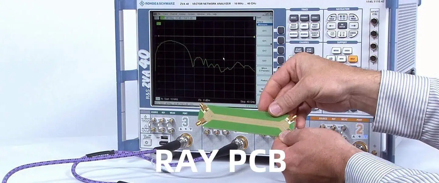
Roughness on the copper surface can cause additional signal losses due to increased skin effect and surface scattering. As the signal frequency increases, these losses become more pronounced, leading to higher signal attenuation and reduced transmission distances.

2. Impedance Discontinuities

Variations in the copper roughness along a transmission line can create localized changes in the effective cross-sectional area of the conductor, leading to impedance discontinuities. These discontinuities can cause signal reflections, ringing, and increased crosstalk, degrading signal quality.

3. Mode Conversion and Radiation

In differential signaling systems, copper roughness can cause mode conversion, where energy from the differential mode is converted into the common mode or vice versa. This mode conversion can lead to increased electromagnetic interference (EMI) and radiation, affecting signal integrity and potentially violating regulatory compliance.

4. Increased Insertion Loss

The increased surface area resulting from copper roughness can lead to higher capacitive and inductive losses, contributing to increased insertion loss in high-frequency signals. This effect becomes more significant as the operating frequency increases.

5. Jitter and Timing Errors

In high-speed digital systems, copper roughness can contribute to increased jitter and timing errors, potentially causing data corruption or system failures. These effects are particularly critical in applications such as high-speed serial links and clock distribution networks.

To mitigate the impact of copper roughness on signal integrity, various strategies can be employed, including optimizing the PCB fabrication processes, selecting appropriate surface finishes, incorporating roughness-aware design rules, and implementing equalization techniques in the signaling systems.

Strategies for Mitigating the Effects of Copper Roughness

While copper roughness is an inherent characteristic of PCB manufacturing processes, several strategies can be employed to mitigate its impact on signal integrity:

1. Optimized Fabrication Processes

Manufacturers can optimize their PCB fabrication processes to minimize copper roughness. This may involve adjusting etching parameters, employing advanced electroplating techniques, or using specialized surface treatments to achieve smoother copper surfaces.

2. Surface Finishes

Applying appropriate surface finishes, such as electroless nickel-immersion gold (ENIG) or immersion silver (ImAg), can help reduce the effective roughness of the copper surface by providing a smoother outer layer.

3. Roughness-Aware Design Rules

PCB designers can incorporate roughness-aware design rules into their layouts, taking into account the expected copper roughness levels. These rules may include adjustments to trace widths, spacing, and impedance calculations to compensate for the effects of roughness.

4. Equalization and Signal Processing

In high-speed digital systems, equalization techniques, such as transmitter pre-emphasis, receiver equalization, or continuous-time linear equalization (CTLE), can be employed to mitigate the effects of copper roughness on signal quality.

5. Material Selection

Careful selection of PCB materials, such as low-loss dielectric substrates and smoother copper foils, can help minimize the inherent roughness and its impact on signal integrity.

6. Design Validation and Modeling

Incorporating copper roughness models into signal integrity simulations and performing thorough design validation can help identify potential issues early in the design cycle and guide the implementation of appropriate mitigation strategies.

By adopting a combination of these strategies, electronics manufacturers and PCB designers can effectively manage the effects of copper roughness and ensure reliable signal integrity in their high-speed and high-frequency electronic systems.

Copper Roughness and Industry Standards

To ensure consistent and reliable performance of electronic systems, various industry standards and specifications have been established to address copper roughness. These standards provide guidelines, measurement techniques, and roughness limits for different applications and frequency ranges.

Some of the commonly referenced standards related to copper roughness include:

  • IPC-A-600 “Acceptability of Printed Boards”
  • IPC-6012 “Qualification and Performance Specification for Rigid Printed Boards”
  • IPC-6018 “Qualification and Performance Specification for High-Speed/High-Frequency Rigid Printed Board Laminates”
  • IEEE 802.3 Ethernet standards (e.g., 802.3ck for 100 Gb/s Ethernet)

These standards provide valuable guidance for PCB manufacturers, designers, and system integrators, helping them ensure compliance and maintain signal integrity in their products.

Frequently Asked Questions (FAQ)

  1. What is copper roughness, and why is it important? Copper roughness refers to the microscopic irregularities or deviations from a perfectly smooth surface on the copper traces and planes of a PCB. It is important because it can significantly impact signal integrity, especially in high-speed and high-frequency electronic systems, by causing signal attenuation, impedance discontinuities, mode conversion, and increased insertion loss.
  2. What are the main causes of copper roughness? The main causes of copper roughness include the etching process, electroplating techniques, lamination process, and surface treatments applied during PCB manufacturing.
  3. How is copper roughness measured? Copper roughness is typically measured using techniques such as profilometry (stylus or optical), microscopy (SEM or AFM), or electrical measurement methods like the transmission line pulse (TLP) or line-roughness

Mitigating Risk Factors for PCB Manufacturing Lead Times

In the fast-paced world of electronics manufacturing, time is of the essence. Ensuring timely delivery of printed circuit boards (PCBs) is crucial for maintaining efficient production schedules and meeting customer demands. However, various risk factors can contribute to extended lead times, causing delays and disruptions in the manufacturing process. This comprehensive article delves into the key risk factors associated with PCB manufacturing lead times and provides practical strategies to mitigate their impact.

Understanding PCB Manufacturing Lead Times

PCB manufacturing lead time refers to the duration between the placement of an order and the delivery of the finished PCBs. This timeframe encompasses several stages, including design review, prototyping, fabrication, assembly, testing, and shipping. Numerous factors can influence the lead time, ranging from design complexity to supply chain disruptions.

Common Risk Factors for Extended Lead Times

Several risk factors can contribute to extended PCB manufacturing lead times, including:

  1. Design Complexity: Intricate PCB designs with high component densities, complex routing, and multiple layers often require more time for fabrication and assembly.
  2. Supply Chain Disruptions: Shortages of critical components, raw materials, or equipment can cause delays in the manufacturing process.
  3. Quality Issues: Defects or non-conformities identified during testing or inspection may necessitate rework or even a complete restart of the manufacturing process, leading to longer lead times.
  4. Capacity Constraints: High demand for PCB manufacturing services can strain production capacities, resulting in longer queues and extended lead times.
  5. Geographical Distance: The physical distance between the PCB manufacturer and the customer can impact lead times due to transportation and logistics challenges.
  6. Regulatory Compliance: Adherence to industry-specific regulations and standards may require additional testing and documentation, potentially prolonging lead times.

Mitigating Risk Factors for PCB Manufacturing Lead Times

PCB solder mask expose machine

To effectively address the risk factors and minimize the impact on lead times, a comprehensive approach is necessary. The following strategies can be employed to mitigate the risks associated with PCB manufacturing lead times:

1. Design for Manufacturability (DFM)

Implementing Design for Manufacturability (DFM) principles during the PCB design stage can significantly reduce the risk of extended lead times. DFM practices involve optimizing the design to simplify the manufacturing process, minimize complexity, and ensure compliance with manufacturing guidelines. This approach includes:

  • Adhering to design rules and constraints provided by the PCB manufacturer
  • Minimizing complex routing and via structures
  • Utilizing standard component footprints and packages
  • Incorporating design verification and validation checks

By following DFM principles, potential manufacturing issues can be identified and addressed early in the design phase, reducing the need for rework and minimizing delays.

2. Supply Chain Management and Component Availability

Effective supply chain management is crucial for mitigating the risk of component shortages and delays. Strategies to improve supply chain resilience include:

  • Maintaining a diverse and reliable network of suppliers
  • Implementing inventory management systems for critical components
  • Monitoring and forecasting component demand and lead times
  • Exploring alternative component sources or substitutions when necessary

Additionally, considering component availability during the design phase and selecting readily available components can help minimize supply chain-related delays.

3. Quality Control and Testing

Implementing robust quality control measures throughout the manufacturing process can help identify and address potential issues early on, preventing rework and minimizing lead time impacts. Key quality control practices include:

  • Establishing clear acceptance criteria and testing procedures
  • Conducting in-process inspections and testing at various stages
  • Implementing statistical process control (SPC) and other quality monitoring techniques
  • Maintaining detailed documentation and traceability for quality records

By proactively addressing quality issues, rework and delays can be minimized, ensuring a smoother manufacturing process and faster lead times.

4. Capacity Planning and Production Scheduling

Effective capacity planning and production scheduling can help manage manufacturing workloads and ensure timely delivery of PCBs. Strategies to improve capacity management include:

  • Forecasting demand and production requirements
  • Investing in additional manufacturing capacity or equipment when necessary
  • Implementing lean manufacturing principles to optimize production flows
  • Collaborating with PCB manufacturers to align production schedules and priorities

By accurately forecasting demand and aligning production capacities, manufacturers can minimize bottlenecks and ensure a consistent flow of PCB production, reducing lead time variability.

5. Geographic Proximity and Logistics Optimization

Considering the geographic proximity of PCB manufacturers and optimizing logistics can help mitigate lead time risks associated with transportation and shipping. Strategies to address this factor include:

  • Selecting PCB manufacturers located closer to the end-user or assembly facilities
  • Implementing just-in-time (JIT) delivery strategies to minimize inventory levels
  • Optimizing shipping routes and modes of transportation
  • Leveraging advanced logistics technologies, such as real-time tracking and predictive analytics

By minimizing transportation distances and optimizing logistics processes, manufacturers can reduce shipping times and potential delays, ensuring timely delivery of PCBs.

6. Regulatory Compliance and Documentation

Adhering to industry-specific regulations and standards is essential for ensuring product quality and compliance. However, the associated documentation and testing requirements can contribute to extended lead times. To mitigate this risk, manufacturers should:

  • Stay up-to-date with relevant regulations and standards
  • Streamline documentation processes and leverage digital tools
  • Implement compliance checks early in the design and manufacturing stages
  • Collaborate with PCB manufacturers and regulatory bodies for guidance and best practices

By proactively addressing regulatory requirements and optimizing documentation processes, manufacturers can minimize delays associated with compliance-related activities.

Monitoring and Continuous Improvement

Mitigating risk factors for PCB manufacturing lead times is an ongoing process that requires continuous monitoring and improvement. Manufacturers should regularly review and analyze lead time data, identify recurring issues or bottlenecks, and implement corrective actions to address them. Additionally, fostering open communication and collaboration with PCB manufacturers, suppliers, and customers can facilitate the sharing of best practices and facilitate continuous improvement efforts.

Frequently Asked Questions (FAQ)

  1. What is the impact of extended PCB manufacturing lead times? Extended PCB manufacturing lead times can result in production delays, missed delivery deadlines, and potential revenue losses. They can also disrupt the overall supply chain and impact customer satisfaction.
  2. How can Design for Manufacturability (DFM) principles help mitigate lead time risks? DFM principles help optimize the PCB design for the manufacturing process, reducing complexity and potential issues that could cause delays or rework. By addressing manufacturability concerns early in the design phase, lead times can be minimized.
  3. What role does supply chain management play in mitigating lead time risks? Effective supply chain management is crucial for ensuring the availability of components and materials required for PCB manufacturing. By maintaining a diverse supplier network, implementing inventory management systems, and monitoring component lead times, manufacturers can minimize delays caused by supply chain disruptions.
  4. How can quality control and testing practices contribute to reducing PCB manufacturing lead times? Robust quality control and testing practices allow for early identification and resolution of potential issues, preventing rework and minimizing delays. In-process inspections, statistical process control, and detailed documentation can help streamline the manufacturing process and reduce lead times.
  5. What strategies can be employed to address capacity constraints and production scheduling challenges? Strategies such as forecasting demand, investing in additional manufacturing capacity, implementing lean manufacturing principles, and collaborating with PCB manufacturers on production scheduling can help manage workloads and ensure timely delivery of PCBs.

Conclusion

Mitigating risk factors for PCB manufacturing lead times is a multifaceted endeavor that requires a holistic approach. By implementing Design for Manufacturability principles, maintaining effective supply chain management, implementing robust quality control measures, optimizing capacity planning and production scheduling, considering geographic proximity and logistics optimization, and adhering to regulatory compliance requirements, manufacturers can significantly reduce the impact of lead time risks.

Continuous monitoring, data analysis, and collaboration with stakeholders are essential for identifying and addressing emerging risks and implementing corrective actions. By proactively managing these risk factors, manufacturers can ensure timely delivery of PCBs, maintain efficient production schedules, and enhance customer satisfaction.

Remember, lead time management is an ongoing process that requires vigilance, adaptation, and a commitment to continuous improvement. By embracing these strategies and fostering a culture of risk mitigation, manufacturers can stay ahead of the curve and maintain a competitive edge in the dynamic world of PCB manufacturing.

EMC on the Board and Off the Board You Need Know

pcb emi

Electromagnetic compatibility (EMC) is a crucial aspect of electronic product design and development. It ensures that electronic devices can operate without causing or experiencing unacceptable levels of electromagnetic interference (EMI). EMC is not just a single concept; it encompasses a wide range of principles, regulations, and best practices that must be adhered to throughout the entire product lifecycle, from design to manufacturing and operation.

In this comprehensive article, we will delve into the intricacies of EMC, exploring its significance, underlying principles, and practical implementation strategies. Whether you’re an engineer, a product manager, or simply someone interested in understanding the complexities of modern electronics, this article will provide valuable insights into the world of EMC.

Understanding EMC

EMC is a multifaceted discipline that encompasses three main aspects: emissions, immunity, and safety. Each of these aspects plays a vital role in ensuring the proper functioning of electronic devices and systems.

Emissions

Emissions refer to the electromagnetic energy radiated or conducted by an electronic device. This energy can potentially interfere with the operation of other devices or systems in the vicinity. EMC regulations and standards set limits on the amount of emissions that a device can produce, to ensure that it does not cause harmful interference.

Immunity

Immunity is the ability of an electronic device or system to function properly in the presence of electromagnetic interference (EMI) from external sources. EMI can originate from various sources, such as nearby electronic devices, power lines, or even natural phenomena like lightning. EMC standards and guidelines outline the required immunity levels for different types of devices and environments.

Safety

EMC also plays a crucial role in ensuring the safety of electronic devices and systems. Excessive electromagnetic fields can pose potential risks to human health and the environment. EMC regulations and standards aim to limit exposure to these fields, ensuring that electronic products are safe for use in their intended environments.

EMC in Product Design

Incorporating EMC principles into product design is essential for ensuring compliance with relevant regulations and standards, as well as ensuring the proper functioning and reliability of electronic devices. Here are some key considerations and best practices for EMC in product design:

PCB Layout and Component Placement

The layout of the printed circuit board (PCB) and the placement of components can significantly impact EMC performance. Proper PCB design practices, such as separating analog and digital circuits, using ground planes, and implementing EMI shielding techniques, can help mitigate EMI issues.

Shielding and Grounding

Effective shielding and grounding strategies are crucial for EMC compliance. Shielding involves enclosing sensitive components or entire devices within conductive materials to prevent EMI from entering or leaving the system. Proper grounding techniques ensure that unwanted currents and signals have a low-impedance path to ground, reducing the risk of EMI.

Cable and Connector Design

Cables and connectors can act as antennas, radiating or receiving EMI. Careful design and selection of cables and connectors, including the use of shielded cables and filtered connectors, can help mitigate EMI issues.

Software and Firmware Considerations

While EMC is often associated with hardware design, software and firmware can also play a role in EMC performance. Proper software design practices, such as implementing noise filtering algorithms and avoiding high-frequency switching or clock signals, can contribute to improved EMC performance.

EMC Testing and Compliance

EMC testing is an essential part of the product development process, ensuring that electronic devices and systems comply with relevant regulations and standards. There are various types of EMC tests, each designed to evaluate specific aspects of EMC performance.

Emissions Testing

Emissions testing measures the electromagnetic energy radiated or conducted by a device. Common emissions tests include:

  • Radiated emissions testing
  • Conducted emissions testing
  • Harmonic and flicker testing

Immunity Testing

Immunity testing evaluates the ability of a device or system to function properly in the presence of EMI. Common immunity tests include:

Pre-compliance and Full-compliance Testing

Pre-compliance testing is often performed early in the product development cycle to identify potential EMC issues and guide design improvements. Full-compliance testing is typically conducted at a certified testing laboratory to obtain formal certification or approval for a product.

EMC Regulations and Standards

EMC is governed by a variety of regulations and standards, which vary depending on the product type, intended use, and geographical region. Some of the most widely recognized EMC standards include:

  • IEC 61000 series (International Electrotechnical Commission)
  • CISPR (Comitรฉ International Spรฉcial des Perturbations Radioรฉlectriques)
  • FCC Part 15 (Federal Communications Commission, United States)
  • VCCI (Voluntary Control Council for Interference, Japan)
  • EN 55022/55024 (European Union)

Compliance with these standards is often mandatory for electronic products sold in various markets, and failure to meet EMC requirements can result in fines, product recalls, or even legal liabilities.

EMC Best Practices

Achieving EMC compliance and ensuring the proper functioning of electronic devices requires adhering to best practices throughout the product development lifecycle. Here are some key EMC best practices:

Design Reviews and Simulations

Conducting regular design reviews and performing EMC simulations can help identify potential EMC issues early in the design process, enabling timely corrections and optimizations.

Proper Documentation and Revision Control

Maintaining thorough documentation and implementing robust revision control practices are essential for tracking design changes, test results, and compliance efforts throughout the product lifecycle.

Training and Awareness

Providing EMC training and promoting awareness among engineers, designers, and other stakeholders can help foster a culture of EMC compliance and ensure that EMC considerations are integrated into all aspects of product development.

Continuous Improvement and Monitoring

EMC is an ongoing process, and it is crucial to continuously monitor and improve EMC performance, even after a product has been released to the market. This includes tracking customer feedback, industry trends, and regulatory updates, and making necessary adjustments to maintain compliance and product quality.

Frequently Asked Questions (FAQ)

  1. Why is EMC important? EMC is crucial for ensuring the proper functioning of electronic devices and systems, preventing harmful interference, and ensuring safety. Failure to address EMC considerations can lead to product malfunctions, regulatory non-compliance, and potential safety risks.
  2. What is the difference between emissions and immunity in EMC? Emissions refer to the electromagnetic energy radiated or conducted by a device, while immunity is the ability of a device or system to function properly in the presence of external electromagnetic interference (EMI).
  3. Can software and firmware impact EMC performance? Yes, software and firmware can influence EMC performance. Proper software design practices, such as implementing noise filtering algorithms and avoiding high-frequency switching or clock signals, can contribute to improved EMC performance.
  4. What are the consequences of non-compliance with EMC regulations? Non-compliance with EMC regulations can result in fines, product recalls, legal liabilities, and potential damage to a company’s reputation and customer trust.
  5. How often should EMC testing be performed? EMC testing should be performed throughout the product development lifecycle, including pre-compliance testing early in the design phase and full-compliance testing before product release. Ongoing monitoring and testing may also be necessary to ensure continued compliance and product quality.

Conclusion

EMC is a critical aspect of electronic product design and development, ensuring the proper functioning of devices, preventing harmful interference, and maintaining safety standards. By understanding the principles of EMC, incorporating best practices into product design, and adhering to relevant regulations and standards, manufacturers can create high-quality, reliable, and compliant electronic products.

As technology continues to evolve and electronic devices become more complex and interconnected, the importance of EMC will only continue to grow. Staying up-to-date with industry trends, regulatory changes, and emerging best practices will be essential for maintaining a competitive edge and delivering products that meet the highest standards of performance and quality.

Remember, EMC is not just a box to check; it is an ongoing commitment to excellence, safety, and responsible product development.

Why Start-ups or Small Businesses Should Choose Full Turnkey PCB Assembly?

In today’s fast-paced and competitive business landscape, start-ups and small businesses face numerous challenges when it comes to bringing their electronic products to market. From limited resources and budgets to lack of expertise and manufacturing capabilities, these companies often struggle to navigate the complex process of printed circuit board (PCB) assembly. This is where full turnkey PCB assembly services come into play, offering a comprehensive and streamlined solution that can significantly benefit start-ups and small businesses. In this article, we will explore the reasons why these companies should consider full turnkey PCB assembly and how it can contribute to their success.

Understanding Full Turnkey PCB Assembly

What is Full Turnkey PCB Assembly?

Full turnkey PCB assembly is a comprehensive service that encompasses the entire process of transforming a PCB design into a fully assembled and tested electronic product. It involves a range of services, including:

With full turnkey PCB assembly, companies can leverage the expertise and resources of a specialized service provider, allowing them to focus on their core competencies while ensuring that their electronic products are manufactured to the highest standards.

Benefits of Full Turnkey PCB Assembly for Start-ups and Small Businesses

  1. Cost Savings: By outsourcing the entire PCB assembly process, start-ups and small businesses can avoid the substantial upfront investments required for establishing their own manufacturing facilities, equipment, and skilled workforce. This can lead to significant cost savings, especially in the early stages of product development and small-scale production runs.
  2. Access to Expertise and Advanced Technologies: Full turnkey PCB assembly providers possess extensive experience and expertise in PCB manufacturing, assembly, and testing processes. They also have access to state-of-the-art equipment and technologies, ensuring that products are assembled with precision and quality control measures in place.
  3. Scalability and Flexibility: As start-ups and small businesses grow, their production needs may fluctuate. Full turnkey PCB assembly services offer scalability and flexibility, allowing companies to adjust their production volumes according to market demand without the burden of managing additional resources or infrastructure.
  4. Reduced Time-to-Market: With a streamlined and efficient assembly process, full turnkey PCB assembly services can significantly reduce the time required to bring products to market. This can be a crucial advantage in highly competitive markets where being first to market can provide a significant edge.
  5. Quality Assurance and Compliance: Reputable full turnkey PCB assembly providers adhere to strict quality control procedures and industry standards, ensuring that the assembled products meet the required specifications and regulatory compliance requirements.

Choosing the Right Full Turnkey PCB Assembly Provider

When selecting a full turnkey PCB assembly provider, start-ups and small businesses should consider the following factors:

  1. Experience and Expertise: Look for a provider with a proven track record in PCB assembly and a deep understanding of the latest technologies and industry best practices.
  2. Manufacturing Capabilities: Evaluate the provider’s manufacturing capabilities, including their equipment, facilities, and ability to handle various PCB complexities and production volumes.
  3. Quality Control and Certifications: Ensure that the provider has robust quality control processes in place and holds relevant certifications, such as ISO 9001, to guarantee consistent quality and compliance.
  4. Component Sourcing and Supply Chain Management: Inquire about the provider’s component sourcing capabilities, including their relationships with suppliers and their ability to manage the supply chain effectively.
  5. Communication and Support: Effective communication and responsive support are crucial for successful collaboration. Look for a provider that values open communication, provides regular updates, and offers dedicated support throughout the assembly process.
  6. Pricing and Turnaround Times: While cost is an important consideration, it should not be the sole deciding factor. Evaluate the provider’s pricing structure, turnaround times, and overall value proposition.
  7. Intellectual Property Protection: For start-ups and small businesses with innovative products, it is essential to ensure that the provider has measures in place to protect intellectual property and maintain confidentiality.

Advantages of Full Turnkey PCB Assembly for Start-ups and Small Businesses

1. Focus on Core Competencies

By outsourcing the PCB assembly process, start-ups and small businesses can concentrate their efforts and resources on their core competencies, such as product design, marketing, and business development. This allows them to allocate their limited resources more effectively and maintain a competitive edge in their respective markets.

2. Reduced Overhead and Capital Investments

Establishing an in-house PCB assembly line requires substantial capital investments in equipment, facilities, and skilled personnel. Full turnkey PCB assembly services eliminate these upfront costs, freeing up valuable resources that can be reinvested in other areas of the business.

3. Access to Advanced Technologies and Expertise

Full turnkey PCB assembly providers invest in the latest equipment, technologies, and skilled personnel to stay competitive and meet the evolving demands of the industry. By leveraging these resources, start-ups and small businesses can benefit from advanced manufacturing capabilities without the need for significant investments.

4. Improved Time-to-Market

Time-to-market is a critical factor in the success of electronic products, especially in highly competitive markets. Full turnkey PCB assembly services can significantly accelerate the manufacturing process, enabling start-ups and small businesses to bring their products to market faster and capitalize on emerging opportunities.

5. Scalability and Flexibility

As a start-up or small business grows, its production needs may fluctuate. Full turnkey PCB assembly services offer the flexibility to scale production up or down based on demand, without the need for additional investments in infrastructure or personnel.

6. Quality Assurance and Compliance

Reputable full turnkey PCB assembly providers adhere to strict quality control protocols and industry standards, ensuring that the assembled products meet the required specifications and regulatory compliance requirements. This can provide peace of mind to start-ups and small businesses, allowing them to focus on other aspects of their operations.

7. Supply Chain Management

Sourcing and managing the supply chain for PCB components can be a complex and time-consuming task, especially for start-ups and small businesses with limited resources. Full turnkey PCB assembly providers have established relationships with suppliers and robust supply chain management systems, ensuring timely and reliable component procurement.

Potential Challenges and Considerations

While full turnkey PCB assembly offers numerous benefits for start-ups and small businesses, there are some potential challenges and considerations to keep in mind:

  1. Intellectual Property Protection: When outsourcing PCB assembly, it is essential to ensure that the provider has robust measures in place to protect intellectual property and maintain confidentiality. This may include non-disclosure agreements (NDAs) and secure data transfer protocols.
  2. Communication and Collaboration: Effective communication and collaboration between the start-up/small business and the full turnkey PCB assembly provider are crucial for successful project execution. It is important to establish clear communication channels and processes to ensure alignment and address any issues or concerns promptly.
  3. Quality Control and Oversight: While full turnkey PCB assembly providers have quality control measures in place, start-ups and small businesses should consider implementing their own quality control processes, such as sample inspections or on-site audits, to ensure that their products meet the required specifications.
  4. Lead Times and Logistics: Depending on the location of the full turnkey PCB assembly provider and the complexity of the product, lead times and logistics can be a consideration. It is essential to factor in shipping times, customs clearance, and any potential delays to ensure timely delivery of the assembled products.

To mitigate these potential challenges, it is recommended to thoroughly evaluate and select a reputable full turnkey PCB assembly provider that meets the specific needs and requirements of the start-up or small business.

FQA (Frequently Asked Questions)

  1. What is the difference between full turnkey PCB assembly and partial assembly services? Full turnkey PCB assembly encompasses the entire process from PCB fabrication to final assembly and testing, providing a complete end-to-end solution. Partial assembly services, on the other hand, only cover specific stages of the assembly process, such as component placement or soldering.
  2. How does full turnkey PCB assembly contribute to cost savings for start-ups and small businesses? Full turnkey PCB assembly services eliminate the need for substantial upfront investments in manufacturing facilities, equipment, and skilled personnel. By outsourcing the entire assembly process, start-ups and small businesses can significantly reduce their overhead costs, especially during the early stages of product development and small-scale production runs.
  3. What are the typical quality control measures implemented by full turnkey PCB assembly providers? Reputable full turnkey PCB assembly providers employ various quality control measures, including automated optical inspection (AOI), in-circuit testing (ICT), functional testing, and adherence to industry standards and certifications like ISO 9001. These measures ensure that the assembled products meet the

3D Printing Circuit Boards for Fast Prototyping

3D Print PCB

In the ever-evolving world of electronics and product development, rapid prototyping has become a crucial aspect of the design process. Traditional methods of creating printed circuit boards (PCBs) can be time-consuming and costly, particularly in the early stages of development. However, with the advent of 3D printing technology, a new era of fast and efficient prototyping has emerged. 3D printing circuit boards offer a revolutionary approach to prototyping, enabling designers and engineers to quickly iterate and test their designs before committing to full-scale production.

The Benefits of 3D Printing Circuit Boards

1. Rapid Prototyping

One of the most significant advantages of 3D printing circuit boards is the speed at which prototypes can be produced. Unlike traditional PCB manufacturing processes, which can take weeks or even months, 3D printing allows for the creation of functional prototypes within hours or days. This accelerated timeline enables designers and engineers to quickly test and validate their designs, identify potential issues, and make necessary modifications before proceeding to the next stage of development.

2. Cost-Effective Prototyping

Traditional PCB prototyping methods often involve significant upfront costs, including tooling and setup fees. 3D printing circuit boards, on the other hand, eliminates many of these costs, making prototyping more accessible and cost-effective, especially for small-scale projects or initial design iterations. By reducing the financial barriers to prototyping, 3D printing encourages more experimentation and innovation.

3. Design Flexibility

3D printing technology offers unparalleled design flexibility when it comes to creating circuit boards. Unlike traditional manufacturing methods, which are constrained by the limitations of subtractive processes (e.g., etching), 3D printing allows for the creation of complex geometries and freeform shapes. This flexibility enables designers to explore unique form factors, integrate novel features, and push the boundaries of PCB design.

4. Reduced Lead Times

Traditional PCB manufacturing processes often involve multiple steps, including design, fabrication, assembly, and testing, each with its own lead time. 3D printing circuit boards streamlines this process by consolidating several steps into a single operation. By reducing the number of separate processes and eliminating the need for specialized tooling, 3D printing significantly reduces overall lead times, allowing for faster iterations and a more agile development cycle.

3D Printing Technologies for Circuit Boards

Several 3D printing technologies have been adapted for the fabrication of circuit boards, each with its own advantages and limitations. Here are some of the most commonly used methods:

1. Fused Deposition Modeling (FDM)

Fused Deposition Modeling (FDM) is one of the most widely used 3D printing technologies for circuit board prototyping. In this process, a thermoplastic material, such as polylactic acid (PLA) or acrylonitrile butadiene styrene (ABS), is heated and extruded through a nozzle onto a build platform, creating the desired structure layer by layer.

FDM is particularly well-suited for prototyping due to its affordability, ease of use, and the availability of a wide range of conductive and dielectric materials. However, it is generally limited in terms of resolution and accuracy compared to other 3D printing methods.

2. Stereolithography (SLA)

Stereolithography (SLA) is a 3D printing technology that utilizes a photopolymer resin and a UV laser to selectively cure and solidify the resin layer by layer. This process allows for the creation of highly detailed and accurate circuit board prototypes with excellent resolution and surface finish.

While SLA offers superior quality compared to FDM, it is generally more expensive and requires specialized materials and post-processing steps. Additionally, the range of available conductive materials for SLA is currently more limited than FDM.

3. Direct Ink Writing (DIW)

Direct Ink Writing (DIW), also known as robotic deposition or paste extrusion, is a 3D printing technique that involves the extrusion of conductive and dielectric inks or pastes through a nozzle onto a substrate. This method enables the direct fabrication of multi-material and multi-functional circuit boards with embedded components and interconnects.

DIW offers the ability to create complex geometries and integrate various functional materials, such as conductive traces, resistors, capacitors, and sensors, within a single printing process. However, it requires specialized equipment and materials, and the resolution and accuracy may be lower compared to other 3D printing methods.

4. Aerosol Jet Printing

Aerosol Jet Printing is a maskless, non-contact printing technique that utilizes an aerosol of conductive or dielectric inks to create circuit board patterns and components. This method offers high resolution and the ability to print on a wide range of substrates, including flexible and non-planar surfaces.

Aerosol Jet Printing is particularly well-suited for creating highly customized and specialized circuit boards, such as those used in wearable electronics, Internet of Things (IoT) devices, and flexible electronics applications.

Materials for 3D Printed Circuit Boards

The choice of materials is crucial in the fabrication of 3D printed circuit boards. These materials must possess specific properties to ensure conductivity, insulation, and overall functionality. Here are some of the commonly used materials:

1. Conductive Materials

  • Conductive thermoplastics: These materials incorporate conductive fillers, such as carbon black, carbon nanotubes, or metal particles, into a thermoplastic matrix, enabling the creation of conductive traces and interconnects.
  • Conductive inks and pastes: These are specialized formulations containing conductive particles (e.g., silver, copper, or carbon) suspended in a carrier solvent or binder. They are used in DIW and Aerosol Jet Printing processes.
  • Metallic filaments: Filaments made from metals like copper or stainless steel can be used in FDM printing for creating conductive traces or structures.

2. Dielectric Materials

  • Thermoplastics (e.g., PLA, ABS, Nylon): These materials serve as insulating substrates and dielectric layers in 3D printed circuit boards.
  • Photopolymer resins: Used in SLA printing, these resins provide insulation and structural support for the circuit board.
  • Dielectric inks and pastes: Similar to conductive inks, dielectric inks and pastes are used in DIW and Aerosol Jet Printing to create insulating layers and encapsulate components.

3. Substrate Materials

  • Rigid substrates (e.g., FR-4, ceramic): These materials provide a stable base for mounting components and creating rigid circuit boards.
  • Flexible substrates (e.g., polyimide films, polyethylene terephthalate (PET)): Used for creating flexible and conformal circuit boards.

Design and Workflow Considerations

To effectively utilize 3D printing for circuit board prototyping, several design and workflow considerations must be taken into account:

1. Design Software and File Formats

Specialized design software and file formats are required for creating 3D printable circuit board designs. Popular software options include Eagle, KiCad, and Autodesk EAGLE, which support the generation of 3D models and export formats compatible with various 3D printing technologies.

2. Design Rules and Constraints

Each 3D printing technology has its own set of design rules and constraints, such as minimum feature sizes, layer thicknesses, and material compatibility. Designers must familiarize themselves with these rules and ensure that their designs adhere to the specific requirements of the chosen printing method.

3. Post-Processing and Assembly

Depending on the 3D printing technology and materials used, post-processing steps may be required to enhance conductivity, provide surface finishes, or enable component assembly. These steps can include curing, sintering, electroplating, or the application of conductive coatings.

4. Workflow Integration

To streamline the prototyping process, it is essential to integrate 3D printing into the overall product development workflow. This may involve establishing procedures for design review, test and evaluation, and feedback loops to incorporate any necessary modifications into subsequent iterations.

Applications of 3D Printed Circuit Boards

The versatility and rapid prototyping capabilities of 3D printed circuit boards have opened up a wide range of applications across various industries:

1. Electronics and Consumer Products

3D printed circuit boards are extensively used in the development of consumer electronics, wearable devices, and Internet of Things (IoT) products. The ability to quickly prototype and iterate designs allows for faster time-to-market and improved product development cycles.

2. Aerospace and Automotive

The aerospace and automotive industries benefit from the ability to create lightweight, customized, and conformal circuit boards using 3D printing. These industries often require unique form factors and integrated

Types of PCBs

Printed circuit boards (PCBs) are the backbone of modern electronics, providing a platform for mounting and interconnecting electronic components. These boards come in various types, each designed to cater to specific applications and requirements. In this comprehensive article, we will explore the different types of PCBs, their characteristics, and their applications.

Single-Sided PCBs

single layer pcb

Overview

Single-sided PCBs are the simplest and most basic type of printed circuit boards. As the name suggests, these boards have conductive patterns printed on one side of the insulating substrate material, typically a fiberglass-reinforced epoxy resin or a phenolic resin.

Characteristics

  • Cost-effective and suitable for low-density circuits
  • Components are mounted and soldered on one side of the board
  • Limited interconnection density due to the single layer of conductive patterns
  • Primarily used in simple electronic devices and prototyping

Applications

Double-Sided PCBs

Overview

Double-sided PCBs, also known as double-layer PCBs, have conductive patterns printed on both sides of the insulating substrate material. These boards offer increased interconnection density and component mounting capacity compared to single-sided PCBs.

Characteristics

  • Increased interconnection density and component mounting area
  • Conductive layers on both sides of the board are connected through plated-through holes or vias
  • Higher circuit complexity and functionality compared to single-sided PCBs
  • More expensive than single-sided PCBs due to additional manufacturing processes

Applications

  • Consumer electronics (e.g., mobile phones, digital cameras)
  • Industrial control systems
  • Automotive electronics
  • Medical devices

Multi-Layer PCBs

Overview

Multi-layer PCBs are advanced printed circuit boards that consist of multiple conductive layers separated by insulating material. These layers are interconnected through vias, allowing for intricate routing and high-density component placement.

Characteristics

  • High interconnection density and component mounting capacity
  • Consist of four or more conductive layers (typically ranging from 4 to 16 layers)
  • Increased complexity and manufacturing challenges compared to single and double-sided PCBs
  • Higher cost due to the additional layers and manufacturing processes

Types of Multi-Layer PCBs

Rigid PCBs

  • Rigid PCBs are made from sturdy materials like fiberglass-reinforced epoxy resin
  • Suitable for applications requiring robust and durable boards
  • Used in desktop computers, servers, and industrial equipment

Flexible PCBs

  • Flexible PCBs are made from flexible materials like polyimide or polyester films
  • Capable of bending and conforming to various shapes
  • Used in applications requiring flexibility, such as wearable electronics and flexible displays

Rigid-Flex PCBs

  • Rigid-Flex PCBs combine rigid and flexible sections in a single board
  • Offer the benefits of both rigid and flexible PCBs in one design
  • Used in applications requiring both rigidity and flexibility, such as aerospace and medical devices

Applications

  • High-performance computing systems
  • Telecommunications equipment
  • Aerospace and defense systems
  • Automotive electronics
  • Medical devices

High-Density Interconnect (HDI) PCBs

Overview

High-Density Interconnect (HDI) PCBs are a specialized type of multi-layer PCBs designed to accommodate an extremely high density of components and interconnections. These boards are characterized by their ability to pack a large number of components in a small area while maintaining signal integrity and reliability.

Characteristics

  • Micro-vias (blind or buried vias) with diameters as small as 0.1mm
  • High-density component mounting and fine-pitch ball grid array (BGA) packages
  • Laser-drilled micro-vias for precise interconnections
  • Advanced manufacturing techniques, such as sequential lamination and laser ablation

Applications

  • High-end mobile devices (e.g., smartphones, tablets)
  • Portable computing devices
  • High-performance networking equipment
  • Advanced medical devices
  • Aerospace and defense systems

Specialized PCBs

Overview

In addition to the standard PCB types, there are several specialized PCBs designed for specific applications or environments. These PCBs incorporate unique features or materials to meet specific requirements.

Types of Specialized PCBs

Heavy Copper PCBs

heavy copper pcb
  • Feature thicker copper layers (up to 6 oz/ftยฒ or more)
  • Designed to handle high current loads and dissipate heat effectively
  • Used in power supply units, motor controllers, and high-power applications

Aluminum-backed PCBs

  • Consist of a standard PCB bonded to an aluminum substrate
  • Provide excellent heat dissipation capabilities
  • Suitable for high-power electronics and LED lighting applications

RF and Microwave PCBs

Rogers AD255C PCB
  • Designed for radio frequency (RF) and microwave applications
  • Utilize low-loss dielectric materials and specialized interconnect structures
  • Used in wireless communication systems, radar systems, and satellite equipment

High-Temperature PCBs

  • Capable of withstanding extreme temperatures (up to 200ยฐC or higher)
  • Utilize specialized materials like polyimide or ceramic substrates
  • Used in aerospace, automotive, and industrial applications with high-temperature environments

Applications

  • Power electronics
  • LED lighting systems
  • Wireless communication equipment
  • Aerospace and defense systems
  • Automotive electronics
  • Industrial automation and control systems

FQA (Frequently Asked Questions)

  1. What is the difference between single-sided and double-sided PCBs? Single-sided PCBs have conductive patterns printed on one side of the insulating substrate, while double-sided PCBs have conductive patterns printed on both sides, allowing for increased interconnection density and component mounting capacity.
  2. What are the advantages of multi-layer PCBs? Multi-layer PCBs offer high interconnection density, component mounting capacity, and the ability to accommodate complex circuit designs. They are suitable for high-performance computing systems, telecommunications equipment, and aerospace and defense applications.
  3. What are HDI PCBs, and what are their applications? High-Density Interconnect (HDI) PCBs are specialized multi-layer PCBs designed to accommodate an extremely high density of components and interconnections. They are used in high-end mobile devices, portable computing devices, and advanced medical and aerospace systems.
  4. What are the benefits of flexible PCBs? Flexible PCBs are made from flexible materials like polyimide or polyester films, allowing them to bend and conform to various shapes. They are used in applications requiring flexibility, such as wearable electronics and flexible displays.
  5. What are some examples of specialized PCBs? Specialized PCBs include heavy copper PCBs for high-power applications, aluminum-backed PCBs for heat dissipation, RF and microwave PCBs for wireless communication systems, and high-temperature PCBs for extreme environments in aerospace and industrial applications.

Conclusion

Printed circuit boards come in various types, each designed to meet specific requirements and applications. From the basic single-sided PCBs to the advanced multi-layer and high-density interconnect PCBs, each type offers unique advantages and capabilities. Understanding the different types of PCBs is crucial for selecting the appropriate board for a given application, ensuring optimal performance, reliability, and cost-effectiveness. As electronic devices continue to evolve, the demand for specialized and innovative PCB designs will continue to grow, driving further advancements in this critical component of modern electronics.

How to choose the PCB Prototype Manufacturer for critical electronic device design?

In the ever-evolving world of electronics, the design and development of critical electronic devices demand meticulous attention to detail and a commitment to excellence. Prototyping plays a crucial role in this process, allowing engineers and designers to validate their concepts, identify potential issues, and refine their designs before moving into full-scale production. Choosing the right PCB (Printed Circuit Board) prototype manufacturer is a critical decision that can significantly impact the success of your project.

This comprehensive guide will explore the key factors to consider when selecting a PCB prototype assembly manufacturer for critical electronic device design, ensuring that your project stays on track, meets stringent quality standards, and ultimately delivers a high-performing and reliable product.

Understanding the Importance of PCB Prototyping

Validating Design Concepts

The prototyping phase is essential for validating design concepts and ensuring that the electronic device functions as intended. By creating a physical prototype, engineers and designers can test the performance, functionality, and integration of various components, identifying potential issues or areas for improvement before committing to full-scale production.

Identifying and Resolving Design Flaws Early

Prototyping allows for the early identification and resolution of design flaws, which can be costly and time-consuming to address at later stages of the product development cycle. By catching and addressing issues during the prototyping phase, manufacturers can save significant resources and minimize the risk of product recalls or failures.

Refining and Optimizing Designs

The prototyping process provides valuable insights and opportunities for refining and optimizing designs. Based on the feedback and data gathered from prototype testing, engineers and designers can make informed decisions and implement necessary adjustments, ensuring that the final product meets or exceeds performance requirements and user expectations.

Criteria for Selecting a PCB Prototype Manufacturer

Technical Capabilities and Expertise

When selecting a PCB prototype manufacturer for critical electronic device design, it is essential to consider their technical capabilities and expertise. Look for manufacturers with a proven track record in handling complex PCB designs, as well as experience working with the specific technologies and components involved in your project.

Evaluate their manufacturing processes, equipment, and personnel qualifications to ensure they have the necessary resources and expertise to deliver high-quality prototypes that accurately represent your intended design.

Quality Assurance and Compliance

Quality assurance and compliance are paramount considerations when dealing with critical electronic devices. Choose a PCB prototype manufacturer that adheres to strict quality control measures and follows industry-recognized standards and certifications, such as ISO 9001, IPC-A-600, and RoHS compliance.

Verify their testing and inspection processes, including automated optical inspection (AOI), flying probe testing, and functional testing, to ensure that prototypes meet the required specifications and performance criteria.

Turnaround Time and Responsiveness

In the fast-paced electronics industry, time-to-market can be a competitive advantage. When evaluating PCB prototype manufacturers, consider their turnaround times and responsiveness. Look for manufacturers that can deliver prototypes within your desired timeframe, without compromising quality or accuracy.

Additionally, prioritize manufacturers that offer clear communication channels and responsive customer support, ensuring that any issues or questions that arise during the prototyping process are promptly addressed.

Design for Manufacturing (DFM) and Design for Assembly (DFA) Expertise

Design for manufacturing (DFM) and design for assembly (DFA) are critical considerations in the PCB prototyping process. A manufacturer with expertise in DFM and DFA can provide valuable insights and recommendations to optimize your design for efficient and cost-effective manufacturing and assembly.

This expertise can help identify potential issues related to component placement, routing, and thermal management, among others, allowing for necessary adjustments to be made during the prototyping phase, reducing the risk of costly revisions or production delays.

Pricing and Cost-Effectiveness

While cost should not be the sole determining factor, it is essential to consider the pricing and cost-effectiveness of the PCB prototype manufacturer. Evaluate their pricing structure, including setup costs, material costs, and labor rates, to ensure they align with your budget and project requirements.

However, be cautious of manufacturers offering extremely low prices, as this may indicate compromises in quality, materials, or processes. Instead, seek a balance between cost and quality, prioritizing manufacturers that offer competitive pricing while delivering high-quality prototypes that meet your specifications.

Intellectual Property Protection and Confidentiality

When working with critical electronic device designs, intellectual property protection and confidentiality are of utmost importance. Ensure that the PCB prototype manufacturer you select has robust measures in place to safeguard your proprietary information and designs.

Look for manufacturers that have established non-disclosure agreements (NDAs) and confidentiality policies, as well as secure data handling and storage practices. Additionally, inquire about their processes for protecting your intellectual property during the manufacturing process and beyond.

Evaluating PCB Prototype Manufacturers

To help you evaluate potential PCB prototype manufacturers, consider the following criteria and create a comparative table to facilitate your decision-making process:

Criteria Manufacturer A Manufacturer B Manufacturer C
Technical Capabilities and Expertise ย  ย  ย 
Quality Assurance and Compliance ย  ย  ย 
Turnaround Time and Responsiveness ย  ย  ย 
DFM and DFA Expertise ย  ย  ย 
Pricing and Cost-Effectiveness ย  ย  ย 
IP Protection and Confidentiality ย  ย  ย 

By assessing each manufacturer against these criteria and assigning ratings or scores, you can objectively compare their strengths and weaknesses, facilitating a more informed decision-making process.

Establishing a Collaborative Partnership

While evaluating and selecting the right PCB prototype manufacturer is crucial, it is equally important to foster a collaborative partnership with the chosen manufacturer. A strong working relationship built on open communication, trust, and shared goals can significantly enhance the prototyping process and contribute to the overall success of your critical electronic device design.

Engage in regular communication with the manufacturer, sharing your vision, requirements, and any concerns or challenges you encounter. Leverage their expertise and seek their input on design optimization, material selection, and manufacturing considerations.

Additionally, consider establishing a feedback loop, where the manufacturer’s insights and recommendations from the prototyping process can be incorporated into subsequent design iterations, fostering a continuous improvement cycle.

By fostering a collaborative partnership, you can leverage the collective expertise and resources of both your team and the PCB prototype manufacturer, increasing the likelihood of delivering a high-quality, reliable, and market-ready electronic device.

Frequently Asked Questions (FAQs)

  1. How important is the location of the PCB prototype manufacturer? The location of the PCB prototype manufacturer can be a consideration, particularly if you require frequent communication or on-site visits during the prototyping process. However, with advancements in communication technologies and logistics, geographic proximity may not be as critical as it once was. It is essential to prioritize the manufacturer’s technical capabilities, quality standards, and overall fit for your project requirements over their physical location.
  2. Can a PCB prototype manufacturer also handle low-volume or full-scale production? Many PCB prototype manufacturers also offer low-volume or full-scale production services. If you plan to transition from prototyping to production with the same manufacturer, it is essential to evaluate their capabilities and capacity for meeting your anticipated production volumes and timelines.
  3. How do I ensure the confidentiality of my critical electronic device design? To ensure the confidentiality of your critical electronic device design, prioritize manufacturers with robust intellectual property protection measures, including non-disclosure agreements (NDAs), secure data handling and storage practices, and strict access controls. Additionally, clearly communicate your confidentiality requirements and establish clear protocols for handling sensitive information.
  4. Can a PCB prototype manufacturer assist with design optimization? Many reputable PCB prototype manufacturers offer design for manufacturing (DFM) and design for assembly (DFA) expertise, which can assist with design optimization. They can provide valuable insights and recommendations to improve manufacturability, reduce costs, and enhance overall product performance and reliability.
  5. How important is communication and responsiveness from the PCB prototype manufacturer? Effective communication and responsiveness are crucial during the prototyping process, as they facilitate a collaborative working relationship and ensure that any issues or concerns are promptly addressed. Prioritize manufacturers that offer clear communication channels, responsive customer support, and a willingness to engage in open dialogue throughout the prototyping phase.

By considering these frequently asked questions and incorporating the insights provided, you can make a more informed decision when choosing the right PCB prototype manufacturer for your critical electronic device design project.

How much does it cost to get custom PCB assembly?

In the ever-evolving world of electronics, printed circuit boards (PCBs) have become the backbone of modern devices, from smartphones and laptops to industrial machinery and medical equipment. As the demand for customized and specialized electronic products continues to rise, the need for custom PCB assembly services has become increasingly important. However, determining the cost of custom PCB assembly can be a complex task, with numerous factors influencing the final price.

In this comprehensive article, we will delve into the various elements that contribute to the cost of custom PCB assembly, providing insights and guidance to help you make informed decisions for your electronics manufacturing needs.

Factors Influencing the Cost of Custom PCB Assembly

PCB Design Complexity

The complexity of the PCB design is one of the primary factors that impact the overall cost of custom PCB assembly. Intricate designs with high component density, multiple layers, and specialized features such as embedded components or high-density interconnects (HDI) generally require more advanced manufacturing processes and specialized equipment, resulting in higher costs.

Component Selection and Sourcing

The selection and sourcing of components play a crucial role in determining the cost of custom PCB assembly. Components can vary significantly in price, depending on their complexity, availability, and market demand. Specialized or hard-to-find components may require additional sourcing efforts and drive up costs. Additionally, the quantity of components required can also impact the overall cost, as larger volumes often benefit from economies of scale.

Production Volume and Order Quantity

The production volume and order quantity are critical factors in calculating the cost of custom PCB assembly. Generally, larger production volumes result in lower per-unit costs due to economies of scale and efficient utilization of resources. Conversely, smaller order quantities tend to have higher per-unit costs because the fixed costs associated with setup and overhead are spread over fewer units.

Manufacturing Process and Technologies

The manufacturing process and technologies employed in custom PCB assembly can significantly impact the overall cost. Advanced manufacturing techniques, such as surface mount technology (SMT), chip-scale packaging (CSP), or complex assembly processes like underfill or conformal coating, typically require specialized equipment and skilled personnel, resulting in higher costs. Additionally, the level of automation and the use of cutting-edge technologies can influence the overall efficiency and cost-effectiveness of the manufacturing process.

Quality Assurance and Testing

Quality assurance and testing are essential elements in ensuring the reliability and performance of custom PCB assemblies. Rigorous testing and inspection procedures, such as automated optical inspection (AOI), functional testing, or environmental stress testing, can add to the overall cost but are vital for ensuring product quality and compliance with industry standards and regulations.

Supply Chain and Logistics

The supply chain and logistics involved in custom PCB assembly can have a significant impact on costs. Factors such as the location of the manufacturing facility, transportation costs, and lead times for component sourcing and delivery can all contribute to the overall expenses. Efficient supply chain management and strategic sourcing can help mitigate these costs and improve overall cost-effectiveness.

Cost Estimation Approaches

Per-Unit Cost Estimation

One common approach to estimating the cost of custom PCB assembly is to calculate the per-unit cost based on the various factors mentioned above. This method involves breaking down the total cost into individual components, such as material costs, labor costs, overhead expenses, and other associated costs, and then dividing it by the total number of units to be produced.

The per-unit cost estimation approach is particularly useful for companies seeking to understand the cost implications of different production volumes or design variations, as it allows for easy cost comparisons and scenario analysis.

Project-Based Cost Estimation

In some cases, custom PCB assembly projects may require a more comprehensive cost estimation approach that takes into account the unique requirements and specific project details. Project-based cost estimation involves a detailed analysis of the project scope, design specifications, component requirements, manufacturing processes, and any additional services or customizations required.

This approach is often preferred for complex or highly specialized projects, as it allows for a more accurate and tailored cost estimate that considers all project-specific factors and potential risks or challenges.

Prototype and Low-Volume Cost Considerations

For prototyping assembly or low-volume production runs, the cost of custom PCB assembly can be significantly higher due to the lack of economies of scale and the additional setup and overhead costs involved. In these scenarios, it is essential to carefully evaluate the cost-benefit trade-offs and explore options such as utilizing rapid prototyping techniques or working with specialized low-volume PCB assembly service providers.

Cost Optimization Strategies

To optimize the cost of custom PCB assembly, companies can consider various strategies, such as design for manufacturability (DFM) practices, component standardization and consolidation, strategic sourcing and supply chain optimization, and leveraging advanced manufacturing technologies and automation. Additionally, establishing long-term partnerships with reliable and cost-effective PCB assembly service providers can help streamline processes and achieve cost savings over time.

Cost Estimation Examples and Tables

To better illustrate the cost considerations for custom PCB assembly, let’s examine a few hypothetical examples and present the associated cost estimates in tabular form.

Example 1: Simple PCB Assembly

Cost Factor Cost Estimate
PCB Design and Layout $500
Components (100 units) $2,000
Assembly Labor (100 units) $1,500
Testing and Quality Assurance $500
Overhead and Other Expenses $1,000
Total Cost (100 units) $5,500
Per-Unit Cost (100 units) $55

In this example, a simple PCB assembly with a relatively straightforward design and a production volume of 100 units is considered. The total cost for this project is estimated to be $5,500, resulting in a per-unit cost of $55.

Example 2: Complex PCB Assembly with Advanced Features

Cost Factor Cost Estimate
PCB Design and Layout $2,000
Components (500 units) $20,000
Advanced Assembly Processes $10,000
Testing and Quality Assurance $5,000
Overhead and Other Expenses $3,000
Total Cost (500 units) $40,000
Per-Unit Cost (500 units) $80

In this example, a complex PCB assembly with advanced features, such as HDI or embedded components, and a production volume of 500 units is considered. The total cost for this project is estimated to be $40,000, resulting in a per-unit cost of $80.

Example 3: Low-Volume Prototype Assembly

Cost Factor Cost Estimate
PCB Design and Layout $1,000
Components (10 units) $500
Assembly Labor (10 units) $1,000
Testing and Quality Assurance $500
Overhead and Other Expenses $1,000
Total Cost (10 units) $4,000
Per-Unit Cost (10 units) $400

In this example, a low-volume prototype assembly with a production volume of 10 units is considered. The total cost for this project is estimated to be $4,000, resulting in a per-unit cost of $400, which is significantly higher due to the lack of economies of scale and the additional setup and overhead costs involved.

It’s important to note that these examples are simplified and intended for illustrative purposes only. Actual cost estimates may vary depending on the specific project requirements, design complexities, component availability, manufacturing processes, and other factors unique to each custom PCB assembly project.

Frequently Asked Questions (FAQs)

  1. How can I reduce the cost of custom PCB assembly? To reduce the cost of custom PCB assembly, you can consider strategies such as design for manufacturability (DFM) practices, component standardization and consolidation, strategic sourcing and supply chain optimization, and leveraging advanced manufacturing technologies and automation. Additionally, working with a reliable and cost-effective PCB assembly service provider can help streamline processes and achieve cost savings over time.
  2. How does the production volume affect the cost of custom PCB assembly? The production volume has a significant impact on the cost of custom PCB assembly. Generally, larger production volumes benefit from economies of scale, resulting in lower per-unit costs. Conversely, smaller order quantities tend to have higher per-unit costs because the fixed costs associated with setup and overhead are spread over fewer units.
  3. Can I get a cost estimate for my custom PCB assembly project? Yes, most reputable PCB assembly service providers offer cost estimation services for custom projects. They typically

How does high-mix low volume PCB contract manufacturing benefit your NPI (New Product Introduction) electronics?

through-hole assembly process

In the fast-paced world of electronics, bringing new products to market quickly and efficiently is crucial for staying ahead of the competition. This is where high-mix low volume (HMLV) PCB contract manufacturing comes into play, offering a range of benefits for companies introducing new electronic products.

HMLV PCB contract manufacturing is a specialized service that caters to the production of small batches of printed circuit boards (PCBs) with a high degree of variability in design and complexity. This approach is particularly well-suited for new product introductions (NPIs), where companies need to quickly prototype assembly, test, and produce initial production runs of their electronic devices.

In this comprehensive article, we will explore the various advantages of leveraging HMLV PCB contract manufacturing for your NPI electronics, covering topics such as accelerated time-to-market, reduced costs, access to specialized expertise, scalability, and more.

Accelerated Time-to-Market

The Need for Speed in Electronics

In the electronics industry, time is of the essence. Being first to market with a new product can often mean the difference between success and failure. Consumers are constantly seeking the latest and greatest technologies, and companies that can rapidly introduce innovative products have a significant competitive advantage.

How HMLV PCB Contract Manufacturing Accelerates NPI

One of the primary benefits of HMLV PCB contract manufacturing is its ability to significantly reduce the time-to-market for new electronic products. By outsourcing the production of PCBs to a specialized contract manufacturer, companies can bypass the need for establishing their own dedicated manufacturing facilities and streamline the entire production process.

HMLV PCB contract manufacturers are equipped with state-of-the-art equipment and experienced personnel, enabling them to quickly adapt to various design changes and production requirements. This agility is particularly valuable during the NPI stage, where design iterations and modifications are common as companies fine-tune their products based on feedback from prototyping and testing.

Moreover, HMLV PCB contract manufacturers often have established relationships with a network of suppliers and subcontractors, allowing them to procure necessary components and materials promptly. This supply chain efficiency further contributes to accelerating the overall production timeline, enabling companies to bring their NPI electronics to market faster than their competitors.

Cost Optimization

The Financial Challenges of NPI Electronics

Introducing a new electronic product can be a capital-intensive endeavor. From research and development to prototyping, testing, and initial production runs, the costs associated with NPI can quickly add up. Additionally, investing in dedicated manufacturing facilities and personnel for small-scale production may not be financially viable for many companies, especially those with limited resources or those operating in highly dynamic markets.

HMLV PCB Contract Manufacturing: A Cost-Effective Solution

HMLV PCB contract manufacturing offers a cost-effective solution for companies seeking to minimize the financial burden associated with NPI electronics. By outsourcing the production of PCBs to a specialized contract manufacturer, companies can avoid the substantial upfront investments required for establishing their own manufacturing capabilities.

Contract manufacturers specializing in HMLV PCB production typically have economies of scale and streamlined processes in place, enabling them to offer competitive pricing for small-scale production runs. This cost-efficiency is particularly beneficial for companies with limited budgets or those operating in highly competitive markets where profitability margins may be slim.

Furthermore, HMLV PCB contract manufacturers often have established relationships with component suppliers, allowing them to leverage bulk purchasing power and negotiate favorable pricing on behalf of their clients. This cost-saving advantage is passed on to the companies they serve, further reducing the overall expenses associated with NPI electronics.

Access to Specialized Expertise

The Complexities of PCB Design and Manufacturing

Printed circuit boards (PCBs) are the backbone of most electronic devices, serving as the foundation upon which various components are mounted and interconnected. However, PCB design and manufacturing can be a complex and highly specialized endeavor, requiring expertise in areas such as circuit layout, component placement, signal integrity, thermal management, and manufacturing processes.

As electronic products become increasingly sophisticated and compact, the complexities involved in PCB design and manufacturing continue to escalate. Maintaining an in-house team with the necessary expertise to navigate these complexities can be challenging, especially for companies with limited resources or those operating in rapidly evolving markets.

Leveraging the Expertise of HMLV PCB Contract Manufacturers

By partnering with HMLV PCB contract manufacturers, companies can gain access to a wealth of specialized expertise and manufacturing capabilities without the need to develop and maintain such resources in-house. These contract manufacturers employ teams of experienced engineers, designers, and technicians who are well-versed in the latest PCB design techniques, manufacturing processes, and industry best practices.

HMLV PCB contract manufacturers often invest in cutting-edge equipment and technologies, enabling them to produce high-quality PCBs with intricate designs, tight tolerances, and advanced features such as high-density interconnects, embedded components, and HDI (High-Density Interconnect) structures.

By leveraging the expertise and capabilities of HMLV PCB contract manufacturers, companies can ensure that their NPI electronics are designed and manufactured to the highest standards, minimizing the risk of product failures, quality issues, or performance compromises.

Scalability and Flexibility

The Changing Demands of the Electronics Market

The electronics market is highly dynamic, with consumer preferences and technological advancements driving constant changes in product demands. Companies introducing new electronic products often face the challenge of managing fluctuating production volumes as their products gain traction in the market or as market conditions shift.

Maintaining in-house manufacturing capabilities that can accommodate these fluctuations can be a significant logistical and financial challenge, especially for smaller companies or those operating in rapidly evolving markets.

HMLV PCB Contract Manufacturing: Scalable and Flexible Solutions

One of the key advantages of HMLV PCB contract manufacturing is its inherent scalability and flexibility. These contract manufacturers are equipped to handle varying production volumes and design complexities, allowing companies to seamlessly scale their manufacturing efforts as needed.

During the NPI stage, when production volumes are typically low, HMLV PCB contract manufacturers can efficiently produce small batches of PCBs, enabling companies to test and refine their products without the burden of excessive inventory or underutilized manufacturing capacity.

As demand for a new electronic product increases, HMLV PCB contract manufacturers can rapidly scale up production volumes to meet the growing market requirements. This scalability is facilitated by their access to a vast network of resources, including additional manufacturing facilities, equipment, and personnel.

Furthermore, HMLV PCB contract manufacturers can adapt to design changes and modifications with ease, allowing companies to quickly incorporate feedback from prototyping and testing into their products without significant delays or disruptions to the manufacturing process.

Supply Chain Optimization

The Complexities of Electronics Supply Chains

Electronics supply chains are notoriously complex, involving a vast network of suppliers, distributors, and manufacturers spanning multiple geographic regions. Managing this intricate supply chain can be a daunting task, particularly for companies introducing new electronic products.

Ensuring a reliable and efficient supply of components, materials, and sub-assemblies is crucial for maintaining production schedules and minimizing delays. Additionally, companies must navigate the challenges of sourcing specialized or hard-to-find components, managing inventory levels, and ensuring compliance with various regulatory requirements.

HMLV PCB Contract Manufacturers: Streamlining Supply Chain Management

HMLV PCB contract manufacturers offer a comprehensive solution to streamlining supply chain management for NPI electronics. These contract manufacturers have extensive experience in managing complex supply chains and have established relationships with a vast network of suppliers and distributors.

By leveraging their supply chain expertise and purchasing power, HMLV PCB contract manufacturers can negotiate favorable terms and pricing for components and materials, ensuring a reliable and cost-effective supply for their clients. This benefit is particularly valuable for smaller companies or those introducing new products, as they may lack the negotiating leverage and supply chain expertise of larger, established companies.

Furthermore, HMLV PCB contract manufacturers often have robust quality control measures in place, ensuring that incoming components and materials meet stringent standards before being used in the manufacturing process. This quality assurance helps minimize the risk of product defects or failures, further contributing to the overall success of NPI electronics.

Regulatory Compliance and Certifications

The Importance of Regulatory Compliance in Electronics

The electronics industry is subject to a myriad of regulations and standards aimed at ensuring product safety, environmental compliance, and adherence to various industry-specific requirements. Navigating these regulatory landscapes can be a complex and time-consuming endeavor, particularly for companies introducing new electronic products.

Failure to comply with applicable regulations can result in costly penalties, product recalls, and damage to a company’s reputation. As such, ensuring regulatory compliance is a critical aspect of successful NPI electronics.

HMLV PCB Contract Manufacturers: Ensuring Regulatory Compliance

HMLV PCB contract manufacturers possess in-depth knowledge

All About Circuit Board Schematics That You Should Know!

In the realm of electronics, circuit board schematics serve as the blueprints that guide the design and development of printed circuit boards (PCBs). These intricate diagrams are fundamental to the entire PCB manufacturing process, providing a comprehensive representation of the electrical components, their interconnections, and the overall circuit functionality. Whether you’re an electronics hobbyist, a student, or a professional engineer, understanding circuit board schematics is an essential skill that underpins successful PCB design and troubleshooting.

This comprehensive article delves into the world of circuit board schematics, covering their purpose, components, conventions, and the importance of adhering to industry standards. By the end of this article, you’ll have a solid grasp of the key elements that make up these intricate diagrams and their vital role in the electronics industry.

1. Purpose of Circuit Board Schematics

Circuit board schematics serve multiple purposes in the PCB design and manufacturing process:

  1. Circuit Functionality Representation: Schematics provide a clear visual representation of the electrical components and their interconnections, allowing designers to understand the overall circuit functionality and behavior.
  2. Design Verification: Before committing to the physical layout and fabrication of a PCB, schematics enable designers to verify the correctness of the circuit design, ensuring it meets the desired specifications and requirements.
  3. Documentation: Schematics serve as comprehensive documentation of the circuit design, making it easier for multiple team members or future engineers to understand, modify, or troubleshoot the circuit.
  4. PCB Layout Generation: Modern PCB design software tools utilize schematics as the foundation for generating the physical layout of the PCB, ensuring accurate translation from the conceptual design to the final product.

2. Components of Circuit Board Schematics

Circuit board schematics are composed of various symbols and conventions that represent different electrical components and their interconnections. Here are some of the key components:

  1. Electrical Components: Schematics employ standardized symbols to represent various electrical components, such as resistors, capacitors, integrated circuits (ICs), transistors, and connectors. These symbols provide a clear visual representation of the component’s function and type.
  2. Interconnections: Lines and wires in schematics represent the electrical connections between components, indicating the flow of current or signals. These interconnections can be labeled with net names or reference designators for clarity.
  3. Power and Ground Symbols: Schematics include specific symbols to represent power sources (e.g., batteries, voltage regulators) and ground connections, which are essential for proper circuit operation.
  4. Reference Designators: Each component in a schematic is assigned a unique reference designator, typically a combination of letters and numbers, to facilitate easy identification and cross-referencing with other documentation or the physical PCB layout.
  5. Annotations and Notes: Schematics may include annotations, notes, or comments to provide additional information or clarification regarding specific components, connections, or design considerations.

3. Schematic Conventions and Standards

To ensure consistency and clarity in circuit board schematics, various conventions and industry standards have been established. Adhering to these standards is crucial for effective communication and collaboration within the electronics industry:

  1. Schematic Symbols: Organizations like the Institute of Electrical and Electronics Engineers (IEEE) and the International Electrotechnical Commission (IEC) have defined standardized symbols for representing electrical components in schematics. These symbols are widely recognized and used to ensure consistent interpretation.
  2. Schematic Layouts: Conventions exist for the arrangement and organization of components within schematics, such as grouping related components together or separating different functional blocks for clarity.
  3. Schematic Hierarchy: Complex circuits may be divided into multiple schematic sheets or hierarchical levels, with each sheet representing a specific functional block or subsystem. Cross-references and interconnection markers provide seamless navigation between these sheets.
  4. Design Rules and Constraints: Schematics often incorporate design rules and constraints specific to the intended application or manufacturing process, such as voltage or current ratings, component footprint specifications, or clearance requirements.

4. Schematic Capture Tools and Software

In today’s modern electronics design workflow, dedicated schematic capture tools and software are widely used to create, edit, and manage circuit board schematics. These tools offer various features and capabilities, including:

  1. Schematic Entry: Graphical user interfaces (GUIs) and libraries of pre-defined component symbols facilitate efficient schematic entry and circuit design.
  2. Design Rule Checking (DRC): Built-in DRC functionality helps identify and resolve potential issues or violations in the schematic, ensuring compliance with design rules and constraints.
  3. Simulation and Analysis: Many schematic capture tools integrate with circuit simulation and analysis tools, allowing designers to verify and optimize circuit behavior before moving to the physical layout stage.
  4. PCB Layout Integration: Seamless integration with PCB layout tools enables the automatic translation of schematics into physical PCB layouts, streamlining the design process.
  5. Version Control and Collaboration: Advanced schematic capture tools support version control and collaboration features, enabling multiple designers to work on the same project simultaneously and track changes effectively.
ComponentDescription
Electrical ComponentsStandardized symbols representing various electrical components
InterconnectionsLines and wires representing electrical connections between components
Power and Ground SymbolsSymbols representing power sources and ground connections
Reference DesignatorsUnique identifiers assigned to each component for cross-referencing
Annotations and NotesAdditional information or clarification regarding components or design considerations

FAQs

  1. Q: Why are circuit board schematics important in the PCB design process?ย A: Circuit board schematics are crucial in the PCB design process for several reasons: they provide a clear representation of the circuit functionality, enable design verification, serve as comprehensive documentation, and form the foundation for generating the physical PCB layout. Schematics ensure accurate translation from the conceptual design to the final product.
  2. Q: What are the key components of a circuit board schematic?ย A: The key components of a circuit board schematic include electrical component symbols, interconnection lines/wires, power and ground symbols, reference designators for components, and annotations or notes for additional information.
  3. Q: Why is it important to follow schematic conventions and industry standards?ย A: Adhering to schematic conventions and industry standards is crucial for effective communication and collaboration within the electronics industry. Standardized symbols, layouts, and design rules ensure consistent interpretation and facilitate seamless collaboration among designers, manufacturers, and other stakeholders.
  4. Q: What are some common features of modern schematic capture tools and software?ย A: Modern schematic capture tools and software offer features such as graphical user interfaces for efficient schematic entry, design rule checking (DRC) functionality, integration with circuit simulation and analysis tools, seamless integration with PCB layout tools, and version control and collaboration capabilities.
  5. Q: How do circuit board schematics relate to the physical PCB layout?ย A: Circuit board schematics serve as the foundation for generating the physical PCB layout. PCB design software tools utilize the schematic information, including component connections and placement, to automatically translate the conceptual design into the physical layout of the PCB, ensuring accuracy and consistency between the schematic and the final product.