The XC3S500E-4PQG208I is another FPGA from Xilinx. This is an amazing FPGA. FPGAs are integrated circuits. That is used to implement digital logic. They are different from integrated circuits. You can easily program and reprogram them after manufacturing. XC3S500E-4PQG208I also shows maximum flexibility, which is why it is ideal for use in various applications, including digital signal processing, telecommunications, and image processing.
What Is XC3S500E-4PQG208I?
The XC3S500E-4PQG208I is a member of Xilinx’s Spartan-3E FPGA family. It has 500,000 system gates and is built on a 90nm CMOS process.
Following are the features and specifications of XC3S500E-4PQG208I.
· Logic Resources
Logic cells are helpful in performing logic functions. The XC3S500E-4PQG208I has 35,200 logic cells. That’s why it is easy to configure and implement a wide range of digital logic functions. As a result, it is easy to perform logic functions.
· Block Ram
Field-programmable gate arrays have an inbuilt memory technology known as block random-access memory which offers high-speed and low-latency memory for use in bandwidth-intensive applications such as digital signal processing.
BRAM consists of small, modifiable memory units that enable the implementation of a diverse range of memory structures. The XC3S500E-4PQG208I also has 1,152 kilobits of block RAM, which can be used for storing data. As a result, there is no hard time in data saving.
· Input And Output Pins
The XC3S500E-4PQG208I has one hundred and eighty user Input and output pins. These pins can be used for interfacing with other digital circuits. These pins are highly configurable. That’s why these pins can support a range of signaling standards. For example, LVDS, LVPECL, and SSTL signal. So you can’t negate the importance of these input and output pins.
· Easy Configuration and Debugging
The XC3S500E-4PQG208I can be configured using a variety of methods, including JTAG and SPI. It also has an on-chip analog-to-digital converter. It is used for debugging. As a result, you can configure and debug both easily.
· Efficient Power Consumption
Engineers and designers always try to cut power consumption. Somehow it is a big change during product design. FPGA is the best solution as they use less power. The XC3S500E-4PQG208I has a maximum power consumption of 1.8W. In addition, this power consumption at a core voltage of 1.2V is icing on the cake. It also has multiple power-saving modes .in addition; it reduces power consumption when the device is not working.
The XC3S500E-4PQG208I has a wide range of applications that require flexible digital logic. Some of its common applications are the following.
Digital Signal Processing
The XC3S500E-4PQG208I is part of many devices to implement a wide range of digital signal processing. Analyzing the algorithms, including filtering, modulation, and demodulation, all are possible with the help of XC3S500E-4PQG208I. Its high-speed Input and output pins and on-chip RAM make it ideal for use in real-time signal processing applications.
Telecommunications
The XC3S500E-4PQG208I is a part of many telecommunication applications. Such applications are helpful in implementing a range of telecommunications protocols.
Ethernet, SONET, and ATM are an example of it. Moreover, its support for high-speed signaling standards makes it ideal for use in high-bandwidth communication systems. Many wireless communication systems have this FPGA. That’s why you can find so many applications in this industry.
Image Processing
Image processing is part of many applications, and FPGAs play an important role in it. The FPGA XC3S500E-4PQG208I is used to implement a range of image processing algorithms, including filtering, edge detection, and image compression. Its on-chip RAM stores image data. Its support for LVDS signaling makes it ideal for interfacing with high-speed image sensors. That’s why FPGAs, especially XC3S500E-4PQG208I are in great demand.
Medical applications
Medical Imaging is one of the most common uses of XC3S500E-4PQG208I in the medical field.
All medical imaging equipment, such as ultrasound machines, CT scanners, and MRI machines, have FPGAs. These devices use complex algorithms to create detailed images of internal body structures. That’s why a doctor can make a proper diagnosis. The FPGA technology in XC3S500E-4PQG208I helps to process this data quickly and accurately.
All Patient monitors’ essential tools have FPGAs. Hospitals use these tools to monitor vital signs such as heart rate, blood pressure, and oxygen levels. The XC3S500E-4PQG208I FPGA helps these devices to process data quickly. As a result, doctors ensure proper health care.
The XC3S500E-4PQG208I device has the capability of undergoing programming procedures by utilizing Xilinx’s Vivado Design Suite software, which provides a comprehensive environment for the development of Field-Programmable Gate Array designs. A wide range of programming interfaces, such as Joint Test Action Group and Serial Peripheral Interface, can program this device. Moreover, Byte-Programmable Input/output is also helpful in programming the device. However, the availability of different programming tools makes it hard to make a decision.
What Is the Ideal Temperature for The Optimal Working of XC3S500E-4PQG208I?
There is no ideal temperature. But there are several good things. XC3S500E-4PQG208I is capable of working even in harsh environments. It is reliable and withstands temperature ranges from -40°C to 100°C. That’s why it is part of many sophisticated factory automation, motor control, and machine vision. As a result, it can work even in harsh environments and high temperatures.
Are There Any Development Tools Available for XC3S500E-4PQG208I?
Yes, there are several tools viable for it. One of the best is Xilinx’s ISE Design Suite and Vivado Design Suite. Both are the primary development tools for XC3S500E-4PQG208I. As a result, these tools provide a complete development environment for designing, implementing, and programming FPGA designs. They also provide additional support in simulation and debugging. Furthermore, you can do an analysis of FPGA designs.
Wrapping Up the Things
The XC3S500E-4PQG208I is a versatile FPGA. It is part of a wide range of applications. It has high logic capacity, flexible input and output resources. Its low power consumption makes it ideal for use in demanding digital systems. It provides more control over devices and systems. Above all, it is one of the most effective and efficient FPGAs.
You may all know that field-programmable gate array. Similarly, XC3S400A-4FTG256C is an FPGA. Xilinx is the manufacturer of this FPGA. Xilinx is a well-known company. It specializes in producing programmable logic devices. This company has a good reputation regarding its products, especially FPGAs. FPGAs are the future of all modern devices, especially XC3S400A-4FTG256C. Let’s dig deeper to know more about the XC3S400A-4FTG256C FPGA.
What Is XC3S400A-4FTG256C FPGA?
The specific code refers to a model of the Spartan-3A family of FPGAs, which contains 400,000 system gates and operates at a maximum frequency of 400 MHz. The 4 in the code indicates the speed. It means this FPGA is capable of operating at high clock speeds.
The FTG256 in the code refers to the package type, which is a 256-ball. It is the fine-pitch ball grid array package with a 0.8mm ball pitch. Finally, the C in the code refers to the temperature range. It means it tells the ideal temperature for an FPGA. It can bear the commercial temperature range of 0°C to 85°C.
Discovering The Impressive Features Of XC3S400A-4FTG256C
Looking for an impressive field-programmable gate array? Look no further than the XC3S400A-4FTG256C! Discover its incredible features and capabilities in this comprehensive guide.”
If you’re in the market for a high-performance FPGA, the XC3S400A-4FTG256C is certainly worth considering. This impressive device boasts a wide range of features and capabilities that make it ideal for a variety of applications, from aerospace and defense to communications and networking. . It belongs to the Xilinx Spartan-3A FPGA. Its unique features and capabilities make it ideal for a wide range of applications. That’s why its popularity is growing day by day.
In this guide, we’ll take a closer look at the features of XC3S400A-4FTG256C and explore what sets it apart from other FPGAs on the market. So if you’re ready to discover what this powerful device can do, read on!
Some of the key features of the XC3S400A-4FTG256C are following
· High-Performance Computing
One of the most impressive features of XC3S400A-4FTG256C is its high-performance computing capabilities. This FPGA offers up to 400 MHz high speed. That’s why this FPGA is capable of handling complex computing tasks. It is an idea for applications that require real-time data processing and analysis.
The XC3S400A-4FTG256C features a range of versatile input and output interfaces, including high-speed serial interfaces (such as SATA and PCI Express), Ethernet ports, and USB interfaces. It can easy connect the device to a variety of different systems. That’s why it is it ideal for use in a wide range of applications and fields. All hi-tech devices have this FPGA as main component.
· Low-Power Design for Efficient Energy Management
Power management is necessary for the ideal working of a device or system. Despite its impressive computing capabilities, the XC3S400A-4FTG256C is designed to be energy-efficient. Its low-power design helps to minimize power consumption and extend battery life. This makes it ideal for use in hi-tech portable devices similarly it is ideal for battery-powered devices. It is also ideal for applications where power management is a critical issue.
· Built In Memory for Data Storage
The XC3S400A-4FTG256C also features built-in memory. It has up to 4.6 Mb of block RAM. Moreover, up to thirty-six Mb of distributed RAM is icing on the cake. This makes it easy to store and access data on the device itself. It also reduces the need for external memory. As a result, it simplifies the design of complex systems.
Thanks to its impressive features, the XC3S400A-4FTG256C is ideal for use in a wide range of applications, including:
· Aerospace And Communication Systems
The XC3S400A-4FTG256C is suitable for use in aerospace and defense applications; The XC3S400A-4FTG256C is a type of Field-Programmable Gate Array. It is part of a variety of applications, including aerospace. Its programming and re-programming abilities make it ideal for aerospace applications.
In aerospace, FPGAs like the XC3S400A-4FTG256C can perform a variety of tasks. For example, they can use communication systems to process and route signals between different parts of an aircraft or spacecraft. It is also part of navigation systems. It also processes data from sensors and calculates the aircraft or spacecraft’s location and orientation.
XC3S400A-4FTG256C FPGAs are also part of control systems to manage the operation of various subsystems. System engines, avionics, and environmental controls all have this XC3S400A-4FTG256C FPGA. This XC3S400A-4FTG256C FPGA is a part of safety-critical systems to monitor and control. It is also part of various components to ensure that they are functioning properly. As a result, the aircraft or spacecraft is operating safely.
Overall, FPGAs like the XC3S400A-4FTG256C can play a critical role in the aerospace industry by providing a flexible and programmable platform for a wide range of applications.
· Digital Signal Processing and Embedded Systems
The XC3S400A-4FTG256C is suitable for digital signal processing applications. It is just ideal for audio and video processing. It is also helpful in implementing filters and transforming functions. This FPGA goes great with other DSP algorithms. Similarly, it is ideal for embedded systems such as microcontrollers and digital signal processors. It is ideal for a variety of applications, such as automotive, industrial, and medical devices. In short, it is great for all portable and delicate devices and systems. It is suitable for all modern system controls due to its data processing speed.
· Research And Development
The XC3S400A-4FTG256C FPGA has great potential. It is possible that it would help in research and development in various fields due to its unique properties. In engineering, it is helpful in prototyping and testing new ideas and concepts. Similarly other science fields also have scope for this FPGA. In the near future, you can expect wonder from this XC3S400A-4FTG256C FPGA.
Wrapping Up the Things
I hope you have enough information regarding the XC3S400A-4FTG256C FPGA. Above are just a few suggestions on how to use the XC3S400A-4FTG256C FPGA. There are many other applications and possibilities. It all depends upon your specific needs and requirements. Sky’s the limit as there are various options to employ FPGA.
XC3S250E-4VQG100I is a high-end FPGA. FPGA stands for Field Programmable Gate Array. Its manufactures are Xilinx. It’s a leading and well-reputed company in the semiconductor industry. This XC3S250E-4VQG100I FPGA is versatile with several features. As a result it an ideal choice for various applications. In this article, we will explore some of the key features of XC3S250E-4VQG100I. That’s why you can easily know it is one of the best FPGAs available in the market. Let’s dig deeper to know more about its features.
Unique Features Of XC3S250E-4VQG100I
The following are some unique features that make this FPGA eminent among all.
· High-Performance With Maximum Operating Frequency
When it comes to FPGA, high performance matters a lot. XC3S250E-4VQG100I is a high-performance FPGA; that’s why it is part of many devices. It has a maximum operating frequency of five hundred MHz. It has a total of 249,088 logic cells. Most interestingly, it has a block.
RAM, that’s why it can handle complex designs and applications, similarly, with its high-performance capabilities, XC3S250E-4VQG100I can easily handle data-intensive applications. For example, video processing, image recognition, and machine learning are quite easy with it.
Power consumption is a major concern in most FPGA applications. XC3S250E-4VQG100I has an ideal size and is designed to perform a specific task. That’s why it can perform the desired function without the need for complex hardware. It is ideal for mobile and battery-powered devices. Its power consumption ranges from 1.2V and 1.5 voltage core voltage. That’s why it is ideal for battery-powered devices. Its smart built-in power management feature is just amazing. It allows users to adjust power consumption according to their application requirements. That’s why it consumes power according to its working and need. In addition, it’s also suitable for delicate devices.
· Embedded Hard IP Cores Make It Ideal For Complex Designs
Hard IP cores are suitable for complex devices, and our XC3S250E-4VQG100I has several embedded hard IP cores. That’s why it is easy to implement complex designs. These hard IP cores include digital signal processing blocks and memory controllers. High-speed serial transceivers are just icing on the cake. IP cores are an added feature. In addition, with these embedded hard IP cores, users can easily implement a wide range of applications. In conclusion, you can say that you don’t need additional external components.
· Convenient To Use
Convenience always matters when it comes to FPGA. XC3S250E-4VQG100I is an FPGA. Many local FPGAs come with some complicated features. That’s why it’s hard to use such FPGAs. It has a built-in configuration interface and programming tools. It also supports several programming languages. For example, it supports VHDL and Verilog, that’s why it is easy for users to develop their applications. It also has a built-in JTAG interface. That’s why it allows users to perform in-system programming and testing. That’s why it is easy to use, and people like it.
· Safe And Secure With Anti-Tamper Features
Security is a major concern in most FPGA applications, especially in applications that deal with sensitive data and delicate devices. It is always a threat of security breaches and theft of data. XC3S250E-4VQG100I has several security features that are why it is a secure choice for many applications. It has built-in AES encryption and decryption engines that ensure secure data transfer and storage. It also has several anti-tamper features. In addition, it prevents unauthorized access and modification of the FPGA configuration.
Specification Of XC3S250E-4VQG100I
The XC3S250E-4VQG100I is a member of the Spartan-3E family and has 250,000 system gates.
Here are some of its specifications:
The FPGA XC3S250E-4VQG100I operates at a maximum clock frequency of four hundred MHz.
It has eighteen differential signal pairs.
The device operates at a voltage range of 1.14 voltages to 1.26 voltages. It means it consumes low voltage.
It has Eighteen DSP48E slices. These are useful for implementing Digital Signal Processing functions. It means that processing is speedy with it.
The XC3S250E-4VQG100I has an inside configuration memory of four Megabytes.
It is helpful for storing configuration data.
The FPGA XC3S250E-4VQG100I has four Phase Locked Loops for better harmonization.
The XC3S250E-4VQG100I is available in a 100-pin, Very Thin Quad Flat Pack package. You can recognize it easily.
· Is XC3S250E-4VQG100I FPGA Temperature Sensitive?
Every FPGA has an ideal range of temperature to work at an optimal level. That’s why the temperature range for XC3S250E-4VQG100I is -40°C to +100°C.
· What Software Tool Is Great For Designing With XC3S250E-4VQG100I?
There are several tools available for this purpose. But Xilinx ISE Design Suite is the indispensable software tool for developing with the powerful XC3S250E-4VQG100I. In addition, its arsenal of features includes a comprehensive logic simulator, as well as synthesis and implementation tools. Moreover, you can explore more software tools.
· What Is The Difference Between The XC3S250E-4VQG100I And XC3S250E-4FTG256C Fpgas?
The XC3S250E-4VQG100I and XC3S250E-4FTG256C FPGAs are both members of the Spartan-3E FPGA family. The main difference between the two is their package type. XC3S250E-4VQG100I is a 100-pin TQFP package, and the XC3S250E-4FTG256C is a 256-pin FBGA package. In addition, the XC3S250E-4FTG256C FPGA has a larger number of Input and output pins and more on-chip memory compared to the XC3S250E-4VQG100I FPGA.
Wrapping Up
XC3S250E-4VQG100I is a wonderful FPGA. Its unique features make it eminent among all other FPGAs. Its practical use in different applications is proof of its best features. It is suitable for many portable and delicate devices. In addition, its high performance, low power consumption, and easy-to-use FPGA with several embedded hard IP cores are just excellent. Moreover, its security features are just the icing on the cake. It is an ideal choice for applications that require high-performance computing and low power consumption. So if you are looking for a delicate FPGA for your device, then go for XC3S250E-4VQG100I. It is simply amazing.
Field-Programmable Gate Arrays have garnered so much attention lately. It is due to their adaptability, configurability, and versatility. Their customization to fulfill a broad array of operations, from basic logic functions to intricate signal processing algorithms, is icing on the cake. It is a daunting task to select the best FPGA for a given use because of a multitude of alternatives present in the marketplace.
EP4CE15E22C8N is a variant of FPGA by Altera Corporation. It is now a part of Intel Corporation. It’s a programmable logic device that operates with high efficacy. It provides users with the capability to personalize and reprogram the chip. This article will provide you in-depth analysis of EP4CE15E22C8N, including its comparison with other FPGAs. Initially you must know its features and specifications.
What Is EP4CE15E22C8N FPGA
EP4CE15E22C8N is a member of the Cyclone IV E family of FPGAs developed by Altera Corporation, which is now part of Intel Corporation. It was 2010 when it launched in the market. That’s why it is widely used in various applications such as communications, video, automotive, and industrial automation. It is a high-performance and low-power FPGA. In addition, you can easily be programmed and reprogram it. As a result, you can meet specific application requirements.
The LABs contain logic elements. You can program and reprogram to implement the desired logic functions. The embedded memory blocks provide on-chip memory. It can be used to store data or instructions. The DSP blocks are specialized blocks that can perform complex mathematical operations such as multiplication and addition. The Input and output blocks provide interfaces for connecting the FPGA to other devices. The PLLs provide clock management and synchronization capabilities.
Applications Of EP4CE15E22C8N
EP4CE15E22C8N has special place in various applications in different industries. Following are some applications
Wireless communication requires high speed of data and information processing. That’s why EP4CE15E22C8N is ideal for this purpose. In addition, it has uses in base stations, routers, switches, and other networking equipment. As a result, it provides high-performance and low-power solutions.
Video processing EP4CE15E22C8N has a unique place in video processing, image processing, and display applications. As a result, it provides high-quality and low-latency solutions.
Automotive almost all delicate and modern devices have EP4CE15E22C8N FPGA because it provides more precision and control.
Comparing EP4CE15E22C8N With Xilinx Spartan-6 XC6SLX9 And Alter Cyclone IV EP4CE10
The EP4CE15E22C8N is an intermediate FPGA crafted by Alter (presently under Intel). It has 15,183 reasoning constituents, 592 kilobits of embedded memory, and 126 user input/output terminals. Despite its versatility for numerous functions, it is imperative to juxtapose it with other FPGAs to assess its plus points and drawbacks. That’s why below are
Two FPGAs that we will draw a comparison with the EP4CE15E22C8N. As a result, you can understand which is better and why it is better.
Xilinx Spartan-6 Xc6slx9
The Spartan-6 XC6SLX9 FPGA is a product of Xilinx. It possesses a low-cost profile and is composed of 6,144 logic slices, 36 kilobits of block RAM, and 105 user inputs and outputs. That’s why it is an ideal choice for applications prioritizing low power consumption and
Cost saving; simultaneously, it provides a moderate computational capability. However, the FPGA suffers from a deficiency in memory capacity. As a result, you cannot use it in high-speed applications. Above all, you can say that it is a cost-effective FPGA.
Altera Cyclone Iv Ep4ce10
The FPGA Cyclone IV EP4CE10, engineered by Altera, is a cost-effective solution with a plethora of capabilities, including 10,570 logic elements, 414 kilobits of embedded memory, and 80 user I/Os. It is exceptionally suitable for low-power and low-budget scenarios, which require modest computational power and memory capacity. However, its Input and output are restricted, and it is not ideal for high-velocity processing.
Above all, EP4CE15E22C8N is better and has some unique features. It is suitable for high-data processing devices. As a result, you will get your desired FPGA. Whenever you choose an FPGA, then keep in mind your requirements and outcomes. Choosing a random FPGA may not serve the purpose.
Some Frequently Asked Questions
Are There Any Design Tools for EP4CE15E22C8N?
Yes, there are many tools because you need to have the right design tools. Altera offers an array of advanced design tools capable of facilitating the development, simulation, and debugging of FPGA designs for the EP4CE15E22C8N. These tools consist of the Quartus Prime Design Software, the Platform Designer, the ModelSim-Altera Starter Edition, the Nios II Embedded Design Suite, the SOPC Builder, the DSP Builder, the Timing Analyzer, the SignalTap II Logic Analyzer, the Qsys System Integration Tool, the IP Catalog, the Avalon Interface Specification, and numerous others.
What Is the Price of EP4CE15E22C8N?
It is a bit of a tricky question. It’s hard to tell the exact price now. The cost of this component may fluctuate. It depends on several factors, such as quantity. Place of shipment and the current market demand. It is necessary to contact an authorized distributor or supplier of Altera/Intel components to obtain an exact price quote for the EP4CE15E22C8N. You can ask for a formal quotation. An alternative option is to visit online marketplaces. You can also visit electronic component retailers to know the exact price.
Wrapping Up
EP4CE15E22C8N is a highly specific electronic component manufactured by Altera (now owned by Intel). It is a field-programmable gate array (FPGA). It has major uses in automotive and industrial control. Simlary telecommunication devices also have a place for it. Above all, it is a good-to-go FPGA.
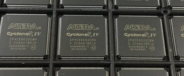
The EP4CE6E22C8N is a type of field-programmable gate array (FPGA) that boasts a wide variety of features and capabilities. Its employment extends to various industries. Aerospace, defense, telecommunications, and automotive are the common examples. However, similar to any electronic device, it may encounter dilemmas that require meticulous investigation. In case you are currently utilizing the EP4CE6E22C8N, then you are on the right page. We are going to discuss the issues and problems related to this EP4CE6E22C8N FPGA. Interestingly we are also providing solutions or reasons for that particular issue. First of all, you must have some basic information regarding EP4CE6E22C8N FPGA. It is related to their specifications.
Know About EP4CE6E22C8N FPGA
Before we dive into the common issues, let’s take a moment to review the EP4CE6E22C8N’s specifications.
This FPGA has 62208 logic elements and is manufactured by Intel.
It has 4140 kilobits of embedded memory. so it can store large data sets
It also has 324 Input and output pins and supports up to 400 MHz of Performance. That’s why it shows super efficiency
The EP4CE6E22C8N is based on the Cyclone IV E family.
There are several issues, but we list a few. That’s why it is easy to understand the main reason and find the solution.
Power Issues Possible Reason and Solution
One of the most common issues with the EP4CE6E22C8N is power-related problems. These issues can vary from situation to situation. For example, insufficient power, power spikes or fluctuations, and inadequate grounding are all power issues. These issues occur when the FPGA is not getting enough power. Sometimes too much power is also problematic. Power supply issues can cause several problems, such as Overheating and Loss of functionality.
Solution
Resolving the power issues is quite easy. Start by checking the voltage levels and ensuring that the power supply can deliver the required voltage. You can also use an oscilloscope to check for power fluctuations and spikes. Last but not least, check your device for proper grounding.
Configuration Issues Reason and Solution
Another common issue is configuration issues. Most hobbyists or mature designers face these
Issues.
These issues arise due to incorrect or incomplete configuration files and incorrect configuration settings. Sometimes neglecting the configuration-related errors becomes problematic.
Solution
Whenever you start configuring, be vigilant to avoid configuring issues. If any issue arises, then try to find out the root cause. You can start by verifying that your configuration files are correct and complete.
Check the JTAG connection to ensure that it is functioning correctly. If the problem persists, consider checking the hardware for any damage. You can also use any Analyzer to debug configuration-related errors. Using debugging tools to find and auto-correct the debugging errors is advisable. You can also take help from a professional or expert for expert opinion.
Pin Mapping Issues
Pin mapping issues can also cause problems when working with the EP4CE6E22C8N. Pin mapping errors.
Occur when the FPGA pins are not correctly mapped to the design files. These errors can cause several problems, such as incorrect functionality, Loss of data, and sometimes System crashes
Solution
To fix pin mapping errors, ensure that you have correctly mapped the pins to the design files. This is the major cause of pain-related issues. Check the datasheet for the FPGA to determine the correct pin mapping. You can also consider using the Quartus software to check the pin mapping.
Clocking Issues
Clocking issues are another common problem that users experience when working with EP4CE6E22C8N. These issues occur when the clock signal is not correctly synchronized. Clocking issues can cause several
Problems. For example System instability and Loss of data are clocking issues. In addition incorrect functionality is also common.
Solution
To fix clocking issues, you need to ensure that the clock signal is correctly synchronized. Check the datasheet for the FPGA to determine the correct clocking specifications. You can also consider using the Quartus software to check the clock signal.
Overheating
Overheating is a very common and most common issue. Most of the users experience it when working
With EP4CE6E22C8N. Sometimes overheating is linked due to power issues. That’s why it is necessary to troubleshoot the power issues. Sometimes overheating occurs when the FPGA is not dissipating heat correctly. That’s why again, it is important to find the root cause. Overheating is the main reason for several other issues, such as Loss of functionality and system crashes.
Resolve power issues and provide proper voltage to FPGA. Make proper arrangements for heat dissipation in FPGA. You can use cooling devices specially designed for EP4CE6E22C8N.
Design And Layout Issues
Design and layout issues are common when working with EP4CE6E22C8N. There are several reasons of
It. For example, using the appropriate degassing software and don’t have enough skill to define the FPGA design layout.
Solution
To surmount the myriad of design and layout quandaries, follow the following tips. Ensure when working with FPGA, especially with EP4CE6E22C8N, is crucial to adhere to a set of superlative customs. For example, it is important to define clear design goals. This will, in turn, ensure the optimization of the design for the specific application and, more importantly, obviate needless design iterations.
Employing a hierarchical design technique is an effective stratagem in deconstructing intricate designs. Furthermore, you can break down complex designs into simple steps. Achieving each design step successfully will improve the design but also its efficiency. In addition, it allows more manageable modules and less routing congestion.
Wrapping Up
Designers must adhere to optimal procedures for FPGA design to resolve such problems. These include meticulous timing analysis, power optimization techniques, signal integrity analysis, and routing, as well as thermal management. Moreover, simulation and analysis tools can be employed to detect and fix design issues prior to hardware implementation. Additionally, designers can seek guidance from FPGA vendors or other specialists to acquire insight into the best practices and solutions for specific design and layout issues.
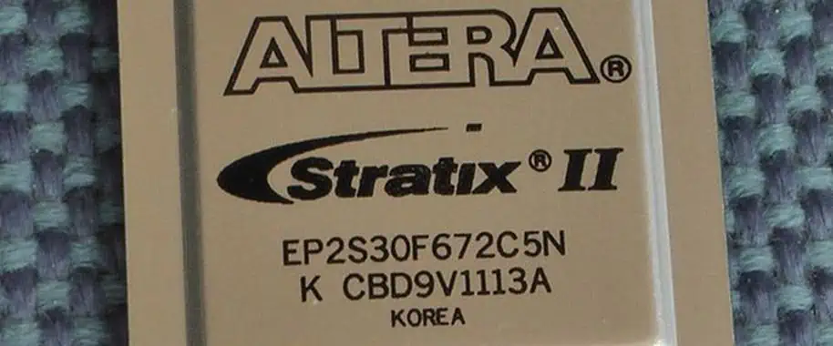
EP2S30F672C5N is a field-programmable gate array. It is produced by Intel. It is a high-performance device. This FPGA offers a myriad of unique features that make it suitable for use in various applications. Almost every modern electronic device has this FPGA. It provides the flexibility to perform complex operations on the hardware level. EP2S30F672C5N is one such FPGA chip that is designed for high-performance applications. Let’s dig deeper to know more about its amazing FPGA. What are its applications?
What Is EP2S30F672C5N?
EP2S30F672C5N is a member of the Stratix II family of FPGAs. Intel is the producer. It is built using modern 90nm process technology. It contains 31,680 logic elements. This FPGA also has 1,620 kilobits of embedded memory. That’s why it is suitable for use in high-performance applications. Similarly, it is ideal to use in applications that require memory resources. It operates at a maximum clock frequency of 600 MHz. As a result, it can handle up to two million logic gates.
EP2S30F672C5N is a versatile device. Due to its versatility, it is part of various applications. Here are some of the common applications of this modern
High-Performance Computing Tasks
EP2S30F672C5N is designed to deliver exceptional computing power, making it an ideal solution for high-performance computing applications. From scientific simulations and data analysis to financial modeling and artificial intelligence, this device can easily handle even the most complex computational tasks.
FPGA utilization, such as the EP2S30F672C5N, in high-performance computing can offer flexibility due to its programmability. These FPGAs have the capacity to execute specific functions, with the ability to modify or update their programming as necessary. As a result, this offers a greater degree of customization and optimization for hardware in specific applications. As a result, its demand is increasing.
Speedy Digital Signal Processing
EP2S30F672C5N also finds its application in digital signal processing. The device’s high-speed processing capabilities and built-in DSP blocks make it an ideal solution for digital signal processing applications. That’s why it is part of many audio and video processing and speech recognition machines.
Embedded Systems And Data Acquisition
EP2S30F672C5N is an ideal solution for embedded systems applications. It is just because of its small size and low power consumption. This FPGA helps implement various functions, such as control systems and data acquisition. In addition, communication interfaces make it a popular choice in different industries, especially in consumer electronics. Portable consumer electronics mostly require low power consumption and embedded systems. That’s why these are portable and easily changeable. As their popularity is increasing, their demand is also growing. As a result, almost every other consumer electronics has this EP2S30F672C5N.
Aerospace And Hi-Tech Navigating Systems
EP2S30F672C5N has high-performance computing and data processing capabilities. Almost every field is getting benefits from it. That’s why it is also an ideal solution for aerospace and defense applications. If you observe, you find numerous systems have EP2S30F672C5N FPGA.
From satellite communication systems to radar imaging, all have FPGA. Similarly, missile guidance and navigation systems have this FPGA. Due to its unique properties, EP2S30F672C5N is part of most complex aerospace and defense applications. Moreover
EP2S30F672C5N’s possess not only numerous benefits, but they also boast effortless maneuverability and installation procedures. It can integrate seamlessly with other systems and pre-existing mechanisms. That’s why its demand is increasing in this industry. In addition, it is an economical remedy for a plethora of aviation applications.
Industrial Automation For More Control
The EP2S30F672C5N is a versatile device that finds its application in various domains, including industrial automation. In the realm of industrial automation, this FPGA is doing wonders. It is employed to enhance the productivity and efficiency of diverse processes. The EP2S30F672C5N is making process control and motion control more seamless and precise. It is part of many robotics for process control. Its built-in peripherals and high-speed processing capabilities make it an ideal choice for automation. It is doing wonders in streamlining industrial operations. That’s why The EP2S30F672C5N is leveraging and regulating the movement of machines, including CNC machines and conveyors of industrial automation systems. Additionally, this device is also suitable for performing image processing tasks, such as object recognition, tracking, and measurement, in machine vision systems. Last but not least, The EP2S30F672C5N has significant potential in process automation. Process automation has revolutionized many industries. It is part of many monitoring and controlling machines for industrial processes. In addition, it is also part of manufacturing, chemical, and assembly processing machines.
It is not a question of better or worse FPGA. It is a matter of compatibility. If EP2S30F672C5N suits your needs and requirements, then it is the best FPGA. Overall it has the best features. In addition, better FPGAs are in the market, but again, it is a question of compatibility and reliability. So you can compare its features with other viable FPGAs.
How can I recognize EP2S30F672C5N in the package?
It is so easy. The packaging for EP2S30F672C5N is a plastic flip-chip ball grid array. This FCBGA contains 672 balls. So it is quite obvious form the packaging. You can look for a small black square chip with a size of approximately thirty-one mm x thirty-one mm on the package. The FPGA will have a pattern of small metal balls on the bottom side. Additionally, the packaging may also have a label. This label conation all the necessary information. It also conation the manufacturer’s logo and part number. That’s why it is easy to recognize. In addition, you can take help from the seller or dealer. So there is no need to worry about recognition.
Wrapping Up The Things
EP2S30F672C5N is a versatile FPGA. It offers high performance, low power consumption, and high integration density. That’s why it is in high demand in many industries. This FPGA is an ideal choice for businesses that require a high level of flexibility in their industrial automation systems. Last but not least it is a great choice for an embedded and compact system.
It’s critical to choose the best PCB layout software for you. Let’s contrast OrCAD with Allegro circuit board Designer to aid in the process. Both this software from Cadence is strong ones for efficient PCB design.
OrCAD provides a variety of add-ons and features, including Capture, Pro PCB Designer, and circuit board Promo Bundle, a whole suite that combines all the aforementioned applications.
Cadence’s premier PCB layout editor is Allegro. It serves as a fully functional, scalable layout solution. The majority of their functions are comparable because they share the same database and libraries. However, Allegro has more functionality that may be required for projects and routes that are more complicated.
Top 10 Differences: OrCAD vs. Allegro PCB Designer
orcad PCB
Both OrCAD and Allegro have specific variances in their capabilities because OrCAD is used largely for schematic design and capture, whereas Allegro is utilized for PCB design.
For primary to medium projects, it is recommended that you begin with OrCAD, and for more sophisticated ones requiring big teams that may require working together remotely or companies that are production-oriented, Allegro should be scaled up.
Since the developer is one, several characteristics of the UI are comparable. Therefore, understanding one software makes using the other software much simpler. OrCAD, however, could be simpler to use for novices.
The top ten differences between Cadence Allegro and OrCAD PCB Designer are:
1. Miniaturization
The miniaturization function, which is exclusive, is the most significant distinction between Allegro and OrCAD.
This process has to do with PCB component embedment. The process of miniaturization involves shrinking the components. Compact hybrid microchips are useful in many low-weight devices, including wearable technology and medicine.
The Allegro Circuit board Miniaturization feature helps with Via’s compact stacking. The program offers combinations of buried and blind vias to transition between circuit layers for tighter packing, consuming less space due to limitations in layer structure manufacturing.
Along with checking the necessary clearances and cavity space for optimal component fitting, it matches the part height to the layer stacking and verifies the design’s validity for HDI boards using DRC.
2. RF Feature or Analouge
An RF layout remedy for the different difficulties designers have when integrating RF components in combined-signal layouts is an Allegro Circuit Design Analogue/RF capability.
To assist designers in producing a mixed-signal layout within a ready-for-production board layout workspace, this feature unifies the capability of both Agilent ADS and Allegro design environments. The Allegro layout Entry-HDL & Allegro Circuit Editor is useful for doing this.
The RF/Analogue is equipable with a number of features. This includes parameterized etch component creation, rapid assignment, RF-style routes, RF etch component editing, and the ability to install through arrays across user-specified entities like RF components, connect lines, or discrete components.
The resulting etch components are classified as parameters-based RF components. The program will automatically renew the updated components if the settings are altered.
3. Systems for Information of Components
In OrCAD, all of the capabilities associated with the component data systems are elective and must be bought individually as extra packages. Allegro Circuit Board Designer comes with these.
These packs come with features including a centralized part data system, infinite assembly variation support, and database support of ODBC-compliant. Furthermore, Crystal Reports supports sophisticated PCB description, the query of the intelligent database, graphical preview, and more.
While OrCAD Designer Professional and Standard editions do not have these functions, Allegro Designer does.
Advanced Placement tools are available in Allegro Circuit Designer for quicker and more accurate circuit constructions. The following are some placement-related capabilities that are accessible in Allegro yet unavailable in OrCAD:
A function that enables a speedier and more intelligent flow plan for the circuits is called FPAM, or flow planning implementation mode. This helps prevent subsequent design modifications or mistakes.
Allegro’s Placement Replication function enables you to store the putting order once you’ve established a placement design so you may use it on further boards.
The DFA or layout for Assembly norm verification in real-time is another useful feature. To assist you in creating an effective and legitimate design, the program dynamically analyzes the legality of the real-time placement against DFA as well as flags any violations.
PCB layout also heavily relies on a different subject called DFM or Layout for manufacturing. Although Allegro offers a few more functions like BoM creation and documentation production, Allegro & OrCAD both offer DFM functionality.
5. Modern Direction-finding
The most crucial component of a successful design for PCBs is routing. Both the OrCAD and Allegro designers from Cadence include a number of tools to assist you in creating well-routed PCBs.
However, Allegro offers a few more capabilities to aid customers in overcoming challenging routing issues. Contour Routing or Flex, interactive late tuning, and bumps are a few of these functions.
Additionally, allegro have shape-based bend fillet support, pointed traces for complex designs, and the ability to re-space/resize different pairs during routing. Additionally, users can split over void recognition and create lines across Anti-pads.
Allegro also includes a HUD, which shows crucial characteristics and real-time information for increased efficiency and simplicity of routing.
AutoRouting: To assist in resolving challenging routing issues, Allegro and OrCAD Designer Pro Version both include specific auto-routing features.
OrCAD basic Edition does not offer these capabilities. The capacity to operate with six signal layers concurrently, with no restriction on layer or pin count, is one of this aspect’s key benefits. 45-degree/memory sequence routing, gridded or shape-based routing, fanouts of SMD, and interactive floorplanning.
Additionally, Allegro users have access to online DRC or layout rule checking and width tracing by the net classes and the net. Additional capabilities, of which some are exclusive to high-end applications, include crosstalk controls and enhanced component interaction like flip, align, rotate, move, and push.
6. Manager for Constraints
A control setting system is called Constraint Manager. Users can establish hierarchical principles and implement them in a network or a whole structure to build a bus, pin pair, or differential pair.
Allegro Sigrity Signal Integrity or SI Base offers a constraint manager. While OrCAD also contains a Constraint Controller system, it differs from Allegro in a few ways.
These consist of region rules, one-line impedance rules, dynamic phase management for differential pairs, relative propagation rules, and minimum and maximum propagation rules. Custom limitations may be imposed for all these features with Allegro Circuit Designer.
Moreover, the Allegro software also has a rule set of Electrical constraints or ECSets. It is possible to verify more complex electrical limitations and rules like formulae, reflection, relational, crosstalk, and timing.
7. Plans for Pricing
There are two versions of OrCAD Circuit Designer: Basic and Pro. Allegro costs considerably more than OrCAD. Comparing Allegro to OrCAD, the price difference is enormous.
After enrolling on the site of Cadence, users may access both apps’ limited-time free trials. For instructors and students, the company also provides longer trial versions that may be accessed after signing up.
An OrCAD Basic Designer Yearly License costs around $1300.00, with extra charges for additional packages. The pricing of a basic version yearly subscription for the most recent version of Allegro Circuit Designer ranges from $2800.00 – $3000.00. One may add more options, but it will cost more.
On the official website of Cadence, a quote may be sought for the precise cost based on your demands.
A yearly maintenance contract is included in both packages, guaranteeing an upgrade for free to the upcoming edition.
8. Simulations and Integrities for Signals
Comparing Allegro to OrCAD Circuit Designer, Signal Integrity or SI capabilities are more sophisticated in Allegro.
Along with the OrCAD simulation capabilities, including noisy transmission lines, simulation, and different-pair exploration. Allegro also offers post-route signal and uni-net extraction analysis.
The SI feature is crucial when working on huge, intricate projects with several layers and greater pins and parts. The SI assists the designer in ensuring that the packing and routing do not, in any manner, degrade the board’s performance.
Additionally, Allegro automatically detects, extracts, and analyzes networks that lead through discrete components and interrelated differential signals.
FPGA Design: While editing, Allegro enables users to exchange pins in accordance with FPGA or Field Functional Gate Array standards. Additionally, it has the ability to use the FPGA Network Planner option to re-optimize pins within the FPGA in accordance with relevant regulations.
Here, OrCAD triumphs against Allegro Circuit Designer. Many people agree that OrCAD is simpler to understand and use than other tools.
Allegro’s extensive features and workspace may frighten new users with no or little expertise in design. On the contrary, OrCAD features a considerably more user-friendly interface and strategically positioned controls.
Along with helpful user manuals and guides, OrCAD Circuit Designer also includes instructional films and visuals. In contrast to Allegro, these substantially assist novice users in getting up and running quickly with project design and development.
For individuals who do make an effort to study Allegro, it may prove useful in the future. Small firms that begin with OrCAD Designer can eventually move up to Allegro because this serves as a scalable platform.
Because every designer who may want to become an expert will eventually have to work on higher-end boards with fast connectivity features, numerous layers, Microwave/RF modules, etc., therefore, it is best to learn how to use the advanced capabilities of Allegro as well.
10. Design Intelligence and Modern Features
We will examine the extra advanced functions that significantly increase working productivity and save design time after going over all the essential aspects of PCB development.
Under Planning Intelligence, Allegro Circuit Designer has several incredible capabilities. Like the TimingVision sophisticated timing closure generator, the ability to create X-nets, F2B reusable modules, and the capacity to specify area constraints by layer.
Allegro has expanded rigid-flex design features, such as variable zone allocation with the automatic drop-down, inter-layer DRC, the ability to generate curved fillets, and curve routing while pushing arc routes.
Besides, Allegro also offers features such as the Microvia database aspect, which is used as interconnect across layers, the capability to delete unwanted vias, and DRC for layered micro vias to assist developers working on applications with HDI frameworks.
Moreover, Allegro Designer has various useful tools for users that need to operate on integrated component designs, including the capacity to indirectly or directly attach integrated components, verify the max cavity size via DRC, and execute cavity height inspections.
Orcad Vs. Allegro? Choose the Best
The correct response to this question depends on several variables that are unique to each designer.
Allegro Circuit Designer will be the appropriate response if the functions and features need to be considered. It offers many of the greatest features on the market and a quick, strong design processor, which renders working on even the most difficult projects simple.
However, if user-friendliness and simplicity are taken into consideration, OrCAD Circuit Designer would win out. In comparison to Allegro, this program is significantly easier to use, and newbies will perceive the process of learning to be considerably less steep.
Allegro, among the top PCB software for design options right now, is a great option for seasoned users who aren’t concerned about the cost.
Additionally, this is based on your needs. Allegro provides cloud-working resources with its Symphonic Team Design capabilities. This enables real-time updation and remote working for enterprises or projects involving big teams. Allegro’s drawback is its exorbitant price.
OrCAD offers many of the more advanced capabilities for more complicated design, with a considerably shorter learning curve. Along with a significantly lesser cost, assuming you doesn’t especially need software for complex designing. Therefore, choosing between Allegro and OrCAD PCB Designer depends on your specific design requirements.
This Allegro and OrCAD PCB Designer contrast article should have been helpful in assisting you in making an informed decision on both of this Circuit Design Software.
Electronics employ circuits as closed paths for the flow of electricity. A primary circuit comprises a conductor, a current source, and the load. Moreover, “circuit” may denote any established path for data, electricity, or signal transmission.
PCBs patterns are arrangements of electronic components and conductive pathways on a circuit board. These patterns consist of copper traces that link multiple features, including resistors, integrated circuits, and capacitors, forming the complete course.
The effectiveness of an electronic device is heavily reliant on the design of its PCB pattern. It is vital to carefully plan and optimize the pattern to facilitate efficient transmission of electrical signals among components and prevent signal interference. Various techniques, including trace routing, ground plane design, and component placement, make an ideal circuit pattern.
To design a PCB pattern, engineers can utilize specialized software like Altium or Eagle. These programs allow them to make a schematic structure of the board. It is then automatically transformed into the corresponding Printed circuit board layout. When a pattern is finalized, it is printed on the copper-clad circuit board. The unwanted copper can be removed through a chemical procedure known as etching.
Electrons leave the electricity source in the electronic circuit and pass through conductors. They traverse a load to execute a task before returning to a head. The circuit’s circular path through which electrons flow is why it is named as such. Ohm’s Law delineates the connection between electrical current and resistance. Within a circuit, electrons move from the negative to the positive side of the energy/power supply.
PCBs are commonplace in advanced electronic appliances, with circuit traces serving like conductors. These circuit boards include all the necessary connectors and components for a circuit to fulfill its intended function.
Integrated circuits enable circuit miniaturization and can be printed on the substrate. The IC includes all essential circuit traces, transistors, capacitors, and other components needed for the intended function. In many devices, the IC mounts onto a printed circuit board or is connected to the power supply.
When the route for electric current is severed, preventing it from flowing in the complete circuit, it is referred to as the open circuit. In such a scenario, electricity cannot flow, & and it does not do any work.
When the electrical route is established directly from the power supply’s output to its input, it is known as a short circuit. Since electricity tends to follow the way of least resistance, the current will flow through the small circuit and bypass the intended load. It can result in malfunctioning of the course and may cause damage to a power supply, overheat the components, and pose a potential fire hazard. To avoid damage caused by short circuits, a fuse and the circuit breaker are added to the circuit. They disconnect the electric route if an excessive current is consumed due to the shortboard.
Circuit board patterns in networking and telecommunications
Telecommunications rely on a circuit to provide a continuous path for transmitting messages from the transmitter to the receiver or back. In the early days of telegraphs and telephones, a complete electrical pathway was necessary to establish communication between the two points.
Within telephony, a voice link/connection is regarded as a circuit, or the number of concurrent courses, or calls, is the metric for measuring telephone system capacity. Circuit-based networks establish physical circuit board connections automatically. So In the case of switched fiber networks, instead of showing an electric circuit, the route that light takes is altered.
Despite the absence of a physical electrical connection in contemporary networks, a “circuit” is still employed. In such situations, the circuit may refer to a data packet’s path as it travels through a network. In the packet-switched network, virtual circuits can be created to establish dedicated routes for specific packages, as with Ethernet and the Internet. The PVC denotes the Logical network path based on another system/network for the undetermined period.
PCB patterns describe the arrangement of conductive routes or electronic elements on PCBs. You can construct PCBs from insulating materials like plastic or fiberglass, with etched conductive pathways that serve to join the electrical components.
This article covers various PCB patterns, each having its distinctive layout and design. We will explore some popular PCB patterns or their uses.
1. Single-Sided Circuit Board
A single-layered circuit board, also called a single-sided PCB pattern, comprises a sole copper conductive substance layer on a single side of a board. These circuit boards are relatively straightforward and cost-effective to produce and are frequently utilized in essential electronic gadgets such as toys, remote controls, or calculators.
2. Double-Sided Circuit Board
The double-layered PCBs feature conductive substances on the sides of a circuit board, which permits the inclusion of a more significant number of components on the circuit board. Due to this ability, it is appropriate for intricate electronic devices like computer peripherals and audio equipment. Although manufacturing double-sided circuit boards is more complicated than single-sided ones, they are still low-cost.
3. Multilayer Circuit Board
A multilayered PCB is a composite of multiple coatings of conductive material or insulation. These circuit boards are utilized in sophisticated electronic gadgets like smartphones, computers, and tablets. Though multilayer circuit boards are crucial for high-operation electronic devices, they are notably more costly to create than double or single-sided boards.
4. Flexible Circuit Board
A flexible PCB is a circuit board fashioned from an insulating material like polyester or plastic. You can use these circuits when versatility is necessary, such as in wearable technology or medical equipment. Although flexible PCBs are more costly than rigid circuit boards, they offer benefits like being lighter or more long-lasting.
5. Rigid-Flex Circuit Board
The rigid-flex board is a blend of the characteristics of rigid or flexible PCBs. These boards are employed in scenarios that require flexibility but also demand specific components be firmly fixed, like in aerospace applications and medical equipment. Although rigid-flex boards are pricier to produce than either flexible or rigid boards, they provide benefits such as lower weight and enhanced reliability.
To summarize, PCB patterns refer to the arrangement of conductive paths or electronic elements on the PCBs. various circuit board patterns exist, each with its distinct layout and design, and are utilized in different electronic gadgets. Whether designing a straightforward calculator or a high-operation smartphone, comprehending the various circuit board patterns is critical to producing effective and dependable electronic devices.
The circuit is a path that allows something to move around in a loop. In the electronic circuit board, the thing that moves is an electric charge by electrons. The electrons come from a positive end of a power source, and they move through the circuit until they reach the opposing end of the original. Different parts of the course can affect how the charge carries. Some elements might make it harder for the charge to move, while others might store or use up the charge. Some parts need extra energy to work, while others provide power.
We may need to build the circuit for various reasons, like lighting a lamp, running a motor, etc. These are called loads, and each load needs a specific current and voltage to begin working. This voltage could be the constant DC and an Alternating Current voltage. But we can’t make a circuit with just a source or the load. We require other components to help the charge flow correctly and to regulate the amount of charge that goes to a load.
Step 1: Designing of Circuit
To create the circuit board, we must know what components we need and their values. In this example, we will learn how to design a regulated Direct current power supply board/circuit.
1. Regulators
In this particular case, we need a constant positive 5V voltage at 20mA. To achieve this, we must have a controller that can provide the 5V output, such as the LM7805 regulator IC. We also need to count the lower input voltage required for a regulator. For our 5V creation, we require a minimum 8V voltage, but we will choose an input voltage of 12V.
2. Transformers
To power the LM7805 regulator and obtain a regulated 5V at 20mA with positive polarity, we need an unregulated voltage of at least 8V. To get this input voltage, we will use a transformer with a secondary 12V RMS. Since the main current is 230 voltages RMS, the ratio of the transformer will be 19. Therefore, we need a 12 voltage of current, 20mA of transformer with a 230V primary voltage.
3. Filter capacitor – Values
The capacitance value of a filter capacitor relies on various factors, including the load’s current consumption, the regulator’s quiescent current (the ideal current), the permissible ripple in Direct current output, & the period.
To get the highest voltage of 17V (12 x sqrt2) across the converter primary and a total drop of 1.4V crosswise the diodes, the highest voltage over a capacitor is approximately 15V.
So you know the required components and how to connect to the circuit. It’s time to draw the circuit by software & simulate it.
The following steps outline how to create a circuit utilizing Multisim and perform a simulation.
1. To access Multisim 11.0 on Windows, navigate Start to Programs to National Instruments and then Circuit Suite Version 11.0 to Multisim version 11.0.
2. After opening Multisim software, you will see a window with a menu bar. You will also see a blank space that resembles a breadboard. You can use it to create the circuit.
3. From a menu bar, choose “Place” and then “Components” to access the component library.
4. A window titled “Select the Components” will appear.
5. In the “Database” section, choose “Master Database.” It is present in a dropdown menu.
6. To add a component to your circuit, select the appropriate group from the “Group” section. If you need a voltage & current source and a ground, select the respective group. If you need essential components like resistors or capacitors, select the corresponding group.
For an input Alternating Current supply source, select “Source” and then the “Power Sources” and “Alternating current Power.” Once you’ve placed the component by clicking “OK,” you can set the RMS current to 230 voltage and 50Hz frequency.
7. Next, choose “Basic” from the elements window, then select “Transformer,” and finally select “TS_Ideal” to add a perfect transformer to your circuit. In an perfect transformer, the reactance of coils is similar. To obtain the desired output, we need to adjust the inductance of the second coil.
8. Your electronic design is now ready for testing using computer simulation.
9. Next,click “Simulate” and select “Run.”
10. You should now see the Light Emitting Diode at an output blinking, as specified by the green arrows.
11. To verify if you are obtaining the correct voltage value across each feature, place a Voltmeter.
Conclusion
Conclusively, PCB patterns are crucial in the design or manufacturing procedure of electronic devices. The arrangement of electronic components and conductive pathways on the board plays a significant role in determining the efficiency or dependability of a machine. Several types of PCB patterns exist, with distinct layout designs, each suitable for specific applications.
Single-layer PCBs are simple and affordable, whereas multi-layer boards are intricate and costly but imperative for high-operation electronic devices. Flexible circuit boards provide flexibility, whereas rigid-flex boards integrate the characteristics of both rigid and loose boards. Understanding the different types of circuit board patterns is crucial in creating electronic devices that are efficient, reliable, and cost-effective.
If you are producing PCBs for different types of devices and equipment, it is essential to prioritize the board’s heat dissipation capabilities. Effective heat dissipation in PCBs can prevent performance problems and catastrophic failures from excessive temperatures. It is vital to choose a PCB equipped with appropriate heat dissipation components to avoid overheating and to ensure reliable performance.
Discover additional information regarding the issue of heat and gain insights on techniques for dissipating heat in PCBs.
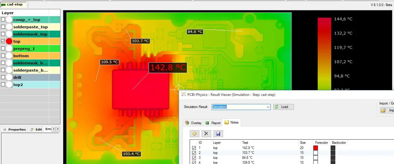
Why Is Heat Dissipation A Problem In PCBs?
The flow of electric current through electronic components results in an increase in thermal load. Various factors, such as the circuit layout, power input, and device properties, influence the extent of heat an electronic component generates. Improper installation of parts, external factors, insufficient ventilation, and incorrect assembly are frequent causes of overheating in PCBs.
While PCBs can tolerate a certain amount of heat, elevated temperatures can result in significant problems. PCBs can experience several adverse effects due to excessive heat, including circuit line disruption, component oxidation, compromised structural integrity, and incompatible material dilation rates. These consequences can lead to a decline in the PCBs’ overall performance. If the PCB is exposed to excessive heat for a prolonged period, it can malfunction and even fail, causing permanent loss to the Printed circuit board.
Techniques Of Heat Dissipation In The PCB Industry
heat dissipation in electronic devices
Considering the adverse effects of excessive heat, it is advisable to ensure that your PCB possesses heat dissipation capabilities. To dissipate heat from the Printed circuit board, several techniques can be employed, such as incorporating heat sinks or cooling fans, which are effective means of heat dissipation.
Discover the fundamental techniques for dissipating heat in Printed circuit boards by exploring the following methods:
1. Cooling Fans & Heat Sinks
Heat sinks are metallic components with high thermal conductivity and a significant surface area commonly utilized by PCB designers to dissipate heat. They are typically affixed to heat-generating features such as switching devices, enabling the component to transfer heat to the heat sink and dissipate it over its large surface area.
In addition to incorporating thermal dissipators in your PCBs and other device components, you can install cooling fans. These fans introduce excellent airflow into the device, facilitating rapid heat removal and preventing heat buildup. Typically, you can utilize cooling fans in high-current power supplies, which aid in more efficient and expeditious heat dissipation.
2. Use Thick Copper Traces
When designing a Printed circuit board for high-current applications, it is often advisable to incorporate thick or thick copper tracks. Wide copper traces provide an increased surface area for heat dissipation and distribution, allowing heat to dissipate more effectively.
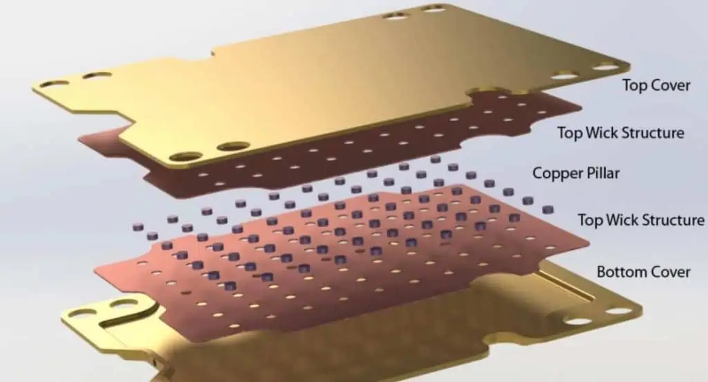
3. Invest in Heat Pipes
In cases where the PCB is present in a compact application with limited space, heat pipes are an effective solution for heat dissipation. So these pipes use fluids like small quantities of acetone, water, ammonia, or nitrogen, to absorb heat. Once the sap gets in the heat and the pipe releases vapor that flows down. The condenser then condenses those vapors into liquid form. It allows the pipe to cycle continuously.
Companies that mostly prefer heat pipes seek a cost-effective and dependable method of passive heat transfer owing to their remarkable heat transfer capability. By incorporating these pipes, devices can attain good thermal conductivity while requiring minimal maintenance. Heat pipes are also incredibly silent, as they do not have any moving parts and are entirely free of vibrations.
4. Right Board Materials
Opting for board materials well-suited to dissipating heat is another technique that can help improve heat dissipation. Certain PCB materials lack the necessary properties to handle high temperatures effectively. Thus, it is crucial to select substances that possess heat-dissipating properties, significantly if your equipment exposes to high heat/temperatures. Choosing the polyimide base is an intelligent Option.
5. For thermal management
Flex PCBs are a suitable choice for heat dissipation because of their thin and flexible substances, which enable a larger surface-area-to-volume ratio. Another excellent option for heat dissipation is aluminum PCBs, which are a kind of metal-core circuit board that features a dielectric layer. So this layer assists in absorbing heat and transferring it to the aluminum layer, where the heat disperses. Aluminum-printed circuit boards are beneficial for high-energy appliances. For high-energy tasks, copper-printed circuit boards offer the best heat dissipation & thermal conductivity.
Ceramic PCBs are an excellent option for high-temperature and high-frequency offerings as they offer exceptional heat resistance and connectivity. These PCBs are usually constructed with either alumina or aluminum nitride and boast high heat conductivity, low coefficient of Heat expansion, and excellent versatility or chemical corrosion resistance. So this makes them ideal for use in a wide range of environments.
6. Use Thermal Via Arrays
To enhance heat dissipation and reduce thermal resistance, thermal via arrays are a great option. They work by increasing the area and mass of copper, resulting in decreased thermal resistance. Additionally, they allow for better conduction and are particularly useful for critical components that generate heat. As a result, you can place thermal via arrays close to heat sources to improve performance.
For businesses seeking to eliminate heat dissipators from their Printed circuit board, thermal via series are a popular option. Thermal via arrays can be combined with a pad in specific applications to conduct heat away from a device. So it improves the Printed circuit board Thermal dispersion and eliminates the requirement for heat sinks.
7. Implement Copper Coin Technology
Tiny particles of copper, known as copper coins, are typically embedded in PCBs beneath components that produce significant amounts of heat. This placement takes benefit of copper’s excellent heat conductivity. It allows the coins to draw heat from the elements and transfer it directly to the heat sink. Copper coin effectively dissipates heat, especially when only a few components generate the most heat.
Several shapes of localized solutions, such as T-Coins, C-Coins, and I-Coins, are available for use depending on the area shape. Once the routing process is complete, one can integrate the coin into a slot in the PCB, laminated & metalized to ensure a secure connection.
To ensure effective heat dissipation in a PCB layout, companies often follow best practices during the design phase. For example, they may place temperature-sensitive elements in more excellent areas, such as the bottom of the device, and avoid installing them on higher levels of heating equipment. Designers may also stagger multiple components resting on a level surface to improve ventilation. To achieve more accurate temperature readings of a PCB, a company may opt to place a thermometer in the Hottest zone.
A well-designed PCB layout prioritizes the installation of heat sources at a safe distance from one another to prevent excessive heat buildup. So, If the cooling fan is present, designers may consider placing high-heat generating elements downstream but installing low-heat Power-generating components upstream to optimize cooling. Professional PCB designers also study the device’s air circulation and strategically place high-heat creation devices based on airflow.
9. Integrated cooling methods
Integrated cooling techniques achieve more excellent thermal conductivity than traditional heatsink and fan setups. The principle involves directing a refrigerant through dedicated vias to the underside of processors, BGAs, or other heat-generating components.
The designer should determine the appropriate number of vias based on the criteria of a mounted element. Initially, the single via may be sufficient, but additional vias may be added depending on the fluid’s velocity and the component’s surface area.
In addition to the previously mentioned Embedded cooling method, there are other approaches, such as the internal cooling method. With this method, a heat exchanger is integrated directly into the board, eliminating the need for an Outside heat sink and cold plate, resulting in reduced weight and Printed circuit board assembly steps. However, these coolers necessitate a high density of thermal vias around the Cooling pathways.
· Cooling fans
This article discusses various cooling methods, including heatsinks, thermal vias, and heat pipes. While these methods rely on conduction to transfer heat, in multiple situations, this alone is insufficient. A cooling fan employs Thermal convective transfer, providing designers with a highly efficient means of dissipating heat from components.
The effectiveness of a cooling fan is determined by its capacity to move a specific magnitude of air from an appliance and its compatibility with the device’s layout. When selecting a fan, designers must take into account factors such as size, cost, and noise. However, the fan’s primary function is to move air, making capacity the most critical factor to consider when choosing the cooling fan.
· Soldering concentration
To minimize heat buildup on component leads, device joints should have even and uniform soldering thickness. Care must be taken when soldering near vias, as there is a risk of overfilling the hole, resulting in bumps on the lower side of the circuit board and a reduced contact area with the heat sink.
To prevent solder overflow, Printed circuit board designers have two options. The first is to reduce the via diameter to less than 0.3mm. With smaller vias, the layer tension of liquid solder in the via can better counteract gravitational force acting on a solder.
Testing is the second way to do it. It means putting a unique cover over the small hole so that when the solder is added, it doesn’t go into the hole.
It’s time to consider upgrading to more advanced methodologies in Printed circuit board cooling, such as thermoelectric cooling/Peltier pump methods. With these techniques, you can cool components to sub-ambient heat.
TECs are a preferred cooling solution in applications requiring precise temperature control, such as CCD cameras, microprocessors, laser diodes, and night-vision units. TECs provide Exact temperature management or faster response times compared to traditional cooling methods. Designers can combine TECs with air and Liquid cooling methods to increase the cooling capacity. It also extends the limits of air cooling for power processors.
10. PCB thermal vias design
The copper barrels conduct heat and run through the board from top to bottom. They are efficient Heat conductors that conduct heat away from essential electronic components. It makes them helpful in facilitating heat reduction from SMDs.
If there isn’t enough space on the upper side of the Printed circuit board for the cooling system, such as in the case of an integrated sensor or indicator. Or a densely packed board, one way to dissipate heat is by using thermal vias to transfer heat to the cooling unit, such as a heat sink and heat pipes.
In PCB thermal design, the width and thickness of copper pads or traces are crucial factors. The thickness of copper traces should be enough to offer a low-impedance way for the current flowing through them. The resistance of copper vias can cause significant power loss & heat generation, especially when they carry high current density. Therefore, we recommend sufficient trace thickness and width to minimize heat generation.
12. Minimizing Heat’s Impact on PCBs
Having learned the tactics, it is now essential to have a strategy to implement them. A critical process is to Divide the heat-generating elements from the heat-sensitive on the PCB. It allows for Directed Heat reduction efforts in a specific area and Prevents heat from affecting the Temperature-sensitive components.
When mounting the Printed circuit board vertically, we recommend placing heat-producing components on the top side. Additionally, it is beneficial to identify these components towards the side of the Printed circuit board. It reduces heat dissipation in an environment.
There are several regulatory issues for defense and aerospace electronics firms to consider. The majority of legislative regulations and commercial requirements for domestic PCBs and electronics are in place to guarantee quality, dependability, worker safety, and environmental safety.
There are further severe laws regarding who is permitted access to technical information on defense and aerospace electronics, even if these rules are meant to safeguard the end user and the general public.
ITAR and the EAR are the most important of these for PCB design and defense contractor companies. ITAR is the most crucial between the two for producers and designers in the aerospace and military industries: Defense equipment is governed by ITAR, and everything else is governed by EAR. Who may manufacture, transfer, read, or retransmit defense publications for their own use or on behalf of other organizations is governed by ITAR.
When developing new devices for the systems they manufacture, defense and aerospace electronics firms should think about how to work with a PCB layout company and permit ITAR circuit board manufacturing.
In 2008, for the sake of national safety, the American DoD reinforced the contractual limitations on federal contractors. Despite the fact that no new rules were introduced, this decision increased the risk that a corporation partnering alongside the DoD would violate its contract, leading to penalties or an inability to keep working together with the federal government on defense projects. Companies that provide goods and services to the DoD as well as other defense agencies, have subsequently increased the requirements that suppliers and other parties abide by international trade laws like ITAR.
An organization can demonstrate ITAR compliance by joining the DoD Trade Controls of the US State Department. A PCB or electronics designer, manufacturer, or developer who registers promises to abide by the ITAR’s regulations and rules with regard to products on the US Munitions List or USML. The USML has items that you may imagine need restriction, like armored vehicles, tanks, and various other platforms utilized for defense. It also covers less evident technologies like software, data, and commercial satellites. Therefore, it is important to take precautions to make sure that, if required, you are functioning in conformity with ITAR.
When Do You Need the ITAR PCB Compliance?
If you aren’t a military contractor or don’t frequently supply DoD suppliers, you might not normally think about whether it’s necessary to stay ITAR compliant. As an alternative, you may base your decision on the customer.
However, it is preferable that you should know the time when or how ITAR compliance begins to impact your development and design. Also, owing to the fines and the possible consequences for being unable to fulfill these regulatory standards. Making this decision is aidable by requesting the following queries.
If none of the inquiries above can be answered with a solid “no,” you should look into it further to find out for sure whether ITAR compliance is necessary for your company’s growth. If thus, you can read more here about how to register.
One of the DoD’s and other federal agencies most important tasks is to monitor and limit access to military systems from individuals who do not specifically require it. You play a key role in that limitation apparatus. If you develop and manufacture the electronics and PCBs employed in these systems. For the development, you ought to work with an ITAR-registered CM or contract manufacturer, such as Tempo Automation.
ITAR PCB Compliance Vs. ITAR Registered
According to ITAR, everyone (or any entity) engaged in the production of defense goods or the provision of defense services must register with the US State Department and maintain their registration up to date. The Department has registered Epec Engineered Solutions and Technologies.
Although they do not have the necessary measures for registration with the US Department, many businesses assert that they are indeed ITAR compliant. If you are in charge of managing ITAR materials, it is solely your duty to ensure that all the suppliers are registering properly and following the ITAR regulations. ITAR is interpreted and implemented by the Department of State. Its mission is to protect the national security of the US and advance its foreign policy goals.
ITAR compliance necessitates considerable dedication from the administration and a big investment in infrastructure for a worldwide manufacturer of products. The management of Epec has committed to keeping all of ITAR’s data in a way that goes much beyond what is required. This happens under the ITAR by making investments in secure and separated IT resources.
Understanding ITAR PCB And Supply Chain
Since Epec became a pioneer in the field of managing supply chains, we have developed methods and procedures. These guarantee ITAR compliance both now and in the future. It is our duty as an organization that works with ITAR products to ensure that all the subcontractors, directors, workers, and salespeople are aware that subordination is not a choice. We can methodically verify each of the affected parties to ensure compliance thanks to the auditing methodology. This is just another method that we benefit our clients.
Importance Of ITAR PCB In the Industry
The circuit board or PCB is a term that refers to describe a thin board of fiberglass having electrical channels. Epoxy and laminate substances can also be useful in creating the board. The pathways or traces connect integrated circuits, resistors, and transistors. PCB is useful in many different technologies and is crucial for innovation.
Therefore, it is crucial for businesses in the Circuit sector to maintain ITAR compliance. Moreover, its employment in thermal control systems, laser equipment, and spacecraft, PCB is prohibited due to its military purpose. The compliance of ITAR is essential for the following reasons.
1. Legality
It guarantees that the PCB business abides by the law. If you are producing PCBs without compliance, then you are breaking the law and risk facing harsh consequences. Lower revenue may arise from penalties since you will need to shut down your company to complete the required documentation. In addition, failure to comply might result in severe fines.
2. Better Security Information
You can protect intellectual property by becoming compliant. Other businesses cannot steal the Circuit board you are manufacturing as you remain transparent about its capabilities and can demonstrate that it belongs to you.
3. Peace Of Mind
ITAR compliance guarantees that you may unwind and manage your business. If you don’t comply, you’ll worry about government oversight all the time. As long as you are acting legally, you may unwind.
If a PCB design is going to use in a military product that is listed on the USML, ITAR compliance assures all the technical information needed to create the PCB is limited. No one cannot share or export that information with anyone from other nations. The information includes all the technical artwork, drawings, netlist details, CNC data, ODB++ data, and production specifications. Wholesalers and distributors, as well as manufacturers, cannot sell PCBs without certification.
Companies engaged in PCB manufacturing and assembly must adhere to ITAR regulations. List yourself with the DDTC to be in conformity with ITAR. It lets everyone know that you checked out the ITAR. At the same time, being ready to follow the rules governing the production and distribution of PCBs. Obtaining ITAR Circuit board certification will guarantee that you may export or sell your product with ease. If the government checks your paperwork, you won’t need to be concerned about paying hefty fines.
How To Maintain the ITAR PCB Compliance?
Manage all information given by the client in a way that prevents access from different sources. These are unidentifiable or unauthorizedly origins
Likewise, the electronic product itself is not accessible to unauthorized parties for evaluation or purchase.
Furthermore, the customer is responsible for providing the CM with the infrastructure and/or guidelines essential for safely conveying inquiries or important technical data.