Use Vias On Pads for Designing and Manufacturing PCBs

vias on pads

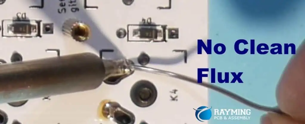
Via stands for Vertical Interconnection access. Vias help in transferring signals from one layer to another layer of a PCB. Let’s suppose the tracks exist on the x-axis and the y-axis of a PCB while vias are present on the z-axis. Generally, they consist of tiny vertical pipes with a coating of conductive layer and put in holes. These holes also use different kinds of filling, which ensure high electrical and mechanical strength.

In a traditional method, if a pin is used to connect vias, it creates tracks that help in routing the signal far away from the pads. Moreover, this method does not suit well for Surface-mounted dense PCBs, BGAs, ICs, and QFN.

This article helps in understanding the Via-in-pad in detail. It describes the vias types depending on their depth. Moreover, this article will surely help you in understanding the development and usage of via-in-pad in various devices and applications.

Introduction

Gordon Moore, the CEO of Intel, in 1956, indicated that the use of transistors in one silicon chip would double every couple of years. However, it was only the beginning. Over the passing years, the component size keeps decreasing.

However, in the late 1980s, the innovation of I’d and the constantly decreasing size of electrical components gave rise to the uselessness of manually designed PCBs. This led to the manufacturing of PCBs with multilayer, flexible variants and high power to boost efficiency.

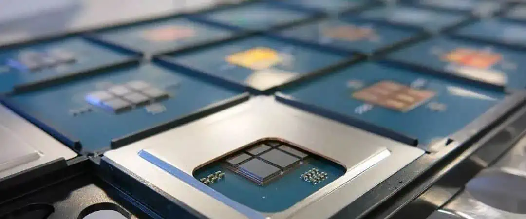
Printed Circuit Board offers a platform and mechanical support to place components over them and create a connection between them. Copper tracks help in creating connections between components in a single-sided PCB while it needs via for transferring signals from one surface layer to other surface layers.

Different Types of Vias On Pads

Via in PCB

Vias come in variant forms depending on their usage and the type of connections they create. Let’s dive into the details of some most commonly utilized vias.

1. Through-hole Via

Through-hole via helps in shorting almost all PCB layers at a certain point. It creates a hole through drilling and then uses conductive copper to coat it. This helps in connecting all PCB layers from the outer layer to the other outer layer, all from top to bottom. 

Because of its simple construction and structure, through-hole vias come in the most common category in the manufacturing of a PCB. Among all types of vias, through-hole vias are the simplest and cheapest to create.

However, a revolution in the advancement of accurate machines developed special types of vias that allowed designers to leave certain layers of a PCB. These specialized vias comprise buried, blind, via-in-pad, and microvia.

2. Blind Via

Blind Vias help in creating connections between the external layer and more than one internal layer. These types of vias can only be visible from one side while invisible from PCBs’ other side because blind via cannot go through the whole PCB. This gives them their name. 

Blind via seems more expensive and complicated to make than through-hole via.

3. Buried Via

Buried Vias help in connecting more than two internal PCB layers. These types of vias do not make connections with the external layer. Thus, one cannot see it from the outer side. Buried vias are only used over the surface of a PCB with more than four layers. This also makes it more difficult to create them than blind vias.

4. Microvia

Microtia refers to traditional vias but in small sizes with certain changes in the structure. Microvias give a similar look to a frustum instead of creating a cylindrical shape. The radius of a micro via keeps decreasing with its transitioning from one PCB layer to the other.

Designers create micro vias to specifically connect two or more layers. However, for creating connections of multilayer PCB, manufacturers place micro vias over the top of one another and stack them. Buried micro vias typically use filling like epoxy conductive substances, which enhance their durability from mechanical pressure and stress.

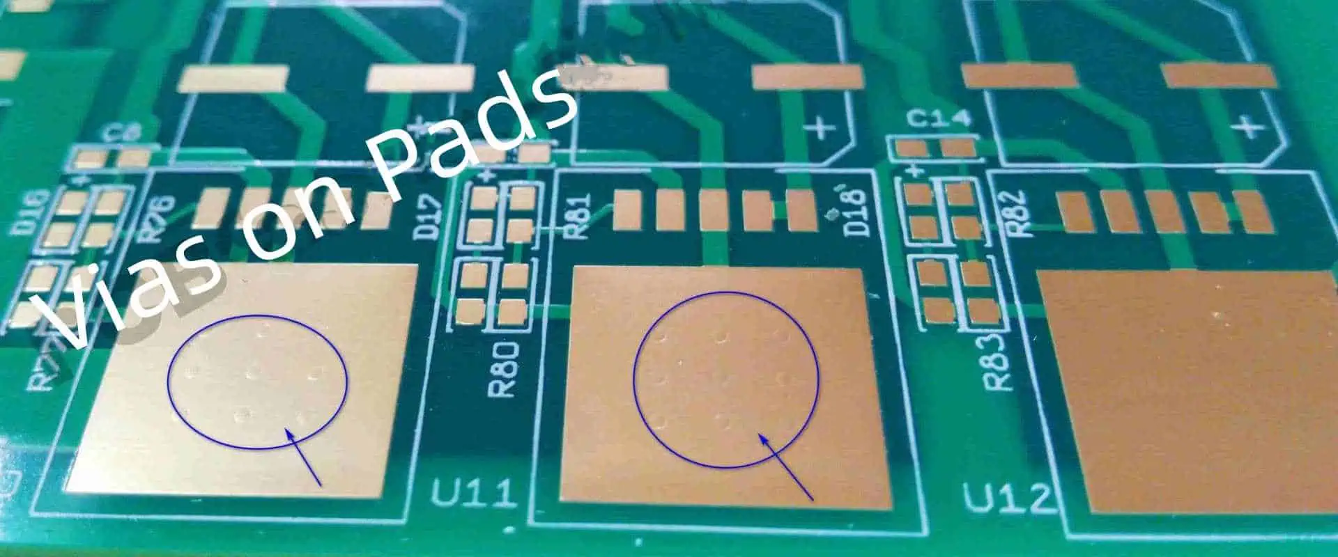
What Is A Via In Pad?

Via-in-pad, as the name suggests, is put inside the pad of electronic components on the PCB surface. They create connections between external layers to all other PCB layers.

However, to understand the Via-in-pad necessity in a PCB, let’s dive into applications with high-frequency and HDI PCBs that use ICs along with a package of BGA.

Applications of Vias On Pads

PCB designers mainly use vi-in-pads in the manufacturing of PCBs when saving space concerns them the most. Via-in-pad is also widely used with tiny BGA package components as they do not allow other vias to fit in it. 

Moreover, BGA packages help in fixing and placing the tiny and compact surface-mount components with various amounts of pins. Components pins in the packages of BGA arrange in a systematic matrix order in which each pin has a tiny solder ball. Contrary to other widely used packages like Dual-in-line, the BGA package allows higher packing ruggedness and efficiency.

The solder ball size and the distance among the closeby BGA pins must be as tiny as a millimeter fraction. This makes the routing of surfaces complicated. Moreover, tracks with smaller trace widths are put out from each pin in an appropriate place for creating vias. Although, this does not seem to be an ideal approach.ย 

In electrical components in which the distance among the pins is smaller than the secure track clearance, then it may lead the PCB design system to give warnings. 

Regardless of routing all pins far away and creating a via away from an electrical component, you can directly put the via right under the BGA pad. This helps in carrying the signals through the pins of components to a specific layer of PCB.

 Advantages Of Vias On Pads Routing

Via-in-pad offers various benefits, which include.

ยท Space Saving

Saving space falls under the primary reason for utilizing via-in-pad in the PCBs. Regardless of sending signals away from a pad in traditional vias, via-in-pad makes a direct connection with the components under the pad. This leads to saving a lot of space. Moreover, it also eliminates the need to create dog-bone trails, which helps in routing optimization and significantly minimizes the whole footprint of a PCB.

ยท Easier Routing

Putting the via right beneath the pads directly not only save space on the PCB but also enables the process of routing simple. Particularly for tiny components with tiny footprints like the BGA package.

ยท Improved Heat Dissipation

Via-in-pad can effectively enhance the dissipation of heat for the power source, which mounts over the surface of a PCB. Nonetheless, putting a via closer to the heat or power source significantly enhances the thermal conduction between distinct PCB layers and components. Thus, it allows heat to dissipate faster.

ยท Reduce Parasitic Inductance

Via-in-pad helps in minimizing the associated inductance by eliminating extra connection parts. Additionally, via-in-pad also enables designers to put bypass capacitors nearby to the electrical components, which helps in reducing the inductance. Therefore, for high-speed interfaces and designs, it mainly helps in the enhancement of signal integrity.

Drawbacks of Vias On Pads Technology

FULL PCB MANUFACTURING Quote

Via-in-pad does have various downsides which affect the functionality of a PCB. Therefore, one must know them to create a functional and error-free PCB design. However, a PCB designer must go through these factors before considering any design for the via-in-pad. 

ยท Higher Manufacturing Cost

The creation of a via-in-pad mostly needs more than a hole drilling and filling it with a layer of conductive material. Via-in-pad needs a type of filling, especially conductive filling or conductive epoxy, to enhance its mechanical strength. However, this may add up in the cost because of the material and some additional steps of the assembly process. The price of via-in-pad manufacturing does not go down with an addition in the manufactured units, which literally increases the connected cost. 

ยท Surface Bumps

When the vias do not place and fill appropriately, it creates surface bumps. However, this surface regulation leads to complications in the components soldering process particularly in ting components with a clear connection. Therefore, while making via-in-pad, PCB manufacturers must make sure that surface bumps must be eliminated. 

ยท Increased Design Complexity

Via-in-pad is quite hard to install and design.

Conventional Vias Vs. Via-in-pad

Although the process of installation of via-in-pad is quite similar to the installation process of the traditional via. However, designers must consider a few factors while designing the PCB and its fabrication process. These factors include:

ยท Verifying PCB Manufacturerโ€™s Design Capabilities

Manufacturers of PCBs set up brief descriptions of their manufacturing process capabilities. However, before choosing a specific design of a PCB, a designer must go through the website of manufacturers to understand distinct parameters and factors. This includes the minimum size of an annular ring to prevent rule check of design or DRC and manufacturability design or DFM issues at the after stages.

ยท Extracting All The Required Files From The PCB Design Tool

Reviewing and evaluating the PCB design after exporting it from the EDA or Design Automation tool helps in solving issues and confusion. Additionally, the file which contains drill maps gives an extra file that contains a via-in-pad map. This ensures that conventional vias will not get filled and capped.

ยท Via Capping

Via tenting or capping is a type of coating process using a solder mask. This helps in resisting the solder paste or solder. Via tenting or capping does not consider an ideal choice for via-in-pad because solder masks cannot apply over pads. Therefore, while manufacturing PCBs, manufacturers need to create capped vias beneath the pad. This aids in preventing the solder mask from sliding inside the holes of the vias. For instance, in some cases, when vias are put beneath the thermal pad, this dissipates the heat better only if the via is uncovered or hollow.ย 

ยท Creating Precision Vias On Pads In Your Design

You may force the design systems of a PCB to insert vias inside the pad. However, this may lead to various checking errors of design rules if the system does not set up to a specific setting according to the technology. You have to ensure that the design software must support this sort of via-in-pad technology, then make a via according to it. After that, set all the necessary rules and configuration of the via-in-pad inside the design software. This helps the systems to accept vias as you inset them. 

To design an efficient design of modern PCBs, one may need a design system of a PCB. Make sure the system offers the necessary features to create various structures and shapes of vias. Also, it must have editing capabilities of rules to create your via-in-pad design. 

However, PCB designer Allegro serves as an ideal choice for this sort of work. It has advanced features via pad stack. Additionally, it owns a constraint editor and fully functions features of design rules. This also allows you to use any type of technology in creating the design of your PCB.

Conclusion

Vias are mainly used for transferring signals electrically between the various layers of a PCB. Via can be put directly under the pads instead of putting a conventional via, which keeps the signal far away from an electrical pin. Via-in-pad helps in saving space, enhances thermal conduction, minimizes parasitic inductance, and simplifies routing.

These types of via cost much more than traditional ones. Therefore, a PCB designer needs to check the manufacturer of PCBโ€™s design capabilities and make sure that they have all the necessary resources, advanced methods, and design tools. So that they offer high-quality products in the end.

A Complete Guide to PCB Encapsulation

PCB Encapsulation

The process of PCB encapsulation has to do with the encapsulation or the filling of electronic assemblies using a compound to offer some protection from vibration and shock, contaminants like chemicals, moisture, and dust, and corrosion. The electronic process of plotting also ensures the protection of the components from any security threats like reverse engineering or tampering.

In contrast to conformal coating, PCB encapsulation is more robust and thicker, which helps in protecting the electronic assemblies from different tin whiskers and harsh environments.

What Does PCB Encapsulation Mean?

Another reliable method for offering protection to the PCBs from any external damage is referred to as PCB encapsulation. You can also call it PCB potting. From the name, encapsulation strives to surround your PCB rather than just adding coat to it. The casing or pot will be built over the printed circuit board and then the fluid will be poured in the casing, thereby sealing the PCB up.

Because they are two major component systems, the process of PCB plotting deals with the mixing of resin and the hardener. Doing this will create a form of chemical reaction, which creates the cross-linked polymer. In order to boost the performance, resin feature mineral fillers, which have greater viscosity. In addition, majority of resins are made to be VOC-free and cure only at room temperature. This is why, PCB coating sprays are not necessary.

Though it is possible to apply a casing of 0.5 mm, usually, they are much thicker than this. With an increase in thickness also comes a weight increase. This leads to higher expenses for each coating. Also, the components will get better protection as a result of the increase in thickness.

Pros

  • Useful for high-volume applications
  • Its dark color provides design security
  • Provides greater protection against chock damage and water

Cons

  • A significant increase in weight
  • More process steps
  • Costlier than the conformal coating

PCB Encapsulation vs Conformal Coating

expoxy potting & Encapsulation

Choosing between conformal coating and circuit board encapsulation isnโ€™t about which method is best, rather it has to do with which of them suits your needs. Concerning this, youโ€™ll consider:

  • The layout and the design of the PCB
  • Its individual components
  • The Use environmentโ€™s expected conditions

If youโ€™ll be exposing your device to very extreme conditions, choosing PCBA encapsulation will be a smart choice. This is because it provides additional protection benefits. These environments include power plants, mines, and manufacturing factories.

Moreover, if flexibility is the major goal, i.e. when dealing with consumer electronics, the better choice will be PCB coating. Electronic encapsulation has to do with offering protection to the electronic assembly using a compound as a form of defense from vibration and corrosion shock.

How to Perform PCB Encapsulation

PCB encapsulation or pcb plotting deals with sealing of the PCB in a thick resin layer that offers great protection from harmful chemicals and physical shock. This process enhances the PCBโ€™s electrical performance.

To perform the PCB encapsulation,. You have to place your PCB assembly inside an open pot and then add some liquid compound in it till the entire PCBA becomes completely covered. This liquid has some hardener in it that helps to speed up the curing, and whenever this liquid solidifies, it plays a great protective role.

Normally, this resin utilized here is dark in color. This makes it very difficult for anyone to see that board under it. The materials commonly used for the plotting compounds include silicone, polyurethane, and pcb encapsulation epoxy.

Different materials come with their own benefits and pitfalls, which should be put into consideration. The applications determine your selection of the best material. For instance, pcb encapsulation epoxy and silicone work best for circumstances surrounding high temperatures. Moreover, urethane will offer a much better performance to chemicals. Therefo4e3, the most important point when choosing the materials is that you need to have a very good thought about the type of protection you desire.

When Should PCB Encapsulation be Used?

 As already mentioned, PCB encapsulation provides great protection performance. Therefore if you want your application or device to be able to stand against abrasion, strong physical shocks, high temperature, chemicals, abrasion, as well as moisture, PCB encapsulation should be the next move. This is because it also includes the vibration damping option.

Also, PCB encapsulation can help in protecting engineering privacy. This is possible due to its colored resin. This makes it difficult for the other people around to see the underneath board region and then make some profit from it.

However, this is a two-edged sword because this invisibility can bring in some obstacles when there is need for a rework or repair. Also, potting is important for all high volume work because it can be handled quickly on any assembly line. Finally, PCB potting provides a great aegis against all electrical arcs. Therefore, if you have high-voltage electrical devices, we advice that you make use of circuit board encapsulation rather than conformal coating.

What are the Benefits of PCB Encapsulation?

FULL PCB MANUFACTURING Quote
  • Encapsulation offers full protection against water damage and shock
  • It provides a well-secure seal that prevents contaminants from entering
  • It protects against chemicals and corrosion
  • A very reliable way of reducing RFI/EMI interference in different devices
  • Electronic components that are encapsulated provides a strong foundation for any wire bonding through the reduction of stress on the solder joints, which might have cause failure or breakage. This elimination of the exposed copper edges offers a reduced surface area for the oxidation. It also offers better adhesion between the solder pads and wires as well as better thermal performance.
  • Encapsulation helps to protect against tin whiskers which are harmful, by creating a form of environmental barrier.
  • It also prevents the components from getting destroyed or damaged because of external forces like mechanical vibration
  • It ensures the best functionality of the device over time. Also, it improves the insulation found between the electrical devices to help in reducing the loss of current
  • The reverse-engineer also finds encapsulated PCBs more difficult compared to those with conformal coating that are applied to some regions
  • Also, it protects the components from experiencing thermal expansion problems. Furthermore, it retains iconic purity as well as properties relating to moisture resistance
  • Generally, PCB encapsulation is faster and less expensive than the other methods of protection. This is because it needs few application steps and doesnโ€™t need reassembling.
  • VOC-free options are available
  • Using the potting and encapsulation material  is easy, even when using high-volume applications

What are the Applications of Encapsulation?

Encapsulation is applicable in different areas. These include photonics encapsulation as well as its use in cables.

PCB Encapsulation

Encapsulants are useful for protecting electronic components like PCBs that may experience damage as a result of moisture, mechanical vibration, as well as other environmental factors.

Offers Protection to Electronic and Electrical Components

Encapsulation provides protection for the electronic and electrical components from dust, dirt, water, as well as other contaminants.

Photonics Encapsulation

The encapsulated components are useful in applications including photonic integrated circuit, manufacturing of LEDs, solar panels, and fiber optics. Enclosures for optical instruments benefits from the utilization of electronic encapsulants. Also, they offer protection to the optical elements from any corrosion as well as prevent humidity and particles of dust from having any interference with the performance.

Also, LCDs require some defense against any light interference as a result of ultraviolet radiation. This is why they have to be encased in the encapsulant material. This helps in blocking UV rays coupled with maintaining a clear and a viewable surface area.

Cables

At times, the encapsulants are utilized on different electrical cables like twisted or coaxial pairs. They could get damaged easily due to oxidation and several environmental factors. Even, it protects the inner wires from exposure to moisture, chemicals, sunlight, or contaminants, as they could affect the performance.

What are the Required Materials for Encapsulation?

Conformal Coating

Materials involved in the process of circuit board encapsulation include adhesives, potting compounds, and resins. The resins usually coat the electronic devices during the electronic assembly. This helps in protecting them from environmental contaminants or water. You may need adhesives during the attachment of the encapsulating material that is found around the devices for protection.

This potting compound serves as an extra layer of protection for the electrical components. It also ensures heat dissipation through the conduction of excess thermal energy away. This prevents the extreme rise of temperatures beyond the normal range that can cause component failure.

Conclusion

One technology you must have if you wish to prolong your PCBโ€™s lifetime as well as reduce repair cost is PCB encapsulation. However, there is a need for deep consideration when choosing the best technology for your PCB projects as conformal coating and potting are two complex processes. They are also full of variables, which may have an effect on the final cost. However, if you have some doubts, then there is a need to consult professionals in the field to help you out. They will have to consider all the aspect of the project, budget, application, turnaround time, etc. to be able to make the best choice for you.

A Comprehensive Guide to CABGA (Chip Array Ball Grid Array)

CABGA

CABGA or Chip Array BGA or CA Ball Grid Array serve as a packaging technology. It is mainly used in microprocessors and Integrated Circuits or ICs.

In the packaging of CABGA, the IC, thus mounted over the ceramic substrate, surrounded with various tiny solder balls. However, the package arranges these solder balls in a pattern of grid array over the bottom surface of a package. They usually create connections between the PCB and the IC.

The package of CABGA gained popularity because of its high reliability, high thermal conduction, and greater pin count. These features make this technology ideal to use in devices that need high processing performance and high speed, like networking, advanced computing, and telecommunications.

Structure Of CABGA (Chip Array Ball Grid Array)

The technology of CABGA packaging’s structure comprises a ceramic substrate. It gives a strong and stable base alloy to the IC, with a greater number of ting solder balls. The package arranges these solder balls in the form of a grid pattern over the bottom surface of the package.

However, ceramic substrate incorporates the IC over it using flip-chip or wire bonding technology. At the same time, tiny solder balls help in creating a connection electrically between the surface of the PCB on which it is mounted and the IC.

Moreover, the number of solder balls number in CABGA packaging may vary from hundreds to many thousands based on the certain requirements of an IC.

Advantages Of CABGA (Chip Array Ball Grid Array)

BGA Chip

Chip Array BGA or CABGA is a type of packaging technology. It has gained popularity in the consumer electronics industry because of its great advantages and features. This section gives you a detailed insight into the major features of advanced CABGA packaging along with their usage in a vast range of devices.

1. High Pin Count

The technology of CABGA packaging has the ability to provide support to higher pin counts. This is considered among the main aspects. CABGA packaging contains tiny solder balls which provide high-density interconnections between the surface of the PCB and the IC. This feature of CABGA packaging makes it ideal for high-performance devices like advanced ICs, microcontrollers, and microprocessors that need a great number of I/O or Input/Output pins.

2. High Reliability

CABGA packaging also offers another important yet essential feature of high reliability. The packaging of CABGA comprises a strong ceramic substrate which gives a reliable and stable base alloy for an IC bga. At the same time, the solder balls of this package give a strong and reliable mechanical link between PCB and an IC. These amazing features enable CABGA packaging, an ideal choice for use in devices that need high reliability, like telecommunications, automotive electronics, and networking.

3. High Thermal Performance

CABGA offers another amazing feature of high Thermal conduction. This new technology of CABGA packaging contains tiny solder balls which give low heat resistance track from an IC to a PCB. Thus, helping in efficient heat dissipation. This capability proves helpful in high efficient ICs and microprocessors that produce heat in large amounts.

4. Cost-Effective

The latest technology of CABGA is considered to be the most cost-effective than other packaging types, which include DIP or Dual-in-line and PGA or pin-grid-array package. Moreover, the manufacturing process of CABGA packaging needs less material which takes less labor work. Thus, this turns it into an ideal option for various manufacturers concerned about reducing costs.

5. Ease Of Testing & Inspection

Another significant benefit of CABGA packaging is that it gives easy inspection and testing. CABGA packaging contains tiny solder balls which enable the inspection and test easily during the process of manufacturing. This function aids in ensuring that IC can work efficiently before shipping it to the customers.ย 

Applications Of CABGA 

FULL PCB MANUFACTURING Quote

The technology of CABGA packaging can utilize a vast range of reliable and high-performance devices like ICs, microcontrollers, and microprocessors. They need high thermal conduction, high reliability, and HD interconnects. Some main yet common application and usage of advanced CABGA packaging consists of the following:

ยท Telecommunication Equipment

Telecommunications equipment like switches, modems, and routers need really high-speed processing of data with reliable connectivity. This further ensures secure and fast transmission of data. The advanced technology of CABGA packaging is considered ideal for such devices because of its high reliability and greater pin count. This further helps in creating HD interconnects and smooth mechanical links between PCB and the IC.

ยท Networking Equipment

Network equipment like storage devices, data centers, and servers also need highly reliable connectivity and high-speed processing data to provide support to large-scale information processing and storage. Because of higher thermal conductors, manufacturers opt to use CABGA technology in these devices. This eventually dissipates heat in an efficient manner and provides ICs with stable functions under a greater workload.

ยท Computing Application

Computing applications with high-end computing clusters give high performance, and supercomputers need high-speed processing of data with high computational power. This manages the complex simulations and tasks. Due to high thermal conduction and greater pin count, manufacturers use this advanced high-tech CABGA packaging in these high-end devices. This, however, allows greater heat dissipation and high-density interconnections, which further enables the ICs to work efficiently under a great workload.

ยท Automotive Electronics

Automotive Electronics, like control modules of engines and systems of the latest driver-assistance, need high processing performance with high reliability, which ensures efficient and safe functionality of automobiles. Because of higher reliability, automobile devices opt to use this advanced CABGA package technology. However, this may ensure the ICs work smoothly under harsh conditions, which include vibration and high temperature.

ยท Medical Devices

Medical devices like CT scanners, MRI machines, and ultrasound machines need high-performance efficiency with high durability. This ensures timely and accurate treatment and diagnosis. Because of the high reliability, high pin count, and high-performance efficiency enables manufacturers to use CABGA packaging tech in medical devices. These features further allow the device to heat dissipation efficiently, have high-dense interconnects, and give stable functionality to the ICs for great workloads.

ยท Consumer Electronics

Consumer Electronics like smart TVs, mobile devices, and gaming consoles need high-speed processing of data, high-functional graphics, along with low consumption of power. However, this ensures efficient and smooth operation. The main reasons for CGBA incorporation in these devices consist of high thermal conduction, higher pin count, and cost efficiency. This enables the device for low production cost, efficient dissipation of heat, and interconnects with high density.

Conclusion

Chip Array Ball Grid Array, or CABGA, is considered a sort of advanced packaging technology. It is mainly utilized in high-functional microcontrollers, microprocessors, and ICs. It provides various benefits over other packaging technology types. This includes High reliability, pin count, thermal performance, and cost-efficient. 

How XC7A75T-2FGG484I Is Unique Form Rest of FPGAs?

Xilinx Zynq fpga

As technology advances, the need for faster and more powerful devices is increasing. Every day you have new technology and advancement in this field. FPGAs are one such revolutionary technology in the digital industry. It can adapt to different applications. The XC7A75T-2FGG484I is a remarkable FPGA from the Xilinx Artix-7 family. It is a great combination of technology and high performance.

In the following content, we will delve into the technical specifications of XC7A75T-2FGG484I. It will give you a clear understanding of its capabilities and features.

What Is XC7A75T-2FGG484I?

XC7A75T-2FGG484I is an FPGA from the Xilinx. Its family is Artix-7 family. FPGAs are easy to program or reprogram to perform specific functions.

The XC7A75T-2FGG484I is designed to provide high-performance processing capabilities, low power consumption, and low cost. It is a 7-series FPGA. In addition, it is built using 28nm process technology. This is the latest technology. As a result, you have compact, faster, and more power-efficient FPGA than. Let’s dig deeper to its

Specifications Of XC7A75T-2FGG484I

xilinx-spartan-7-fpga-1

The specifications of XC7A75T-2FGG484I are as follows:

 Logic Cells

The XC7A75T-2FGG484I has 52,160 logic cells; these are the basic building blocks of digital circuits. These cells are easy to program to perform specific functions. As a result, you can perform functions such as arithmetic and logical operations. In addition, data processing and signal conditioning are also easy with these logic cells. No FPGA is complete without these logic cells. This FPFA has a fairly good amount of logic cells. That’s why these are the building blocks of an FPGA.

Digital Signal Processing Slices

Digital Signal Processing, aka DSP slices, is again the main component of FPGA architecture. It has 180 Digital Signal Processing (DSP) slices. These DSP slices are specialized hardware blocks. That’s why they can perform complex mathematical operations.  For example, filtering, FFT, and multiplication. The DSP slices in XC7A75T-2FGG484I are optimized for many specific functions. They consume low power consumption and give you high performance.

Block RAM

Block ram is an essential part of FPGA architecture. There is no single FPGA that is complete without block Ram. BRAM is an abbreviation for Block RAM.

The FPGA has a total of 2.7 Mb of Block Random Access Memory. It is distributed across 68 individual blocks. The BRAM can store intermediate data and program code. As a result, it can be accessed with high-speed interfaces.

Clock Management

 You know that FPGA provides you with more precise control over systems and applications. That’s all possible due to the advanced clock management circuitry. It enables precise control and distribution of clock signals. In addition, it has four primary clock managers. Furthermore, each comes with four Phase-Locked Loops. As a result, they can generate and distribute clock signals with high accuracy. In addition, they also make sure there is low jitter.

Input and output Interfaces

The device features a wide range of Input and output interfaces. 34 General Purpose Input and output pins, 4 clock outputs, and 4 differential pairs make it a next-level FPGA. You don’t need to worry about its integration with other systems and devices. It has 16 high-speed transceivers, which make configuration and reconfiguration so easy. As a result, it supports various protocols. For example, PCIe, SATA, and Ethernet are some protocols. These adaptable input and output interfaces are simply great.                     

Advanced Power Management capabilities

XC7A75T-2FGG484I has advanced power management capabilities. As a result, it consumes low power without compromising performance. The device supports dynamic voltage and frequency scaling. As a result, you can adjust power consumption based on the workload. It is ideal for battery-operated devices. Most of the systems where powerย Conversations necessary, this FPGA suits the needs.

Breaking Down The Alphanumeric Code Of XC7A75T-2FGG484I

FULL PCB MANUFACTURING Quote

The alphanumeric code for XC7A75T-2FGG484I is a unique identifier for a specific FPGA. This model is manufactured by Xilinx. The code consists of a combination of letters and numbers. These codes, alphabets, and numbers are not ordinary. As a result, they provide information about the device’s specifications and characteristics. So if you know how to break down the numeric code, then you can easily have all the information.

Breaking down the  alpha numeric code:

  • XC7A75T shows the family name of the FPGA belongs. It is the Xilinx Artix-7 family.
  • 2 numbers indicate the speed grade of the device.
  • FGG484 package type, which refers to the physical package of the device. It is ball grid array package
  • The letter indicates the RoHS compliance status of the device.
  • The complete alphanumeric code for the XC7A75T-2FGG484I FPGA model is XC7A75T-2FGG484I. Moreover, now you can understand that these codes are not just ordinary numbers.

 Applications Of XC7A75T-2FGG484I

It is an advanced FPGA, so you can easily integrate it into modern devices in applications.

Following are the three major applications of this FPGA

Communication protocols and network

XC7A75T-2FGG484I FPGA is a versatile solution to implement complex communication protocols and network functions.  In addition, its potential is not limited to just encryption and 

Packet filtering. You can use it in quality-of-service (QoS) management systems. If there are creative designers, they can do wonders with it. As a result, you can see this FPGA part of many innovative devices.

Industrial automation

 In the domain of industrial automation, FPGAs have found their application in real-time control and monitoring functions. As a result, you can make it part of temperature sensing, motion control, and fault detection systems.

 Aerospace and defense

The aerospace and defense industry also benefits from the extensive utilization of this FPGA. As a result, you can see it is part of various applications like guidance systems and radar systems. In addition, it is also part of satellite communications. Similarly, there are several defense systems to have this FPGA.

Conclusion

If you are looking for an excellent FPGA for your next project, then XC7A75T-2FGG484I is a good choice. Its remarkable features and power management system make it suitable for different applications. It can easily integrate into other systems and applications. It comes in compact and sturdy packaging, so it is easy to carry or integrate.  Above all aake sure to purchase this XC7A75T-2FGG484I FPGA from a reliable vendor or distributor.

Technical Specifications, Features and Valuable Things About XC6SLX25-2FTG256C

Xilinx FPGA Chip

If you’re looking for a high-performance FPGA for your next project, the XC6SLX25-2FTG256C might be just what you need. This field-programmable gate array (FPGA) from Xilinx is designed for use in a wide range of applications, from digital signal processing to high-speed networking. In this article, we’ll take a closer look at the technical specifications of the XC6SLX25-2FTG256C, including its architecture, features, and performance capabilities.

ย What Is XC6SLX25-2FTG256C?

The XC6SLX25-2FTG256C is a member of the Spartan-6 family of FPGAs. They are known for their low power consumption and high Performance. With its advanced architecture and rich set of features, the XC6SLX25-2FTG256C is ideal for a wide range of applications, including:

Let’s take a closer look at the technical specifications of this powerful FPGA.

ย Unique Architecture

The XC6SLX25-2FTG256C features a six-input lookup table architecture. That’s why it is easy to do efficient logic implementation. It also includes abundant memory blocks, which enable you to implement a wide range of designs with ease. As a result, you can perform logical functions easily.

This FPGA supports a variety of Input and put standards, including LVCMOS and HSTL. Similarly, differential standards such as LVDS and RSDS. It also features advanced clocking and routing resources. Let’s dig deeper to know more about its technical specifications.

Features

Xilinx FPGA Programming

Some of the key features of the XC6SLX25-2FTG256C include the following:

  • This FPGA has 24,576 logic cells. These cells are the building blocks of any FPGA.
  • This Lookup Tables or LUTs 15,360. A LUT is essentially a small memory that stores a truth table for a specific logic function. That’s why these LUTs help in logic functions.
  • It has 30,720 Flip-Flops.
  • Block RAM of 432 Kb is just icing on the cake.
  • Maximum distributed RAM: 1.15 Mb is an added feature.
  • Four Clock management tiles are really helpful for power management.
  • This FPGA has 202 input and output pins. Similar Maximum differential Input and output pairs are 16.
  • The package type is FTG256C for this FPGA.

Break Down The Alphanumeric Code Of XC6SLX25-2FTG256C.

The alphanumeric code “XC6SLX25-2FTG256Cโ€™ pertains to a distinct variant of FPGA by Xilinx. If you have some technical knowledge of FPGA, then you can easily understand the alphabet and numbers in these part numbers. This alphanumeric code provides you with great knowledge about this distinct part number. As a result, you can easily understand the characteristics of this FPGA.

  • To break down the code, let’s start with the XC segment, which signifies that it is part of the Xilinx Spartan-6 family of FPGAs.
  • Moving on, 6SLX25 denotes the model number of this FPGA variant. As a result, you can understand its position within the Spartan-6 family. It also signifies its scale and competencies.
  • Furthermore, the -2 section of the code represents the speed classification of the device, wherein -2 suggests a moderate speed grade.
  • Additionally, FTG256 delineates the package form and the number of pins.
  • FT designates a fine-pitch ball grid array (BGA) package, whereas G256 indicates that it has 256 pins.
  • Finally, C reveals the RoHS compliance status of the device, where “C” indicates that it is RoHS compliant, meaning that it does not contain certain dangerous substances.

Support For Reconfiguration

You know that you can configure an FPGA. The good news is that you can easily do the reconfiguration.

 For this FPGA. It’s a bit complex, but it provides you more freedom to work with this FPGA. As a result, you can do better customization according to need. These features make the XC6SLX25-2FTG256C a powerful and versatile FPGA that can handle even the most demanding designs.

Impressive Performance With Maximum Operating

The XC6SLX25-2FTG256C offers impressive performance capabilities, with a maximum operating frequency of up to 400 MHz. It also supports high-speed serial connectivity up to 3.2 Gbps, which makes it ideal for applications that require fast data transfer rates.

The device also includes advanced power management features. That’s why it enables you to optimize power consumption. As a result, you can maintain high Performance. This makes it an ideal choice for battery-powered applications.  

High-Speed Serial Connectivity

High-velocity sequential interconnectivity for the XC6SLX25-2FTG256C pertains to its capacity to accommodate high-velocity sequential communication protocols. These standards encompass the Serial Peripheral Interface, Inter-Integrated Circuit, and Universal Asynchronous Receiver/Transmitter.

The XC6SLX25-2FTG256C FPGA can integrate with other devices or systems that utilize these protocols for communication. This enables swifter and more efficient data transmission. That’s why it is a pivotal factor in many high-capacity computing applications such as networking, video processing, and data storage.

Built-In System Monitoring and Debugging Features

FULL PCB MANUFACTURING Quote

The XC6SLX25-2FTG256C is packed with an array of hardware tools that allow users to efficiently monitor and debug their designs. Its built-in system monitoring and debugging features comprise:

The integrated Logic Analyzer tool facilitates the capture and analysis of signals within the FPGA. Similarly, Integrated ChipScope Pro is a powerful debugging and verification tool. It enables users to monitor and analyze the internal signals of their design.

The on-Chip Debug tool allows users to debug their design in real-time by setting breakpoints. As a result, the XC6SLX25-2FTG256C provides users with a comprehensive set of monitoring and debugging features.

Frequently Asked Questions

What Is the Maximum Operating Frequency Of The XC6SLX25-2FTG256C?

The XC6SLX25-2FTG256C has a maximum operating frequency of up to 400 MHz. Some factors like temperature and environment can affect this frequency.

What Is the Ideal Power Consumption of The XC6SLX25-2FTG256C?

You cannot describe the ideal power consumption for this FPGA. It depends upon various factors such as design, the working environment, and its self-built power management systems. Thatโ€™s why you cannot guess the ideal power consumption. 

Final Note

The comprehensive details of the XC6SLX25-2FTG256C FPGA’s technical specifications have been presented here. T its maximum operational frequency, embedded memory, and logic cells have been examined thoroughly. That’s why this FPGA is unquestionably powerful and multifaceted. As a result, you can effectively manage a broad spectrum of applications.

Whether you want to develop a complex digital system design or explore the possibilities of programmable logic, you can consider XC6SLX25-2FTG256C. Its superior attributes and Consistent Performance are certain to help realize goals and elevate projects to greater heights.

An Ultimate Guide to XC5VLX110-1FFG1153C FPGA

Xilinx Kintex fpga

Field-programmable gate arrays are gaining popularity due to their unmatchable properties. You can find several FPGAs in the market according to need. They have specific features and functionalities. That’s why it’s really hard to choose the best one. XC5VLX110-1FFG1153C is one of the best FPGAs. Let’s dig deeper to know more about this FPGA.

 What is XC5VLX110-1FFG1153C?

The XC5VLX110-1FFG1153C is a high-performance field-programmable gate array (FPGA). It is from Xilinx. You all know that Xilinx is a well-reputed company in making logic devices, especially FPGA.

The XC5VLX110-1FFG1153C FPGA is part of the Virtex-5 family of FPGAs. This family is well known for delivering high-performance computing solutions for a variety of applications. This XC5VLX110-1FFG1153C FPGA features a versatile architecture. As a result, you can configure it to meet a wide range of design requirements. High-speed communication and digital signal processing are examples.

XC5VLX110-1FFG1153C is built on a 65nm process technology and contains 110,160 logic cells. It is ideal for complex digital circuits. Moreover, it is easy to configure it.

ย Let’s dig deeper to know more about its specifications.

 Block Ram and Logic Cells

 Block ram and logic cells are the foundations of FPGA. The XC5VLX110-1FFG1153C FPGA boasts a highly sophisticated architecture that empowers designers to perform the task easily.   As a result, they can create intricate digital systems. Its flexible logic fabric can be effortlessly configured to implement custom logic functions, providing ample room for creativity and customization. With dedicated processing resources such as DSP slices and block RAM, this device is a powerhouse of digital design capabilities.

What’s more, the XC5VLX110-1FFG1153C FPGA features a whopping 1,872  KB of block RAM. It is greatly helpful for storage or as a scratchpad memory for temporary data storage. This is a significant advantage for designers and engineers. They always want to store large amounts of data. In addition, it is so helpful in quickly accessing temporary information. In addition, this FPGA includes 10 high-speed transceiver blocks. Delayed blocks can support data rates of up to 6.5 Gbps. As a result, it is a top choice for high-speed data transfer applications.

DSP Slices

ย This ideal FPGA contains 576 DSP slices. Mostly these are configurable blocks of hardware designed to perform specialized mathematical operations. In addition, DSP slices make data processing easy.

Clock Frequency

Maximum clock frequency: 800 MHz for this FPGA. That’s why it is ideal for use in a wide range of high-performance applications. You can do digital signal processing, high-speed communication, and image processing easily with it. In addition, the FPGA supports a wide range of communication protocols. PCI Express, Gigabit Ethernet, and Serial RapidIO are the best examples. That’s why it is ideal for use in networking and communications applications.

Ideal Operating Voltage

The operating voltage is 1.0 V. for this FPGA. It is highly ideal for all devices that are modern. All portable devices can use this FPGA. It consumes less power and works efficiently. So ideal for devices and systems looking for low-power solutions. When it comes to modern devices, power, and energy management are essential. This FPGA allows you to work efficiently.

Input And Output Pins

The XC5VLX110-1FFG1153C FPGA has 622 input or output pins. It’s a good number of pins. These pins play a crucial role in the construction of circuits and connectivity. These pins enable communication between diverse components by acting as the ears of the chip. As a result, signals or data from other sections of the circuit can be easily received. Conversely, output pins operate as the mouth of the FPGA. These pins transmit digital signals or data to other components like displays. As a result, these pins improve control.

It is essential to keep in mind that the specific functions of the input and output pins of the XC5VLX110-1FFG1153C chip may differ. It all depends on the overall circuit design and programming. Furthermore, it is critical to meticulously plan and design the circuit. As a result, you can utilize these input and output pins optimally and efficiently.

Why is it possible to use XC5VLX110-1FFG1153C?

FULL PCB MANUFACTURING Quote

The following are some key advantages of this FPGA. These are enough to tell you how it is ideal for all devices.

High-Speed Connectivity

FPGA has immense power, with a diverse range of high-speed connectivity options. It supports PCIe, Serial, and RapidIO. In addition, it also supports XAUI. These manifold connectivity options make the transfer of data possible. Faster data transfer renders this XC5VLX110-1FFG1153C FPGA the quintessential choice for a plethora of high-speed connectivity applications.

High-Performance Processing Capabilities

This FPGA also boasts high-performance processing capabilities. Thanks to its 576 DSP slices and 6.4 Mb of block RAM. This means that it can handle even the most demanding applications with ease.

Supple Configuration Scheme

This modern XC5VLX110-1FFG1153C FPGA also features a flexible configuration scheme. It allows designers to execute custom logic functions easily. They can easily configure this FPGA.

As a result, it optimizes performance for their specific application. This means that you can design the FPGA XC5VLX110-1FFG1153C to your needs. As a result, it performs exactly as you require. It means now you can customize its configurations according to need.

Efficient Energy Management Leads to Low Power Consumption

The best part of the XC5VLX110-1FFG1153C FPGA is its low-power operation. No doubt its impressive features are great. But its energy efficiency is appreciable. It is to choose the applications that require both high performance and energy conservation. So if you’re looking for a powerful and efficient FPGA, the XC5VLX110-1FFG1153C is the device for you

Wrap Up

The XC5VLX110-1FFG1153C FPGA is a progressive technology FPGA. It offers designers and engineers different unmatched features. Its unique capabilities and superior architecture make it a top choice for designers and engineers.   As a result, they can create complex digital systems and applications without complications. In my opinion, it is a great FPGA. Choose the XC5VLX110-1FFG1153C FPGA for your next digital design project.

You will experience the ultimate performance and flexibility. You can thank me later for letting me know about this FPGA.

No-Clean Flux vs. Water Soluble Flux: Which is the Best PCB Cleaning Agent?

No-Clean Flux vs. Water Soluble Flux

The presence of oxides and other unwanted materials on a PCBโ€™s surface potential impedes the performance. This is because the soldering process wouldnโ€™t be as smooth as it ought to be. A better way to tackle that is to use a cleaning agent. The choice is always between no-clean flux vs. water soluble flux.

The two have distinct features and their potential downsides. By comparing what they have to offer, you will arrive at a choice of the one that works best for you.

What is the Purpose of Flux for PCBs?

To better understand what the flux does for the circuit board, you first need to understand the reason for using it. The reason is that there are usually oxides or metal oxides on the PCBโ€™s surface. Among many other challenges, these oxides tend to make the bonding of copper difficult, as well as littering the surface.

It is therefore imperative to use a cleaning agent to get ride of those and prepare the PCBโ€™s surface for soldering.

By using a flux, you would be able to clean the PCBโ€™s metal surface, remove the oxides and further enhance the bonding or creating of a stronger solder joint.

Types of Fluxes for PCBs

There are two major types of fluxes or cleaning agents you can use. They are the no clean and water soluble flux.

They help you with cleaning the metal surfaces and to remove any of the oxides likely to interfere with the soldering process.

What is Water Soluble Flux Used for?

No Clean Flux soldering

Also called the organic acid flux, it is a type of flux used for cleaning the oxides off the PCBโ€™s surface. Unlike the rosin flux, it is made from organic materials other than rosin.

Why Use Water Soluble Flux?

There are a couple of arguments on the efficacy of water soluble fluxes, considering that they can leave behind some residues. Nevertheless, they have a good number of features that make them worth using.

These are some of the benefits or advantages of using a water soluble flux for electronics:

Highly Active

The highly active feature is the reason why this flux has a long life, when used in the process. It also aids the excellent soldering performance.

Excellent Cleaning

Due to the aggressive nature, the water soluble flux makes a good cleaning agent for wiping off metal oxides. This way, it prepares the circuit boardโ€™s surface for soldering.

Zero Burn-Off

Water soluble fluxes rarely burn off during the soldering process.

These are some of the additional reasons why you want to use the flux for your PCB:

  • It is made of high solid content, usually between 11% and 35%.
  • Halide free
  • Halide activated (pH neutral)
  • Halide activated (low pH)
  • It is occasionally solvent or water-based.

Downsides/Disadvantages of Water Soluble Fluxes

Here are some of the reasons why using this type of flux for getting rid of metal oxides is not recommended:

General Chemistry Aggression

This type of flux is generally aggressive and this often translates to corrosion. The fact that it remains even after soldering is a thing of concern because it can continue to react on the surface until it is fully wiped off.

Residue Deposition

Water soluble flux continues to react after soldering and this is primarily due to the residue it leaves behind. To this end, you must endeavor to wipe it all off.

Strenuous Removal Process

The process of removing the flux is not easy either. You must follow these processes to be sure the PCBโ€™s surface is freed of the flux:

  • Occasionally monitor the surface to find out if there are signs of ionic contamination. Sometimes, it is best to use either an Omegameter or Ionograph to test for this contamination.
  • Sometimes, the PCBโ€™s surface needs to be subjected to a machine-washing process to get rid of the lurking residue, faster. This often extends the lead time and causes additional expenses.

The Susceptibility to Dendritic Growth

The use of water soluble flux also exposes the board to dendritic growth. It infers to the metallic and hair-like growth that sprouts out between the short, adjacent conductor paths.

How to Use Water Soluble Flux

Despite the downsides, you can still maximize this PCB flux by washing it off as soon as the soldering process is over. If it still sticks, consider using the machine-washing process.

No-Clean Flux: What Is It?

FULL PCB MANUFACTURING Quote

It is the opposite of the water soluble flux, in the sense that it doesnโ€™t need to be washed off. No-clean flux are meant to be on the circuit boardโ€™s surface after the soldering process is over.

Also called the low-solids, it is the type of cleaning agent to use when you donโ€™t want to wipe off the PCBโ€™s surface after soldering.

The features of no-clean include:

1. Zero Cleaning

When we say that the no-clean flux doesnโ€™t need to be wiped off; it is because it leaves behind negligible residue. This means that the residue left behind is inconsequential and wouldnโ€™t harm the surface.

Besides, the composition of less chemistry and activity means that you might not need to clean the PCB after soldering.

2. Low-Solid Composition

The composition of low-solids means that the no-clean flux can be available in different types of liquids. For example, you could variants based on alcohol and water.

The choice of the one to use depends on the performance.

Downsides of No-Clean Flux

In comparing the pros and cons of no-clean flux, always check the amount of residue left behind, as compared to the possible infringement on the boardโ€™s performance.

With that being said, these are some of the potential issues with using a no-clean flux for your PCB:

Less Chemistry and Activity

While the presence of more chemistry and activity potentially increases the residue deposition; it could also impart the boardโ€™s performance.

In this instance, the reduction of the activity and chemistry of the no-clean flux makes it more difficult for the board to be soldered. The higher the activity and chemistry of the flux, the higher the soldering capabilities.

Residue-Related Failure

Although this type of flux boasts of leaving some unharmful, negligible residue behind, it is not entirely so. With the advent of new ways to manufacture modern electronics, and considering the closing of the gaps/spaces between these components; it has become expedient to get rid of residues.

The inability to do so often exposes the PCB to residue-related failures. Besides, the deposition of little residues varies by the assembly process. An example is the Through Hole Technology (THT) soldering process that requires the removal of all residues from the board.

Types of No-Clean Fluxes

Different types of no-clean fluxes exist. The following is an explanation of the different options available in the market, as low-solids:

1. Alcohol-Based and Rosin, Low-Solids/No-Clean Fluxes

This toes the line of traditional rosin fluxes, but with a bit of sophistication. This type of no-clean flux works well in the following aspects:

  • Low-heat applications
  • Preheat and long heat exposures and;
  • Higher heating processes

2. Alcohol-Based and Non-Resin, Low-Solids/No-Clean Fluxes

The removal of the rosin improves the volatilization capabilities of the active flux. They are best used for the applications that require minimal residues and less heat.

On the flipside, the non-resin, no-clean fluxes are susceptible to depletion, especially when subjected to the selective soldering process. This is due to the exposure to higher heat.

The best way to combat this is to either use a synthetic equivalent of rosin or leave behind a little flux of rosin to aid the encapsulation of the remaining ionic residues.

3. VOC-Free and Low-Solids/No-Clean Fluxes

These are water-based fluxes capable of handling more exposure to heat. The other features include being ideal for high-heat programs (due to the longer water evaporation time)): and the tendency to be a little more active.

On the flipside, using the VOC-free, no-clean flux is not advised due to the longer preheat cycle.

Why Should You Wipe-off the No-Clean Fluxโ€™s Residue?

soldering flux

Besides the fact that the little residue left behind could trigger residue-related failures; it is also likely to make the residues conductive.

Wiping the remaining residues on the PCBโ€™s surface after soldering also helps in the following ways:

  • It prevents the trapping of solder balls in the left-over no-clean flux, which is situated between the components and conductor paths.
  • Wiping-off the remaining residues helps to prevent leakage of currents between the circuits.
  • It aids the adhesion of the circuits to conformal coating.
  • Contaminations triggered by residue deposition are reduced.
  • It reduces the chances of moisture absorbing into the fluxโ€™s residue.

Key Considerations for Leaving Behind No-Clean Flux Residues

If you are still intent on not wiping off the remaining no-clean flux residues; here are some of the best practices to follow:

Low-Density Board Considerations

You may not encounter residue-related failures if the residues are left behind in the low-density or low-voltage PCBs.

No-Clean Flux Activation

The activation of the no-clean flux refers to the full temperature-cycling of the flux. This is often based on the solder profile from the solder pasteโ€™s manufacturer.

Hygroscopic Properties

Despite the activation of the fluxโ€™s residue, it is still likely going to be hygroscopic. The term refers to the fluxโ€™s residueโ€™s ability to absorb moisture, while prevent conformal coating adherence to the PCB.

No-Clean Flux vs. Clean Flux

While there are differences between the no-clean and water soluble fluxes, you may also want to compare it to another โ€“ clean flux.

A clean flux refers to the type of flux or cleaning agent that combines water, organic solvents and wetting agents.

The features include but are not limited to:

  • Consistency
  • The ability to remove solder paste residues, easily.
  • The clean flux is also notable for the improved wetting properties.
  • It also uses safer organic solvents, which have the EPAโ€™s approval.

On the flipsides, the clean flux might not be a good investment for getting rid of metal oxides on a PCB. It is so for the following reasons:

  • It requires extra cleaning, especially after the reflow process.
  • It also doesnโ€™t last if no-clean flux is used after it.

No-Clean Flux vs. Water Soluble Flux for Electronics

In choosing the right cleaning agent or flux for your circuit boards, a couple of factors are worth considering. Some of these are:

Consider the Service Environment

What type of environment or condition are you exposing the flux to? Ideally, the environment needs to be open or secluded, depending on what you are working on.

But, the point is that the type of service environment could be a โ€œbreeding groundโ€ for moisture. Besides, the following are also worth considering alongside the environment:

  • The extent of the residue left behind
  • The components’ density. Ideally, a circuit board with higher residue and more component densities is likely to be exposed to moisture than the one with little residue and a relatively low component density.
  • For the best results, use the no-clean flux for the standard service environments and the water soluble flux for the harsh environment.

The Assembly Process

For PCBs assembled via the Surface Mount Technology (SMT); use the no-clean flux. If the board uses the Through Hole Technology (THT); use the water soluble flux.

Consider the Applications

Where the circuit boards are designed for use plays an important role in choosing between water soluble flux vs. no-clean flux.

Using the water soluble flux for the high-risk applications is better, and this is due to the affordable re-optimization and less time spent.

Component Standoff Height

The Component Standoff Height (CSH) refers to the height of the components. The rule of thumb is to use the water soluble flux for the higher CSH.

The following are some of the best practices for the Component Standoff Height:

  • Avoid the use of water soluble flux with shorter components. This is because of the partsโ€™ susceptibility to trigger solder voids, trapping of the flux activators and the potential for causing short-circuiting.
  • The best way to determine the Component Standoff Height (CSH) is to compare both the soldering reflow profile and the bond pad.

Conclusion

The choice between the no-clean and water-soluble fluxes depends on the types of applications, the cleaning process and the circuit board componentsโ€™ densities. You should also reach out to a professional PCB assembling company to help you fine-tune and smoothen-out the grey areas so you can make a better decision.

What is IoT Device Manufacturing?

embedded iot

IoT devices are now integrating machine learning and AI to enable autonomy and intelligence in systems and processes like medical equipment, autonomous driving, home automation, industrial smart manufacturing, and more.

The majority of these devices are small powerful microcontroller- based systems. Consumer expectations as regards data privacy and the experience of user keep demanding on-device processing. In this case, data processing occurs on the IoT endpoint, instead of integrating cloud-based approaches.

What is IoT Device Manufacturing?

IoT device manufacturing is crucial in the digital space, particularly when it comes to plants and other creative innovations. The internet of things is exploited in order to gain insights of production and the market that makes use of sensors for transforming the digital space.

A good number of the devices we use are IoT connected. Therefore, these devices are making it easier to carry out daily activities. This calls for faster and easier connections. It is now normal for people to connect their devices to the internet to do a lot of things. It could be to regulate central heating, monitor quality usage or manage home security.

What is an IoT Device?

esp iot PCB
esp iot PCB

An IoT device features a sensor and then connected to the internet to transfer data from object to object or to people. This device is connected to the internet. Examples of IoT devices are computer devices, wireless sensors, software actuators, amongst others. These devices are usually attached to another device that functions through the internet and as such, it enables data transfer among people or objects without any human interference.

For instance, there are IoT systems in vehicles. These systems can detect traffic and then send messages of your delay to who you are planning to meet. A pacemaker is a good example of an IoT device. This device can interact with other machine to achieve convenience and more ease of life.

Iot devices are usually very small. They are portable digital machines that can be carried anywhere. In cases where personal computers arenโ€™t portable, IoT devices offer compactness and portability. Also, IoT devices help in gathering data and interpreting the collected data with machine learning AI.

Common examples of IoT devices are smart home devices such as smartwatches, Ring cameras, and smart home devices such as Google Nest. These devices are specially designed to function well in different applications. They help people to carry out their daily activities with ease. For instance, with the help of medical implants and devices, people can live active lives.

Furthermore, IoT devices prevent bottlenecks and possible problems in business operations. You can as well change the temperature of your home from anywhere you are. Isnโ€™t this amazing!

How Do IoT Devices Operate?

You canโ€™t fully comprehend how IoT devices work even if you have knowledge about the Internet of Things (IoT). IoT devices offer more than you think and as such, you need to have an understanding of how these devices work. IoT devices are like a mini-computer that transmits data to the cloud. After which, the information is processed by the cloud and a decision is made regarding the information.

For instance, the cloud software may adjust a sensor, display a notification, or send an alert. To have a better understanding of how IoT devices function, we need to take a look at the functioning of the IoT system. An integrated IoT system comprises four main components. These components are responsible for the performances of IoT devices based on their programming. They include sensors or devices, data processing, connectivity, and user interface.

Requirements of IoT Device Manufacturing

FULL PCB MANUFACTURING Quote

For IoT device manufacturing some requirements are needed.

Connectivity

It is possible to connect IoT devices to the internet via a wireless or wired connection. When manufacturing IoT devices, connectivity is a crucial requirement. This is because it enables IoT devices to interact with each other as well as the central server.

In IoT devices, there are different protocols and technologies that can allow internet connectivity. This includes cellular network, WiFi, and bluetooth. However, factors like power demands, data transfer needs, and the location of the device will determine the choice of technology. For instance, an intelligent irrigation system may integrate a cellular network for connecting to the internet. This is because this system might not be able to access a Wi-Fi network.

Sensors

When manufacturing IoT devices, sensors are always included. Sensors are needed for collection of data. IoT devices collect data from their environment through sensors. They can collect information such as sound, temperature, motion, and humidity. In IoT device manufacturing, sensors are connected or integrated via external means. This could be a smart hub or a sensor module.

Intelligence

IoT devices are specially designed to process and analyze the data they gathered. With this gathered data, they make decisions. These devices can carry out decision making via onboard software or by transmitting the information to a central server. In IoT device manufacturing, intelligence is an important requirement as it enables the analysis and processing of data collected and make decisions according to this data. An IoT device canโ€™t perform as expected if there is no intelligence. Therefore, intelligence is a crucial requirement during IoT device manufacturing.

What is an IOT Device Control PCB?

The printed circuit board is a crucial component of IoT devices. These boards serve as the foundational block for these devices. They connect all the components in the IoT device. Innovation and advancement in technology has made it very easy to design various boards with different sizes. Also, it has made it possible to design circuit boards with least complexity and better efficiency.

Circuit boards are an ideal choice for IoT devices. IoT device control PCB manufacturing requires careful attention and high level of precision. Proper IoT PCB design is a necessary measure to adopt in companies that manufacture smart electronics.

Board dimensions are one of the most crucial requirements for IoT devices. Also, physical limitations like size and flexibility should be considered during IoT PCB design. High optimization is required for battery design associated with energy consumption.

A communication network is always needed to connect IoT products. It is important for you to earn as well as maintain consumer trust as there is an increasing dependence on IoT devices. Therefore, during IoT device control PCB manufacturing, comprehensive simulation is paramount.

When designing new hardware products, it is advisable to put much attention on small size PCB design. A smaller PCB is needed for the manufacturing of a smaller hardware product. Small size PCB is necessary for hardware products such as wearables and other IoT related products. In such applications, it is highly recommended to go for high density interconnect (HDI) boards and flexible boards.

Some small boards are very complex to design. However, small boards with high performance are needed by various smart electronic devices. These boards donโ€™t encounter any difficult in supplying a good amount of electricity. Also, they operate wirelessly. Therefore, such boards require sophisticated PCB design techniques.

Importance of IoT Device Control

IoT device control offers the ability to access, detect, and manage the performance of deployed IoT devices. Some key factors explain the reasons for IoT device control. For instance, the size of network is a good factor. It looks at how accessible your devices are and their widespread geographically. Irrespective of the location or number, it is important to evaluate these devices and upgrade their capabilities. Also, you can use security patches to check if they are up-to-date and in compliance.

Use cases of IoT device control

IoT device control has found their use in several applications. Their use cases have been outlined below. You need IoT device control:

  • When there are many devices and you need to access them from a central location or a remote area for insights or firmware update about the functioning of the devices.
  • Devices are deployed in dangerous or inaccessible locations. For instance, some IoT devices are installed in wells, trains. Bridges and dams, manufacturing facilities, city intersections, and more.
  • When you need to stay alert to some particular conditions like an attempted security breach or a need to replace a battery.
  • There is a need for optimum utilization of your human resources.
  • Devices are installed in applications that are mission critical. In such cases, any failure or downtime can result in loss of revenue.

Conclusion

IoT devices are hardware devices specially manufactured to gather and transmit data through the internet. There are a wide array of IoT devices with distinct functions. However, these devices share some similarities in the way they operate. IoT device manufacturing has contributed to the development and growth of various industries. Even in human lives, there has been a positive impact.

There are a wide range of IoT device manufacturing companies. Examples include Google, Amazon, and Footbot. These companies manufacture a wide range of IoT devices. For instance, the Google home voice controller offers voice-enabled services such as volume control, lights, alarms, and more. Any questions? Please reach out

In House PCB Manufacturing vs. Contract Manufacturing

PCB prototype assembly suppliers

Different manufacturing companies always seek methods that can save costs, help to boost output, enhance quality, as well as modify their processes to be able to manufacture more sophisticated products. The production process of a company is a major cost factor whether it deals with the manufacturing of complex mechanical systems as well as distinctive electronics. In order to achieve all these objectives as well as manufacture new products, top companies are actively investigating and employing different techniques for innovative manufacturing.

Additive manufacturing is always unique among the possible methods necessary for raising productivity. This is because it can enable businesses to achieve the aforementioned objectives all at once. Additive manufacturing has grown into a competitive option to help boost productivity in different sectors.

Newer systems might be used for a full-scale internal PCB manufacturing of complex items. These include cutting-edge electrical components.

What Does In House PCB Manufacturing Entail?

You can say goodbye to cost-intensive tasks such as making payment for shipping fees, evaluation of the vendor profit margin, budgeting for any delays, prevention of possible hassles, overcoming the language hurdles, and others. These are great benefits. All the pitfalls related to the exportation of your designs would suddenly disappear. This leaves you with additional cash savings that you can divert to other important areas of your business.

The finest aspect of this advantage is that you may save more money the more you produce. Consider this while making a choice on the subject; you could quickly realize that your investment in 3D printing will pay off handsomely.

When developing and fabricating PCBs for one-of-a-kind electronic items, you want a flexible internal PCB manufacturing system that offers reliable lead times as well as pricing for complicated, low-volume products.

Advantages and Disadvantages of In-House Manufacturing

through-hole assembly process

The major advantage of in-house manufacturing is that there are almost no discrepancies in the design, manufacturing, as well as other phases of the entire process.

Pros

Faster turnaround times are considered to be among the most significant of all benefits of in house PCB manufacturing. With all outsourced prototypes you purchase, you’ll need to place these things on hold for about a week. This doesnโ€™t include expedited orders, which are usually expensive.

Reduction in time of about 80 to 90% of all prototypes manufactured using the in house 3D printer. This is due to the fact that each 3D PCB can only be assembled once every 24 hours.

Beyond the time savings, businesses which outsource their manufacturing operations are far less likely to take the plunge with each iteration. This is why design engineers canโ€™t work as rapidly as they might with in-house machinery that greatly reduces the pace of development. At this pace, engineers might make their choices very quickly and with higher agility.

Returning to the time savings, this ability to quickly develop and iterate designs makes it very simple to run via a variety of variation testing. Imagine the amount of variations you might go through in order to confirm, reaffirm, and confirm with that additional savings of, assume, six days.

Cons

While in-house manufacturing offers some benefits, it also comes with some drawbacks. Below are some of the things you need to think about.

As already said, the main disadvantage of PCB in-house manufacturing and electronics manufacturing involves the huge cost of setting up your fabrication unit, the testing equipment, CNC machines, etc.

It also required knowledge. Due to this, one might need to recruit professionals in relevant fields. Building different vendor networks for the procurement of components is important if you wish to receive the best components possible and in a timely manner given the enormous quantity of network, resources, and cash available. Also, you must possess a logistics unit and supply chain to achieve this.

This is a very important component for storing components, inspected goods, finished goods, and exported goods. You will need a sizable warehouse equipped with reliable pallet racking systems, material handling tools, as well as inventory management software.

You must adhere to specific industry norms and rules. Also, you may need to have some certificates because legal repercussions might happen whenever something is wrongly done. Overall, you must make some investments in technology, machinery, and other things.

What Does PCB Contract Manufacturing Entail?

Printed circuit boards are designed, manufactured, and assembled through the utilization of different standardized and very accurate manufacturing techniques.

When manufacturing and mass producing electronic items, it is important to have consistency of performance as well as compliance with the standard manufacturing techniques. Without very advanced machinery and highly qualified workers, PCB Contract Manufacturing implements some quality and performance which isnโ€™t otherwise attainable.

Another problem handled by PCB Contract Manufacturers is the strict requirement for component homogeneity in addition to the appropriate positioning of components, including LEDs in the lighting devices.

What are the Advantages of Contract Manufacturing?

FULL PCB MANUFACTURING Quote

Aside from cost, contract manufacturing comes with some advantages. The only thing left to achieve involves finding as well as choosing a skilled and reputable provider for your PCB contract manufacturing after completing the eventual design of the product. This addresses half of the issues using in-house manufacturing. Below are a few advantages.

The contract manufacturer is well equipped with the necessary human resources, infrastructure, as well as service structure. These include a fabrication unit, an assembling unit, a warehouse, a supply chain, and more. They will need precise, in-depth designs to help create and put your product together. They handle the selection of the parts, materials, the actual production design, the inspection, and the complete process.

In this instance, you may request a prototype, have a design reviewed many times, request adjustments if necessary, and more. Since the majority of contract manufacturers employ knowledgeable and experienced designers and engineers on staff, they help you at every level.

The PCB contract manufacturer would have developed a wide network of vendors because there are several possibilities for buying the parts and supplies needed to make the circuit board. A CM will locate the best solutions from producers, distributors, as well as brokers in its supply chain using a variety of software programs to get the part component and update information.

According to this payment arrangement, you do not need to pay everything at once but rather in installments. You gain from a great deal of flexibility, the customization choices, a shortened time to the market, as well as several other advantages.

You have more time to devote to researching and learning about your area of expertise, documentation, related research, etc.

In House PCB Manufacturing Vs. Contract Manufacturing

In what ways does “In house PCB manufacturing” differ from “Contract manufacturing”?  The choice of whether or not to work with contract PCB manufacturers might be significantly influenced by the distinction between the two. Let’s look at how these elements compare to one another before discussing what they are.

In-house PCB manufacture might be a great choice for your manufacturing requirements. This depends on some important aspects.

Flexibility

Flexibility is the initial requirement. A design might alter or improve at any point, and it’s extremely possible that this may happen while a project is in the stage of manufacturing.

It is easier for users to update files and quickly execute the modification of the design during in-house manufacturing. Generally, working with contract manufacturers might make the entire procedure difficult. However, for in-house manufacturing, RayMing PCB can work with identical flexibility as indicated before.

If thereโ€™s a need for design modification, RayMing PCB is fully equipped with the necessary processes to carry out the change as efficiently as possible coupled with reducing any probable losses. Customers can email us their new files, and the manufacturing will be updated immediately.

Quality Improvement

Quality improvement is another important factor. It is easier to manage your product’s quality when it is manufactured in-house. Employing contract manufacturers often comes with higher risk because they can have other projects at hand in addition to yours. It makes sense that orders for bigger quantities would be prioritized above orders with fewer quantities. No matter how many orders there are, they are all handled using identical quality control techniques.

Control over manufacturing

Control over manufacturing is another significant component. When producing in-house, it might be desirable to take responsibility for spikes in production and apply techniques to control them via resource planning. Moreover, there may be instances when there isn’t enough labor or equipment available to fulfill the supply and demand when depending on the in-house productions. In these circumstances, outsourcing can be the sole feasible solution for meeting deadlines.

RayMing PCB’s great resource planning enables us to take production surges into account and make sure that they can always fulfill the demand of clients. They always consider the requirements that may affect the lead time starting with the quote. They will let you know about them in advance even before you place your order.

For your demands, RayMing employs cutting-edge equipment. For more information regarding the capabilities of printed circuit boards, visit our website. In order to guarantee that the created designs are secure and donโ€™t face any danger of losing their intellectual property, RayMing is also delighted to sign a confidentiality agreement with their customers.

Saves you money and time

Lastly, in-house manufacturing often saves you money and time from the logistical perspective. Transporting goods that are necessary for the industry will no longer be necessary, especially across the international borders. Such transportation expenses might be occasionally equal to the cost of the initial creation of the goods.

RayMing PCB & Assembly reduces these expenses by providing all your supplies for you through our company’s full-turnkey services, serving as a single source for your project requirements. Allowing us to handle every aspect of your projects from beginning to end comes at no extra expense. If necessary, we may additionally accept the hassle-free consigned components to us and will constantly work alongside your company in this respect to lower your total expenses.

Why Choose Contract PCB Manufacturers?

pcb-assembly-san-jose

Using the contract manufacturers for your PCB assembly projects has several benefits. Here are a handful of the more significant ones. In light of that, let’s examine them.

Speed of Production

Excellent product quality, as well as a short lead time makes up two essential requirements for creating a successful PCB assembly. Experienced, reputable, as well as competent contract PCB manufacturing businesses offers both a decreased lead time and excellent quality. This is possible thanks to the development of facilities and technologies. These circuit boards undergo testing to prevent additional problems and malfunctions.

Minimal design period

For many makers of electrical components, the time required for developing circuit boards may be a major challenge. This is due to the fact that depending on their complexity, the circuit board assembly as well as the manufacturing process takes time, depending on the components used, layers, complexity, and other factors.

Nevertheless, the contract manufacturer would get through these problems as well as certain other design obstacles since they possess the necessary training and experience.

Circuit board manufacturing one-stop shop

One major advantage of using a contract PCB maker is this. From conception through installation and even beyond, highly skilled businesses will provide full solutions for your printed circuit board requirements. As a result, you won’t have to work with different businesses to assemble the different components. From the designing of your circuit boards to the overseeing of the entire production process, they take full control. Additionally, they ensure logistics of the supply chain, which is a significant problem for many manufacturers of electrical components globally.

Conclusion

Although in-house manufacturing may offer much freedom, please take note that, given the appropriate alliance, the contract manufacturer might actually offer greater flexibility. This is because the contract manufacturer already possesses the specialized tools and resources required to adapt production for marketing variations. The production process of a company is a major cost factor whether it deals with the manufacturing of complex mechanical systems as well as distinctive electr

What is a Chip Antenna and How Does it Work?

rf antenna chip

The behavior of the chip antenna is very unpredictable since an antenna can function when used as a facility for testing and when it is finally integrated into the device. However, we cannot say this about antennas.

What Does a Chip Antenna Mean?

The chip antenna is a unique antenna, well-known for a compact footprint. In order to emit high frequency electromagnetic waves, they are frequently incorporated in circuit boards. They are ideal for tiny devices such as mobile phones and WiFi routers due to their constrained range.

The main distinction between the ordinary antenna and chip antenna is its tiny size, although both can transmit and receive electromagnetic waves. Taking their quality into consideration, they are not expensive. Whenever the larger-sized antennas are not feasible, the antenna on chip is the best option.

Making use of fractal geometry is a reliable way of designing an antenna to be added to the printed circuit board. This fractal geometry can be described as a complicated pattern created by repeating a basic form that lengthens the material’s perimeter or optimizes the length of that material emitting electromagnetic radiation.

These antennas should match the wavelength of the signal; also, the fractal pattern must be preserved in at least two distinct ratios. These antennas, which can be tailored to fit different footprints, can also be seen in mobile gadgets. Generally, fractal antennas have remarkable bandwidth and gain. The designs for fractal antennas don’t require any additional parts to function. This ensures its flexibility further.

The Design of Chip Antenna

Chip antennas provide small and portable solutions for wireless products. They simply require a little room and some ground clearance. Users receive performance which is marginally inferior to those of larger antennas including PIFA, patches, as well as dipoles in exchange. However, there are some limitations that you need to take note of.

Watch out for the ground planes

Actually, a chip makes up just half of an antenna design. The PCB’s ground plane constitutes its other half. Similar to the monopole, the form as well as size of ground planes have a direct impact on the pattern of radiation as well as tuning of the antenna on chip.

The majority of datasheets will list the antenna’s maximum gain, return loss, bandwidth, radiation pattern, as well as other characteristics. They would also comprise a drawing. Have you noticed the PCB’s dimensions? Measurements taken from this specific ground plane served as the basis for all reported performance numbers. It’s quite possible that the chip antenna that you incorporate into your device will fit onto a PCB with a different dimension. Hence, the performance will be different from what is shown in the datasheet. Also, since the performance evaluations were conducted outside, the antenna will probably be contained within a product.

Layout for the Chip Antenna

Note that you can only place metal near the chip antenna on specific sides. You should position the chip in one corner only with the ground on both sides. It is wrong to position the chip through the three sides, which now becomes perpendicular to the earth.

As previously mentioned, the antenna would be impacted directly. Performance declines when the ground becomes closer than usual. Performance also changes when the ground gets farther away than normal.

Differences between the Printed Antennas and the Chip Antennas

What does printed antenna mean and how does it work

Your PCB is useful for printed antennas, commonly referred to as microstrip antenna. They are also composed of a unique geometric design located on the top region of the copper plane with precise lengths and widths to fit the impedance and frequency of the emitting circuit. Many patterns, such the inverted F, circular, straight trace, and others, are relevant in this case.

The printed antenna could be thought of as a simplified, scaled-down variation of the conventional wire antenna. With respect to the dimensions of the microstrip traces and copper planes, this can hold different frequencies and impedances.

Understanding the chip antenna

Chip antennas are constructed as dielectric-filled ceramic cavities between conducting surfaces known as the dielectric resonator antenna (similar to the way ceramic capacitors are built). It produces the stationary wave and is referred to as the cavity resonator. Similar to PCB antennas, this same impedance and frequency also depend on the shape of the conducting surfaces, but because the materials have a high permittivity, the antenna’s size for same wavelengths could be reduced significantly.

Asides how both antennas were built, how do they differ?

During the development of both antennas, there were some factors to consider. The most obvious of all these factors is the size. It is important to take note that relative to making use of the chip antennas as a tiny component, designing with the use of printed antennas needs a larger space for the traces and copper planes.

Another important factor is the climate and temperature. The electromagnetic interference of close circuits will most likely affect the printed antennas. Also, the antenna region must stay free from all conductive components and traces across all levels since the metallic objects close to the antenna’s irradiation area, including all other copper layers on the Circuit board, might limit the performance.

While 50% of the performance and effectiveness of the chip antenna depends on the execution of an efficient ground plane, the chip antennas are less susceptible to this problem but tend to become more delicate towards the noise that originates from the ground planes.

What is the Performance of the Chip Antenna?

FULL PCB MANUFACTURING Quote

The effectiveness of the chip antenna would be changed significantly by the following factors. Letโ€™s quickly consider each of them.

Layout

The effectiveness of the antenna on chip is significantly influenced by how the components are spaced and positioned on the printed circuit board. Chip antennas should have ground planes that have the right size and are well located in order to create a full resonant circuit.

A dipole would be created by ground planes with a length of 3 to 4 cm, as well as a breadth of 1 to 2 cm. However, if this plane is larger, it would act or function as a monopole antenna. This PCB can function as a ground plane. However, the antenna itself has to be mounted and placed on the edge of the printed circuit board. This is located on the top section, which is isolated from the remaining parts of the board and free from metal objects that could affect or interfere with its radiation.

Moreover, both the microstrip line and ground plane has to be proportionate. The feedline must be as short as possible in addition to being perpendicular to the microstrip line. This is to avoid becoming a parasitic component of the resonance system. The vias, which are carefully positioned through the holes in the board, helps in reducing the electric field created at the edges of the printed circuit board.

Panel chip antenna selection

Because of their widespread use in many portable devices, chip antennas were built within rubberized or polymer enclosures. This helps in shielding the circuit board from some damaging elements such as stress, vibration, dust, moisture, or chemicals.

Casings and metal parts should be kept to a minimum. In addition, the radiation pattern of the chip might be affected by these enclosures and casings. This is why they have to be examined properly and carefully.

What are the Benefits and Drawbacks of the Ceramic Chip Antenna?

The use of ceramic antenna comes with different advantages. For instance, it reduces the need for modeling software and takes away the expensive fabrication of fresh prototypes. This is because the antenna lacks physical qualities and needs network tweaking. Generally, this is economical because you won’t be wasting components as a result of continuous prototype manufacturing.

Other benefits of the ceramic antennas include:

  • It has different setups
  • Reduced size
  • It is less susceptible to noise from components and the environment
  • Ceramic antennas accommodates modifications to the design guidelines of the PCB design guidelines
  • It is less simulation-intensive.
  • It is very easy to replace

However, ceramic chip antennas have some negative side-effects. These include:

  • Higher initial costs such as the purchase price of the ceramic chip antenna as well as the need for its auxiliary components. The cost per unit ranges from around $0.10 to $1.60 on average. However keep in mind that this is an average price, not its maximum price.
  • This PCB trace antennas performs better compared to the ceramic chip antennas.

Overall, because a ceramic chip antenna is introduced to a circuit board after the phase of the design has been completed, it offers more tuning flexibility. As they use the surface mount arrangement, they also allow quick hardware upgrades.

The ceramic chip antennas allow you greater room as well as openness in the design. This enables the usage of further components for every stack. Also, this enables the utilization of smaller printed circuit boards as well as the addition of more components. This results in a better overall cost-effective design. Moreover, you will definitely see a huge rise in savings if you have a multilayer design.

What Does Antenna Matching Mean?

5G Microstrip Antenna

Antenna matching can be described as the process involved in modifying the design so as to ensure the other radio frequency circuits on the PCB and the antenna’s (module or chip) impedance are properly matched. To construct an effective and productive antenna, this impedance should be around 50 ohms. This is because interference from nearby components on the PCB or the housing can alter the frequency of an antenna.

One reliable method of achieving this is to include the impedance matching circuits in the design. Antenova advises using the pi (TT) matching circuits so as to allow the tuning as well as optimization of the antenna. For the single band antennas, pi matching circuits may include three components (capacitors and inductors), or even more for the multi-band antenna. Also, this serves as a helpful approach to adjust an antenna’s performance within a design, especially in practical situations when the antenna must work in less ideal locations, including while being held in the hand and worn on a person’s body.

Furthermore, the co-planar grounded wave guide advised whenever the embedded antenna is placed on a PCB. This eliminates the need for vias, which is preferable because they contribute loss to a transmission line as well as inductance into these matching components. This leads to erroneous tuning values.

Market Trends for Chip Antennas

Chip antennas are small antennas that transform radio waves into electrical signals and vice versa. The proliferation of the chip antennas in the IoT devices, a rise in the demand for the smart antennas, the prevalence of internet, the rise in Smartphone usage, and improvements in the 5G technologies were the main factors propelling the market’s expansion.

However, the lack of a consistent frequency spectrum for different wireless applications could impede market expansion. On the other hand, over the projected time, the development of the 5G technology will present an enormous chance for expansion for chip antenna markets. On the grounds of end user, type, application, and region, this chip antenna market can be broadly categorized.

The dielectric chip antennas and LTCC chip segments of the market are separated by type. Bluetooth chip antenna, multi band/dual band, GPS/GNSS (gps ceramic antenna), WLAN/Wi-Fi, nfc chip antenna and other applications make up this application segment. This market is examined by the end user and also broken down into segments like healthcare, consumer electronics, automotive, and telecommunication.

Conclusion

We hope we have been able to explain what chip antennas are. Antennas, which form the major components of the RF devices, have a huge impact on the way they work. The main criteria for current RF applications are high performance, reduced size, as well as reduced cost.  There are many advantages to using the Ceramic Chip antenna. The most important of all is that it does away with the need for pricey simulation and prototype production softwares.