In the ever-evolving world of printed circuit board (PCB) manufacturing, new techniques and methods are constantly being developed to improve efficiency, reliability, and performance. One such innovation is the panel-plating blind-hole filling method, a novel approach to addressing the challenges associated with blind vias in multilayer PCBs. This article will provide a comprehensive introduction to this new method, exploring its principles, advantages, and potential impact on the PCB industry.
Understanding Blind Holes and Their Challenges
What are Blind Holes?
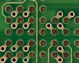
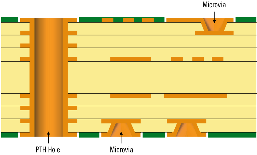
Blind holes, also known as blind vias, are a type of interconnection used in multilayer PCBs. Unlike through-holes that extend through the entire board, blind holes start at one surface of the PCB and terminate at an inner layer, without reaching the opposite side of the board.
Challenges with Traditional Blind Hole Filling Methods
Traditional methods of filling blind holes have several limitations:
- Incomplete filling: Air pockets or voids can form, compromising reliability.
- Uneven surfaces: Filled holes may not be perfectly planar with the board surface.
- Time-consuming processes: Multiple steps are often required, increasing production time.
- Material waste: Excess filling material may need to be removed, leading to waste.
- Limited depth-to-diameter ratios: Traditional methods struggle with high aspect ratio holes.

The Panel-Plating Blind-Hole Filling Method
Principle of Operation
The panel-plating blind-hole filling method is a novel approach that combines the processes of hole filling and surface plating into a single step. This method utilizes a specially formulated conductive material that is applied to the entire panel surface, simultaneously filling the blind holes and creating a conductive layer on the board surface.
Key Components of the Process
- Conductive filling material: A specially designed material that combines properties of both plating and filling.
- Application equipment: Modified plating equipment capable of uniform material application.
- Curing system: Specialized curing process to ensure proper solidification of the filling material.
Step-by-Step Process
- Surface preparation: The PCB panel is cleaned and prepared for the filling process.
- Material application: The conductive filling material is applied uniformly across the entire panel surface.
- Vacuum assistance: A vacuum may be applied to ensure complete penetration of the material into the blind holes.
- Curing: The panel undergoes a controlled curing process to solidify the filling material.
- Surface treatment: The panel surface is planarized to achieve a uniform thickness.
- Final plating: Additional plating may be applied to enhance conductivity and protection.
Advantages of Panel-Plating Blind-Hole Filling
1. Improved Filling Quality
The panel-plating method ensures more complete and uniform filling of blind holes, reducing the risk of voids and air pockets.
2. Enhanced Planarity
By applying the filling material across the entire panel, this method achieves better surface planarity, crucial for subsequent processing steps.
3. Increased Production Efficiency
Combining filling and plating into a single step significantly reduces processing time and simplifies the manufacturing process.
4. Material Savings
The precise application of filling material reduces waste compared to traditional methods that may require excess material removal.
5. Higher Aspect Ratio Capability
This method allows for the filling of blind holes with higher depth-to-diameter ratios, enabling more compact PCB designs.
6. Improved Reliability
The uniform filling and seamless integration with the surface plating enhance the overall reliability of the PCB interconnections.
Comparison with Traditional Blind-Hole Filling Methods
| Aspect | Traditional Methods | Panel-Plating Method |
| Process Steps | Multiple separate steps | Combined filling and plating |
| Filling Quality | Potential for voids | Improved uniformity |
| Surface Planarity | May require additional processing | Better inherent planarity |
| Production Time | Longer due to multiple steps | Shorter, more efficient process |
| Material Waste | Higher, due to overfill and removal | Lower, more precise application |
| Aspect Ratio Capability | Limited | Higher aspect ratios possible |
| Reliability | Good, but dependent on filling quality | Improved due to better filling and |
Applications and Impact on PCB Design
Suitable Applications
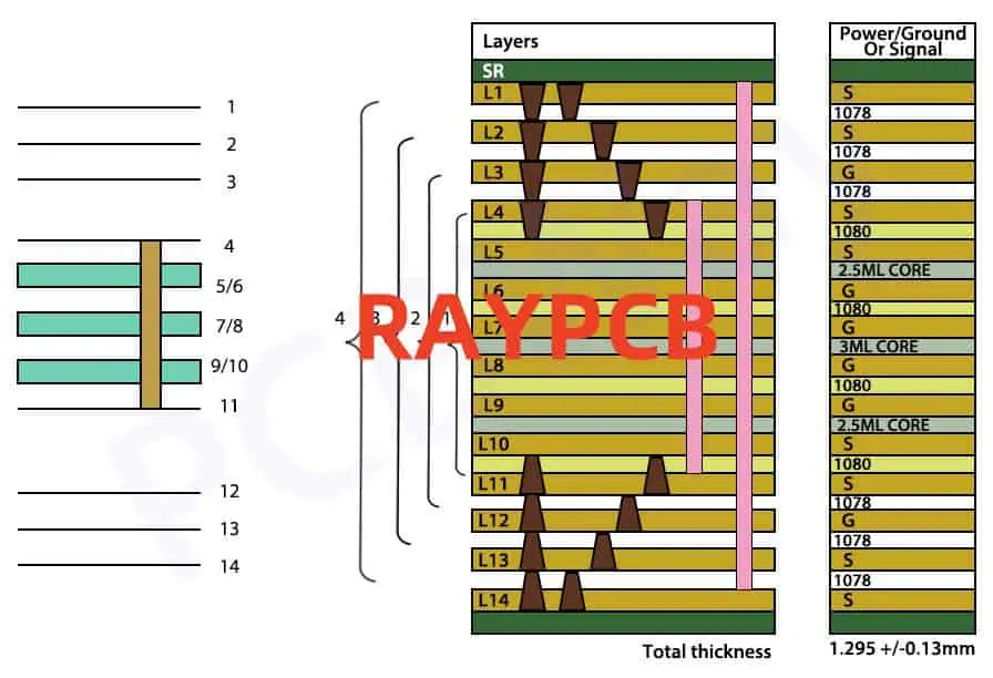
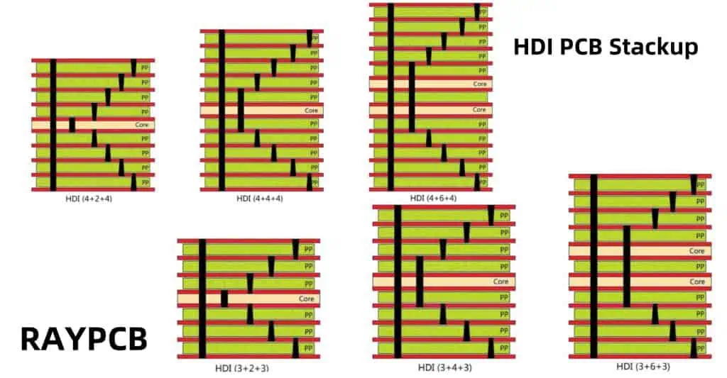
- High-density interconnect (HDI) boards: Ideal for compact designs with multiple layers.
- High-frequency applications: Improved filling quality benefits signal integrity.
- Automotive and aerospace electronics: Enhanced reliability for demanding environments.
- Medical devices: Suitable for miniaturized, high-reliability applications.
Impact on PCB Design Possibilities
- Increased layer count: Enables more complex multilayer designs.
- Finer pitch components: Supports the use of components with tighter lead spacing.
- Improved signal routing: Allows for more efficient use of board real estate.
- Enhanced thermal management: Better filling can improve heat dissipation in power applications.
Challenges and Considerations
1. Material Development
The success of this method heavily relies on the properties of the conductive filling material. Ongoing research is needed to optimize:
- Viscosity for proper hole filling
- Conductivity for electrical performance
- Thermal stability for reliability
- Adhesion to various substrate materials
2. Equipment Adaptation
Existing PCB manufacturing equipment may need modifications to accommodate the panel-plating process, potentially requiring significant investment.
3. Process Control
Maintaining consistent results across large panels and different hole sizes requires precise control of:
- Material application thickness
- Curing parameters
- Surface planarization
4. Compatibility with Existing Standards
The adoption of this new method may require updates to industry standards and certification processes.
5. Cost Considerations
While the method promises increased efficiency, initial implementation costs may be high due to new materials and equipment requirements.
Future Developments and Research Directions
1. Material Innovations
Research into advanced conductive polymers and nanocomposites could lead to filling materials with enhanced properties, such as:
- Higher conductivity
- Improved thermal management
- Better mechanical stability
- Environmental friendliness
2. Process Automation
Development of fully automated systems for panel-plating blind-hole filling could further improve efficiency and consistency.
3. Integration with Additive Manufacturing
Exploring ways to combine panel-plating blind-hole filling with additive PCB manufacturing techniques could lead to novel fabrication methods.
4. Miniaturization
Pushing the limits of hole sizes and aspect ratios that can be reliably filled using this method to support ongoing miniaturization trends in electronics.
5. Hybrid Materials
Investigation into materials that can serve multiple functions, such as combining structural support with electrical conductivity.
Industry Adoption and Standardization
Current Status of Adoption
As a relatively new technology, panel-plating blind-hole filling is still in the early stages of industry adoption. Several factors influencing its uptake include:
- Proven reliability in real-world applications
- Cost-effectiveness compared to traditional methods
- Compatibility with existing PCB design and manufacturing workflows
Steps Towards Standardization
For widespread adoption, the following steps towards standardization are crucial:
- Industry collaboration: PCB manufacturers, material suppliers, and equipment makers working together to refine the process.
- Performance benchmarking: Establishing standard tests to compare the performance of panel-plated blind holes with traditional methods.
- Documentation and guidelines: Creating comprehensive documentation and best practices for implementing the new method.
- Training and education: Developing programs to train PCB designers and manufacturers in the new technique.
Potential Impact on PCB Manufacturing Industry
The successful adoption of panel-plating blind-hole filling could lead to:
- Shift in manufacturing processes: Potentially replacing some traditional plating and filling steps.
- New material supply chains: Creating demand for specialized conductive filling materials.
- Equipment market changes: Driving innovation in PCB manufacturing equipment.
- Design software updates: CAD tools may need updates to account for the new manufacturing capabilities.
Environmental and Sustainability Considerations
Potential Environmental Benefits
- Reduced material waste: More efficient use of filling and plating materials.
- Lower energy consumption: Combining steps may lead to overall energy savings in the manufacturing process.
- Potential for eco-friendly materials: Development of bio-based or more easily recyclable filling compounds.
Sustainability Challenges
- Material recyclability: Ensuring that PCBs manufactured with this method can be effectively recycled at end-of-life.
- Chemical use: Evaluating and minimizing any harmful chemicals used in the filling material or process.
Conclusion
The panel-plating blind-hole filling method represents a significant innovation in PCB manufacturing technology. By combining the processes of hole filling and surface plating, it offers the potential for improved efficiency, reliability, and design possibilities in multilayer PCB production. While challenges remain in terms of material development, process control, and industry adoption, the benefits of this method make it a promising avenue for future development in PCB manufacturing.
As the electronics industry continues to demand more compact, complex, and reliable PCBs, innovations like panel-plating blind-hole filling will play a crucial role in meeting these needs. The success of this method will depend on ongoing research, industry collaboration, and careful consideration of both technical and environmental factors. As it matures, panel-plating blind-hole filling has the potential to become a standard process in advanced PCB manufacturing, enabling the next generation of electronic devices across various industries.
Frequently Asked Questions (FAQ)
1. How does panel-plating blind-hole filling compare to electrolytic copper plating for blind vias?
Panel-plating blind-hole filling offers several advantages over traditional electrolytic copper plating:
- It combines filling and plating in one step, increasing efficiency.
- It typically achieves better planarity and more complete filling.
- It can handle higher aspect ratio holes more effectively.
However, electrolytic copper plating is a well-established process with known reliability. The choice between methods depends on specific application requirements and manufacturing capabilities.
2. Can panel-plating blind-hole filling be used for all types of PCB materials?
While panel-plating blind-hole filling is versatile, its effectiveness can vary depending on the PCB material. It works well with common FR-4 substrates, but special considerations may be needed for:
- High-frequency materials
- Flexible PCB substrates
- Ceramic-based PCBs
Material compatibility should be verified through testing for each specific application.
3. What are the limitations on hole size and aspect ratio for this method?
The exact limitations depend on the specific materials and equipment used, but generally:
- Minimum hole diameter: Currently achievable down to about 50-75 microns
- Maximum aspect ratio: Typically up to 10:1, with some advanced systems claiming higher ratios
These parameters are continually improving as the technology develops.
4. How does this method affect the electrical properties of the PCB?
Panel-plating blind-hole filling can potentially improve electrical properties by:
- Ensuring more consistent conductor thickness in the holes
- Reducing signal reflections due to better hole filling
- Improving overall impedance control
However, the specific electrical performance depends on the properties of the filling material used and the quality of the process control.
5. Is panel-plating blind-hole filling compatible with existing PCB design rules?
While panel-plating blind-hole filling can often work within existing design rules, it may allow for some modifications:
- Potentially smaller via sizes
- Higher aspect ratio holes
- Closer spacing of vias
Designers should consult with manufacturers to understand the specific capabilities and limitations when using this method, as some adjustments to design rules may be beneficial to fully leverage its advantages.