X7R vs C0G ceramic capacitors — learn the real electrical differences, DC bias derating risks, and exactly which dielectric to use for your PCB application.
If you’ve spent any time selecting capacitors for a PCB design, you’ve almost certainly stared at a datasheet wondering whether to grab an X7R or a C0G. They’re both ceramic capacitors, they look identical on the reel, and a junior engineer swapping one for the other can silently break a design without a single error message. This guide walks through the real-world differences from a PCB design perspective — what these codes actually mean, where each dielectric shines, and where it will let you down.
What Do X7R and C0G Actually Mean?
Before diving into the comparison, it helps to understand the naming system. Both X7R and C0G follow the EIA RS-198 standard for ceramic capacitor dielectrics.
Decoding the C0G Code
C0G is a Class 1 dielectric. The code breaks down like this:
- C = significant figure of temperature coefficient: 0 (zero)
- 0 = multiplier: ×1 (so 0 × 1 = 0 ppm/°C)
- G = tolerance on the temperature coefficient: ±30 ppm/°C
The result: a capacitor whose capacitance shifts by 0 ±30 ppm/°C across temperature. Over the full -55°C to +125°C range, that’s less than ±0.3% change in capacitance. C0G is also called NP0 (Negative-Positive-Zero) in military and European standards — same component, different label. Both the “0” in C0G and the “0” in NP0 are the numeral zero, not the letter O.
Decoding the X7R Code
X7R is a Class 2 dielectric. The code breaks down differently:
- X = lower operating temperature: -55°C
- 7 = upper operating temperature: +125°C
- R = maximum capacitance change: ±15%
So across -55°C to +125°C, an X7R capacitor can drift up to ±15% from its nominal value. That sounds manageable, but there’s more to the story — temperature is only one of the variables you have to worry about.
X7R vs C0G: Side-by-Side Comparison
| Property | C0G (NP0) | X7R |
| Dielectric Class | Class 1 | Class 2 |
| Temperature Range | -55°C to +125°C | -55°C to +125°C |
| Capacitance Change vs. Temp | 0 ±30 ppm/°C (< ±0.3%) | ±15% max |
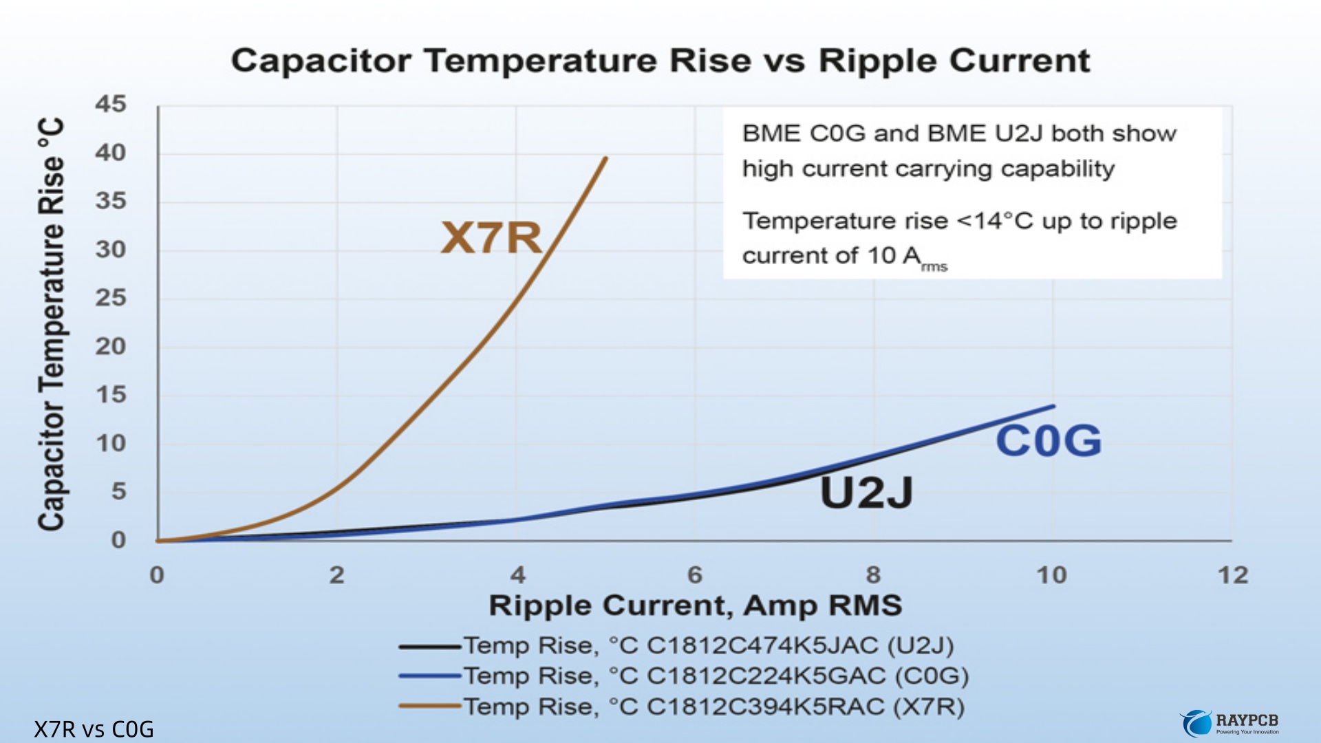
| DC Bias Effect | None | Significant — can lose 50–80% |
| Aging | Negligible | ~1% per decade |
| Piezoelectric Effect | None | Yes (microphonics) |
| Typical Max Capacitance | ~10 nF to 100 nF (per case size) | Up to 47 µF |
| Typical Tolerance | ±1%, ±2%, ±5% | ±10%, ±20% |
| Relative Cost | Higher | Lower |
| Package Size for Same Value | Larger | Smaller |
| Dielectric Absorption | < 0.6% | Higher |
| Q Factor | >1000 | Lower |
| Best For | Precision, RF, timing | Decoupling, bulk bypass |
The Hidden X7R Problem: DC Bias Derating
This is the one that catches engineers off guard, especially those coming from simulation backgrounds. Class 2 capacitors lose capacitance as you apply DC voltage. This is not a small effect.
A 10 µF X7R capacitor rated at 16V can behave like a 2 µF capacitor when 12V is applied across it. The ferroelectric dielectric in X7R responds to the electric field, and its effective permittivity drops — taking your capacitance with it. Some manufacturers’ datasheets show derating curves that drop 70% or more at rated voltage.
The practical takeaway: if you’re using an X7R capacitor in a power rail decoupling application, always check the manufacturer’s DC bias derating curve and derate accordingly. A rule of thumb many engineers use is to select a voltage rating at least twice the actual operating voltage to stay in the flat portion of the derating curve. C0G capacitors have no measurable DC bias effect — what you see on the datasheet is what you get in the circuit.
Capacitance Stability: Where C0G Has No Competition
For any application where the capacitor value must stay predictable, C0G is the clear choice. Here’s why the ±30 ppm/°C number is genuinely impressive:
Over the full -55°C to +125°C range (a 180°C swing), the capacitance changes by just ±0.54%. Capacitance drift and hysteresis are below ±0.05%. Dielectric absorption is less than 0.6% — comparable to mica capacitors, which have been the gold standard for precision applications for decades. The Q factor for C0G routinely exceeds 1000, making it ideal at RF frequencies.
X7R capacitance, by contrast, follows a nonlinear curve with temperature, shifts with applied voltage, and ages over time — losing roughly 1% per decade, or about 5% over 10 years. None of these effects are disqualifying for the right application. But in precision timing, filtering, or RF circuits, they add up fast.
When to Use C0G: Application Checklist
C0G is the right call when the capacitor value directly affects circuit performance.
Timing and Oscillator Circuits
Any RC timing network, crystal oscillator load capacitor, or ceramic resonator application needs a stable C value. A ±15% drift in an X7R timing capacitor means your oscillator frequency shifts with temperature. Use C0G.
RF Tuning and Matching Networks
At radio frequencies, capacitor Q and stability are critical. C0G’s high Q (>1000) and predictable temperature behavior make it the standard for RF tuning, impedance matching, and tank circuits in LNA and VCO designs.
Active Filters with Precision Frequency Response
Sallen-Key, multiple feedback, and other active filter topologies rely on accurate capacitor ratios to set pole frequency and Q. X7R will shift your cutoff frequency across temperature. C0G holds the filter response tight.
High-Impedance Analog Nodes
Precision ADC input networks, sample-and-hold circuits, and op-amp feedback networks benefit from C0G’s negligible dielectric absorption. High dielectric absorption causes charge retention errors that show up as settling time issues in high-resolution converters.
Low-Noise Sensitive Circuits
X7R capacitors exhibit piezoelectric behavior — mechanical vibration causes voltage noise. In audio circuits, precision instrumentation, and low-noise analog front ends, this “microphonics” effect can inject µV-level noise. C0G is not piezoelectric and is immune to this.
When to Use X7R: Application Checklist
X7R is not a second-choice dielectric — it’s the right tool for high-value bypass and decoupling applications.
Power Supply Decoupling
The bulk of MLCC decoupling on a modern PCB is X7R. You need large capacitance values in small packages, and X7R delivers. Just derate the voltage rating properly and check the DC bias curve.
Bypass Capacitors on Digital ICs
Digital logic doesn’t care whether its bypass cap is exactly 100 nF or 88 nF. The ±15% temperature drift of X7R has no meaningful effect on the performance of a digital power pin. Use X7R here — it’s smaller, cheaper, and fits the job.
Bulk Input/Output Filtering
Buck converter input capacitors, LDO output capacitors, and EMI filter capacitors all benefit from X7R’s high capacitance density. Use multiple X7R capacitors in parallel and derate their voltage ratings.
Coupling Capacitors (Non-Critical)
Interstage coupling where the exact capacitance value is not critical to gain or frequency response is a perfectly reasonable X7R application. If the coupling cap just needs to block DC and you have bandwidth to spare, X7R works fine.
X7R vs C0G: Application Decision Table
| Application | Recommended Dielectric | Reason |
| Crystal oscillator load caps | C0G | Frequency stability |
| RF tank / tuning circuits | C0G | High Q, stable |
| Active filter (precision) | C0G | Stable pole frequency |
| Sample and hold | C0G | Low dielectric absorption |
| Low-noise analog (microphonics concern) | C0G | Non-piezoelectric |
| Power supply bypass (bulk) | X7R | High capacitance density |
| Digital IC decoupling | X7R | Cost/size efficient |
| Buck converter input cap | X7R (derated) | High bulk capacitance |
| LDO output cap | X7R | High value in small package |
| Non-critical AC coupling | X7R | Adequate stability |
| High-temperature (>150°C) | C0G (special grade) | X7R degrades severely |
Package Size Realities
One practical constraint engineers run into is that C0G capacitors top out at much lower capacitance values for a given package size. If you search a distributor for a 0.1 µF 0805 ceramic capacitor, you’ll find hundreds of X7R results and virtually zero C0G options. For 100 nF and above, X7R is often the only practical MLCC option in standard package sizes.
This is a materials limitation: the high-permittivity ferroelectric dielectric in X7R can pack far more capacitance into the same volume. C0G is fundamentally limited by its lower dielectric constant (below 150 for TiO2-based formulations), while X7R dielectric constants can exceed 2000.
For low-value capacitors — anything from 1 pF to a few nanofarads — C0G is readily available in standard 0402 and 0603 packages and is the preferred choice whenever stability matters.
A Note on Identifying Them in the Field
This comes up in manufacturing and rework. Both C0G and X7R MLCCs can look physically identical once they’re off the tape. A common industry observation is that C0G caps tend to have a grey color while X7R parts are more brown — but this is manufacturer-dependent and should never be relied upon for positive identification. Always cross-reference the part number against the manufacturer datasheet. Swapping an X7R for a C0G may work fine, but swapping a C0G for an X7R in a precision circuit can introduce subtle failures that are very hard to debug.
Frequently Asked Questions
Q1: Can I substitute C0G for X7R in a decoupling application?
Yes, in most cases. C0G will perform at least as well as X7R for bypass and decoupling. The only practical issue is that you may not find C0G options in the large capacitance values (1 µF and above) needed for bulk decoupling, and C0G parts cost more. For small-value bypass caps, C0G is a perfectly fine substitute.
Q2: Can I substitute X7R for C0G in a timing or filter circuit?
Generally no, and this is where designs get into trouble. The ±15% capacitance variation with temperature, plus DC bias derating and aging, can shift timing and filter frequencies enough to cause circuit failures. Unless you’ve verified the tolerance is acceptable for your design, stick with C0G for precision applications.
Q3: Why does an X7R capacitor measure much lower than rated capacitance on my bench LCR meter?
Your LCR meter may be applying a test voltage, and X7R capacitance drops significantly under DC bias. Also, X7R capacitance changes with the AC measurement signal frequency and amplitude. Measure at the actual operating conditions when possible, or consult the manufacturer’s derating curves.
Q4: What is the difference between C0G and NP0?
They are the same capacitor specified under two different standards. C0G is the EIA designation (used predominantly in North America). NP0 (Negative-Positive-Zero) is used in military standards and commonly seen in European documentation. The “0” in both designations is the numeral zero, though it is frequently written as the letter O, especially as “NPO.”
Q5: Do X7R capacitors really make noise in audio circuits?
Yes. X7R and other Class 2 ceramics are ferroelectric and exhibit piezoelectric behavior. Board vibrations (from fans, motors, or speakers) can physically flex the capacitor, generating a small voltage. In sensitive audio circuits, this appears as audible noise or hum. C0G is not piezoelectric, which is one reason it’s preferred in precision analog and audio reference circuits.
Useful Resources
| Resource | Description | Link |
| Murata SimSurfing | Simulate capacitor behavior under DC bias, frequency, and temperature | murata.com |
| KEMET KSIM | KEMET’s capacitor simulation tool with derating curves | ksim3.kemet.com |
| TDK Product Selector | Search TDK MLCC by dielectric, capacitance, voltage | product.tdk.com |
| AVX (Kyocera) Parametric Search | Filter by C0G or X7R, size, voltage | avx.com |
| Digi-Key MLCC Filter | Distributor search with dielectric filter | digikey.com |
| EIA RS-198 Standard Summary | Background on EIA ceramic capacitor classification | Available via IHS Markit |
| TI Precision Hub — Microphonics Series | Detailed explanation of piezoelectric noise in MLCCs | e2e.ti.com |
Summary
The X7R vs C0G decision comes down to one question: does the capacitor value matter to your circuit’s performance?
If you need stability — for timing, filtering, RF tuning, or precision analog — C0G is the answer. Its temperature stability (0 ±30 ppm/°C), zero DC bias effect, high Q, non-piezoelectric behavior, and negligible aging make it the reference-grade dielectric for work where accuracy matters. The trade-off is cost and limited availability at high capacitance values.
If you need bulk capacitance in a tight space for power decoupling, bypass, or non-critical coupling — X7R is the right tool. It’s cost-effective, widely available in values up to 47 µF, and entirely adequate when the exact capacitor value is not critical to the function. Just derate the voltage rating and check the DC bias curve before committing to a value.
Most PCBs need both. Use C0G at precision analog nodes, oscillator pins, and RF sections. Use X7R everywhere else.