MAPS-010164-TR0500: A 6-Bit Digital Phase Shifter for Surface-Mount Devices

MAPS-010164-TR0500

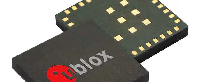
Surface-mount devices are those devices designed and optimized with the Surface Mount Technology (SMT). Therefore, the popularity is mostly because of the simplicity. Now, several design iterations have been developed to work alongside these Surface Mount Technology. Digital phase shifting is one of such concepts.

In todayโ€™s blog post, we will look at MAPS-010164-TR0500, a 6-bit digital phase shifter. You will understand how a digital phase shifter works, how the MAPS-010164-TR0500 makes all the difference and the benefits to the surface-mount devices.

What is Digital Phase Shifter?

It basically has to do with โ€œshifting the phaseโ€ right? That is the โ€œsurface meaning.โ€ According to everythingRF, digital phase shifters are those โ€œdevices that are used to change the phase of an RF signal digitally while keeping its amplitude constant.โ€

The question therefore is โ€œwhat is the importance of shifting the RF signals?โ€ The major reason why these signals are to be shifted is because of the need to streamline and maximize wireless transmission of information.

You can rely on MAPS-010164-TR0500 to do that โ€“ and much more.

Having that in mind, we are now going to go in-depth into the core attributes of this digital phase shifter.

MAPS-010164-TR0500 Minimizes Attenuation

Although the goal is to streamline wireless data or information transmission, MAPS-010164-TR0500 also takes note not to exceed it. That is while it maintains the most minimized attenuation rate.

As per the information in the datasheet, it can provide a phase shift from 0หš to 360หš in 5.6หš steps.

MAPS-010164-TR0500 Supports Dual Control Methods

FULL PCB MANUFACTURING Quote

Controlling the processes of shifting the phase on MAPS-010164-TR0500 doesnโ€™t take much effort. This digital phase shifter offers excellent control, through the dual-control options.

These options are:

1. Direct Parallel Mode

This mode or control option ideally offers a โ€œdirect parallelismโ€ for the digital phase shifter to be controlled.

However, the direct parallel mode is subject to working under some conditions. It becomes active or functional after the P/S is set low.

Once the P/S is set low, the D1, D2, and the D3 function would be controlled by the Pins 22, 23 and 24.

For maximum performance, the direct parallel mode has to be controlled by the parallel control inputs.

2. Serial Mode

This is the opposite of the direct parallel mode, in the sense that it becomes active after the P/S is set high.

It is also compatible with the serial control interfaces: SEROUT, SERIN, LE and CLK.

The serial mode also performs a wide range of other relevant functions, including:

Data Protection

Since digital phase shifters focus on the excellent transmission of data/information wirelessly, it is also imperative to protect the same.

That is what MAPS-010164-TR0500โ€™s serial mode offers by delegating the CLK serial control interface to protect or mask the transmitted data when the LE interface is high.

Desired Phase Shifting

Shifting the digital phase accurately is also enabled through the loading of the 6-bit serial word with the MSB first.

Then, after the 6-bit word has been shifted, there will be a rising edge on the LE serial control interface. The edge now helps in setting the phase shifter to the desired state.

Overall Coverage

Digital phase shifting should be done in a way that it covers most parts of the target device. MAPS-010164-TR0500 offers that through the support for a 360หš coverage with the LSB equaling 5.6หš.

Low-Power

Despite the various phase shifting methods, MAPS-010164-TR0500 doesnโ€™t consume excessive power. It uses a low DC power to conserve power usage.
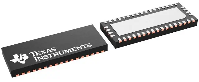
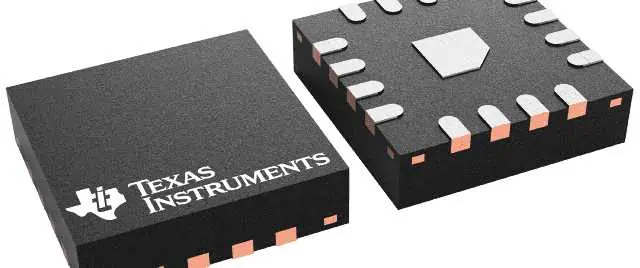
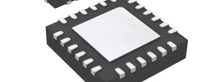
Pin Configuration

MAPS-010164-TR0500 supports up to 24 pins, but these pins are to be used based on the functions. For example, the 24-pin configuration is used with the D1 or the SER IN, while the 3-pin configuration is ideal for GND.

Note that for the pins to function accurately, they need to be correlated to the exposed pad. To that end, the exposed pad is to be positioned at the packageโ€™s bottom and must be connected to both the DC ground and the RF to function effectively.

Typical Applications

The best types of applications or devices to use with the MAPS-010164-TR0500 are those that require a higher minimum loss variation over the shift range.

MAPS-010164-TR0500โ€™s minimal attenuation variation over phase shift range fits into that description.

You also want to use this 6-bit digital phase shifter with devices that require a smaller footprint. In that case, the 4 mm PQFN package offered by MAPS-010164-TR0500 is an ideal small form-factor package for those devices.

Examples of the devices that have been configured with the MAPS-010164-TR0500 are:

  • Phased array radars
  • Communications antennas

What to Look for when Choosing a Digital Phase Shifter

The shifter can change the RF signalโ€™s phase and facilitate real-time, accurate data transmission. Yet, you want to be intentional when choosing one. Here are some tips to guide you:

What is the Minimum Phase Shift Step?

Digital phase shifting is counted in โ€œsteps.โ€ In MAPS-010164-TR0500โ€™s case, it can shift from the 0หš to 360หš in 5.6หš steps.

The minimum phase shift step tells you how long it may take to make the phase shift. It is generally known as โ€œLeast Significant Bit or LSB.โ€

Check the Phase Shift

Check the phase shift, which is usually represented in degrees (หš). It is the range of the shift made and is controlled by the digital control logic.

Frequency

What is the frequency at which the digital phase shifter makes or provides the needed phase shift?

How Many Bits Does the Digital Phase Shifter have?

MAPS-010164-TR0500 has 6 bits, but is there a need for more bits? The bits in this case, refer to the number of โ€œitemsโ€ (bits) that can be used in controlling the phase shift.

The goal is to go for a digital phase shifter that has a higher number of bits, because that can increase the phase shifterโ€™s resolution. The โ€œresolutionโ€ in this case, refers to the smaller increment in each phase.

Final Words

MAPS-010164-TR0500โ€™s 6-bit digital phase shifter provides an amplitude change, while changing the phase of the RF and the millimeter of the wave signals

TPS76801MPWPREP: A Linear Voltage Regulator with Fast Transient Response

TPS76801MPWPREP

Voltage regulators are one of the core Power Management ICs (PMICs) used with many consumer electronics. These regulators work by enabling a real-time regulation of the power or current transmission to and from the target applications.

Now, there are different variants of these regulators and the linear voltage regulators are one of such. In this article, we discuss TPS76801MPWPREP as a linear voltage regulator with a fast transient response capability.

What is a Linear Voltage Regulator?

Generally, voltage regulators help in optimizing how current (power) is to be received and converted to the best performances.

But what is a linear voltage regulator and why does it matter in the scheme of things? Linear voltage regulator is a type of voltage regulator that maintains a fixed output voltage. This maintenance is done by using a controlling circuit to regulate the driver transistorโ€™s resistance.

Wikipedia adds that one of the core features of a linear voltage regulator is the heat dissipation model, which involves dissipating heat across the regulation device. Doing this helps the linear voltage regulator to effectively control the target deviceโ€™s output voltage.

TPS76801MPWPREP is a Low-Dropout Voltage: What Does It Do?

FULL PCB MANUFACTURING Quote

Further breaking it down, TPS76801MPWPREP works as a Low-Dropout Voltage or LDO. According to Texas Instruments, an LDO is a type of voltage that provides a โ€œregulated output voltage that is powered from a higher voltage input.โ€ This is implementable in a variety of applications.

Wikipedia furthers add that a Low-Dropout Voltage (LDO) is a type of Direct Current (DC) linear voltage regulator, capable of regulating the output voltage. The regulation is done, irrespective of whether the supply voltage is closer to the output voltage or not.

The Power Good Feature

Besides regulating the output voltage, the TPS76801MPWPREPโ€™s LDO also helps optimize the regulator for the best power uses. It does this with the Power Good (PG) feature. The feature helps to implement either a low-battery indictor or a power-on reset for the target device.

It has a Controlled Baseline

The controlled baseline used here refers to the one-housed design for how TPS76801MPWPREP operates. Here, we have the likes of one fabrication site and one assembly and test site.

Therefore, everything relating to how TPS76801MPWPREP is to be configured for the best possible results and performances are processed here.

TPS76801MPWPREPโ€™s Response to the pnp Pass Element

The pnp Pass Element is a common feature on most Low-Dropout Voltage Regulators (LDOs). The pnp Pass Element is a โ€œbase currentโ€ proportional to the load current passed through the regulator.

However, there are a couple of design challenges peculiar to the pnp Pass Element. These challenges include:

1. Low-Operating Current

The systemโ€™s operating current is usually low and can sometimes, be invariably over the full load range. That happens when the systemโ€™s pnp Pass Element uses a PMOS Transistor to pass current, rather than using the PMOS gate. The latter (the PMOS gate) could have been used, but wouldnโ€™t because the gate is driven by the voltage.

2. Large Start-Up Currents

The start-up currents are usually higher on devices designed with the pnp Pass Element. It happens because of the following factors:

  • The pnp Pass Element tends to saturate when the device goes into dropout.
  • There is a drop in the รŸ forces. This drop paves the way for an increase in the IB required to maintain the load.

It is therefore, imperative to find a viable way to address that concern. TPS76801MPWPREP perfectly handles that via the very low quiescent current. The amazing thing about this current is that it remains โ€œvirtually constant even when with varying loads.โ€

TPS76801MPWPREP is Stable

TPS76801MPWPREP is designed to be a stable Linear Voltage Regulator, as it is designed to have a fast transient responseย that makes the system stable when working with the 10-ยตF low ESR capacitors.

What You Need to Know about a Low-Dropout (LDO) Voltage

We have ascertained that TPS76801MPWPREP is a Low-Dropout (LDO) voltage and that it can help balance the current transfer within the system.

Now, let us look at some of the additional pieces of information that are sometimes left out about how an LDO works:

3. Power Conversion to Heat

It is the number one function of a Low-Dropout Voltage (LDO) voltage to convert excess power into heat. This conversion is first, a good way to regulate the voltage and a process for making the TPS76801MPWPREP Integrated Circuit (IC) ideal for use with the small-sized and low-power applications.

4. An LDO can Tackle Noise

Noisy operation is tenable in some circuits and it is in the place of the Low-Dropout (LDO) voltage to limit that.

Depending on the design process, it may be worth it to use a High-Power-Supply Rejection Ratio (PSRR) regulator. It works by operating at a higher bandwidth, which paves the way for the LDO to โ€œclose the gap in noiseโ€ by filter the switching noise coming from the upstream DC-to-DC converters.

Choosing and LDO: What to Look for

Naturally, your choice of a Low-Dropout (LDO) voltage that doubles as a linear voltage regulator is along the lines of โ€œhow much does it cost.โ€

While cost is an important consideration, it doesnโ€™t always have to come first-place over other important factors. If you are looking to buy an LDO like TPS76801MPWPREP, these are a few of the things to look for:

5. Power Dissipation Process

How does the LDO handle excessive power? In TPS76801MPWPREPโ€™s case, it does that by spreading or dissipating the excessive power through the conversion into heat.

6. Load Current

How many loads can the LDO carry or support? Pay attention to both the minimum and the maximum load current.

The major thing to consider in this case is the functioning of the LDO after loading. For TPS76801MPWPREP, it remains โ€œvirtually constant even with varying loads.โ€ It also remains stable even at zero load; making it one of the LDOs that function effectively without needing any minimum load for the operation.

Conclusion

TPS76801MPWPREPโ€™s fast transient response is a unique feature that helps the Low-Dropout (LDO) voltage to maintain a regulated output voltage as a response to the sudden changes in the load current.

HIP4082IBZ: A Half-Bridge FET Gate Driver

HIP4082IBZ

HIP4082IBZ is a half-bridge or H-Bridge FET gate driver by Renesas Electronics America Incorporated. The company manufactured this gate driver to drive or increase the performance of circuit boards.

Read this comprehensive article to get an idea of how it works and every other thing in-between.

HIP4082IBZ as a Gate Driver

Gate drivers are a part of the Power Management Integrated Circuits (PMICs). Like the other PMICs, they help to optimize the target device, application or circuit board for the best power usages.

The gate driver also aids the isolation, bootstrapping, amplification and reference shifting capabilities of the target devices.

One thing is outstanding in a gate driverโ€™s performance โ€“ it can function alone, hence, the isolation in most cases. And for a gate driver to make the most out of the performance, if often interfaces or distributes the signals from a control device in a power-converting device to a semiconductor device โ€“ which can either be an IGBT or a FET.

A half-bridge is a type of inverter or gate driver, which helps in driving the gates of the low-side and high-side N-channel MOSFETs. This driver paves the way for a low output impedance to come in and drive the signals from the one part to the other.

This process does not only reduce switching losses due to the fast-switching time, but also reduces the chances of getting conduction-related losses.

The N-Channel MOSFETs Concept

FULL PCB MANUFACTURING Quote

Most half-bridges use an N-channel MOSFET โ€“ but why? As Homemade Circuitsย pointed out, the role of an N-channel MOSFET in a half-bridge is to bridge the gap, following the absence of center top transformers.

To that end, HIP4082IBZโ€™s N-channel helps to improve the performance of the MOSFETs.

However, some challenges are feasible because of the inability to drive the higher or upper sides of the MOSFETs. The main challenge here is the use of 4 channels at the topology; a composition that inhibits the MOSFETโ€™s performance, in the sense that the MOSFETs now have higher loads resistance at the source terminal.

Therefore, it is imperative for the MOSFETs to be freed to function optimally. That necessitated the need for a higher voltage.

HIP4082IBZโ€™s Higher Voltage: What You Need to Know

The need for a higher voltage to drive the MOSFETsโ€™ performance is because of the need to switch the higher topology further. To make that switch, the voltage should be above the available supply voltage.

That informs the reason behind HIP4082IBZโ€™s supply voltage that ranges between 8.5 volts and 15 volts.

Switchable Frequencies

Besides the higher voltage, HIP4082IBZโ€™s half-bridge FET gate driver can also be increased in terms of the operating frequencies. Using the user-programmable dead times ranging between 0.1 to 4.5ยตs.

The broader selections of dead times pave the wave for the onward configuration of the half-bridge to support higher frequency switching up to 200kHz.

Flexible Inputs

HIP4082IBZ also supports a flexible input protocol, which comes in handy for driving every possible combination on the circuit board.

There is an exception though. The combinations that donโ€™t tow this line tend to use the shoot-through protection/condition.

Independent Driver

HIP4082IBZ doubles as a full and half-bridge gate driver, thanks to the independent driver for the N-channel FET. Therefore, you can configure it to work for both the full and the half-bridge applications.

Undervoltage Protection

As much HIP4082IBZ looks to increase the gate driverโ€™s performance, it also takes note not to allow it slip below performance. To that end, it uses an undervoltage protection feature to keep the applications active.

The undervoltage protection protects the target applications from below-the-par performance. The core functions here are the VDD Rising Undervoltage Threshold and the VDD Falling Undervoltage Threshold.

Suitable Applications

The ideal applications to use HIP4082IBZ are the ones dedicated to moderate power level usage. On its part, HIP4082IBZ uses an 80-volt operating capacity to facilitate the following applications:

  • Peripherals
  • UPS systems
  • Switching power amplifiers
  • DC motor controls
  • Battery powered vehicles
  • Full bridge power supplies
  • Noise cancellation systems
  • Medium and large voice coil motors

Technical Attributes

Below is a tabular representation of the attributes or specifications for the HIP4082IBZ half-bridge FET gate driver:

AttributesDescription
Operating Temperature (minimum to maximum)Between -55หšC and 150หšC
Driverโ€™s ConfigurationHalf-Bridge
Typical Rise and Fall Time9ns, 9ns
Type of ChannelIndependent
Type of InputNon-Inverting
Type of Gate DriverN-Channel MOSFET
Type of Mounting StyleSurface Mount Technology (SMT)
Number of Gate Drivers4
Maximum High Side Voltage95 volts
Voltage โ€“ SupplyBetween 8.5 volts and 15 volts

HIP4082IBZโ€™s Non-Inverting Input

HIP4082IBZ uses a non-inverting input. We want to explain how it works. According to StackExchange, the non-inverting input has to do with the relationship or the connection between the input and the output levels of the gate driver.

At the basis is the need to establish the right connection and balance the same. Therefore, the non-inverting input works by giving a higher output when a logic high is applied to the input. When this happens, an output low is derived from the low input.

When compared to the inverting input, the non-inverting input works by connecting the logic high to the input to get an output high, while the inverting input works by using a low input to set an output high.

Conclusion

HIP4082IBZโ€™s gate driver performs a similar function as many other gate drivers โ€“ which is the acceptance of a lower power input and producing a corresponding higher current gate drive for the target device.

However, the role of the gate driver becomes prominent following the PWM controllerโ€™s inability to provide the required output current. In the absence of this current, it wouldnโ€™t be possible to drive the required gate capacitance of the targeted device or application.

To that end, using a gate driver like HIP4082IBZ can make all the difference. It first isolates or restricts the gate of the power device so it can take in the charged gate input capacitance. When that is done, the power device turns on only after the required gate threshold voltage is reached.

HD3SS3412RUAR: A Special-Purpose Differential Switch

HD3SS3412RUAR

Texas Instruments manufactured HD3SS3412RUAR as an analog differential switch for special-purpose devices, especially PCIe devices.

In this article, you will learn about this differential switchโ€™s capabilities.

How Does a Differential Switch Work?

A differential switch is also called the differential pressure switch. It works by noticing the pressure or voltage differences between the two points in a system; in this case, a circuit board.

Once the pressure or voltage differences are noticed, the switch helps to balance the differences by switching to the channel that follows the predefined value.

Now, HD3SS3412RUAR works in a similar way, especially with the use of a high-speed switch capable of switching up to four (4) differential channels. That way, it can help these multiple channels to establish multi-connections.

The Analog Switching Capability

HD3SS3412RUAR is an analog switch for special-purposes. What this means is that it doesnโ€™t always tow the path of conventional (general-purpose analog switches), which serve all purposes.

Due to the special designation, HD3SS3412RUARโ€™s analog switch with special-purpose uses is ideal for routing signals via a dedicated Solid State Device (SSD). The routing also includes provisions for special features and functionalities that are hitherto, missing on the general-purpose analog differential switches.

Multiple Switching Capabilities

FULL PCB MANUFACTURING Quote

HD3SS3412RUAR supports the switching of purposes across multiple paths. For example, using the high-speed passive switch capable, the switch can support the following:

  • Four (4) differential channels
  • Support for two full PCI Express (PCIe) x1 lanes from one source to up to 2 target locations inside a server application or PC.
  • It also supports applications that enable connections between multiple source devices. An example of this types of devices is a shared peripheral between two platforms.

Multi-Interface Support

Interfaces play a role in the connections established with a differential switch. HD3SS3412RUARโ€™s supports multiple interface standards.

Common Package Footprint

HD3SS3412RUAR is one of the ideal differential switches for circuit boards and consumer electronics with limited space.

It is because of the common package footprint, optimized into the small 3.5-mm x 9.0-mm, 42-pin WQFN package.

This package is also available in a common footprint, shareable among many vendors.

Excellent Signal Conduction

Conducting the signals from one channel to the other might not always be simple. Therefore, using a mechanism to regulate that is very essential. That is the reason for integrating a Single Control Line (SEL pin) inside HD3SS3412RUAR. This pin aids the control and conduction of signals from one path or channel to the other. It can also be used to conduct the signals backwards.

Full Temperature Operation

HD3SS3412RUAR also supports the temperature use from a single supply voltage of 3.3 volts up to a full operating temperature of 85หšC.

Technical Attributes

The table below represents the technical attributes of this differential switch:

AttributesDescription
Mounting StyleSurface Mount Technology (SMT)
Typical ApplicationPCI Express (PCIe)
Core FeatureBi-Directional
Number of Channels4
Package/Case42-WFQFN Exposed Pad
Operating Temperature (minimum to maximum)Between 0หšC and 70หšC
Multiplexer/Demultiplexer Circuit2:1
-3db Bandwidth8GHz
On-State Resistance (Maximum)80hm
Voltage โ€“ Supply, Single (V+)Between 3 volts and 3.6 volts

HD3SS3412RUAR Application Considerations

HD3SS3412RUAR is ideal for the PCI Express (PCIe) Gen III applications; examples being the following:

  • Shared I/O Ports
  • Desktops and notebooks PCs
  • PCI Express (PCIe) backplanes
  • Storage area networks and servers

However, there are more applications or use cases for this differential switch. It can also be used with other high-speed data protocols, especially if those protocols have up to <1800 mVpp of differential amplitude and a common-mode voltage of <2.0 volts.

It also supports the DisplayPort 1.2 and the USB 3.0 applications.

AC Coupling Caps Consideration

Considerations are also to be made for the AC Coupling Caps. HD3SS3412RUARโ€™s optimization for this is to offer the 0603 capacitors and the 0402 capacitors.

You must avoid using the C-packs or the 0805 size capacitors, but stick to the above.

With that being said, optimizing the capacitors involves setting and matching the value of the 0.1 ยตF capacitor with the ยฑ signal pair.

To ensure a symmetric placement of the AC Coupling Capacitors (Caps), it is better to do that along the TX pairs. Do that by placing the caps on the top-routed TX pairs on the system board.

Although the above is one of the best ways to place the capacitors, there are a number of other options worth exploring. See them below:

1. Coupling the Capacitors on the Both Sides of the Switch

The AC Coupling Capacitors can be placed on both sides of the HD3SS3412RUAR differential switch.

Doing this is required only when the common-mode voltage on the system board is above 2 volts.

As a way of balancing the performance, the less than 2-volts biasing voltage is to be used alongside the common-mode voltage.

2. Capacitorsโ€™ Placement between the Switch TX and the Endpoint TX

HD3SS3412RUARโ€™s AC Coupling Capacitors can also be placed between the switch and the endpoint TXs.

The placement has to be balanced with the biasing of the switch by either the host controller or the system.

3. Placement on the Host and Endpoint Transmit Pairs

This is the third configuration option for HD3SS3412RUARโ€™s differential switchโ€™s capacitors. In this case, the AC Coupling Capacitors are placed on both the host transmit pair and, on the endpoint, transmit pair.

The performance is further balanced with the biasing of the lower switch with the host controller and that of the upper switch by the endpoint.

Concluding Thoughts on HD3SS3412RUAR

HD3SS3412RUAR is a high-performance differential switch, capable of switching the performances and signal transmission across 4 channels. With the bi-directional (MUX/De-MUX) type of differential switch, it facilitates the routing or transmission of high-speed signals between two locations on a circuit board.

However, note that the HD3SS3412RUAR is optimized for special-purpose differential switching applications, most especially the PCI Express Gen III applications. Also, you can use it to route or switch signals in a couple of selected high-speed data protocols and applications. Other than that, it is not to be used with any other (unsupported) application.

Lastly, take note to use the accurate AC Coupling Capacitorsโ€™ placement so you donโ€™t distort the signal routing process.

FT232RQ: A USB to UART Serial Interface

FT232RQ

Not all interfaces work solo or independently in an Integrated Circuit (IC). Some would need additional connections in the form of a bridge to work. That aptly describes, FT232RQ a bridge connecting the Universal Serial Bus (USB) to a UART.

In this article, you will discover some of the important facts about this Integrated Circuit, cum controller.

FT232RQ as a Controller

FT232RQ is an interface classified under Integrated Circuits (ICs). Like most interfaces, it relies on the interface components to establish a connection to the various signals in a circuit board. Through these components, the interface can also transmit or transfer data or bitstream effectively.

When it comes to picking an IC-interface, the options are narrowed down to the closest functional parts. The varieties of interfaces include controllers (an example being FT232RQ), serializers, decoders and encoders. Others are splitters, capacitive touch, Universal Asynchronous Receivers and Transmitters (UARTs), Direct Digital Synthesis (DDS), signal buffers and filters.

To that end, FT232RQ fits into the category by the design as a controller. But how does a controller-based interface work?

It works by providing the โ€œinformatic connectivityโ€ between the endpoints that comprise differing signaling methods and communication protocols.

In addition to establishing the individualized communication endpoints for these devices, the FT232RQ also supports multi-way connections.

The Bridging Perspective

FULL PCB MANUFACTURING Quote

When interfaces are referred to as โ€œbridges,โ€ it simply means that they are used as a pathway for connecting one or more interfaces.

In FT232RQโ€™s instance, it doubles as a bridge and a USB to UART interface. This function allows this controller to connect the Universal Serial Bus (USB) to a serial UART interface.

At the core of this connection are the following benefits:

1. Integrated Clock Generation

In addition to supporting USB to UART interface connection, FT232RQ also supports the minimization of friction during the connection.

As a way of preventing glue-less interfacing to the external Field Programmable Gate Array (FPGA) and Microcontroller (MCU), it supports the full integration of the clock generation. That way, there wouldnโ€™t be any need for an external crystal nor an optional clock output selector.

2. Chip-Based USB Protocol

Just like the clocking peripherals are not externally added, so does the USB protocol for FT232RQ.

Since the entire USB protocol is embedded into a chip, there is no need for an external USB-specific firmware programmer to be used alongside it.

3. Buffer Distribution

Besides being an interface cum bridge for USB to UART interfacing, FT232RQ also enables higher throughputs for the data transmitted through the interface.

The high data throughput is enabled via the FIFOโ€™s reception and transmission of buffers to attain the highest data distribution speed.

Also, it supports the use of a single-chip Universal Serial Bus (USB) to enable the asynchronous serial data transfer.

The potential to get the most of data transmission rates is also evident in the use of the 12 byte receiver buffer and the 256 byte transmit buffer. This combined byte buffers also use the buffer smoothing technologyย to facilitate the transfer of data at a higher speed.

At an estimate, FT232RQโ€™s data transfer speed or rate can move from 300 Maud up to 3 Mbaud when operating at the TTL levels.

Technical Specifications

Below are the tabulated attributes of FT232RQโ€™s USB to UART serial interface:

Product AttributesDescription
Operating Temperature (minimum to maximum)Between 40หšC and 85หšC
Protocol UsedUniversal Serial Bus (USB)
Current (supply)15mA
Core FunctionsUSB to UART interface and a Bridge
Package/Case32-VFQFN Exposed Pad
Type of InterfaceUART
Voltage (supply) minimum to maximum3.3 volts to 5.25 volts
USB StandardsUSB 2.0

FT232RQโ€™s Low Operations

FT232RQ supports the lowest levels of operations, as enshrined in the low USB bandwidth consumption, the low-power operation and the USB suspend current.

USB to UART Interfacing: Whatโ€™s the Relevance?

Before USB became the in-thing, UART has been in use for a long time. The Universal Asynchronous Receiver and Transmitter (UART) interface is a communication interface, supporting the RS-232 serial data communication.

The primary use case is for the receipt and transmission (sending) of (serial) data between embedded systems.

The introduction of Universal Serial Bus (USB) became a gamechanger, as it sought to revamp the existing communication interface model and introduce a better model. The need to ensure that the UART and the USB interfaces communicate seamlessly created the need for a bridge, otherwise known as a USB to UART interface.

The interface, also called a controller or converter, aided the use of an Integrated Circuit (IC) to send and receive serial data from a USB port. The data would be further converter into a serial data, movable through the UART interface.

To maximize this conversion, the interface typically uses a combination of Rx and Tx outputs. These outputs or signals allow the interface to port to the computer, from where serial data would be sent to the port for an onward module-based conversion into the UART signals.

Now that the concept has been defined, let us now look at some of the benefits of using FT232RQ or any other USB to UART interface for serial communication data transmission:

4. USB Serial Bridges are Affordable

If you are looking for an affordable way to convert serial data from a USB to a UART port, it has to be through the USB serial bridges or ICs.

These bridges, among many other things, are cost-effective and due to the smaller real estate, can be easily replaced, rather than worked on.

5. Chip-Centric Management

FT232RQโ€™s core operation is based on the single chip and that also includes the entire USB protocol. With this level of management, it is clear why there is little or no need for an external, USB-centric programming firmware.

6. Small Real Estate

FT232RQโ€™s design allows for the best customizations, thanks to the smaller real estate. Due to the less demands for Microcontroller (MCU) resources, FT232RQ can fit into any circuit board, while packing most of the functions on a single chip.

Final Words

FT232RQ features one of the highest data transfer rates estimated at 12 Megabytes per second (Mbps). At that rate and with the bulk USB transfer modes, it sure packs a punch to deliver the most flexible USB to UART interfacing.

The NEO-M8N-0-10 by u-blox: How Does It Work?

NEO-M8N-0-10

u-blox is a top manufacturer of RF-related devices. NEO-M8N-0-10 is one of such devices and like most RF Receivers, it is designed to take in a modulated Radio Frequency (RF), demodulate the same and pass it along for the data to be processed in the system.

However, the NEO-M8N-0-10 is a special type of RF Receiver, in the sense that it integrates a Concurrent GNSS Module. According to u-blox, the manufacturer, the essence of making the GNSS Module to function concurrently is to help speed up the process of receiving, demodulating and retrieving important data from the modulated Radio Frequency (RF).

By this concurrency, the NEO-M8N-0-10 Concurrent GNSS Module would now be able to work with and interface with other positioning systems, such as BeiDou and GLONASS.

What is a GNSS Module?

That brings us to the big question of what a GNSS Module is. To put it simply, it is a standard for the satellite systems used for offering a global coverage of the autonomous geo-spatial positioning.

The full meaning is Global Navigation Satellite System.

The Concurrency is Built-In

NEO-M8N-0-10 GPS moudle

Although the manufacturer specifically made NEO-M8N-0-10 to be a concurrent type of GNSS Module; it can still function independently to a certain extent. It is because of the integration of several satellite systems into the GNSS Module. With the multiple satellite provisions, the capturing, transmission and decoupling of RF signals would be hastened up.

The idea is that when one of the GNSS satellite systems fails to function effectively, it wouldnโ€™t necessarily hamper the performance of the (RF) receivers. Instead, the GNSS or RF receivers would port or switch to the next satellite system to continue picking signals.

Understanding how the NEO-8 Series of GNSS Modules Work

The NEO-8 series is where the NEO-M8N-0-10 belongs. It is a series of concurrent Global Navigation Satellite System (GNSS) Modules, which have been put together to function even when one doesnโ€™t live up to expectations.

Below are some of the benefits of this concurrency:

1. Customer-Specific Configurations

The wide range of supported satellite systems in NEO-M8N-0-10โ€™s GNSS Module are optimized to meet the target customersโ€™ needs. That is the reason why this series among many other things, supports spoofing detection with configurable interface settings; message integrity protection and geofencing.

These features are in place to help the NEO-M8N-0-10 make an easy-fitting to the different customer applications.

2. Excellent Positioning Accuracy

At the core of a satellite systemsโ€™ operation is the positioning accuracy. If the positioning is not accurate, it wouldnโ€™t be possible to make global coverage.

Therefore, the positioning accuracy of the NEO-8 GNSS Module series is possible because of the support for multiple satellite systems. That way, uptime (availability), accuracy and redundancy are assured.

As a way of supporting the faster positioning of the satellite systems, NEO-M8N-0-10 supports the augmentation of the IMES, QZSS, and GAGAN. The augmentation is made to work together with the MSAS, WAAS and EGNOS.

3. NEO-M8N-0-10 has an Improved Acquisition Process

The process of acquiring the GNSS broadcast parameters, such as the almanac plus time, the ephemeris and the rough positioning might take a lot of time.

However, the time-spent might not be as much as expected because NEO-M8N-0-10 has simplified the process with the improved acquisition process.

It offers the faster acquisition process because of the support for the u-blox AssistNow. It is an assistance system that makes the NEO-8 Series of GNSS Modules to make an online connection that allows for the speedy reception and improved acquisition sensitivity.

NEO-M8N-0-10โ€™s Augmentation Systems: What Do They Do?

FULL PCB MANUFACTURING Quote

NEO-M8N-0-10 doesnโ€™t work alone. Instead, it works with a variety of augmentation systems that are based on the satellite. Called the augmentation systems, they work by providing more options for the GNSS Modules to receive relevant signals in good time.

Examples of the augmentation systems are given below:

4. IMES

The full name is Indoor Messaging System. Manufactured in Japan, the IMES augmentation system is used implemented via low-power transmitters to make an indoor positioning reporting.

5. The Satellite-Based Augmentation Systems (SBAS)

The SBAS is another augmentation system that works by supporting the reception of the SBAS-specific broadcast signals.

Integrated in the SBAS are some other features that overall improves NEO-M8N-0-10โ€™s functions. They are the:

  • Range Correction and Integrity:ย The satellite systems broadcast the range correction and integrity information through the satellite, as a way of helping NEO-M8N-0-10 and any other supported GNSS Receiver to enhance the availability.
  • GNSS Data Supplementation: NEO-M8N-0-10โ€™s SBAS also supports the supplementation or interchanging of the GNSS data with either the wide-area GPS augmentation data or the regional augmentation data.

6. Differential GPS

Also called the D-GPS, the Differential GPS is another important augmentation system, aiding NEO-M8N-0-10โ€™s GPS position accuracy.

7. The QZSS Augmentation System

The full name is Quasi-Zenith Satellite System. It receives and transmits the additional GPS L1 C/A signals, which are for the Pacific region covering both Australia and Japan.

The QZSS is also capable of empowering NEO-M8N-0-10โ€™s GNSS (positioning) modules to make a concurrent reception and tracking of the signals. The positioning modules are connected with the GPS signals to make this concurrent operation.

Signal Integrity

It is one thing for a GPS or GNSS Module to transmit data and another thing for the same module to prevent third-party access.

It is for this reason that NEO-M8N-0-10 has been equipped with a messaging integrity protection feature that prevents the chances of a โ€œman-in-the-middle attackโ€ from happening.

The provided function here helps to find out if there has been any third-party access or tampering of the UBX message steam between the time it was sent from the receiver to the host.

NEO-M8N-0-10 has a Future-Proof Design

u-blox designed the NEO-M8N-0-10 with an โ€œeye for the future.โ€ In this regard, the manufactured spared no resources to ensure that this GNSS Module fits into more use cases in the future.

An example of a mechanism driving this is the internal flash, which allows for future or updated firmware to be added to the module.

Conclusion

NEO-M8N-0-10 simplifies the process of receiving, demodulating and transmitting RF-related data to the system. Rest assured that the varieties of built-in components and augmentation systems will go a long way to simplify how GNSS signals are received and transmitted to the GNSS receivers.

How Does the AT24CM02-SSHM-B EEPROM Memory Function?

AT24CM02-SSHM-B

Consumer electronics are using memory to store information and to transmit the same. The EEPROM memory is one of the popular memory types. In this article, we discuss the workings of AT24CM02-SSHM-B, one of the popular EEPROM memories from Integrated Circuit (IC) manufacturer, Microchip Technology.

How Does an EEPROM Memory Work?

EEPROM is a format of semiconductor device, optimized for storing information/data on the Integrated Circuit (IC). It is a non-volatile memory designed to process data transfer via the I2C memory interface.

AT24CM02-SSHM-Bโ€™s Writing Operations and Error Detection Capabilities

Error detection is now an integral component or feature in most Integrated Circuits (ICs). AT24CM02-SSHM-B is not lagging in that respect, either. The built-in error detection capabilities interface with the writing operations.

First, let us talk about the writing operations. AT24CM02-SSHM-B uses a Start Condition, which the host uses to initiate a data transfer sequence. Upon the activation of the said condition, it would then be up to the built-in Error Detection and Correction (EDC) logic scheme to find the โ€œfaults.โ€

The EDC logic scheme then reads the 38-bit of Error Correction Codes (ECCs) in the EEPROM Array. By reading these codes, the EDC finds out if there is anything out of place by comparing the 6 ECC bits from the EEPROM with the four connected 8-bit bytes from the EEPROM Array.

The comparison reveals whether there has been any incorrect reading of any of the bytes from either section (the EEPROM Array and the EEPROM).

In the case of an incorrect data reading, what the Error Detection and Correction (EDC) logic does is to use a correct or updated value to replace the incorrect bit. That way, everything relating to the data would be uniform by the time it is serially clocked out.

AT24CM02-SSHM-B has Higher Data Reliability

Everything relating to data must not be treated with kidโ€™s gloves, especially when it is used in consumer electronics. Microchip Technology, the manufacturer of AT24CM02-SSHM-Bโ€™s EEPROM Memory function takes that into consideration.

It maintains the highest data reliability standards by first using the endurance rating up to 1 million write cycles. It also keeps the data or information safe with the 100-year data retention.

AT24CM02-SSHM-B Attributes

AT24CM02-SSHM-B Integrated Circuits

The table below shows the different values making up the AT24CM02-SSHM-B EEPROM Memory:

AttributesDescription
Operating Temperature (minimum to maximum)40-degree Celsius to 85-degree Celsius
Type of MemoryNon-volatile
Type of PackageTube
Type of Case8-SOIC
Technology UsedEEPROM
Clock Frequency1 MHz
Memory FormatEEPROM
Voltage Supply (minimum to maximum)Between 1.7 volts and 5.5 volts
Memory InterfaceI2C
Estimated Write Cycle Time10ms
Access Time450 nanoseconds (ns)

AT24CM02-SSHM-B Pin Considerations

Pins play an essential role in the functions of an Integrated Circuit (IC). Careful considerations are to be made when working with these pins. AT24CM02-SSHM-Bโ€™s pins are important elements in the data writing capabilities.

Up to eight (8) different pins are supported, namely:

  • VCC
  • NC
  • WP
  • A2
  • SCL
  • GND
  • SDA

These pins cut across different ball compositions and functions, such as:

  • Device power supply
  • No connect
  • Ground
  • Write-protect
  • Device address input
  • Serial clock
  • Serial data

The SDA and SCL Pins: Whatโ€™s the Difference?

The Serial Clock (SCL) and the Serial Data (SDA) pins appear to share the same function, but there is a thin line differentiating one from the other.

On the one hand, SDA is an open-drain bidirectional Input and Output (I/O) pin meant to make serial transfer or movement of data to and from the (target) device.

On the other hand, the Serial Clock (SCL) provides a clock to the (target) device. The clock helps regulate the movement, transfer or flow of data to and from the (target) device.

Thus, the difference between the two is that despite aiding data transfer to and from the target device, the SDA differentiates from the SCL because it is an Input and Output (I/O) pin, while the latter provides a clock for the data transfer.

Device Address Input (A2)

This type of pin is used primarily for connecting two or more Serial EEPROM devices. For that to work, the Device Address Input (A2) is first hard-wired either to the VCC or to the GND pins.

Either way, the hard-wiring paves the way for the creation of compatible interfacing between the GND or the VCC pins with the additional two-wire Serial EEPROM devices. That way, multiple devices can be addressed or connected via a serial bus system.

Write-Protect (WP)

The Write-Protect or WP pin is used to enable the normal writing operations in the AT24CM02-SSHM-B EEPROM memory.

For the writing to be enabled, AT24CM02-SSHM-B is first connected to the Ground (GND) pin.

However, it provides protection for the data in the form of prohibited access. To enable this, the Write-Protect (WP) is connected directly to the Device Power Supply or VCC pin. By making this direct connection, Write-Protect (WP) prevents the memory from exposure, especially for the write operations.

How the VCC and the GND Pins Work in AT24CM02-SSHM-B

The remaining pins to analyze are the Ground (GND) and the Device Power Supply (VCC) pins.

They work together in the sense that the VCCย is the major supply voltage to the device, while the GND serves as the โ€œground reference for the power supply.โ€

The Data Transfer Process

Data transfer is done via AT24CM02-SSHM-Bโ€™s I2C-compatible two-wire digital serial interface. Through this interface, the memory communicates or interfaces with the host controller. For emphasis, the host controller is the core initiator and manager of the client devicesโ€™ read and write operations.

It also oversees the enablement of the two-way data transfer process, allowing the client devices and the host (bus host) to transfer and receive data on the same bus.

The data transfer process typically involves the reception of the clock from the host through the Serial Clock (SCL). Once this has been done, the next stage would be the reception and transfer of the data information and command from the Serial Data (SDA) pin.

Conclusion

AT24CM02-SSHM-B is an excellent EEPROM memory required for surface-mounted devices needing excellent command and data transfer to and from the target devices/circuit boards.

EVA-M8M-0-10 RF Receiver

EVA-M8M-0-10

Ever wondered how an RF Receiver works? More especially, how the EVA-M8M-0-10 works as an RF Receiver? We are going to talk exclusively about all that in this article.

But before we proceed, we are going to talk about some of the things you need to know about this device. First, EVA-M8M-0-10 is an RF Receiver and it is primarily used with devices or applications requiring a modulated radio frequency.

When we are talking about these applications, we are specially mentioning the likes of USB, UART, Pads for Pins and Solder Pads. EVA-M8M-0-10โ€™s RF Receiver is also used with I2C, I2S, Serial Interfaces and Parallel Interfaces.

With that being said, let us dive right into the article and talk about other things you need to know about the EVA-M8M-0-10.

How EVA-M8M-0-10 Works

Like most RF Receivers out there, EVA-M8M-0-10 works by taking in a modulated radio frequency. Once the frequency is taking in, it demodulates the radio frequency before passing the obtained data along for onward processing inside the system.

u-blox manufactures this EVA-M8M-0-10 and made it available for a wide range of applications, including but not limited to data-logging and space-sensitive applications. The idea is that can be used for a variety of purposes or applications, because it is a general-purpose RF Receiver.

EVA-M8M-0-10โ€™s GNSS Module

EVA-M8M-0-10 uses the GNSS Module or protocol, alongside other modulations like GPS, BeiDou and GLONASS.

What is a GNSS Module and what role does it play in the EVA-M8M-0-10 RF Receiver? The full name is Global Navigation Satellite System (GNSS). It is a type of device used to form a constellation of the different satellites that provide signals from space. These signals are then pushed to or transmitted to the GNSS receivers; providing a combination of timing data and positioning in the process.

In terms of the EVA-M8M-0-10 RF Receiver, the GNSS Module aids in the simultaneous acquisition and capture/obtaining of the multiple satellite constellations. These would then be used for navigation, positioning and tracking applications.

As a general-purpose RF Receiver, the applications or use cases can also be extended to the space-centric applications.

1. Concurrent GNSS Module

Agreed, EVA-M8M-0-10 uses a GNSS Module, but there is another upside to it โ€“ it is concurrent. The concurrency of the module delivers the highest accuracy while ensuring that the processes are seamless.

It is worth pointing out that the GNSS Module relies on some of the best component-parts, including but not limited to BeiDou, GPS, GLONASS, and Galileo.

EVA-M8M-0-10 Supports Several Interfaces

Although the GNSS Module makes up for most part of the signal obtaining and delivery, a lot still relies on other peripherals. It is in light of it that the several interfaces provisioned on EVA-M8M-0-10 come in handy.

For one, these interfaces combine to deliver the highest signal delivery possible. While the embedded firmware is primarily used for protocol-based specifications/applications, the others are used for memory, and data communication purposes.

This is a breakdown of how each of the interface work:

2. Interface Selection (D_SEL)

This is a dedicated interface for interfacing or choosing the best communication medium. When the D_SEL interface is activated, it can choose among the GND, DDC and UART interfaces for the communication.

For example, the GND interface is selected after the D_SEL pin has been set to the logical โ€œ0โ€. The setting permits the Ground (GND) interface to become the default communication interface.

Otherwise, the D_SEL pin can be set to the logical โ€œ1โ€ to enable the duo of the DDC and UART interfaces to be used as the default communication interfaces.

3. UART Interface

Although it is used in the former reference for communication interfacing, the use case of the UART interface is primarily for communication. In this case, it has to be configured to support the configurable baud rates, as that is the basis for the usage as a communication interface to the host.

4. Serial Quad Interface (SQI)

This type of interface is used when looking to connect (multiple) interfaces to the EVA-M8M-0-10 RF Receiver.

How it works? It uses an optional external flash memory to make the connection. The memory referenced now can also be used for other purposes, ranging from data logging and making updates to the firmware.

5. Power Mode

EVA-M8M-0-10 uses a power-optimized architecture, which offers the best power performance, while cutting down (excessive) power, where possible.

To get the best power performance, EVA-M8M-0-10 has been optimized to work with multiple modes, such as the Power Save Mode and the Continuous Mode.

If you are working with the Power Save Mode, the use case is mainly to optimize the RF Receiver for the lowest power usage. On the other hand, you can activate the Continuous Modeย if you are looking to get a mix of balanced power and low-power optimizations.

6. Ease-of-Integration

Consumer electronics now have several integrated components, including RF Receivers. EVA-M8M-0-10 is not an exception.

The ease-of-integration is drawn from the QFN-like package/case, which allows for the flexible integration in a wide range of devices.

Most importantly, the package allows for the production and availability of the GNSS Modules in both 500 reels and pieces. That way, it becomes easier to integrate the receiver into the target applications โ€“ especially in the small form-factor devices.

7. EVA-M8M-0-10 is a Product-Diverse RF Receiver

The general-purpose optimization aside, EVA-M8M-0-10 is also ideal for several use cases, thanks to the product diversity. The diversity in this case refers to the optimization of the receiver to work across different facets. It is also because of the following considerations:

8. Excellent Timing Solutions

EVA-M8M-0-10โ€™s GNSS Module solutions support the configuration of applications or devices with a focus on precise timing, standard precision, dead reckoning and high precision solutions.

9. Customized Solutions

u-blox, EVA-M8M-0-10โ€™s manufacturer, uses the โ€œsilicon,โ€ thus making the general-purpose applicationsโ€™ support more impressive. By using the companyโ€™s exclusive architecture, there is every assurance that stabilized product life cycles, controlled quality, excellent customer support and the highest performances are assured.

Conclusion

To sum it up, EVA-M8M-0-10 is a high-precision, optimized-cost and easily integrable RF Receiver for general-purpose applications.

Ensuring Optimized Power Consumption with the ATMEGA1284P-AU Microcontroller

ATMEGA1284P-AU

ATMEGA1284P-AU uses an AVR-enhanced RISC architecture combined with the 1 Million Instructions Per Second (MIPS) per Megahertz (MHz) to balance the power consumption with the processing speed.

We have made this blog post to help you understand how the ATMEGA1284P-AU Microcontroller (MCU) works.

The MIPS Architecture

MIPS stands for Million Instructions Per Second (MIPS). Essentially, it refers to the number or volume of instructions that can be processed with the ATMEGA1284P-AU Microcontroller. Like every other Microcontroller, ATMEGA1284P-AU works by storing data inside the circuit board.

By processing up to 1 million instructions per Megahertz (MHz), it sure is the go-to MCU for faster transactions.

Interestingly, not all Microcontrollers (MCUs) balance the performance with the processing speed. That is one feature that sets ATMEGA1284P-AU apart from the others โ€“ it balances processing speed with power consumption, through the MIPS.

Cross-Section of Peripherals

ATMEGA1284P-AU Microcontroller

ATMEGA1284P-AU uses some of the best peripherals you can find out there. From the PWM to the Brown-out Detector, it uses most of these peripherals to deliver the best performances.

Below is a breakdown of how each of the peripheral works:

PWM Channels

PWM stands for Pulse Width Modulation. According to Wikipedia, it is a โ€œmethod of reducing the average power delivered by an electrical signal.โ€ The average power reduction is facilitated by the bit-by-bit segmentation of the signals, typically into discreet parts.

Pulse Width Modulation performs many functions, ranging from voltage regulation, and controlling the amount of power delivered to a load. In this regard, the power delivery is done in a way that it doesnโ€™t trigger voltage issues resulting from the delivery of linear power through resistive means/channels.

ATMEGA1284P-AU comprises 6 PWM Channels.

Non-Volatile Memory Segments with High Endurance

ATMEGA1284P-AUโ€™s memory segments are not only non-volatile, but also have one of the highest levels of endurances.

The following are some of the attributes in that regard:

Programming Lock

ATMEGA1284P-AU protects the software through the Programming Lock feature.

Boot Code Selection

ATMEGA1284P-AU allows for an optional selection of the boot code, especially if independent lock bits are to be used.

The attributes in this regard include a True Read-While-Write Operation and an In-System Programming via the On-Chip Boot Program.

Data Retention Capabilities

The internal data storage function of a Microcontroller (MCU) helps to protect the circuit board against losing most of the configurations.

For that purpose, digital circuit designers look for the MCU with the best-possible data retention capabilities.

ATMEGA1284P-AUโ€™s data retention capability is enabled through the high endurance, non-volatile memory segments. It can retain data for 20 years at 85หšC or for 100 years at 25หšC.

QTouch Library Support

Digital circuit designers looking to use the ATMEGA1284P-AU Microcontroller (MCU) are further empowered by the QTouch Library.

It is a dedicated platform for getting royalty-free software needed for configuring the ATMEGA1284P-AU MCU. The library comprises both the IAR and GCC; both used for developing the โ€œtouch applicationsโ€ based on the Microchip AVR Microcontrollers (MCUs) and the AT91SAM standard.

The supported QTouch Library also includes support for up to 64 sense channels and the combination of capacitive touch buttons, wheels and sliders.

Special Features

Besides the data retention, lowered power consumption and the support for the QTouch Library; ATMEGA1284P-AU also offers some other attributes.

Called the special microcontroller features, they are dedicated attributes offered for special purposes or functions.

The following are some of the special features:

1. Programmable Brown-Out Detection

Also called the BOD, the Brown-Out Detection is a dedicated facility inside a Microcontroller (MCU), serving the purpose of monitoring the dip or a drop in the MCUโ€™s voltage supply.

Super User noted that a voltage is considered to be in an undervoltage condition, when the Alternating Current (AC) drops below the nominal or predefined below. In most case, the drop is highlighted when there is a 10% drop below the predefined value.

So, what the Brown-Out Detection (BOD) does in the ATMEGA1284P-AU MCU is to find out when this nominal value drops. It is also programmable, meaning that it can be configured to meet different applicationsโ€™ requirements.

2. Internal Calibrated RC Oscillator

Oscillators are popularly used in Microcontrollers (MCUs), but that of ATMEGA1284P-AU is based on the Internal Calibrated RC design. According to the manufacturer, Microchip Technology, this type of oscillator is delegated when the internal RC oscillator is to be used as the CPU clock source.

3. Support for Several Sleep Modes

The ATMEGA1284P-AU is โ€œput to sleepโ€ when not in use. However, putting it to sleep might cause most of the components to stop working for the time being. This can, however, be tackled with the multiple sleep modes it provides.

Choices can be made from any of the following:

  • Extended standby mode
  • Idle sleep mode
  • Standby mode
  • ADC noise reduction mode
  • Power-down mode
  • Power-save mode

Each of those modes can be further programmed to adapt to the target applicationsโ€™ power-saving requirements.

Programmable Watchdog Timer

ATMEGA1284P-AU uses a programmable watchdog timer. A watchdog timer is the dedicated timer monitoring the operations of a Microcontroller (MCU), just to find out if the MCU is operating normally or not.

Therefore, it is to be regarded as the โ€œwatcherโ€ that โ€œkeeps an eye onโ€ the Microcontroller (MCU)โ€™s operations.

ATMEGA1284P-AUโ€™s watchdog timer is not just programmable, but also comes with the separated on-chip oscillator.

Here are some of the attributes making up ATMEGA1284P-AUโ€™s programmable watchdog timer:

Selectable Time-Out

Due to the configuration for fault or abnormal operation detection, the watchdog timer might be unable to give the Microcontroller (MCU) the space to function beyond a lapse.

That informs the reason behind the integration of a programmable feature called the selectable time-out function on ATMEGA1284P-AUโ€™s watchdog timer. It offers up to 16ms to 8s of timeout; giving the MCU some time to recover after a lapse.

Hardware Fusion

ATMEGA1284P-AUโ€™s watchdog time also has a possible hardware fuse Watchdog Always on (WDTON) function. It works best for the fail-safe mode.

The other attributes of the watchdog timer are:

  • Interrupt and system reset
  • Interrupt mode
  • System reset mode

Final Words

ATMEGA1284P-AU regulates power consumption to the barest minimum, keeps the MCU active through the programmable watchdog timer and regulates electrical signal transmission via the Pulse Width Modulation (PWM) function.

DAC80508ZRTET: A Pin-Compatible Buffered-Voltage-Output Digital-to-Analog Converter

DAC80508ZRTET

DAC80508ZRTET is a Digital-to-Analog Converter (DAC) with support for the buffered-voltage-output. Manufactured by Texas Instruments, it is the ideal DAC for low-power applications.

Perhaps, one of the most outstanding features is the composition of a 2.5-volt, 5-ppm/หšC internal reference; a composition that eradicates the need for an external precise reference.

The DAC Family

DAC80508ZRTET belongs to the broader DAC80508 family of Digital-to-Analog Converters (DACs). This family of DACs is reputed for the optimization for low-power applications.

By this classification, DAC80508ZRTET also offers a balanced power for the DAC outputs via the power-on-reset circuit.

Small Form-Factor

If you are looking for a DAC with the most-minimized real estate, DAC80508ZRTET has to be on the list.

It supports form-factors, through the availability in smaller packages. For one, it is available in the 16-pin WQFN package with a body size of 3.00 mm by 3.00 mm. It is also available in the 16-pin DSBGA small package, with a body size (NOM) of 2.40 mm by 2.40 mm.

The small package optimization makes it ideal for the following applications:

  • Data Acquisition Systems (DAS)
  • Optical networking applications
  • Industrial automation devices
  • Wireless infrastructure

The Low-Power Design

DAC80508ZRTET is one of those Digital-to-Analog Converters (DACs) with a premium placed on power optimization. The low-power design is based on the use of the low-power 0.6 mA/Channel, which operates at 5.5 volts.

To that end, it offers an integrated power-on-reset circuit, which aids the power up or booting of the DAC, especially in the absence of midscale or zero scale. In that light, you can rely on it to maintain the base outputs of the DAC, and hold the same until a valid code is written to the target device or application.

The low-power channel is just a tip of how it is low-powered. The other aesthetics include the per-channel power-down function. This function is responsible for reducing the deviceโ€™s power consumption to the barest minimum of 15 ยตA.

The operation of the 0.6 mA per channel is also a great customization that makes DAC80508ZRTET an ideal DAC for the battery-operated devices or applications.

DAC80508ZRTET Uses an Internal Reference

DAC80508ZRTETโ€™s internal reference paves the way for the DAC to expunge the need for external, precision interfaces.

At the core of the internal referenceโ€™s functionality is the low drift operation with a typical 2 ppm/หšC. It also features an initial accuracy of ยฑ5 mV maximum.

Flexible Interfaces

The flexibility of an Integrated Circuit (IC)โ€™s interfaces can make or mar the functionalities. DAC80508ZRTETโ€™s interfaces are flexible as they allow for the customization and or further optimization of the DAC.

The flexible interfaces enable the operation or functioning of the DAC, as per the industry-standards for both Microcontrollers and Microprocessors.

To get an idea of the customization, its serial interface operates up to 50 Megahertz (MHz) of clock rates and a serial interface operation of 5.5 volts (maximum) via the VIO pin.

The flexibility of the peripherals is not limited to the interfaces, as DAC80508ZRTET is flexible with the output configurations. The configurations here include:

  • A clear output function
  • User Selectable Gain of ยฝ, 1 and 2.
  • The DAC80508ZRTET DAC can be reset to either the midscale or the zero scales.

The Benefits of DAC80508ZRTETโ€™s DAC

Digital-to-Analog Converters (DACs) pave the way for the conversion of transmission of a digital data or signal to a corresponding audio signal or data. Ordinarily, a digital data cannot take the place of an audio data because the two arenโ€™t the same โ€“ and vice-versa.

Through the Digital-to-Audio Converter (DAC), it becomes possible to convert or make a digital data stream into an analog audio signal or data stream.

Here are some of the benefits to leveraging DAC80508ZRTETโ€™s DAC:

1. Limited Noise

DAC80508ZRTETโ€™s DAC doesnโ€™t generate much noise because of the thermal noise design created by the passive components, including resistors.

The thermal noise design makes DAC80508ZRTETโ€™s operation seamless, as it can potentially cut down the noise to less than 21 bits. From the information in the datasheet, the noise level is rated as 16-bits.

2. The Buffered-Voltage-Output Design

DAC80508ZRTETโ€™s buffered-voltage is based on the Digital Buffer, which Wikipedia describes as an โ€œelectronic circuit element used to isolate an input from an output.โ€

The isolation keeps the different elements (input and output) independent and fully operation. Wikipedia also confirms that the digital buffer doesnโ€™t necessarily have to make changes to the original state of the input and the output, because it allows the two to work in isolation without attenuation or amplification.

The buffered-voltage-output design in the DAC80508ZRTET is ideal for increasing the DACโ€™s maximum output range from 0 V to VDD.

In addition to the load-driving potential of up to 2 kโ„ฆ, the buffered-voltage-output also makes the driven load to be parallel to the 10 nF to Ground (GND).

3. DAC80508ZRTET Supports Wide Operation

Not all DACs support a broader operation, but there is an exception with DAC80508ZRTET. It supports a wide range of operations, including an operating temperature up to 125หšC.

Factors to Consider when Choosing a (DAC80508ZRTET) DAC

With the several functions it performs, it is not a doubt that DAC80508ZRTET is one of the best Digital-to-Analog Converters (DACs) to buy.

But it is not better to make the buying decision based on assumptions. Here are some of the factors that are worth considering to influence that decision:

What is the Dynamic Range?

A DACโ€™s dynamic range is the distance or the difference between the smallest and the largest signals received by the converter. The shorter the distance or the difference, the better.

Resolution

Also called the โ€œnoise levelโ€ the resolution of a Digital-to-Analog Converter (DAC) infers to the output noise production level(s).

Already, we mentioned that DAC80508ZRTETโ€™s resolution or noise level is 16-bits, as the output levels of the noise is represented in specific numbers of bits.

Total Harmonic Distortion and Noise

The acronym for this is THD+N. It also has to do with the (output) noise levels, only that this time, the focus is on the measurement of both the noise and distortion created by the Digital-to-Analog Converter (DAC).

Conclusion

The best way to choose a Digital-to-Analog Converter (DAC) is by checking the functions and some of the integral properties. That way, you are better informed on how the DAC works.

Although the DAC80508ZRTET has a lower or limited use case, it makes up for that with the improved architecture and the support for multiple peripherals and interfaces.