RF Diplexer vs Triplexer vs Duplexer โ€“ What are their Functions and Applications?

RF Diplexer

Diplexer, triplexer, and duplexer are devices that are commonly used in wireless communication systems and the radar. However, these devices operate differently. For so long, their meanings have been mistaken. This article seeks to distinguish the differences between RF diplexer vs triplexer vs duplexer.

What is an RF Diplexer?

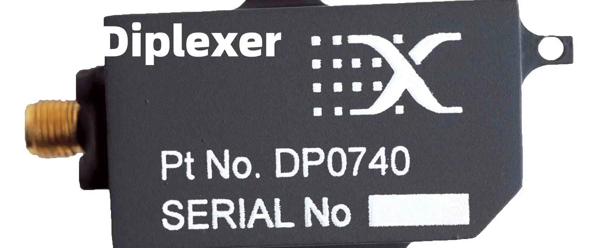
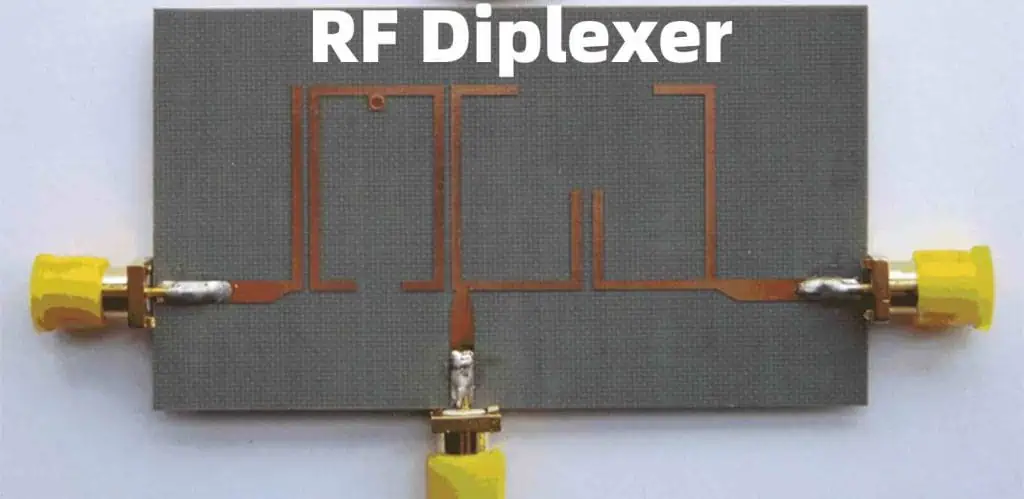
This is a three-port frequency-dependent device that combines or separates signals. A Diplexer is considered a combiner or separator of signals.  It comprises two different fixed tuned bandpass filters with a common port. The diplexer has three terminals which are formed by the output of the two filters (RX and TX).

The passband frequencies of the filter’s determine how the signals used in the common port separates. Also, the signals used in any uncommon port isolates from the uncommon port. These signals then combine at the common port. Diplexers are a type of multiplexer.

On the other hand, duplexers enable a transmitter and receiver operating on different frequencies to share an antenna with less interaction and degradation of various RF signals. A diplexer consists of an antenna port, transmitter port, and a receiver port. This device is commonly used in applications where several modulation methods and carriers function on the same antenna.

In telecommunication systems, an RF diplexer plays a crucial role. For instance, cellular base stations may have limited tower space to accommodate more antennas. Therefore, an RF diplexer can be used in this case.

When choosing a diplexer for an application, there are some things one needs to consider. The specifications of an application determine a lot. The isolation rates, the amount of signal acceptance and rejection are key factors one should consider.

What are the Features of the RF Diplexer?

Diplexer
Diplexer

An RF diplexer comes with a three-port RF filter component which is usually used in multi-band systems. Multi-band systems have an antenna that enables two frequency bands to transmit. Each of these bands can receive and transfer signals. One of the major roles of a Diplexer is to share signals according to their distinct frequencies.

The diplexer has a receiver port that get signals, a transmitter port that transfers signals and an antenna port. Also, there are two filters in a Diplexer. The transmitter port uses one of the filter’s while the other filter is used by the receiver port. The antenna port serves as a point of connection between the two filters and the antenna.

The RF diplexer isolates frequencies and carries them to the appropriate port. It as well prevents unwanted frequencies from going through the two filters. These filters can check the frequencies of signals to reject or accept them. Alternatively, a filter may be available to look for a particular frequency to enable the application to perform a certain function.

It is very possible to customize a diplexer to carry out one specific function. You can customize your diplexer to receive signals only. In this case, a lower performance diplexer is needed. Higher performance diplexers are usually needed for applications like military and aerospace. This type of diplexer will be a perfect option for use in applications that need to transmit and receive signals at the same time. To achieve this, two ports need to be available. 

What are the Design Requirements of RF Diplexers?

For the RF diplexer to offer the necessary functions without restricting the frequencies that should be received and transmitted, it is important to place standard technologies within the diplexer. These technologies include ceramic chips, wavelength diplexer topologies, lumped elements, and planar diplexer topologies. Let’s have a look at some of these technologies.

Planar diplexer

Planar diplexers are very small. These technologies offer great integrability into system components. Due to their smaller sizes, diplexers are much more ideal for more lightweight applications. Also, it is very easy to duplicate planar diplexers and the cost of this device is usually very low.

However, planar diplexer topology has its own issues. One of these issues is that it has lower power handling capabilities compared to waveguide diplexer topology.  Furthermore, planar diplexers have a lower quality factor.

Waveguide Diplexer

The waveguide diplexer is another technology. It features two different bandpass filters and a circulator. One of the benefits of these diplexers is their low insertion losses. Also, they offer high power handling capabilities which need no tuning. Furthermore, they are more selective.

A waveguide diplexer has a big size and as such can be very complex to reproduce. This can be a major concern when designing radar or telecommunication devices. Furthermore, the waveguide diplexer is more expensive. This design type may also experience integrability problems.

What is a Triplexer?

FULL PCB MANUFACTURING Quote

A triplexer is also a type of RF multiplexer. Its functions and operations differ from a Diplexer and duplexer. A 4-port filtering device that divides one major input in three various outputs with a different frequency is a triplexer. This means that a triplexer features three one output port and three input ports.

A triplexer can also be used in a reverse manner. That means it can route signals at three frequencies into one port. With a triplexer, a coaxial cable can easily get into the feed of three different antennas.

This 4-port filter device is bidirectional and it comprises 3 bandpass filters having three separate passband frequencies. You can find a triplexer in wireless transmitter and receiver systems like radar.

A multi-band wireless system with three channels for GPS, WLAN, and GSM/CDMA can make use of a triplexer. One antenna can get the signal and then route different signals to different port. In this manner, a broadband antenna can easily receive three different signals. The isolation of signal between the three ports is a crucial factor to evaluate when choosing a triplexer.

The use of passive techniques in triplexers helps to save cost and as well reduce size. A triplexer provides reduced insertion loss over each path. Also, it provides return loss at all output and input ports. A triplexer finds its use in triple-band devices for smartphones.

What is an RF Duplexer?

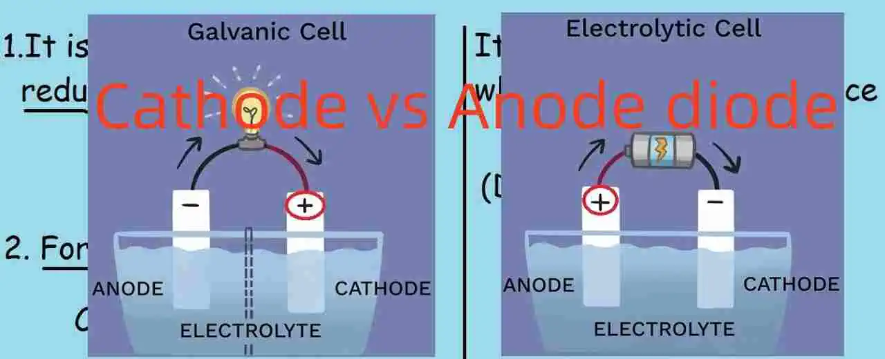
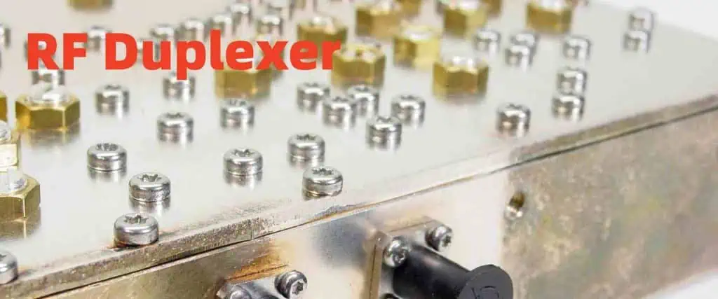
An RF duplexer is different from an RF duplexer. The duplexer uses the antenna in a communication system for transmitting and receiving signals. It is a three-port device that acts as a circulator for low-power applications. Also, an RF duplexer enables the transmission bi-directional signal over a single path.

One of the functions of duplexers is that they enable radar communications to share the same antenna while keeping the receiver away from the transmitter. RF duplexer isolates the receiver from the transmitter in order to provide two-way communication over one channel. The path between the receiver and transmitter is not a direct one. Therefore, a duplexer is often considered a circulator. This means that the signal coming from port 1 goes to port 2 while the signal coming from port 2 routes to port 3. In this case, port 1 and port 3 do not meet.

Applications of Duplexer

There are many use cases of duplexers, especially in the RF communication systems. Here are some applications of RF duplexer:

De-Multiplexing

Duplexing entails combining several RF signals in the frequency domain. This involves putting an ideal duplexer that has a high isolation filter circuitry between the antenna and Tx/Rx RF chain.

De-multiplexing occurs when you separate the combined signals into several RF signals.

Receiver protector

When RF signals are transmitting, a duplexer offers isolation between the receiver and the transmitter. Also, the duplexer prevents the reflected signal from going back to the tranitter. Engineers make use of  PIN diode limiters in front of the receiver in order  to protect the receiver.

Radio communications

Duplexers play a major role in radio communication systems. They transmit various frequency signals having close bands difference in opposite directions.

Radio Repeaters

In RF communication, a good number of radio repeaters make use of a single antenna and duplexers for the transmission and reception of RF and microwave signals.

Radar antenna multiplexing

One of the functions of duplexers is that it links an antenna to many radar systems to enable signal transmission and reception. In the long run, this helps in minimizing the space and cost required for multiple radars.

Another important use of an RF duplexer is that it offers protection to the receiver. It prevents high power transmissions from wireless transmitters that are close by.

Difference Between Diplexers and Duplexers

Most times people usually confuse the functions of these two devices. RF duplexers and diplexers are common components you will find in transceiver circuits, receiver, and transmitters for applications like radar and communication systems. Also, other sensing applications make use of RF diplexers and duplexers. Since diplexers sound similar to duplexers, people often interchange them.

Therefore, it is better to clarify the differences between these two components and how they function. The function of an RF diplexer is different from that of a duplexer. Letโ€™s look at the differences in the way these components operate.

A diplexer allows two signal paths to be used on the same transmission line. This 3-port device achieves this by using filters to divide frequency, The filters may be band-pass filters, high pass or low pass filters. With this, it is possible for the same antenna to send and receive two different frequencies. There are factors that determine how a diplexer functions. For instance, the attenuation of the filters must work well with the closeness of the signals.

An RF duplexer is also a 3-port RF device. However, its major role is to share transmitted and received signals from one antenna into two signal paths. This is usually done according to the direction of the signal. A duplexer ensures two-way communication from one antenna since these signals may operate at the same frequency.

One of the use cases of a duplexer is in the radar system. In this application, there is a need to isolate high power transmitter signals from receiver circuitry. However, an RF duplexer has some limitations in how the receive path can be isolated from the transmit path.

What is the Difference between an RF Diplexer vs Triplexer vs Duplexer?

RF Duplexer
RF Duplexer

An RF duplexer considers the signal direction to separate a receive path and a transmit path while a diplexer considers frequency with filters to separate signals. The operations of these two devices are not interchangeable. Therefore, an RF diplexer canโ€™t replace a duplexer. While duplexers are more commonly used in telecommunication systems, diplexers also play a key role in this application.

An RF triplexer is a four-port device with one output port and three input ports. This device is widely applicable in wireless communication systems. A diplexer vs triplexer vs duplexer are a type of RF multiplexer. However, they all differ in terms of their operations and applications. A Triplexer makes use of the passive techniques to reduce size. Also, this device provides ideal isolation when used between ports.

While RF triplexers have one output port and three input ports, RF diplexers have one output port and two input ports.  Also, an RF triplexer is a combinator and a separator. This device separates and combines signals of three frequency bands. In the radar system, a duplexer functions as a connection point between the receiver and transmitter and the antenna.

One of the main benefits of a duplexer is that it can use one antenna to receive and transmit signals. For instance, a duplexer is a great choice when there is one receiver and one transmitter in single channel systems. A triplexer is a better option for multi-channel systems with many receive and transmit channels.

What are the Similarities between RF Diplexer vs Triplexer vs Duplexer?

RF triplexers and diplexers are both RF components that can divide received signals at various frequencies in three or two channels. Also, these components are ideal for combining about three or two signals on the same line.

Triplexers and diplexers are commonly used in applications where there is a need to route signal at several frequencies via various paths. The main similarities between RF diplexer vs triplexer vs duplexer is that they are all RF components.

Conclusion

Diplexers, triplexers, and duplexers are all RF components. These components differ in their functions, mode of operation, and applications. However, people interchange the meaning of these components. Having compared RF diplexer vs triplexer vs duplexer, it is easy to differentiate the functions of these devices.

What are the Best PCB Montreal Manufacturing Companies?

Rogers TC600 PCB

Have you been searching for a top PCB Montreal manufacturer in Canada? Sure, Canada is known to have a very big market for different electronic appliances used today. Different companies deal with PCB assembly and manufacturing services, which promotes the global electronics industry to a different level.

Also, do you know which PCB Montreal manufacturers are active in the PCB market of Canada? Have you ever known those features you need to consider before working with a PCB manufacturer Montreal? We will find answers to all these questions and more.

Best PCB Montreal Manufacturing Companies

Isola IS680 AG PCB

Some decades before today, some Canadian companies offering PCB manufacturing were not popular names when we talk of the whole electronics world. However, this is a whole different scenario now. You must consider the Canadian PCB manufacturers when considering the best providers of pcb manufacturing and assembly services all over the world.

A1 Electronics

A1 Electronics provides different PCB assembly and manufacturing services. This PCB manufacturer Montreal Company ensures that all the demands of clients are taken care of with great sincerity. Since 2001, this PCB Montreal company has been providing customers with its PCB manufacturing services.

Furthermore, since this PCB manufacturer Montreal is ISO-certified, this company works with all the green electronics requirements. What this means is that it is responsible for ecology coupled with the maintenance of technological development.

Also, A1 Electronics makes use of modern technologies; this is how it provides full PCB manufacturing and assembly services. For their manufacturing, this PCB Montreal Company integrated cutting edge surface mo8nt technology. This is why consumers will be able to save cost and valuable time to some extent.

The capabilities of this PCB Montreal Company include:

  • Reliable Inspection
  • Customer-friendly
  • Time saving assembly

RS Electronics

RS Electronics is a PCB Montreal company that specializes in offering turnkey services to its customers located in Quebec, Montreal, and internationally for more than two decades.

There are various reasons why customers love to partner with this PCB Montreal company. First is quick-turn assembly which ensures that customers get their quotes within a day. Their turn capability is 24 to 48 hours. Also, they are well experienced in handling different turnkey projects.

Furthermore, you can be sure that this company offers high PCB quality. They have an expert team with more than 35 years professional experience. Also, this Montreal PCB manufacturer has successfully had 20 years of great and improved processes.

In addition, this Company offers high-quality PCB manufacturing.  These include low-volume PCB assembly as well as mid-volume PCB production. Also, their turnkey PCB manufacturing includes component procurement, PCB fabrication, and finally PCB assembly

Cancino Technologies

Cancino Technologies provides EMS services (electronics manufacturing services) as well as engineering services in the Montreal area of Canada.

In addition, this PCB Montreal manufacturer provides electronic design, in-house circuit board assembly, as well as circuit board layout services. Their different services cover the productโ€™s whole life cycle. This covers the schematic capture, PCB design, volume testing, production, and prototype assembly

Since 1992, this PCB manufacturer Montreal has offered manufacturing and design services to different customers all over the globe in different industries. These include rail, avionics, telecommunications, and military fields, as well biomedical.

Furthermore, Cancino Technologies offers PCBA services including ball grid array, through hole, surface mount, and more.

Bittele Electronics

With more than a decade of professional experience, this Company has been able to meet different needs of the Montreal customers that seek low volume as well as mid volume and PCB prototype assembly services.

Also, this PCB Montreal manufacturer provides the best possible support as well as work closely with the customers from assembly phase to the final delivery. Furthermore, because of their great capabilities as well as the extensive utilization of modern technologies, Bittele Electronics have been able to develop a huge customer base in the city of Montreal.

Another great feature of this Company is that they donโ€™t stress their customers with high process; instead, they provide very economical rates for medium quantity, small quantity, as well as prototype PCB assembly services.

What are the Important Attributes of a PCB Montreal Manufacturer?

FULL PCB MANUFACTURING Quote

Before considering the best ten Canada PCB manufacturers, it is very important that you consider some basic features before deciding to settle for one. Below are some important attributes.

PCB quality

Note that quality is very important when determining the best PCB Montreal manufacturer. Quality implies different things. These include getting error-free as well accurate designs that are sent into the circuit boardsโ€™ sphere. This also includes accurate board dimension, properly drilled and accurately positioned drilled holes, etc.

Ability to meet the requirements of the PCB

Top PCB manufacturers must adhere strictly to as well as work with the standard specifications of the PCB. These include the types of material (tolerance, specific requests, etc.), number of layers, as well as other major specifications.

Cost for PCB Manufacturing

The manufacturing costs of top PCB manufacturer Montreal must be reasonable. However, costs shouldnโ€™t be too low and result in low-quality products.

Collaborative Capacity

Top PCB manufacturing Companies would love to create a great relationship with their potential clients. This usually involves the partnership regarding the assembly as well as design processes. This also has to do with quick resolution of all PCB issues that arise.

Board Testing

The top PCB Montreal manufacturers must test their PCB test circuit boards before they are delivered to their customers.

RoHS Regulation

The best PCB Montreal manufacturers must implement RoHS regulations. These include the RoHS standards for restricting hazardous substances.

Conclusion

In summary, we will say that working with the best PCB Montreal manufacturers is very important. However, this may become a very stressful task. Therefore, you may decide to consider the best picks and insights that have been suggested inside this article to help reduce the process of the PCB search. In addition, you will be able to enjoy all the great benefits involved in working with the best PCB Montreal manufacturers.

Cathode vs. Anode Diode: How to Indicate Placement Orientation of Diodes on Your PCB

cathode vs anode diode

Diodes are a common part of consumer electronics. These have made our lives easier and today our most of the routine activities include diodes. These are simple components of electronics. The role of a diode is to allow the flow of current only in one path and it stops the current flowing other paths in the devices. The impedance has no influence on the current that a diode controls. There is a lot more to diodes in the field of PCB. We are going to highlight some important aspects of diodes in our discussion so letโ€™s get started without any delay!

The Diode

As you already know the current that flows through a diode cannot flow in more than one direction. Now this condition is a forward bias condition. For making it more simpler, you can consider diodes as some kind of electronic valves which regulate the current flow so that the device can keep working normally. In case a diode is experiencing a negative voltage, there will be no current flowing which will make your diode an open circuit. Besides a forward bias condition, there is also a reverse bias diode condition. Basically, biasing means that the diode is determining different amounts of voltage and current at different spots in a circuit. The diodes include semiconductors as fundamental units in their structure. The semiconductor diode has two sides called P-type and N-type. In the center, there is a P-N junction. There are also some leads connected to these diodes which make the assembling of these diodes in consumer electronics much easier.ย 

Diode Functionality

laser diode

In order to understand the diodes fully, we need to learn about their functionality. As we already know that diodes have leads and two of them connect with the sides of the diodes. The lead which joins with the N-type is called a cathode while the P-type lead is the anode. The cathode is a negative side while the anode is a positive side. Now, keep in mind that all the functioning of the diode revolves around this region in which the P-N junction is also included. We are going to take a look at the reverse and forward bias condition of a diode in detail below:

  1. Forwards Bias Condition: In case the voltage connects with the positive anode and its negative side joins with the cathode, it will make this diode a conductor and the forward bias condition will establish which means the current is flowing.
  2. Reverse Bias Condition: In this case, if we reverse the voltage sides, meaning connecting the negative side of the voltage to the anode and the positive side to the cathode, it will establish the reverse bias condition. The current does not flow in this condition. The diode becomes an insulator.

The Two Regions of a Diode

The two most important regions of a diode are its N-type and P-type regions. These regions will help you understand the working of a diode on a much deeper level. In a general diode, the cathode is always on the right side while the left side represents the anode. At the anode, the current flows from positive to negative. You can also consider a large minus sign on the cathode which shows this side of the diode is negative if you are working with a diode in a forward bias condition. 

Diode Characteristics

Itโ€™s time that we consider some salient characteristics of the diode in this section:

  • The reverse voltage of a diode means the total amount of voltage that it can allow before it undergoes complete failure and the direction of the current, in this case, is always reverse.
  • The reverse voltage of the diode also goes by peak reverse voltage or peak inverse voltage so you can learn one of the names at your convenience. 
  • There is a fixed limit of reverse voltage for every diode and increasing this limit is not recommendable at all. 
  • The maximum current rating of a diode means the total amount of peak current which flows through the diode. Just like we cannot change the reverse voltage, the peak current rating also remains constant as it causes adverse damage to the diode we are working with.
  • The diode is a versatile component for electronics means it can act as an insulator and a conductor. 
  • It has critical applications in different industries as well due to its remarkable features, efficient performance, and simplified nature. 

Anode vs. Cathode Diode

All the LEDs that you have seen or used by far contain two diodes which are cathode and anode. Without these diodes, no LED can perform efficiently. To fully learn about the LEDs, we need to understand how LED polarity works in detail. Basically, the LED polarity means the route that the current takes for following. The LEDs contain diodes and due to the presence of diodes, the current in them can only follow a single path to flow. Now, letโ€™s shed light on the anode and cathode individually in the next sections for easy understanding.  

What is an Anode?

An anode in a LED is actually a diode and is positive. An anode of LED acts as a terminal which is a door that allows current for flowing. 

What is a Cathode?

If you have understood the anode, learning about the cathode is a no-brainer. It is just contrary to the anode. Just like an anode that will allow the current to flow, a cathode in the LED will not allow it to flow and will make the current leave its route.ย 

How to Tell Anode vs. Cathode

FULL PCB MANUFACTURING Quote

Their signs will let you know! Follow the anodeโ€™s positive sign and the negative sign of the diode to differentiate between the two easily. If their signs are too small, you can use a magnifying glass for proper visualization. There are some other differences between an anode and a cathode that might be helpful for you in your upcoming diode projects. So letโ€™s get started!

The Differentiations Based on the Electrical Charge

Now you are about to learn the trick to determine the anode and cathode easily. Since these both are involved in the current flow, sometimes it becomes tricky to determine the two. The anode always captures the negative changes because it is positive. The positive charge on the anode makes it an electron receptor. Therefore oxidation takes place at the anode. The cathode is the proton receptor because it has a negative charge and attracts protons. The purpose of a cathode is to generate the electrons. Once the negative charge has been established, it will make the current follow the anode from the cathode. 

Anode vs. Cathode Diodes: The Major Differences

After this section, you will be able to easily differentiate between anode and cathode. The differences between anode and cathode include:

1. Type of Terminal

One easy way to determine the anode and cathode is that the anode is the positive terminal while the cathode is the negative terminal. 

2. Type of Charge

The anode gives away the electrons which means it undergoes oxidation while the cathode receives the charge which means reduction making it a negative terminal, unlike the anode. 

3. Electric Current Flow

The anode allows the current to enter the LED while the cathode makes the current go out of the LED. 

4. Positivity and Negativity

You can also determine the anode and cathode as per their charges. It is one of the simplest methods to determine these two terminals. The anode is always positive while the cathode is negative. 

5. Oxidation vs. Reduction

At the anode, oxidation takes place while reduction takes place at the cathode. It is also a good way to differentiate between the two. 

6. The Pinโ€™s Length

Sometimes, you can also determine both from the size of the pins which are different for both terminals. However, this is not always true since manual cutting and human errors can sometimes make them alike and it gets difficult to differentiate between anode and cathode. Donโ€™t worry, you can still determine the cathode in this regard. So it means if you get successful in finding the cathode, you can determine the anode ultimately. There are tips that will help you find the cathode in the first place:

  • If the casing if flat and joins with the diode then it is a cathode
  • If the casing is protruding a little bit then it is a cathode

Advantages of DIodes:ย 

  • Diodes ensure less short circuits
  • These are reliable for the regulation of voltage and current
  • A diode prevents overvoltage
  • Diodes dont let overcurrent damage the electronics
  • These are for easy conversion of AC to DC
  • Diodes are reliable for giving DC to electronics

Disadvantages of Diodes:

  • A semiconductor diode has its limitations for working with the extreme reverse voltage
  • Diodes are not much responsive
  • These have reverse saturation current which is not beneficial 
  • Diodes produce a higher amount of noise in some devices

Diode Orientation and Placement

Diodes are simple components. But when we talk about their polarity, they become a challenging concept. There are different types of diodes including plug-in diodes and patch diodes because their orientation and assemblies are different. The two common types of diode assemblies include DIP and SMT. Therefore it is important to determine which type of assembly you are going to use as per your diode type. If you are hiring a diode assembly firm, then you have to be careful with the diode orientation because there is no margin of negligence as it can cause diode failure. The silkscreen of PCBs is helpful so that you can have the complete diode orientation information. There are different devices that use bidirectional diodes. Proper ground planing is important to maintain their efficiency. It will also prevent the stub diodes from production and ruin the performance of consumer electronics as well. 

Donโ€™t Forget the Functional Implications of Component Orientation

There are some tips that you need to follow when you are assembling PCBs to avoid complications on all counts. It is important to consider these because the functional implications matter when we are working with PCBs. Take a look at them below: 

  • Human interface considerations: Opt for human interfacing for the PCB parts. You can rely on locked and unlocked connectors for this purpose. It is also important to position the switches and wiring so that it will improve the PCBโ€™s efficiency. Proper orientation of PCB parts is crucial so that you can easily proceed with the PCBs. Also, try to maintain a decent distance between the PCB parts so that you can avoid mishaps as much as possible and protect your PCBs from possible damage. 
  • Marking orientation: You need to make sure that your silkscreen is giving accurate statistics so that it will allow you to prevent any possible complications. The polarity indicators should be involving accurate pins for this purpose. These measures will make your marking orientation feasible. 
  • Quality validation: It is important to pay close attention to the components that are present in the form of groups or are alike in nature. If you will do this, you can greatly lower the risk of PCB reworking and assembling PCBs from scratch. Quality validation is highly crucial so that you can produce highly efficient and industrial-grade PCBs with the least hustle. 
  • Thermal performance: Thermal performance of PCB parts also matters and is different for each component. Some components are critical and sensitive and need proper orientation to allow ventilation so that they dont get damaged due to overheating. 

Summary

Diodes are highly important for the fine performance of several devices. Due to this reason, diodes need our special attention and special handling to drive positive results from them. From aerospace to defense, diodes have major applications in different domains around us. We have highlighted some major aspects of diodes in this post so that you will be able to easily understand them.

Also, you are now able to differentiate between anode and cathode easily since we have discussed some useful tips and tricks for that. We hope that diodes are now a no-brainer for you and can develop stunning diode projects in the future as well. We will catch you in the next one with something more fascinating from physics! 

Why You Should Choose a PCB Assembly Toronto Companies

CPU PCBA

Digital revolution has overtaken the world and this is reliant on PCBs. All successful applications or softwares need to function in a specific operating system which is called a device. However, take note that these gadgets are highly-dependent on a well-assembled PCB. This is why PCBs form an important part of all digital or electrical equipment.

Furthermore, cost-effectiveness and quality in printed circuit boards have become important factors that virtually all circuit board designers all over the world must take note of.

This is why getting your projects from one of the best PCB assembly Toronto companies is very important. This is because PCB Assembly is a very complex process which requires a professional and this is why you have to be very careful when choosing a PCB assembly Toronto Company.

In this article, we will be reviewing some PCB assembly Toronto companies that are well known for delivering top-notch PCB assembly.

How is Canadaโ€™s PCB Industry?

Though there has been a rise in PCB demand, production has shifted from the industrialized nations and to the developing nations, most importantly China, despite the fact that this product is widely used. For instance, in the last decade, about half of the PCB manufacturers located in North America decided to shut down their operations.

Lead times and production costs are very important when determining a Companyโ€™s commercial success. Also, there are some beliefs that the move of the industry to regions that have less-rigorous environmental restrictions, are caused as a result of very strict regulations of the government.

Moreover, the PCB assembly Toronto and then entire Canada manufacturers are increasing in number due to the demand and supply of the market. Now, letโ€™s focus on the best PCB assembly Toronto Companies.

Best PCB Assembly Toronto Companies

Candor Industries

Candor can be described as an innovative and modern PCB assembly Toronto company, ensuring their competitors are always behind them. Customers benefit so much from working with them because they create what customers dream of.

Furthermore, they deliver important innovative solutions in PCBs which permits product innovations in a whole different way. Their clients enjoy the benefits of unique processes as well as a reliable customer service that offers advances in design and technology.

Also, this PCB assembly Toronto Company is CGRP and ISO 9001:2015. This helps in the creation of new technologies and designs that require a collaboration or partnership. This process of production needs not just a reliable product, but having communication support and knowledge.

In addition, the engineering and Candor sales team are always set to assist and will offer responses to quotes and questions very quickly.

Custom Rapid Solutions

This PCB assembly Toronto Company has given computerized and simple electronic products, prototypes, as well as PCB assembly service since 2005. This Company is well-trusted for quick answers to help offer quality and quick assistance types for product prototyping within two to five days.

Also, whenever these models have been acknowledged, they provide board assembly, manufacturing in large scale, booked shipment and warehousing.

The main business and products offered by this company include PCB fabrication, PCB procurement, PCB assembly, contract manufacturing, medical devices, LED lighting, Electronic design, electronic manufacturing services, turnkey PCB assembly, automotive circuit boards and more.

RLX Solutions

RLX Solutions provide different mechanical and electronic equipment from circuit boards, manufacturing of custom cables, manufacturing of custom components, as well as custom mechanical components.

Furthermore, with the Companyโ€™s international recognition, they stand by their quick-turn and reliable solutions for production and design. RLS Solutions is a well-known authorized reseller/distributor for many LED brands and semiconductor/components.

RLX Solutions is known to offer their professional services to many OEMs residing in Toronto. Also, they carry a very strong international sales and manufacturing presence in Toronto. Since the establishment of RLX Solutions, the country has been able to grow and offer their services in more than one hundred countries. Also, you can be sure of the guarantee.

Crimp Circuits

This PCB assembly Toronto Company was established in 1980 and its base is in Toronto, Canada. Crimp circuits deal mainly woit5 the manufacturing of diverse and quality printed circuit boards. Also, it prides itself on the MFG capabilities, PCB services and products, as well as dependability when we talk of delivery of the package.

The main services offered by this PCB assembly Toronto company includes emergency circuit board services, file conversions, artwork scanning, editing, manufacturing of metal clad, metal core, flexible, and rigid printed circuit boards. They also offer quick-turn prototyping and production.

Important Considerations when Choosing the Best PCB Assembly Toronto Manufacturer

through-hole assembly process

Before you go ahead to choose a PCB assembly Toronto Company, there are some important features that you must look for. Letโ€™s consider some of them.

 Quality

Never compromise on quality. Work with PCB assembly Toronto Companies that will create high-quality products at all times. This includes the creation of error-free designs. It also contains the right size of the board, as well as holes that are adequately drilled and accurately placed.

Cost of Manufacturing

Cost should be a factor when making your choice. However, donโ€™t choose low-quality materials in a bid to reduce your overall cost. Work with PCB assembly Toronto Companies that offer high-quality PCB assembly at affordable costs.

Timescale

It plays an important role in assessing the capacity and effectiveness of a top PCB assembly Company. This assembly company must be able to deliver the printed circuit board within a particular time frame.

Materials used

Asides lowering the cost of production, top PCB assembly Toronto companies will deliver PCB materials that ensure speed, consistency, and quality in your PCB assembly and manufacturing.

Conclusion

Choosing the best PCB Assembly Toronto could be a stressful task. However it is important for anyone involved in the manufacturing or assembly of equipment or electronic devices to seek and work with professional and experienced Companies. When dealing with these PCB assembly Toronto Companies, it is best to consider each Companyโ€™s description, what their achievements are, as well as their experience to be able to choose the right one for you.

What are the Most Effective Ways to Clean PCB?

PCB Cleaning

Despite the coating with solder mask, a circuit board can still be prone to dirt and other forms of contaminants. Using the effective PCB cleaning process helps you get rid of the dirt and keep the surfaces cleaner than they were.

In this article, we reveal some of the possible reasons why your circuit board is unclean and the best possible ways to fix it.

Are Circuit Boards Unclean?

Yes, Printed Circuit Boards (PCBs) are unclean if they are kept or used in unclean environments. Certain factors could also lead to the deposition of dirt or dust on the surface.

As a consumer, you want to make sure that your boards are well-cleaned and with the right hands handling it; you donโ€™t have any problems with that.

The Types of PCB Contaminants

Both the dry and wet contaminants are responsible for the dust, dirt or debris lurking on the surface of a circuit board.

Here is a summary of how each of these contribute to the uncleanliness of PCBs:

The Wet Contaminants

As the name suggests, these are the pitfalls that necessarily have to do with water. Here are some important points worth noting about the wet contaminants of PCBs:

  • Examples of wet contaminants are soda, grime, waxy oil, water, and flux.
  • They become sources of contamination for the PCB when they are used in higher operating temperatures.
  • It is common for the wet contaminants to have difficult removal processes.
  • The best way to handle such contaminants is to get rid of them with either a vacuum or brush.
  • Leaving the contaminants for a long time tends to affect the circuit boardโ€™s performance.

How to Tackle the Wet Contaminants

The best way to clean flux from PCB is to use either a vacuum or a brush. This is the best option when you notice the contamination on time.

However, if the contaminants have been there for a while, you may consider different other approaches, such as:

Demineralized Water

This is always the best option if you want to remove moisture and contaminants from the PCB at lower operating temperatures.

Once the residual moisture is removed, make sure to properly dry the circuit board.

YouTube video

Use the IPA Cleaning Agent

Isopropyl Alcohol (IPA) is one of the PCB cleaning agents you can use too. You can dip a clean cotton cloth or a small brush into the alcohol and apply on the surface where the contaminants are.

Dry Contaminants

These are the circuit board contaminants that have to do with the likes of dirt and dust. Since they donโ€™t deal with water, one may be misled to think they donโ€™t cause much harm. On the contrary, these contaminants tend to have negative impacts on the electronic componentsโ€™ overall performances.

A few things you should know about the dry contaminants are:

  • The dust and dirt accumulate around and inside the PCB.
  • The cleaning process is usually hard, as these contaminants are more of particulates. As such, they often reach into the deepest parts of the circuit board.

How to Get Rid of Dry Contaminants in a PCB

Due to the far-reaching potentials of these contaminants, it is possible for them to get deeper into the PCB.

If you must get rid of them, quit using a brush. Instead, use a specially-designed vacuum cleaner or compressed air.

Other Possible Ways for a PCB to be Contaminated

The dry and wet methods are not the only ways your circuit board can become unclean. Other ways include:

  • The possibility of short-circuiting when a liquid with conductive properties enters the electronic components.
  • Drawing-in of debris and dust when the circuit boardโ€™s fan blows higher than expected.

The Best Cleaning Methods for Your PCB

FULL PCB MANUFACTURING Quote

Once youโ€™ve ascertained that your circuit board is in danger due to the contamination; the next step would be to get rid of them.

There are different ways to do this and we would like to start with the easiest.

1.    The Manual PCB Cleaning Process

This is often the easiest and yet, the most tactical. The manualized process takes time and works best if you are looking to get rid of wet contaminants.

You need a tiny brush and a solution, such as Acetone or Isopropyl Alcohol (IPA). To begin with, you have to:

  • Soak the circuit board in the solution (IPA or Acetone). Leave it to sit for like 10 minutes.
  • Next, use the tiny brush to work through the pathways or routes that have been contaminated.
  • Once the cleaning process is over, use a demineralized water to rinse the PCB.
  • Place it under the sun to dry for a few minutes.

Advantages of Manual PCB Cleaning

Consider the following to be some good reasons to manually remove dirt from your circuit board:

  • It doesnโ€™t require the use of specialized pieces of equipment.
  • You only need a few items โ€“ a brush and a solution, such as IPA or Acetone.
  • The cleaning solution evaporates quickly and doesnโ€™t pose much harm to human beings.

Downsides to Manual PCB Cleaning

As much as the manualized process comes in handy and can be completed in a short time, it also has some downsides.

Here are some of the reasons why it may not be a good option:

  • Using high percentages of the solution could have negative effects on the human body.
  • The cleaning process is limited to only the components and surfaces you could see.
  • As a manualized process, it takes a lot of time to complete.

2.    Cleaning a PCB with Sodium Bicarbonate (NaHCO3)

Sodium Bicarbonate, also called baking soda, can be an effective cleaning agent for your Printed Circuit Board (PCB).

It is best used for the following:

  • When getting rid of corrosion on the PCB.
  • You can also use it if you want to remove the accumulated grime on the circuitry.

Here are some of the benefits to using baking soda for PCB cleaning:

  • It helps in neutralizing the acidic properties of dirt.
  • Thanks to the mild abrasive properties, it doesnโ€™t put the PCB at risk when removing grime.

How to Clean Circuit Board Using Compressed Air

Using compressed air is a faster and unobstructive method of getting rid of dirt lurking in and around a PCB.

Here are some of the points to note:

  • Compressed air is best used if you want to clean a small amount of dirt from the circuit board.
  • Use short bursts to apply the compressed air into the circuit boardโ€™s ventilation ports.
  • You can also consider reassembling the PCB to make further applications of the compressed air. This way, you get to remove more of the dirt and dust inside the board.

3.    Clean Your PCB with Distilled Water

You can use distilled water to get rid of dirt in your PCB, but this has to be done with some moderations. Worthy of mentioning is that distilled water is a โ€œpoor conductor of ions,โ€ which is why mixing it with some cleaning solution is advised.

Here are some points to note:

  • Always protect your hands with gloves to prevent a physical contact with the solution.
  • Always seal the distilled water when itโ€™s not in use.

4.    Use PCB Ultrasonic Cleaners

Consider using ultrasonic cleaners if your Printed Circuit Board (PCB) suffers bubbles during the operation.

The use of these cleaners can help the PCB cleaning process in a number of ways, such as blasting away the contaminants on the PCB componentsโ€™ surface.

Here is a summary of how the PCB ultrasonic cleaners are designed to work:

  • The cleaners use ultrasonic sound waves of up to 20,000 Hz. These help to deploy the use of high-frequency signals to create cavitation.
  • Cavitation refers to the process of generating bubbles that are popped and leveraged to remove the additives and contaminants on the PCBโ€™s surface.

Best Practices for PCB Ultrasonic Cleaners

You can get the best results from the use of circuit board ultrasonic cleaners when you consider the following:

  • The ultrasonic cleaning process works best for the dense and complex circuit boards.
  • It is always better to use the PCB ultrasonic cleaners when cleaning boards made with the Through-Hole Technology (THT) process.

Downsides to Using PCB Ultrasonic Cleaners

It doesnโ€™t make sense to use these cleaners because of some possible disadvantages. These include:

  • The sound waves possibly cause damages to the electronic components, especially when removing dirt or grime.
  • The process is best-suited for both high-volume and dense circuit boards.

What is the Difference between Cleaning PCB and Cleaning PCBA?

There is a bit of difference between cleaning a Printed Circuit Board (PCB) and cleaning a Printed Circuit Board Assembly (PCBA).

From the surface-meaning, the former refers to the method of cleaning an ordinary circuit board, while the latter refers to the cleaning process for an assembled circuit board.

For clarity, here are the major differences between cleaning a PCB and cleaning a PCBA:

Differences in the Types of Boards

This refers to the difference in the type of circuit board. While the cleaning process of a PCB is for the basic board during the production, the PCBA cleaning process is used for the circuit board that are used with applications that have a difficult assembly process.

Differences in the Cleaning Processes

The common PCB cleaning processes are ultrasonic cleaning, the uses of distilled water, baking soda and manual cleaning. On the contrary, you are introduced to a wide range of options for the PCBA cleaning processes. These options include:

  • Aqueous Cleaning: this entails the combination of detergent and heated, deionized water to subject the PCBA to a series of rinsing cycles.
  • Vapor Degreasing: this refers to the use of an environmentally-sustainable cleaning fluid to get rid of dirt on the surfaces of miniature components.

The Basic PCB Cleaning Tools

Irrespective of the type of PCB cleaning process, the choice of tools or pieces of equipment is important. The use of these tools helps to facilitate the process of getting rid of dirt, dust and other forms of contaminants from the PCB and the components.

Here are some of the tools you need to get the job done:

1.    Isopropyl Alcohol (IPA)

You need IPA if you are using the manualized process of cleaning circuit boards.

2.    Flux Remover

This comes in handy when looking for how to clean circuit board after soldering. The function of the flux remover is to facilitate the removal of flux, after the circuit board has been soldered.

3.    Cotton Swab

Either the cotton swab or cotton clothing can be used with the Isopropyl Alcohol (IPA), Acetone or any other solution.

Dip the cotton swab or cotton cloth into the solution/solvent and use it to wipe the surface of the board where the contaminants are.

4.    Blow Dryer

Once the PCB has been cleaned, the next process is to get it dried. The drying options often include a blow dryer and an oven.

It is advised to use a blow dryer because of the excellent performance in sucking out the moisture inside the board after the cleaning process is over.

5.    Towel

You also need an alternative for drying the Printed Circuit Board (PCB). Consider getting a lint-free towel, which doesnโ€™t leave much debris behind after wiping the surface of the circuit board.

Why PCB Cleaning is Important

Cleaning the surface of a Printed Circuit Board (PCB) is important for a wide range of reasons. These reasons range from the removal of contaminants and the prevention of the same from causing negative damages to the board.

For the Printed Circuit Board Assembly (PCBA), the cleaning process does a lot of โ€œmiracles.โ€ The benefits include but are not limited to making the boards more reliable and elongating the shelf life. The benefits of cleaning a PCBA also include:

  • Boosting the chances of enhancing the PCBAโ€™s lifespan, especially after the application of the three anti-paints.
  • The PCBA cleaning process helps to bolster the reliability and high-precision required of the medical-grade and military PCBs.

Conclusion: Clean Your PCB the Right Way

The task of cleaning your circuit board appropriately lies with the manufacturer. Smart consumers work with RayPCB. We help you clean the surface of the circuits and get the dirt and other forms of contaminants away from the PCB components.

How to Test Circuit Board with Multimeter?

Test Circuit Board with Multimeter

We can never deny the importance of PCBs in our daily lives. From microwaves to washing machines, almost all consumer electronics include PCBs in their construction. Due to this reason, it is important that we understand the significance and functioning of PCBs to avoid facing complications.

If you are into PCBs, you already know that PCB inspection is highly crucial. Due to this reason, we are able to experience precision PCBs in our day-to-day house chores. There are different methods by which we can inspect a PCB. However, experts recommend relying on the multimeter.

A multimeter is a good device to inspect your PCBs to find out any defects and faults in them. We are going to have a detailed look at the usage of multimeters for the inspection of PCBs. With a multimeter, you can not only inspect the entire boards, but you can individually inspect the PCB components. Therefore are different small-to-big components in a PCB that need an in-depth inspection.

However, since the multimeter is our topic of discussion today, you should know that there are different inspecting methods that most producers use other than this. These are all reliable. However, their costs are different. Due to this reason, different producers are more likely to opt for different PCB testing methods. The common methods are:

  • AOI PCB testing free/paid
  • X-ray testing 
  • Function testing
  • Visual inspection 

It is important to know that some PCB providers also offer efficient and fully assembled PCBs along with the inspection. Therefore it depends on your situation. You can still find some producers that offer these boards at affordable prices to make them more accessible. The shipping time also varies from one producer to the other.

Sometimes they can even expedite the delivery process for you in case you are dealing with a shortage or emergency. There are also different PCB makers who specialize in different types of PCBs, from complex to simple. RayPCB is one of the best PCB professionals that you can find online. They are exceptional in their services and products. Besides, they showcase an impressive clientele due to their fine performance at the same time. Annually, several partners collaborate with RayPCB to gain from their services.

You can rely on RayPCB for their shipping service and prompt delivery. They are continuously making improvements in their services to meet the requirements of their customers. Plus, they are also introducing the latest services like CNC machining and 3D printing to attract more clients. Their solutions for technological problems and prototyping are also reliable for collaborations.ย 

What is a multimeter?

Test Circuit Board
Test Circuit Board

A multimeter is basically a PCB inspection device. The purpose of a multimeter is to detect faults in the performance of a PCB. It measures voltage, current, and resistance in PCBs to find if everything is going okay or not.

Plus, you need to carefully connect the multimeter with your PCBs to get accurate readings. A controller is present on all multimeters, which helps you get precise readings from PCBs. Today, you can rely on a digital multimeter to ensure more accuracy, and it is also easy to use. 

How to measure voltage?

Voltage means the difference between the electric potential of two points present in a PCB. These points can be anywhere in the PCB. We denote voltage with a capital V in physics. To get the accurate voltage, you need to connect it to the PCB through its terminals. These are pretty obvious, and you won’t find any problem in joining them. However, there are some rules. Join the red probe with the positive terminal, and the black one is for the negative one.

Some people mix these up, and due to this reason, they end up getting inaccurate readings. So make sure to avoid this on all counts. After joining the probes with terminals, it is time to get to the dial. Switch it to voltage mode because we want to get the voltage. Make sure that the voltage you are setting on the multimeter should be greater than the voltage of the source. A 20V is enough for measuring the voltage of a 9V source. 

How to measure continuity?

Continuity means how much electricity a circuit like PCB can conduct on average, with the help of a multimeter to measure the connectivity of a device as well. We take this in Ohms. In this case, the process is different from measuring a PCB voltage.

Now, the first thing you need to do is to detach the power source. After this, you need to connect the multimeter to the device you want to measure the continuity of. Unlike with the voltage case, you can connect the probes with any of the terminals. Switch the multimeter to the continuity mode before proceeding. It will show the precise continuity on the screen for you.

Testing a Circuit Board That is not Functional or Working

ยท       Visual Inspection

You might often have faced that the PCBs undergo failure or suddenly stop working. It can happen to other types of circuits as well. In this case, you can find out the culprit easily using some methods. The best way is to manually inspect your PCBs.

So that you can quickly identify the defects with the naked eye, there can be reasons that a PCB can stop working all of a sudden. Problems with wiring, electrical complications, or heat damage can be possible problems. Letโ€™s check out effective solutions for this problem:

ยท       Checking Power Module

The first thing you should consider is the power module. If you have manually inspected the circuit board, and there is no problem with the components, then the power module can be our culprit. Make sure to charge the power module fully. Make sure to take voltage readings through a multimeter to be hundred percent sure.

FULL PCB MANUFACTURING Quote

If the input and output values are accurate, then the circuit board is working fine. Sometimes the PCB components can undergo damage and start consuming extra current, which leads to further complications as well. Therefore checking the fuse also comes in handy. It should never. Show the value 0V because it indicates the short circuit of one or more components. Short circuits often heat up the entire board, and sensitive components get molten and completely ruined. In this case, you need to immediately separate the damaged parts and consider replacements to save your PCBs from possible failure. If overheating is not the problem, then traces can be damaged and make the PCB stop working.

ยท       Checking the Input or Output Ports

When considering the PCB culprits, the input/output ports play a huge role. Damaged I/O ports mean these will hamper the fine performance of PCBs. These ports have the potential to turn off the entire circuit in some cases.

Due to this reason, maintenance of these orts is important to save your circuits. If there is no problem with the I/O ports, then issues with the microcontroller can arise such problems. 

ยท       Checking Communication Ports

Circuit boards with communication ports can also undergo abrupt shutting down. Therefore the inspection of communication ports is important. Problems in communication can lead to heat damage and defective communication among the circuit components.

You need to make sure that the ports are working fine, or in the other case, you can ask for help. It is because there have been many cases reported that indicated problems with the communication ports led to the shutting down of circuits. 

ยท       Optimize Printed Circuit Boards for Troubleshooting

Circuit board testing is a crucial process to ensure PCBs are safe to use. Defective PCBs can not only give shocks, but they can easily catch electrical fires. Not only this, a faulty PCB can ruin the entire electronic device. Therefore, an in-depth and rigorous inspection of PCBs is not only crucial, but it ensures that the PCBs meet industrial standards.

For example, using a multimeter gives you a wide range of inspection options. You can take readings for the voltage, continuity, resistance, and current as well. Some users can do it manually. However, if you donโ€™t know the method, it is better to take professional help. Plus, you can find and hire professionals for the sake of PCB inspection. In this case, you will have more guarantees that your PCBs are just fine and will serve longer. 

Conclusion

Now you know that PCB producers cannot ignore inspecting their PCBs before delivering them to you. It is because defective PCBs not only invite more damage. But these can be unsafe to use for the users.

Due to this reason, we have discussed a multimeter for detecting PCBs. You can easily choose one inspection method and see if it fits your budget or not. In other cases, you can seek professional PCB inspection services from the providers. However, keep in mind that these services vary in terms of pricing as well.

Therefore, always consult the PCB makers for inspection services before you proceed with them. It will not only save you from loss of money and time, but it will ensure your safety too. 

STEP AP203 vs AP214 vs AP242 โ€“ What are their Basic Functions?

STEP AP203 vs AP214 vs AP242

The STEP file is a neutral 3D Computer Aided Design (CAD) file format that can exchange data among different CAD programs like Creo, Inventor, CATIA, and more.  STEP is an acronym which means Standard for the Exchange of Product Data). The popularity of the STEP file has grown among engineers and developers. This is because of its features and benefits.

This file format is an ISO standard. The EXPRESS modeling language is mainly used in writing this file. STEP is in various Application Protocols (APs). These include STEP AP203 vs AP214, vs AP242. The classification of these APs varies as regards their 3D dimensional geometry and mechanical CAD design.  We will take a look at the differences and similarities in STEP AP203 vs AP214 vs AP242 in this article. Also, we will discuss the benefits and features of each of these APs.

What is the Importance of the STEP File Format?

The STEP file format is mainly designed to enable interoperability among several CAD programs. Letโ€™s take a look at some scenarios where this file format is important. It is not easy to translate Native CAD file formats generated from CAD software to another proprietary CAD system. Therefore, the STEP file format comes in handy in this case. You only need to export the proprietary file formats into a neutral CAD format.

STEP has become popular among companies. This is because companies are now moving away from traditional paper-based workflows and are now adopting model-based definitions. These companies now make use of the STEP file format for interoperability downstream. Among several companies, the STEP 242 is the most popular file format.

STEP AP 242 contains production manufacturing information like BOM, GD&T, and notes for measuring and building assembly. With this, you can now get different workflows from one source of truth. The STEP file is compatible with many programs and as such makes collaboration quite easy.

STEP files are commonly used in architectural design and 3D modeling. This is because they offer cross-platform compatibility and a high level of accuracy. Also, STEP files can help you design well-detailed models. A good number of manufacturers use the STEP file due to the benefits it offers.

Each 3D STEP file has 3D model data which are saved in an ASCII text format. One of the amazing features of STEP file is that it can read and save the entire body of the 3D model with precision.

STEP Application Protocols

step file
step file

Each application protocol features a scope that defines its purpose. This is an activity diagram that specifies what an engineer needs to do within the scope. Also, there is an Application Requirement Model that defines the data requirements of the activities.

The most common use of STEP file format is the exchange of design data as assemblies of solid models. STEP  became a more popular choice with its 3D dimensional data exchange by setting up a forum for Cad vendors to enhance the quality of the solid model data. This success shows that enough perseverance can overcome the reluctance of vendors to adopt user-defined standards.

In 1996, it was believed that it is impossible to use neutral standards to exchange solid model geometry data between systems. STEP Tools, Inc in collaboration with Ford, Allied Signal showed how STEP was successful in exchanging data of 3D geometry. This was really a huge success.

What is STEP AP203?

AP refers to Application Protocol.  For AP203, the design of mechanical parts and configuration controlled 3d are crucial. AP 203 specifies the management data of solid models for mechanical assemblies. The defense and aerospace sectors support this file format. Also, this file format doesnโ€™t allow the management of Layers and Colors.

The second edition of AP203 is interoperable with  STEP AP214. In this edition, there is an inclusion of layers and colors. Also, there are textual annotations related to geometry in this edition. You will also find validation properties like center, volume, area, and clouds of points.

Features of STEP AP 203 include:

  • Geometrical data as faceted models, solids, wireframe, and surface models.
  • The products are mechanical assemblies and parts
  • It features data linked to documentation of security classification
  • There are data for configuration control

What is STEP AP214?

This Application protocol is for data for automotive mechanical design processes. STEP AP 214 receives support from the automotive industry. It defines every important detail in AP 203. Details such as layers, geometric dimensioning and tolerance, and plus colors of STEP 203. Also, this file format enables the management of layers and colors.

AP214 is an improved version of AP203. In 2003, STEP introduced a second edition of STEP 214. No changes were introduced in the scope but some corrections were made. STEP is already preparing the third edition of this format.

The features of this AP214 are all from AP 203. There are other features like

  • Geometric dimensioning and tolerance (GD&T)
  • Colors and layers
  • Construction history which is in 3D format
  • Validation properties which are Global and local
  • Textual annotations related to geometry
  • Kinematic structures
  • References to product data in another format other than STEP
  • Surface conditions and tolerance data

What is STEP AP 242?

STEP AP 242 has an application protocol that focuses on managed model-based 3D engineering. It makes a single standard for 3D engineering by combining STEP AP 214 and STEP AP 203. STEP AP242 includes all the features of AP 214 and AP 203. This makes it a more popular option among all the STEP file formats. It is a highly preferred STEP format for businesses.

STEP AP 242 features 3D electrical harness, 3D semantic PMI, 3D piping, 3D kinematics assembly, and 3D shape quality. Also, it has digital rights management and mechatronics.

STEP AP242 features the same shape presentation which is implemented in the CAD tool for STEP AP214. Another uncommon feature you will find in AP242 is the tessellated shape representation. This feature enables display in 3D shape by making use of a representation like triangulated faces. There is a semantic representation in STEP AP242.

What are the Differences Between STEP AP203 vs AP214 vs AP242?

FULL PCB MANUFACTURING Quote

Out of all the STEP APs explained above, the best format is the STEP AP 242. This is because it includes both the features of STEP AP 214 and STEP AP 203. Also, STEP AP 242 is an ideal format as it is a proof for MBE or MBD workflows.  The ISO/TC 184/SC 4 has withdrawn its contribution towards AP214 and AP203.

The introduction of publication of AP242 made AP 203 and AP214 to be deprecated. STEP users can track the implementation coverage of AP242 by following the work of CAx.

Furthermore, AP 203 and AP214 are very popular for model geometry. This is because the MBE or MBD workflow has just been adopted.  The difference between STEP AP203 vs AP214 vs AP242 can be seen in their features. Also, in terms of applications, STEP AP203 vs AP214 vs AP242 differ.

STEP File Viewer

The National Institute from Standards and Technology (NIST) created the STEP File Viewer. It is a free tool that enables users to open the STEP file. Also, this tool enables users to open this file to perform some functions like generation of CSV files or a spreadsheet that comprises attribute information

Also, this tool enables users to create a view of supplemental geometry, part geometry, and targets, graphical PMI annotations.  Users can as well make analysis of any graphical PMI, semantic PMI, and validation features for conforming to recommended practices.

What STEP Alternatives are Available?

Asides from STEP file formats, there are a lot of CAD-neutral file formats you can make use of. Although the STEP file offers a lot of features, other file formats are also a great alternative for developers.

JT

JT is specially designed for visual representation. However, it can consist of PMI and B-rep. This makes it MBD-ready. The majority of vendors use the JT Open Toolkit of Siemen which uses blends alongside proprietary recipes. Therefore, it is only popular within Siemen software environments.

IGES

IGES refers to the Initial Graphics Exchange Specification. This neutral file format is the oldest and it enables exchange of data among CAD systems. It enables solids and geometry. But, it has no PMI and as such, it isnโ€™t MBD-ready. IGES allows users to exchange product models in the form of wireframe and circuit diagrams.

QIF

QIF means Quality Information Framework. As a more recent ISO standard format, it has the largest scope on MBD. This is particularly for Big Data, semantic PMI for human and machine-readable CAD. QIF has some advanced concepts such as measurement and tolerancing features. This format is well used within the aerospace and defense sector, all thanks to its advanced MBE/MBD workflows.

3D PDF

This file format is very ubiquitous and easy to view on every device. You can use it for graphical representation. However, it doesnโ€™t enable automation since it has no machine-readability features. The 3D PDF features 3D geometry. Since this file is very easy to read, it makes the distribution downstream much easier.

How does STEP Help Geometric Dimensioning and Tolerancing?

In manufacturing, you need something beyond the geometric model to produce a part. Many additional specifications are needed, but a description of the tolerances is very important. This is because it will help in deciding the manufacturing process and as well as the tools needed in manufacturing the part.

When AP203โ€™s second edition was created, STEP included a model of Geometric Tolerance and Dimension (GD&T) information. GD&T was further improved in AP242. There has been several changes and CAD vendors have made feedback about functionality.

The new model of GD&T features an existing model since the GD&T data qualifies items in the geometry model. It is quite challenging to implement the GD&T model.

Applications of STEP Files

In 3D design, STEP file has become a standard. This file is commonly used in printing, architecture, and manufacturing among others. STEP file can do the following:

Share 3D models

STEP files were mainly created to make it very easy to share files that comprise 3D data. Developers use these files to print or review 3D models. STEP files have complete 3D models instead of the geometries and as such, sharing of files is very simple. Also, these files are compatible with various CAD systems.

Edit 3D models

In STEP, all three dimensional (3D) components are saved as one. You can use these components to create some design edits. The majority of CAD programs can read and edit STEP files. This enables collaboration and cross-platform design.

Frequently Asked Questions

What are the Disadvantages of STEP Files?

CAD software canโ€™t identify STEP files since they donโ€™t have the necessary texture or material data that makes them identifiable. This is not ideal for architectural design. Creating a STEP file can be time-consuming and as such, this makes it very complex.

STEP files donโ€™t store camera or lighting information. File formats like USDZ and FBX can help you represent lighting and camera setups.

How do you Open, Create, and Edit a STEP file?

You can open a STEP file by using different CAD programs. All you need to do is to locate the STEP file and right-click to select File. After that, choose Open and the file will open. If the STEP file refuses to open, there is a need to open or install the STEP file or CAD.

Creating a STEP file is as simple as editing one. When creating a STEP file, you will need to use the CAD program. After this, you can now edit your file.

Which is the best option between STEP AP203 vs AP214 vs AP242?

When it comes to STEP AP203 vs AP214 vs AP242, the best option is the AP242. This is because it has the features of both STEP AP203 and AP214.

Conclusion

STEP AP203 vs AP214 vs AP242 are common STEP file formats used in different applications. These file formats serve different functions and are used in different applications. Despite the differences in STEP AP203 vs AP214 vs AP242, these file formats share some similarities.

What is CNC Rapid Prototype Machining and How Does it Work?

CNC Rapid Prototype

CNC rapid prototype machining can be described as a great technique which permits businesses to be able to design as well as create very accurate and precise product prototypes . It deals with the utilization of computer-controlled machines to carve out product models from solid material blocks like metal or plastic. The process aids in the identification and rectification of any potential flaws or issues in the design of the product before you embark on mass production.

Furthermore, CNC rapid prototype machining is cost effective especially for small-batch manufacturing. Here, we will be explaining what rapid CNC means and give a detailed introduction, which includes its considerations, typical methods, benefits and pitfalls, applications, and more. Letโ€™s begin.

What is CNC Rapid Prototype Machining?

CNC rapid machining brings together two well-known terms in manufacturing, which are rapid prototyping and CNC machining. This deals with the creation of a prototype or physical model of a particular product from the 3D or CAD model making use of CNC machines or computer numerical control machines.

The CNC machine helps in reading instructions from the digital file and then goes ahead to translate them to accurate cutting tool movements. It results in a very accurate result as well as a consistent part which meets the right specifications.

Speaking in general terms, businesses usually work with CNC prototype machining during the fabrication of a few parts before there is a need for a larger batch. This prototype machining will serve different purposes, which includes the determination of how a specific part would look when it is completed and testing to see if it would function as it should.

Using advanced machinery and software, rapid CNC provides speed, precision, as well as customization during the process of manufacturing. If you desire a cost-effective and a quick prototype of the complex parts, then the best process available is CNC rapid prototype machining.

How Does Rapid Prototype Machining Work?

CNC Prototype
CNC Prototype

The rapid machining principle starts with the creation of the 3D designโ€™s CAD file. From this CAD file, a G-code is generated which the CNC machine will be able to interpret. Also, before rapid machining, there is a need to assess this G-code to make sure of no issues or errors. Once you are okay with the testing results, then the part is produced.

CNC rapid prototype machining is categorized as a subtractive process. Working with the G-codeโ€™s instructions, the machining of the parts is done with different electronic cutters and tools. During the stage of manufacturing, you have access to different materials. Also, after completing the rapid machining process, that part is taken out of the machine, which is then completed based on what you want.

Typical CNC Rapid Prototype Machining Methods

Rapid CNC machining deals with different methods, which involves the removal of some of the parts of a specific workpiece in order to create desired products. Letโ€™s consider these methods.

Milling

This is a method whereby this cutting tool usually rotates.ย  Whenever the milling tool comes in contact with the workpiece, the chips will be taken out. Operations related to CNC milling may cover end milling, chamfer milling, face milling, tapping, boring, drilling, etc.

Furthermore, milling is a very versatile method of fabrication with high tolerances and precision. It is great for different materials and is also fast. Its ability to create different intricate parts is a great benefit of milling. Moreover, its cons include huge waste, high cost of equipment, and requirement for different tools.

Turning

Turning signifies that a workpiece is undergoing rotation rather than that of milling where the cutting tool rotates. This tool connects to its rotating workpiece so as to help remove swarf or metal chips. In addition, CNC turning is useful for manufacturing shafts. Furthermore, you can apply it to a cylinderโ€™s interior or exterior. You can achieve turning for great accuracy.

Drilling

Drills are specifically designed to make holes, although milling machines can handle this as well. However, what differentiates both methods? Drills make use of the tip of the tool in generating a hole, whereby the milling tools work with cutting edges found around the periphery of the cutting head.

The rapid CNC drilling machines are usually utilized in automating this task, offering more economical solutions and greater precision.

Grinding

The CNC grinding machines help in the removal of materials through the spinning of the grinding wheel. Its goal is offering high-precision finishes to the metal workpiece. Also, the surface quality which you can achieve is very high. This is why, instead of measuring the last part from the raw materials, you can employ it as a finish process.

Types of Rapid CNC Machines

There are different CNC machines, which includes plasma cutters, routers, lathes, and mills. Every machine type comes with its unique capabilities and works for several applications. Furthermore, mills are utilized for drilling, cutting, as well as shaping materials like plastic or metal.

Primarily, lathes are utilized for turning the cylindrical shapes, while the routers are utilized for the cutting of intricate designs to sheet materials. The plasma cutters utilize plasma torches of high temperatures for cutting the metal through.

What are the Applications of the CNC Rapid Prototype Machining?

CNC rapid prototypes are useful in practically all industries requiring accurate machining. Furthermore, these industries usually demand some functional prototypes having features that are equal to final products. Here are some of the applications of rapid CNC machining.

Medical Industry

Medical industry equipment needs hard materials and microscopic precision. Furthermore, the industry features tight tolerance demand for several parts like implants, safe enclosures, orthotic devices, prosthetics, MRI machines, implant holders, surgical scissors, biopsy tubes, etc.

For this case, the process of CNC rapid machining can offer functional prototypes with great quality and accuracy which other methods will not be able to achieve. In addition, the medical industry enjoys a material choiceโ€™s versatility provided by prototype machining which meets the partsโ€™ requirements manufactured from plastics and metal.

Automotive Industry

CNC rapid prototype machining is great for creating prototypes of different parts in automotives. Before embarking on mass production, you have to test the prototypes to see if theyโ€™ll function effectively and suit properly inside a vehicle.

However, the automotive industry also demands parts and gears having very tight tolerances. Rapid machining creates prototypes that match the intended purpose and exact specifications.

Aerospace Industry

For aerospace, several aircraft parts can experience increased wear or drag as a result of a small error. This causes the failure of these parts when itโ€™s an airborne aircraft. Furthermore, CNC rapid prototype machining helps in testing the functionality of the part before using it in an aircraft. In addition, it offers parts having high accuracy and precision.

This industry evaluates the innovations and performance of new materials and parts constantly through the CNC rapid prototypes. Many components used in the aerospace industry, which includes bushings, landing gear ports, airfoils, manifolds, etc., are produced with the help of CNC rapid prototype machining.

Defense and Military Industry

CNC rapid prototype machining can be widely utilized in the defense and military industry. Since the majority of military and ammunition vehicles necessitates extremely intricate contraceptives in order to function effectively, prototypes are highly needed. Furthermore, the defense and military industry devices that make use of rapid machining include transportation components, plane parts, ammunition, communication components, etc.

ย Energy and Oil Industry

The energy and oil industry demands components having great strength to help in digging and extracting resources out from the extreme depths underneath the surface of the earth. Rapid CNC helps in the creation of these parts.

Construction and Architecture Industry

Construction and Architecture extensively makes use of CNC machining in fabricating the exterior and interior elements. At first, this operation was performed with the help of injection molds. This caused an increase in expenses and time. However, with cc rapid machining prototypes, it has become less expensive and faster.

What are the Benefits of CNC Rapid Prototype Machining?

FULL PCB MANUFACTURING Quote

There are many benefits that come with CNC rapid prototype machining.

Efficient and Quick

Rapid CNC is fast and very effective for creating prototypes. CNC machines with little supervision, these CNC machines can help transform 3D models into real objects within hours. This less lead time ensures faster deliveries of the finished products for the users compared to the alternative approaches of prototyping.

High Precision and Accuracy

Regarding accuracy, this methodology surpasses other methods of prototyping by a huge margin. It might be utilized in creating parts having great accuracy. There may be an increase in the surface finish through the application of sophisticated processes for finishing.

This is what makes it appropriate for fabricating the parts requiring tight tolerances for engineering and scientific applications.

Makes use of versatile materials

You may use CNC prototyping on versatile materials. As a result of technological limitations, the majority of prototyping methods like 3D printing are usually confined to specific materials. This CNC prototyping can make prototypes easily making use of the material intended for the final product.

Easily modified

There is an occasional need to make corrections to your design during the phase of product development if you discover any problems. Using a CNC rapid prototype, the task becomes an easy one. Just correcting the fist CAD design as well as reprogramming your machine will be just fine. This helps in reducing the time of the design and expedites the introduction of the product into the market.

No fixed tooling required

Majority of prototyping usually needs special tools, which have to be prepared beforehand. An example here are hardened dies that help in injection molding. This could raise the production cost as well as prolong the lead time. You don’t need any of these for CNC rapid prototype machining. This approach’s turntable has different tools. The tools may be replaced or cycled through to finish up the task.

Repeatability and Consistency

Because CNC machines are usually computer controlled, they can reproduce identical components repeatedly, with minimal deviation in quality. Also, these CNC machines help in producing successive batches with small dimensional variations. This is why they are very suitable for any manufacturing assembly requiring very tight tolerances present between the mating components.

What are the Cons of the CNC Rapid Prototype Machining

There are several reasons why the use of rapid machining is great for making prototypes. However, there are some limitations that may make the process an inappropriate one for some projects. Now, letโ€™s consider them.

It is more expensive compared to 3D printing

The creation of prototypes using CNC Machining is usually more expensive compared to other technologies such as 3D printing. As a result of running the large CNC machines as well as the extra trained labor needed, CNC prototypes are usually more expensive. However, the raw materials, which includes the metals are much more expensive than the 3D printing

Much material waste

CNC Machining can be described as a form of subtractive manufacturing. It means that the creation of the prototype is through the progressive reduction of excess material out of a block till the eventual product is revealed. This generates much waste, which affects the environment negatively and therefore increases the production cost.

Geometrical Constraints

The modern rapid CNC machines of today like 5-axis milling machines come very sophisticated that could shape or cut any complicated parts. Moreover, these machines might find some of these designs challenging.

Skilled and Technical Labor

The creation of the CAM and CAD file requires technical knowledge. In addition, setting up as well as running the CNC machine requires great skill. Expertise in the rapid CNC prototyping procedure for innovative ways, testing, experience, as well as a creative vision is necessary. In general, CNC machining operators have to be experienced and properly trained.

Conclusion

CNC rapid prototype machining is a great option when you want to produce prototypes and metal parts with better structural integrity as well as great mechanical properties. On the contrary, 3D printing is well adapted to the manufacturing prototypes so as to visualize the concepts even in little quantities.

18650 Battery vs 21700: How Do Both Batteries Differ?

18650 Battery vs 21700

SONY first introduced the lithium batteries. Li-ion is well-known in the marketplace as a result of its recyclability and high-energy density. In addition, it has been promoted greatly during the information age process of human electronics

As a result of this, lithium ion was elected as a successful technology that came to be during the twentieth century. This lithium-ionโ€™s performance with respect to fast-charging and safety can be seen in lots of electrical appliances.

There is a tough debate when it comes to comparing the 18650 Battery vs 21700. One of the popular debate questions goes thus. Why did Tesla replace the initially used 18650 battery in its electric vehicles with 21700? Also, what benefits does the 18650 battery offer? And what areas can the 21700 be applicable?

This is the article, which will help you understand and answer these questions better.

What is the 21700 Battery?

18650 Battery and 21700

The 21700 battery can be described as a short-hand for a lithium ion rechargeable battery which has its diameter as 21 mm as well as a length of about 70 mm. This battery first became well-known during their utilization in different electric cars like electric scooters and Tesla. Presently, it is usually utilized in flashlights and vaping.

Benefits of 21700 Battery Cells

In the Tesla Model 3, the batteries used were changed from the initial 18650 to the 21700 cells. This has caused so many people to wonder what makes 21700 batteries so special. Below are some important benefits you should know.

Greater cell capacity

There is a limitation in the 18650 cellsโ€™ battery capacity which is limited to about 3600mAh due to its size. Moreover, the 21700 battery can reach its highest capacity at 5000mAh, which is a 42 percent increase.

Also, for the e-cigarette or flashlight users, this means that about 142% of the initial running time for the single charges. This is invaluable especially for the heavy users. Since, they are not up to 1โ€ in diameter, the flashlights that use these batteries could still fit into the standard 1โ€ weapon holsters and mounts!

Low cost for every Wh

Regarding the official information of Tesla, the cost of the 21700 battery system is around $155 per kWh. The 18650 battery on the other hand costs $171 per kWh. There if the 21700 cells were installed on the Tesla Model 3, then the battery system cost will be reduced by around 9%.

In fact, our calculation reveals that the 18650 battery needs extra raw materials so as to attain a similar capacity battery pack. This is why it comes with a higher cost.

Explaining further, a battery capacity of about 100Ah could be made up of 20 units of 200mah of the 21700 cells. However, when making use of the 18650 battery, it has to use up about 30 units of 3300mah of the 18650 cells.

Higher Energy Density

Working with the official disclosures of Tesla, the 18650 battery vs 21700 battery energy densities are about 250wh/kg and 300wh/kg respectively. Working with this comparison, the 21700 batteryโ€™s energy density is almost 20% more than the energy density of the 18650 battery.

What are the Applications of the 21700 Cells?

Car

Tesla uses the Panasonic 21700 cell of 5000mAh for their car Tesla model 3

Flashlight

Fenix can be described as a company that manufactures lighting products. One of their flashlights (PD36R) specially makes use of the 21700 battery cells. This company clarified that after changing from the 18650 to the 21700 cells, there was a great improvement in the duration time for each battery

Vaping

Electronic cigarettes arenโ€™t sensitive with respect to cost. The fact is that some people wish to buy the vaping which can be utilized for a long time at 142%.

What is the 18650 Battery?

FULL PCB MANUFACTURING Quote

The 18650 battery can be described as a lithium ion rechargeable battery which has a diameter of 18 mm as well as a length of 65 mm. As a result of their superior discharge rate and capacity, they are usually utilized in scooters, laptops, flashlights, as well as devices that consumer high power.

Furthermore, Tesla Model S makes use of the 18650 cells. This cell first became well-known in some electric cars such as electric scooters and Tesla.

Benefits of the 18650 Battery

Since the original design of the 18650 battery, it is still very useful and relevant today. Many scooters, tricycles, as well as other consumer products still make use of the 18650 cells. Below are the main benefits of the 18650 battery.

 Effective Heat Dissipation Performance

When comparing the 18650 battery vs 21700 battery, you will discover that the thickness and winding length of the 21700 battery is larger than the 18650 battery. Also, regarding heat dissipation, when both batteries work, the 18650 battery comes with a better performance.

Adequate supply and high-cost performance

Over three decades ago, Sony launched the 18650 battery. In 2017, Panasonic and Tesla jointly launched the 21700 battery. The expansion of the market for the 18650 battery vs 21700 battery has been on for two decades and five years respectively. So itโ€™s clear that the 18650 cells have a greater market expansion. Furthermore, in markets, there are over 50 manufacturers involved in the production of the 186500 cells, in contrast to the less than 10 manufacturers involved in the production of the 21700 cells.

Also, this leads to the idea that 18650 batteries present on the marketplace have always been at affordable prices and insufficient supply.

How to Produce the 18650 Cells?

The manufacturing processes of the 18650 battery vs 21700 battery are virtually the same. Just the โ€œwindingโ€ pattern comes with a little difference. Furthermore, the 21700 battery is fatter and usually requires extra turns in contrast to the 18650 battery that is slimmer and requires less turns.

What are the Types of 18650 Batteries?

You can fund different types of 18650 batteries in the market. They come with different capacities, ranging between 2Ah and 3.5Ah. Furthermore, the different types have different cycles because they have different production processes and different cycle lives. The NCM 18650 cells come with a lifespan of about 300 to 1000 times.

What are the Applications of the 18650 Battery?

The 18650 battery is applicable in the following.

18650 Battery vs 21700 Battery: Are they the Same?

So many people have been confused about the difference between the 18650 battery vs 21700 battery. They are not the same, but different. First, the 18650 battery is a lithium cylindrical battery which has a diameter of 18 mm as well as a height of 65 mm. However, the shape of the 21700 cell is cylindrical, while its diameter and height are slightly larger at 21 mm and 70 mm respectively.

Another difference between 18650 battery vs 21700 battery is their capacity. The capacity of the former falls within 2600mAh and 3600mAh, while that of 21700 battery is between 4000mAh and 6000mAh. What this means is that the 21700 battery lasts longer compared to the 18650 battery before recharging.

Although both batteries can be utilized in small and portable devices, certainly they arenโ€™t alike. However, both of them share one purpose. This is to power all our gadgets. At times, you may discover that these batteries have close voltage measurements, there are extra digits close to the end, which reveals the number of amp hours every cell offers before exhaustion.

Majority people believe that the 18650 battery vs 21700 battery are identical for most parts when we talk of their performance. The major difference is that the 21700 battery seems to be much more prominent when it comes to size. Therefore, if you seek for a battery which offers the best possible performance, then any of the two between 18650 battery vs 21700 battery will be perfect.

It is very important to known that 21700 batteries would be a bit too big to fit into the 18650 battery holder.

18650 Battery vs 21700 Battery: Which is Better?

The capacity of a battery is measured in milliamp hours (mAh) or amp hours (Ah). The 21700 battery comes with a capacity of around 4000 mAh and 6000mAh, while the 18650 battery capacity falls between 2600mAh and 3600mAh. This means that the capacity of the 21700 battery is about two times that of 18650 batteries.

Furthermore, the main disadvantage of making use of the 21700 battery is because they arenโ€™t as standard compared to the 18650 batteries. This is why finding them may be more difficult and they could be more expensive. Moreover, with the great increase in the popularity of the 21700 batteries, this will most probably change very soon.

With respect to the market analysis conducted recently, the most popular of all the 21700 batteries is the Samsung lithium-ion INR21700-40T. This battery capacity is high at 4000mAh and it has maximum outputs of 40A. This makes it great for any high-drain device. Also, it features the latest charging technology of Samsung. This allows fast charging of about 15 minutes when utilized with any compatible chargers.

In addition, they are lots of 18650 batteries present in the marketplace. However, users believe that the best is Panasonic lithium-ion NCR18650B battery. High quality batteries provide great performance as well as long life. Furthermore, it is priced reasonably compared to other well-known brands.

Does the 21700 Battery Fit the 18650 Battery?

It is very important to take note that 21700 batteries would be a bit too big to fit into the 18650 battery holder. Moreover, speaking generally, the 21700 batteries would fit into the 18650 battery holder. This may not be great for performance reasons.

Also, there are concerns regarding if the 21700 battery will or will not overheat when placed in the 18650 holders. There is nothing to worry about as both batteries have different sizes and shapes. Therefore, they wonโ€™t make any contact, neither will any short circuits.

18650 battery vs 21700 battery: What are the Similarities Between them?

The similarities found between 18650 battery vs 21700 batteries are striking. These types of batteries are useful in different devices that require a source of power like smoke alarms or flashlights, etc. Also, they have high capacity in contrast to other options. Examples here are alkaline battery, and the Nickel metal hydride battery.

Both of them have a cylindrical shape and with respect to length, they have slight differences. This additional length ensures additional capacity. The battery capacities between 18650 battery vs 21700 battery are 3600mAh and 6000mAh respectively. Also, both batteries are majorly lithium-ion batteries.

Another similarity between 18650 battery vs 21700 battery is that they are rechargeable and could be utilized in devices, which need a power between 3.2 and 3.7v depending on if it is lithium iron or lithium ternary phosphate power.

Related Questions

Can the 21700 battery be used in vapes?

The 21700 battery can be used in vapes. However, ensure the battery works well with whatever vape mod you are using. Also, not all the mods will work perfectly well with all the batteries.

Can I make use of the 21700 battery instead of the 18650 battery?

Yes you can. However, take note that not all the 21700 batteries out there are created equally. Some are specially designed for different low-drain applications and some for high-drain applications.

Final Thoughts: 18650 battery vs 21700 battery

Today, 21700 batteries are now more popular. The 21700 battery provides extra power compared to the 18650. This makes it great for any high drain device like power tools and electric cars. Though several manufacturers still release some compatible products, many individuals still believe that the 21700 batteries would eventually take the place of the 18650 battery as the only industry standard.

Also, if you are seeing a long-lasting and powerful battery to help with you project, make sure that you consider making use of the 21700 battery. Asides explaining the differences between 18650 battery vs 21700 battery, we also compared the differences, as well as the differences between the lithium, batteries and other battery types such as ni-mh vs li-ion battery, with the belief that find something valuable and get some useful and reliable information.

PCB Middle Tg vs High Tg PCB: How Do They Differ?

TG150 PCB

Changes in temperature could have a significant effect on the quality, reliability, and operation of PCBAs. Increase in temperature leads to the expansion of the materials, however, the main materials which a printed circuit board is composed of feature disparate coefficients of thermal expansion.

This leads to mechanical stress, which may create undetected micro-cracks during the electrical tests (short/open tests) which is performed when the manufacturing is coming to a close. The best case scenario is that the micro-cracks would result in failures that are detected once brazing is completed. While the worst case scenario is that this could lead to different failures of your finished product.

In 2002, when the RoHS directives were introduced, it required the utilization of lead free alloys for the purpose of soldering. The removal of lead leads to an increase in melting temperature; therefore PCBs are subject to greater temperatures during the soldering process (wave and reflow). Regarding the reflow process chosen (double, single, etc.), it is very important to make use of a printed circuit board having the appropriate mechanical characteristics, most especially one having a suitable temperature for glass transition.

What is Temperature of Glass Transition (Tg)?

The Multi-layers High Glass Transition (TG) Printed Circuit Boards Manufacturer

Tg can be described as a mechanical property which designates the temperature of glass transition. This is the temperature whereby the base material (glass or polymer) decides to shift from its rigid, solid, and glassy state to a new rubbery state. Whenever the Tg has been exceeded, then materials will not melt, but will have to pass through structural changes in order to be rubbery.

Measuring this temperature precisely is very difficult to achieve since so many factors usually come into play. These include the molecular structure of the material. This is why different materials usually come with their own temperatures for glass transition. However, it is possible for two materials to share one pcb Tg value even though their technical characteristics are different. The viscosity of a material increases whenever it is heated. Also, after cooling, they easily undergo breaking or cracking.

What Does PCB Tg Mean?

PCB Tg temperature of a polymer system can be described as the temperature whereby a material changes from its relatively glassy and stiff state to one that is softened or pliable. This thermodynamic change in material can be reversed so far the polymer system isnโ€™t degraded. Explaining further, whenever that material gets a heat that is higher than the Tg and then made to cool to the Tg, it will return to the stiffer state and with its initial properties.

Most base materials usually have organic contents in them. At least, the PCB base hydrocarbons, binders, have lower stability of temperature compared to the inorganic constituents of the composite materials.

Chemists spent so many great efforts in improving the polymersโ€™ thermal properties, making them good as binders. Moreover, these properties remained at a distance from the thermal stabilities of metal foil, reinforcing glass fibers, and ceramic fillers.

Furthermore, they are great to use in different lead-free technologies, initially, a slight increase in the soldering temperature, in fact, resulted in being significantly higher compared to the stability of temperature of the PCB bindersโ€™ polymers.

What are the Major Properties of the PCB Tg Material?

A dielectric PCB substratesโ€™ main property is its thermal expansion when in a transverse direction. This means across reinforcing layers. This holds especially true for the HDI boards that are distinguished by the utilization of the thin plated holes present in the thick board base.

Furthermore, the difference in the thermal expansion of the metal and base in the holes can result in a great decrease in the interconnectorsโ€™ reliability. Moreover, if this material is heated to any temperature that is much greater than the glass transition temperature, then there may be irreversible changes in the properties. This temperature whereby this happens varies with the material type is relevant to the polymerโ€™s degradation

What are the Classes of the PCB Tg?

FULL PCB MANUFACTURING Quote

High Tg PCB

All the time, we stress that higher Tg value PCB are usually better. However, this isnโ€™t usually the case. Although it holds true that higher Tg value PCB would lead to delaying the start of great thermal expansion for any specific polymer system, the expansion as a whole might still be different for each material. Materials having lower glass transition temperature might exhibit lower net expansion compared to materials having higher glass transition temperature.

PCB high Tg results when there is a rise in temperature to a specific range leading to a transition of the substrate from its initial glassy and rigid state to a state that is more rubbery. The temperature at which this happens is referred to as the temperature for glass transition or glass transition temperature of the circuit board.

We can explain further by saying it is the highest possible temperature in โ„ƒ, whereby the substrate will maintain its rigidity. This means that ordinary materials of the PCB substrate usually exhibits melting, deformation, softening, as well as a sharp drop in the electrical and mechanical properties, when under very high temperatures.

In general, the materialโ€™s Tg is higher than 130โ„ƒ whereas the high Tg FR4 usually stands at a PCB Tg value greater than 170โ„ƒ. Medium Tg usually stands higher than FR4 Tg150 PCB. Tg170 PCB materials having a Tg of at least 170โ„ƒ are called high Tg FR4 PCBs.

An increase in the substrateโ€™s Tg helps in enhancing the moisture resistance, heat resistance, chemical resistance, as well as the stability of the PCB. Furthermore, higher values of Tg indicates that the material is exhibiting a greater temperature resistance, most especially in the lead-free processes whereby there is a prevalence of PCB high Tg applications.

Main Features of the High Tg PCB

  • Great resistance to any thermal stress
  • Dimensional stability
  • The mechanical performance is improved
  • High plated through hole reliability
  • High resistance to heat

What are the Applications of the High Tg PCBs?

Communication Equipment

Most times, high Tg FR4 PCB is used in communication equipment like network equipment, fiber optic devices for communication, and wireless base stations. Usually, these devices require great electrical reliability and performance in high-frequency and high-temperature environments.

Industrial Control Equipment

Most times, high Tg PCBs are utilized in robotics, automation systems, and industrial control equipment. Typically, these devices operate in high humidity, high temperature, as well as high vibration environments that require great mechanical strength and thermal stability.

Automotive Electronics

High Tg PCBs are utilized in sensors, on-board computers, dashboards, as well as other critical systems. A carโ€™s interior usually experiences significant fluctuations in temperature, so the materials of the circuit board that can withstand high thermal stress and temperatures are required.

Aerospace

This industry demands a high temperature resistance and high reliability from electronic devices. The high FR 4 Tg PCBs are used extensively in satellites, aircraft, as well as navigation equipment for withstanding extreme changes in temperature as well as harsh conditions for working.

Medical Devices

There is a need for medical equipment to function under high-temperature disinfection and sterilization conditions. High Tg PCBs are useful in missile control, radar systems, tactical equipment, military communications, as well as other fields.

What Benefits does High Tg PCB Offer?

High temperature durability

Usually, high Tg PCBs have great resistance to very high temperatures as well as maintain a great performance regardless of extreme thermal stress. They don’t deform or warp as a result of heat and they stay sound structurally.

Great Mechanical Strength

The high Tg PCBs are known to be very resilient and have the ability to withstand high stress and pressure. Inherently, they are strong and hard, and with each additional layer, there is an increase in their durability.

Better reliability

High Tg PCBs are much more dependable compared to the conventional PCBs. Also, they can perform optimally even in harsh and extreme temperatures. This ensures constant electrical performance even during extremely harsh conditions.

Great Power Density

Normal PCBs can’t work with high power densities due to the components that generate much heat. Moreover, the high Tg PCBs have the ability to tolerate conditions of high temperature. This allows them to dissipate heat very effectively. With these, you can place more components on the board and not be worried about overheating.

What are the Properties of high Tg PCBs?

With the quick development of our electronics industry, the PCB high Tg materials are widely utilized in communication equipment, computers, precise instruments as well as apparatus and so on.

Towards high functionality, the high multilayer development, the PCB substrate material requires higher resistance to heat as a prerequisite. Also, the boards are more inseparable from the substrateโ€™s high heat resistance, in case thereโ€™s small aperture, thinning, and fine wiring due to the emergence as well as development of a high density mounting technology, which is represented by CMT and SMT.

Therefore the difference between high FR4 Tg and the general FR-4 is the adhesion, mechanical strength, water absorption, thermal decomposition, dimensional stability in hot states, most especially after the absorption of water, which are the differences in several conditions like thermal expansion, and it is clear that the high Tg PCB is much better compared to the normal PCB substrate materials. Therefore thereโ€™s a huge demand on the high Tg PCBs recently, i.e. Tg150 FR4 despite that the price is higher compared to the ordinary ones.

In addition, the High Tg material is well-known in the LED lighting industry. This is due to the fact that LEDโ€™s heat dissipation is higher compared to the usual electronic components. However, this same FR-4 board structure is less expensive than the metal core PCBs.

The following are the properties of high Tg materials:

  • Its thermal expansion is low
  • Resists high temperatures
  • Great mechanical properties
  • Its PTH reliability is excellent
  • It has a high thermal stress resistance value

When Do I Need High Tg PCBs?

tg130 pcb

If your PCB will not be able to bear a thermal load that is not more than 25โ„ƒ less than the Tg, then you have to get a high Tg PCB to work with your applications. Also, if your own product is running at a range of 130โ„ƒ or more, then you will need the high Tg PCBs to ensure safety.

The major reason for using the hightg PCBs is due to the movement into the RoHS PCB. Therefore, there are other PCB industries that are leaning towards the use of high Tg materials.

What is PCB Middle Tg Material?

Substrates usually vary in terms of their material composition, insulating properties, and flame resistance. There are common raw materials such as glass cloth, bakelite, and other plastic boards.

The process of manufacturing a copper foil board involves pressing the copper foil with an insulating prepreg. This prepreg comprises epoxy resin and glass cloth. The base material for a rigid substrate is a non-flexible insulator. Rigid substrates have hard base material.

The base material of flexible substrates is made of flexible insulators. Most PCBs are made of rigid substrates. You can classify rigid substrate based on the materials used for them and their resin content. The base material can comprise paper and glass cloth while epoxy and phenol are best used as the resin.

What are the Applications of a Middle Tg PCB?

Middle Tg PCBs have proved to be very useful in many applications. Single sided substrates are commonly used for paper phenolic substrates. Also, this PCB is suitable for consumer electronics. You will find them in phones, keyboards, radio cassette players, game consoles, and stereos.

Middle Tg PCB are applicable in silver through-hole substrates in which copper plating can’t form through-holes. However, through-holes can be formed by filling the holes with silver paste.

What Thermal Analysis Techniques are available for PCB Middle Tg?

A crucial aspect electronic manufacturers usually consider when using circuit boards is thermal performance. A PCB will perform well if the material used in fabricating it has great thermal reliability. This makes it very important to always evaluate the thermal performance of a circuit board material.

When it comes to the PCB Middle Tg, there are several techniques for thermal analysis.

Thermomechanical analysis

It evaluates the extent of the changes in a materialโ€™s physical properties in response to varying temperature. The thermomechanical analysis (TMA) measures the changes in the physical appearance of PCB Middle Tg in response to temperature changes. TMA can also evaluate some properties like volume, density, and physical dimensions of a material.

It determines the changes in these properties in response to force and temperature. Furthermore, TMA can measure the dimensional changes of Middle Tg PCB. The glass transition of a material can be evaluated through this analysis.

Thermogravimetric analysis

Thermogravimetric analysis measures the impact of temperature on PCB Middle Tg materialโ€™s weight. TGA is a common analysis technique used in determining the relationship between weight loss and temperature. The engineer carrying out this analysis weighs the material at room temperature first. Then the analysis checks how the material changes when exposed to a particular amount of heat. This is usually carried out in a controlled environment.

Dynamic mechanical analysis

DMA helps to determine the Viscoelasticity of PCB Middle Tg. Viscoelasticity is the combination of viscosity and elasticity. This analysis also determines this materialsโ€™ resistance to deformation when exposed to vibration. DMA evaluates the extent at which a PCB material stretches and bends when it is in motion. You can use this analysis to evaluate Tg since temperature changes can impact a materialโ€™s thermal property.

Benefits of Middle Tg PCB Material

PCB Middle Tg material has many features which contribute to the performance of a circuit board.

Anti-CAF property

The PCB middle Tg material is resistant to Conductive Anodic Filament (CAF). This makes it suitable for the fabrication of circuit boards. PCB manufacturers are concerned about CAF during fabrication. CAF always occurs between adjacent PCB vias.

Environmentally friendly

One of the amazing benefits of PCB Middle Tg material is that it contains no phosphorus and halogen. This makes it safe for the environment.

UL-94 flammability

This PCB material is UL-94 V-0. It adheres to the PCB flammability standards. The UL-94 flammability is a popular standard in the PCB industry. It classifies how PCB materials burn in different scenarios.

Excellent thermal performance

PCB Middle Tg material features great thermal properties which contribute to its thermal performance. For instance, this material has low Z-axis CTE and middle Tg. Materials with middle glass transition temperature are known to perform exceptionally well. These PCB materials are ideal for fabricating rigid circuit boards and other high-performance boards.

Conclusion

High Tg in PCB i.e. PCB tg150, fr 4 high Tg, Tg 180 pcb results when there is a rise in temperature to a specific range leading to a transition of the substrate from its initial glassy and rigid state to a state that is more rubbery. The temperature at which this happens is referred to as the temperature for glass transition or glass transition temperature of the circuit board. Middle Tg of PCBs has proved to be very useful in many applications. Single sided substrates are commonly used for paper phenolic substrates. Also, this PCB is suitable for consumer electronics.