IPC-2610 represents a comprehensive suite of standards developed by the IPC (Association Connecting Electronics Industries) to address the evolving documentation requirements for electronic equipment in an era transitioning from traditional paper-based processes to intelligent digital data transfer. This standard series emerged from the recognition that conventional documentation methods, while functional, were becoming inadequate for the increasingly complex and fast-paced electronics manufacturing environment.
Powered By EmbedPress
Historical Context and Evolution
The electronics industry’s documentation journey began with Gerber files, which served the industry adequately when designs were simpler and layer counts were lower. However, as Computer Aided Design (CAD) and Computer Aided Manufacturing (CAM) tools advanced, and as trace sizes decreased while layer counts increased, the limitations of Gerber files became apparent. The industry recognized the need for more sophisticated data transfer solutions that could handle the growing complexity while maintaining accuracy and reducing errors.
IPC initially developed the GenCAM Initiative through various Data Transfer Solutions (DTS) programs from 1997 onwards, while simultaneously, Valor was developing the ODB+ format. This led to what the industry press termed the “Data Format Wars,” with various stakeholders waiting to see which format would prevail. The resolution came through industry cooperation, culminating in the release of IPC-2581 in February 2004, which incorporated the best features of both competing formats.
The IPC-2610 Framework
IPC-2610 was approved in 2004 to establish requirements for documenting electronic equipment and methodologies for revision control and configuration management. The standard applies to both hard copy and electronic data descriptions, recognizing that the transition to intelligent data transfer doesn’t eliminate the need for human-readable documentation but rather transforms how that documentation is created, managed, and utilized.
The IPC-2610 series consists of several sectional standards, each addressing specific aspects of electronic product documentation:
IPC-2611: Generic Requirements for Electronic Product Documentation
IPC-2612: Sectional Requirements for Electronic Diagramming Documentation (Schematic and Logic Descriptions)
IPC-2613: Sectional Requirements for Assembly Documentation (Electronic Printed Board and Module Assembly Descriptions)
IPC-2614: Sectional Requirements for Board Fabrication Documentation (Printed Circuit Board Description Including Embedded Passives)
IPC-2615: Sectional Requirements for Dimensions and Tolerances
IPC-2616: Sectional Requirements for Electrical and Mechanical Part Descriptions
IPC-2617: Sectional Requirements for Discrete Wiring Documentation
IPC-2618: Sectional Requirements for Bill of Material Documentation
Classification System and Grades
IPC-2610 introduces a sophisticated classification system with three grades that define the balance between hard copy documents and electronic data:
Grade A documentation consists primarily of hard copy documents and dimensionally stable film. This represents the traditional approach with 60-90% hard copy documentation and only 10-40% electronic data.
Grade B documentation represents a hybrid approach, mixing electronic data with hard copy materials. The electronic documentation may include both intelligent and non-intelligent files such as PDF views. This grade typically contains 30-80% electronic documentation, 10-60% hard copy, and 10-60% data files.
Grade C documentation consists entirely of intelligent electronic data, representing the most advanced approach with 60-100% data files and minimal to no hard copy documentation. The information is typically provided in industry-standard electronic formats or supplier derivatives.
Each grade also incorporates completeness criteria numbered 1, 2, and 3, which correspond to design, fabrication, assembly, and test requirements. The combination of grade letter and completeness number creates a comprehensive classification system that clearly defines the scope and format of documentation packages.
JISSO Hierarchy and System Integration
A significant contribution of IPC-2610 is its incorporation of the JISSO (Interface and Solution Technology) concept, which originated in Japan. This hierarchical framework describes six levels of electronic system integration:
Level 0 (Intellectual Property): Ideas and intelligence described in formal documents, design entities, or patent disclosures
Level 1 (Electronic Element): Bare die or discrete components ready for mounting
Level 2 (Electronic Package): Containers that protect elements and provide connection terminals
Level 3 (Electronic Module): Sub-assemblies with functional blocks containing elements and packages
Level 4 (Electronic Unit): Groups of functional blocks designed for specific system purposes
Level 5 (Electronic System): Complete, market-ready units combining and interconnecting functional blocks
This hierarchy provides a structured approach to understanding how documentation requirements scale with system complexity and helps define appropriate documentation strategies for different levels of integration.
Documentation Package Components
Traditional documentation packages have consistently included fabrication drawings, assembly drawings, bills of materials, schematic or logic diagrams, wiring diagrams, specification control drawings, electronic data, and mechanical drawings. IPC-2610 recognizes that while the transition to intelligent data transfer changes how these documents are created and managed, the fundamental need for comprehensive documentation remains unchanged.
The standard emphasizes that humans still need to understand what is being transferred and to whom, regardless of how sophisticated the data transfer mechanisms become. This human element ensures that documentation serves not only automated manufacturing processes but also design review, quality control, field service, and maintenance activities.
Revision Control and Configuration Management
One of the critical aspects addressed by IPC-2610 is the management of revision control for electronic data files. Traditional methods for handling revisions of paper documents needed adaptation for digital formats. The standard establishes principles for data file revision control that parallel those used for hard copy or electronic document release systems, incorporating structured formats with release data elements and attributes that define release conditions.
Industry Impact and Future Direction
IPC-2610 represents a fundamental shift in how the electronics industry approaches documentation, moving from static, format-driven processes to dynamic, data-centric methodologies. The standard encourages companies to migrate from traditional documentation to intelligent data formats, requesting CAD suppliers to support automated data export in standard formats wherever possible.
The preferred implementation approach involves providing data in convergence formats like IPC-2581, though the standard acknowledges that other documented formats remain useful provided recipients can process the files effectively. This flexibility ensures that the transition to intelligent data transfer can occur gradually while maintaining compatibility with existing systems and processes.
IPC-2610 ultimately serves as a bridge between traditional documentation practices and the future of intelligent manufacturing, providing the framework necessary for industry-wide adoption of more sophisticated, accurate, and efficient documentation methodologies that support the complex requirements of modern electronics manufacturing.
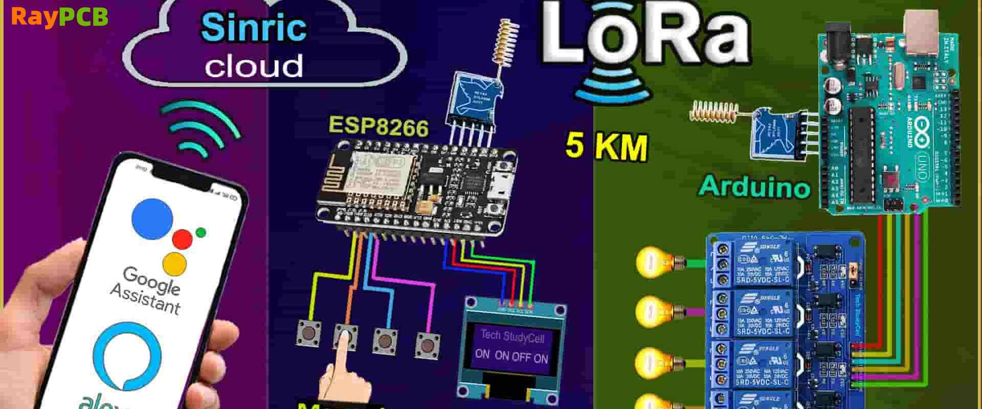
In the rapidly evolving world of IoT and home automation, the ESP32 microcontroller stands out as a powerful and versatile platform for creating sophisticated control systems. This comprehensive guide will walk you through building an 8-relay control system that combines the convenience of wireless connectivity with the reliability of physical controls. Whether you’re automating your home lighting, controlling industrial equipment, or managing irrigation systems, this project provides a robust foundation for your automation needs.
The ESP32’s dual-core processor, built-in WiFi and Bluetooth capabilities, and extensive GPIO pins make it ideal for this application. By the end of this project, you’ll have created a system that can be controlled through web interfaces, mobile applications, and traditional physical switches, offering maximum flexibility and redundancy.
Components and Materials
To build this system, you’ll need the following components:
The relay module should be chosen based on your load requirements. Most 8-channel modules can handle 10A at 250V AC or 10A at 30V DC per channel, making them suitable for most household and light industrial applications.
Hardware Setup and Wiring
The hardware setup forms the backbone of your control system. Proper wiring is crucial for both functionality and safety.
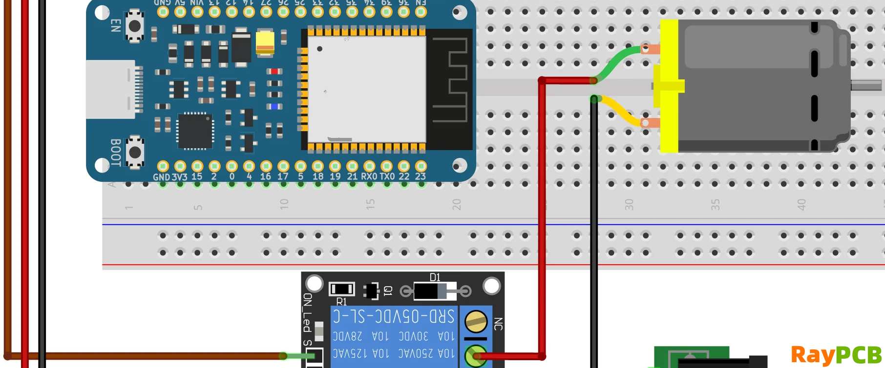
ESP32 to Relay Module Connections: Connect the control pins from the ESP32 to the relay module’s input pins. Typically, you’ll use GPIO pins 2, 4, 5, 12, 13, 14, 27, and 33 for the eight relays. Ensure the relay module’s VCC is connected to an appropriate power source (usually 5V) and ground is common between the ESP32 and relay module.
Physical Switch Integration: Each physical switch should be wired with a pull-up configuration. Connect one side of each switch to ground and the other side to a GPIO pin (such as pins 15, 16, 17, 18, 19, 21, 22, and 23). The internal pull-up resistors of the ESP32 can be used, eliminating the need for external resistors in many cases.
Power Considerations: The ESP32 operates at 3.3V logic levels, while most relay modules require 5V signals. Fortunately, most ESP32 GPIO pins are 5V tolerant on their inputs, and the 3.3V output is usually sufficient to trigger 5V relay modules. However, if you encounter issues, consider using level shifters or transistor buffers.
ESP32 Programming Fundamentals
Programming the ESP32 for this application involves several key components: WiFi connectivity, Bluetooth communication, web server functionality, and GPIO management.
Library Requirements: Your code will need several libraries including WiFi.h for network connectivity, BluetoothSerial.h for Bluetooth communication, WebServer.h for creating a web interface, and EEPROM.h for storing relay states persistently.
Basic Structure: The program should initialize all GPIO pins, establish WiFi connection, start the Bluetooth serial service, and create a web server. The main loop should continuously monitor physical switches, handle web requests, and process Bluetooth commands while maintaining relay states.
Relay Control Functions: Create functions to control individual relays and groups of relays. Implement state persistence so the system remembers relay positions after power cycles. Consider adding timing functions for automatic shutoff or scheduled operations.
WiFi Control Implementation
WiFi connectivity transforms your relay system into a networked device accessible from anywhere on your local network or, with proper configuration, from the internet.
Network Configuration: Implement both station mode for connecting to existing networks and access point mode for direct connections. Store WiFi credentials in EEPROM to survive power cycles. Include a configuration mode that allows users to set up WiFi without hardcoding credentials.
Web Interface Development: Create a responsive web interface that displays the current state of all relays and provides controls for individual and group operations. The interface should work well on both desktop and mobile devices. Use HTML5, CSS3, and JavaScript to create an intuitive user experience.
REST API Implementation: Develop a RESTful API that allows external applications to interact with your relay system. Include endpoints for getting relay states, setting individual relays, controlling relay groups, and retrieving system status. Implement proper HTTP response codes and JSON formatting for easy integration with home automation platforms like Home Assistant or OpenHAB.
Security Considerations: While not always necessary for local networks, consider implementing basic authentication for your web interface. Use HTTPS if sensitive controls are involved, and implement rate limiting to prevent abuse.
Bluetooth Control Implementation
Bluetooth connectivity provides an alternative control method that doesn’t require network infrastructure, making it perfect for portable applications or backup control.
Serial Communication Protocol: Design a simple command protocol for Bluetooth communication. Commands might include “R1:ON” to turn on relay 1, “R1:OFF” to turn it off, “STATUS” to get all relay states, and “RESET” to turn off all relays. Keep commands short and intuitive for easy manual testing.
Mobile App Integration: While you can use any Bluetooth terminal app for basic control, consider developing a custom mobile application for the best user experience. The app should provide a clear interface showing relay states and allowing easy control of individual relays or predefined groups.
Command Processing: Implement robust command parsing that handles various input formats gracefully. Include error checking and appropriate responses for invalid commands. Consider adding commands for configuration changes, such as setting relay names or default states.
Physical Switch Integration
Physical switches provide the most reliable control method and serve as an essential backup when wireless methods fail.
Debouncing Implementation: Implement software debouncing for your physical switches to prevent false triggers from mechanical contact bounce. A simple delay-based approach or more sophisticated state machine can be used depending on your application’s responsiveness requirements.
Switch Modes: Consider implementing different switch modes such as toggle (each press changes the state), momentary (relay is on only while switch is pressed), and latching (switch position directly controls relay state). Allow configuration of switch behavior through the web interface or Bluetooth commands.
Priority Systems: Decide how to handle conflicts between control methods. For example, should a physical switch override wireless commands, or should the last command take precedence? Implement clear priority rules and communicate them to users through documentation and interface design.
Safety and Reliability Considerations
When working with relay systems that control real-world devices, safety must be a top priority.
Electrical Safety: Always follow proper electrical safety practices. Use appropriate wire gauges for your current loads, include fuses or circuit breakers in your circuits, and ensure proper grounding. Never exceed the relay’s rated capacity, and consider derating for continuous loads.
Firmware Reliability: Implement watchdog timers to recover from system freezes. Include fail-safe modes that turn off all relays if the system encounters critical errors. Store critical system states in non-volatile memory to maintain consistency across power cycles.
Error Handling: Build comprehensive error handling into your code. Monitor WiFi connection status and attempt reconnection if the connection is lost. Include diagnostic functions that can report system health through all available interfaces.
Troubleshooting Common Issues
Several common issues may arise during construction and operation of your relay system.
Connectivity Problems: If WiFi connection fails, check credentials and signal strength. Implement a fallback access point mode for reconfiguration. For Bluetooth issues, verify pairing procedures and check for interference from other devices.
Relay Control Issues: If relays don’t respond correctly, verify power supply voltage and current capacity. Check all connections, particularly ground connections between the ESP32 and relay module. Ensure GPIO pin assignments match your code configuration.
Switch Response Problems: If physical switches are unreliable, review your debouncing implementation and consider adjusting timing parameters. Check for proper pull-up configurations and verify switch mechanical integrity.
Applications and Use Cases
This versatile relay system can be adapted for numerous applications across different domains.
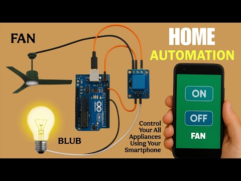
Home Automation: Control lighting circuits, ceiling fans, garage doors, irrigation systems, and pool equipment. The multiple control methods ensure accessibility whether you’re at home or away, with physical switches providing reliable local control.
Industrial Applications: Manage conveyor systems, pump controls, heating elements, and motor starters. The robust design and multiple control interfaces make it suitable for industrial environments where reliability is crucial.
Agricultural Systems: Automate greenhouse ventilation, irrigation systems, feeding mechanisms, and lighting controls. The WiFi connectivity allows remote monitoring and control of agricultural operations.
Advanced Features and Extensions
Consider implementing additional features to enhance your system’s capabilities.
Scheduling and Automation: Add time-based control functions that can turn relays on or off at specific times or intervals. Implement sunrise/sunset calculations for lighting control or astronomical timers for various applications.
Sensor Integration: Connect sensors to unused GPIO pins to create responsive automation. Temperature sensors, motion detectors, light sensors, and moisture sensors can trigger relay operations automatically.
Data Logging: Implement logging of relay state changes with timestamps. Store logs locally or transmit them to cloud services for analysis and monitoring of system usage patterns.
Conclusion
Building an ESP32 8-relay control system with WiFi, Bluetooth, and physical switch control creates a powerful and flexible automation platform. The combination of wireless convenience and physical reliability makes this system suitable for a wide range of applications, from home automation to industrial control.
The ESP32’s capabilities, combined with careful hardware design and robust software implementation, result in a system that is both powerful and reliable. By following the guidelines in this article, you’ll create a control system that can grow with your needs and adapt to various applications.
Remember that the key to a successful relay control system lies in careful planning, proper implementation of safety measures, and thorough testing. Start with simple applications and gradually expand functionality as you gain experience with the platform. The flexibility of the ESP32 platform ensures that your system can evolve and improve over time, making it a valuable long-term investment in your automation projects.
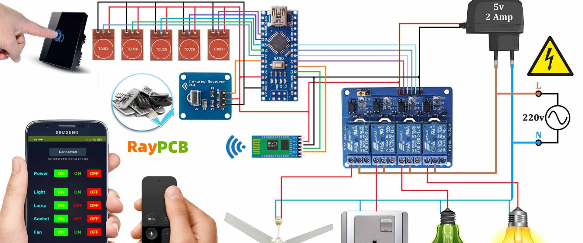
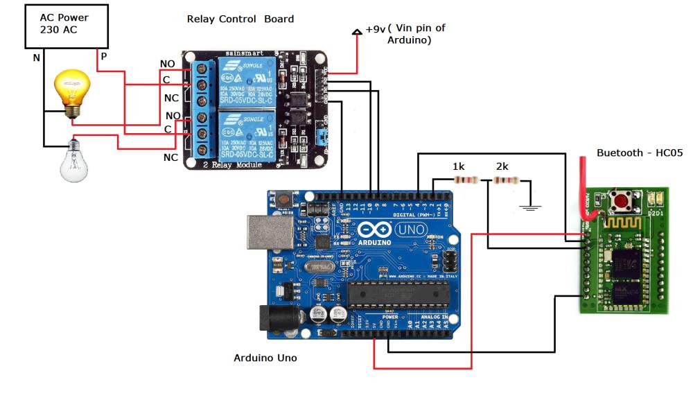
Bluetooth Low Energy (BLE) has revolutionized the way we think about smart home automation. Unlike traditional Bluetooth, BLE consumes significantly less power while maintaining reliable communication, making it perfect for battery-powered smart home devices. When combined with Arduino’s accessibility and versatility, BLE opens up endless possibilities for creating custom smart home solutions that are both cost-effective and tailored to your specific needs.
This comprehensive guide will walk you through building a complete BLE-based smart home system using Arduino, covering everything from basic sensor nodes to a centralized control hub. By the end, you’ll have the knowledge to create your own network of interconnected smart devices that can monitor your home environment, control appliances, and respond to your commands through a smartphone app.
Understanding BLE Architecture for Smart Homes
BLE operates on a client-server model where devices can act as either peripherals (servers) that advertise services, or centrals (clients) that scan and connect to these services. In a smart home context, your Arduino-based sensors and actuators typically function as peripherals, while a central hub or smartphone app acts as the central device.
The key advantages of BLE for smart homes include ultra-low power consumption (devices can run for months or years on a single battery), fast connection establishment, and the ability to create mesh-like networks through multiple connections. Unlike Wi-Fi based systems, BLE devices don’t require internet connectivity to function, making your smart home more resilient and privacy-focused.
Essential Hardware Components
To build your BLE smart home system, you’ll need several key components. The heart of each device will be an Arduino-compatible microcontroller with built-in BLE capability. The ESP32 is an excellent choice, offering both Wi-Fi and Bluetooth functionality in a compact, affordable package. Alternatively, you can use Arduino boards with separate BLE modules like the HM-10 or Nordic nRF52832.
For sensors, consider including temperature and humidity sensors (DHT22 or SHT30), motion detectors (PIR sensors), light sensors (photoresistors or TSL2561), and door/window sensors (magnetic reed switches). For actuators, you’ll want relays for controlling high-voltage devices, servo motors for physical controls, LED strips for lighting, and buzzers for alerts.
Additional components include breadboards and jumper wires for prototyping, resistors and capacitors for circuit protection, 3D printed or purchased enclosures for finished devices, and batteries with voltage regulators for portable devices. A central hub device, which could be another ESP32 or a Raspberry Pi with BLE capability, will coordinate communication between devices.
Setting Up the Development Environment
Begin by installing the Arduino IDE and adding support for your chosen microcontroller. For ESP32 boards, add the ESP32 board package through the Board Manager. Install essential libraries including the BLE library for your platform (ESP32 BLE Arduino for ESP32 devices), sensor libraries for your specific components (like DHT sensor library for temperature sensors), and JSON libraries for structured data communication.
Create a project structure that separates concerns: maintain separate files for BLE communication functions, sensor reading functions, actuator control functions, and configuration settings. This modular approach makes your code more maintainable and reusable across different devices.
Implementing Basic BLE Communication
Start with a simple BLE server that advertises a custom service. Your Arduino device should create a BLE server, define custom services and characteristics for your data (like temperature readings or switch states), advertise the service so other devices can discover it, and handle read/write requests from connected clients.
Here’s the basic flow: initialize BLE and create a server, define a service UUID and characteristic UUIDs, set up callbacks for connection events and data requests, start advertising with a recognizable device name, and continuously update characteristic values with fresh sensor data.
For the client side (which might be another Arduino acting as a hub), implement scanning for devices, filtering devices by service UUID, connecting to discovered devices, reading characteristic values, and maintaining connections or reconnecting when needed.
Building Smart Sensor Nodes
Temperature and humidity monitoring nodes are perfect starting projects. These devices read environmental data periodically, update BLE characteristics with new values, enter deep sleep mode between readings to conserve battery, and wake up on timer interrupts or external triggers.
Motion detection nodes add security functionality to your system. They monitor PIR sensor state changes, immediately notify connected clients when motion is detected, include timestamp information with alerts, and can trigger other devices through the central hub.
Light monitoring nodes help with automated lighting control. They measure ambient light levels, provide data for automatic lighting decisions, detect day/night cycles, and can trigger morning/evening routines.
Door and window sensors enhance home security by monitoring entry points. They detect state changes using magnetic reed switches, send immediate notifications on state changes, maintain low power consumption through interrupt-driven operation, and can integrate with alarm systems.
Creating Actuator Control Devices
Smart switches form the backbone of home automation. These devices receive commands via BLE to control connected appliances, provide status feedback to confirm state changes, implement safety features like auto-shutoff timers, and can operate both manually and remotely.
Smart lighting controllers offer customizable illumination. They control LED strips or smart bulbs through PWM or digital signals, support color and brightness adjustment commands, implement smooth transitions between lighting states, and can follow scheduled lighting patterns.
Servo-controlled devices enable physical automation. They receive position commands via BLE, control window blinds, door locks, or valve positions, provide position feedback for verification, and include limit switches for safety.
Developing a Central Control Hub
The central hub coordinates all BLE devices in your smart home network. It scans for and connects to multiple BLE peripherals simultaneously, maintains a device registry with current states and capabilities, implements automation rules and device interactions, provides a unified interface for external control, and logs device data for analysis and troubleshooting.
The hub should handle device discovery by periodically scanning for new devices, automatically connecting to known devices, updating device registries with current information, and managing connection failures gracefully. For automation logic, implement rule-based triggers (like “when motion detected, turn on lights”), scheduled events (like “turn off all lights at midnight”), and inter-device communication coordination.
Mobile App Integration
While not strictly Arduino code, consider how your BLE smart home system will interface with smartphones. Most mobile platforms support BLE communication through native APIs. Your mobile app should scan for and connect to your central hub or individual devices, provide intuitive controls for device management, display real-time sensor data and device states, allow configuration of automation rules, and send push notifications for important events.
Design your BLE services with mobile integration in mind. Use standard UUIDs where possible, implement clear data formats (JSON is often ideal), provide device information characteristics, and support both polling and notification-based updates.
Security and Privacy Considerations
BLE security is crucial for smart home systems. Implement device authentication using custom pairing procedures, encrypt sensitive data transmissions, use non-obvious service and characteristic UUIDs, implement access control for critical functions, and regularly update device firmware for security patches.
Consider implementing a simple authentication system where devices must provide a shared secret before accessing control functions. This prevents unauthorized devices from controlling your smart home systems.
Power Management and Optimization
Efficient power management is essential for battery-powered BLE devices. Implement deep sleep modes between operations, wake up only for scheduled tasks or external interrupts, use efficient sensors and components, implement adaptive sampling rates based on activity, and monitor battery levels with low-power warnings.
Optimize BLE communication by minimizing connection time, using efficient data formats, implementing local decision-making when possible, and batching multiple updates when appropriate.
Troubleshooting and Testing
Common issues include connection failures, power management problems, sensor reading errors, and timing issues. Implement comprehensive logging, provide diagnostic modes for testing, use serial output for debugging, and create test routines for individual components.
Build test harnesses for individual components before integrating them into the full system. This modular testing approach helps isolate problems and verify functionality.
Expanding Your System
Once your basic BLE smart home system is operational, consider adding advanced features like mesh networking for extended range, integration with existing smart home platforms, voice control through connected assistants, remote internet access through gateway devices, and machine learning for predictive automation.
Document your implementations thoroughly and consider sharing successful designs with the maker community. The Arduino and smart home communities benefit greatly from shared knowledge and open-source solutions.
Conclusion
Building a BLE-based smart home system with Arduino offers an excellent balance of functionality, cost-effectiveness, and customization potential. The low power consumption of BLE makes it ideal for battery-powered sensors, while Arduino’s ecosystem provides easy access to a vast array of components and libraries.
Start with simple sensor and actuator nodes, build up to a central control hub, and gradually add automation logic and mobile integration. Remember that smart home systems evolve over time, so design your architecture with expansion and modification in mind.
The key to success is starting small, testing thoroughly, and building incrementally. With patience and persistence, you’ll create a smart home system that’s perfectly tailored to your needs and preferences, while gaining valuable experience in IoT development and home automation.
Whether you’re looking to monitor your home environment, automate routine tasks, or simply explore the possibilities of connected devices, a BLE-based Arduino smart home system provides an excellent foundation for innovation and experimentation.
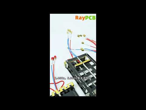
The proliferation of unmanned aerial vehicles (UAVs) in civilian and commercial applications has created unprecedented security challenges across critical infrastructure, public venues, and restricted airspace. As drone technology becomes more accessible and sophisticated, the need for effective counter-drone defense systems has grown exponentially. Radio frequency (RF) based counter-drone systems represent one of the most versatile and widely deployed solutions, with antenna design serving as a critical component that determines system performance, coverage, and operational effectiveness.
Counter-drone RF systems operate through multiple mechanisms including detection, classification, tracking, and neutralization of unauthorized drones. The antenna subsystem plays a pivotal role in each of these functions, requiring specialized designs that can handle diverse frequency bands, provide adequate gain and directivity, and maintain robust performance in challenging electromagnetic environments. This article examines the technical aspects of RF antenna design and production specifically tailored for counter-drone defense applications.
RF Counter-Drone System Fundamentals
Counter-drone RF systems typically operate across multiple frequency bands to address the various communication and control channels used by modern drones. The primary frequency bands of interest include:
ISM Bands: The 2.4 GHz and 5.8 GHz Industrial, Scientific, and Medical (ISM) bands are extensively used for drone control links, first-person view (FPV) video transmission, and telemetry data. These bands require antennas with moderate to high gain characteristics and the ability to handle both narrowband and wideband signals.
GPS/GNSS Bands: Global positioning system frequencies around 1.2-1.6 GHz are critical for drone navigation. Counter-drone antennas targeting these bands must provide sufficient gain and pattern coverage to effectively disrupt navigation signals while maintaining precision in spatial selectivity.
Cellular Bands: Modern drones increasingly utilize cellular communication (700 MHz to 2.6 GHz range) for beyond-visual-line-of-sight (BVLOS) operations. Antennas for these applications must accommodate multiple cellular standards and frequency allocations across different regions.
Proprietary Frequencies: Some drone manufacturers use proprietary communication protocols operating in various frequency bands, requiring broadband antenna solutions or multiple specialized antenna elements.
The operational modes of counter-drone RF systems directly influence antenna design requirements. Detection and monitoring systems require antennas with wide beamwidth patterns and high sensitivity to identify drone signals across large coverage areas. Active jamming systems need high-power handling capabilities and focused beam patterns to maximize effective radiated power toward target drones while minimizing interference to other systems.
Antenna Design Considerations for Counter-Drone Applications
Frequency Coverage and Bandwidth
Counter-drone antennas must provide adequate performance across wide frequency ranges to address the diverse communication technologies employed by different drone platforms. Broadband antenna designs are often preferred to simplify system architecture and reduce component count, but this approach requires careful optimization to maintain consistent gain and pattern characteristics across the entire operational bandwidth.
Multi-band antenna designs offer an alternative approach, providing optimized performance at specific frequency bands while potentially reducing overall system complexity. These designs typically employ multiple radiating elements or frequency-selective structures to achieve the desired multi-band characteristics.
The bandwidth requirements also depend on the specific counter-drone technique employed. Narrowband jamming systems may require antennas with more modest bandwidth characteristics but higher efficiency and power handling capability. Wideband noise jamming systems demand antennas with extremely wide bandwidth to ensure effective signal disruption across all potential drone communication channels.
Radiation Pattern and Coverage
The radiation pattern requirements for counter-drone antennas vary significantly based on the intended application and deployment scenario. Airport perimeter protection systems may require omnidirectional coverage to detect approaching drones from any direction, while point defense systems for critical facilities might employ highly directional antennas to focus energy on specific threat sectors.
Sector antennas with 60° to 120° azimuth beamwidth are commonly used to provide coverage of specific areas while allowing multiple antennas to create comprehensive protection zones. These antennas typically feature moderate gain levels (8-15 dBi) and controlled sidelobe levels to minimize interference with adjacent systems.
High-gain directional antennas (20-30 dBi) are employed for long-range detection and jamming applications, particularly in scenarios where the threat approach vectors are predictable or limited. These antennas may incorporate beam steering capabilities through electronic or mechanical means to track moving targets and maintain optimal signal engagement.
Specialized radiation patterns may be required for certain applications, such as null-fill antennas that provide coverage directly overhead to detect small drones operating at low altitudes, or antennas with shaped beams to conform to specific geographic constraints or regulatory requirements.
Power Handling and Efficiency
Counter-drone jamming systems often require significant RF power levels to ensure effective signal disruption at operationally relevant ranges. Antenna power handling capabilities must exceed the maximum transmitted power with adequate safety margins to prevent component failure or performance degradation under continuous operation.
The power handling requirements extend beyond simple average power considerations to include peak power handling for pulsed or burst transmission modes, as well as thermal management under sustained high-power operation. Antenna design must incorporate appropriate materials and construction techniques to handle the thermal stresses associated with high-power RF transmission.
Antenna efficiency directly impacts the overall system power requirements and thermal management complexity. High-efficiency antenna designs reduce the power consumption and heat dissipation requirements for the overall counter-drone system, enabling more compact and cost-effective implementations.
Environmental and Mechanical Requirements
Counter-drone systems are typically deployed in demanding outdoor environments, requiring antennas that can withstand extreme temperatures, precipitation, wind loading, and potential exposure to corrosive environments. Radome designs must provide adequate weather protection while minimizing impact on antenna performance across the operational frequency range.
The mechanical design must accommodate the dynamic requirements of scanning or tracking systems, including precise positioning accuracy, rapid movement capabilities, and long-term reliability under repeated motion cycles. For fixed installations, the mechanical design must provide stable antenna orientation under wind loading while maintaining precise electrical performance characteristics.
Size and weight constraints often limit antenna design options, particularly for mobile or rapidly deployable counter-drone systems. Antenna designs must balance performance requirements against practical constraints imposed by vehicle integration, transportation limitations, and setup time requirements.
Antenna Types and Configurations
Phased Array Systems
Phased array antennas have emerged as a preferred solution for advanced counter-drone applications due to their electronic beam steering capabilities, rapid scanning speeds, and ability to simultaneously engage multiple targets. These systems employ arrays of radiating elements with variable phase relationships to create steerable beam patterns without mechanical movement.
Active electronically scanned arrays (AESA) incorporate dedicated transmit/receive modules for each antenna element, providing the highest performance and flexibility but at increased cost and complexity. Passive electronically scanned arrays (PESA) use a centralized transmitter with phase shifters to control beam direction, offering reduced complexity while maintaining electronic scanning capabilities.
The design of phased array systems for counter-drone applications must address several unique challenges including wide-angle scanning requirements, multi-band operation, and integration of both detection and jamming functions within the same aperture. Element spacing, array geometry, and beamforming algorithms must be optimized for the specific operational requirements and frequency bands of interest.
Log-Periodic and Spiral Antennas
Broadband antenna designs such as log-periodic dipole arrays (LPDA) and spiral antennas are well-suited for counter-drone applications requiring wide frequency coverage. Log-periodic antennas provide consistent gain and radiation patterns across wide frequency ranges, making them ideal for detection systems that must monitor multiple drone communication bands simultaneously.
Spiral antennas offer circular polarization characteristics that can be advantageous for counter-drone applications, as many drone communication systems employ circular polarization to improve link reliability. The inherently broadband nature of spiral antennas simplifies system design while providing adequate gain for many counter-drone scenarios.
Design optimization for these broadband antenna types focuses on achieving the desired frequency coverage while maintaining consistent performance parameters. Balun design, feed network optimization, and structural considerations all impact the final antenna performance across the operational bandwidth.
Horn and Reflector Antennas
High-gain applications such as long-range detection and focused jamming often employ horn antennas or reflector-based designs. Horn antennas provide excellent control over radiation patterns and can handle high power levels while maintaining good efficiency characteristics. Pyramidal horns are commonly used for linearly polarized applications, while circular horns may be preferred for circular polarization requirements.
Reflector antennas, including parabolic dishes and shaped reflector designs, can provide very high gain levels for applications requiring maximum effective radiated power or sensitivity. These antennas may incorporate dual-band feeds to operate across multiple frequency ranges or multiple feeds to create multiple simultaneous beams.
The mechanical design of horn and reflector antennas for counter-drone applications must address pointing accuracy requirements, environmental protection, and integration with tracking or scanning mechanisms. Radome design becomes particularly critical for these antenna types due to their size and the need to maintain precise electrical performance.
Microstrip and Printed Circuit Antennas
For applications requiring low-profile, lightweight, or conformal antenna solutions, microstrip patch antennas and printed circuit antenna arrays offer attractive design options. These antennas can be fabricated using standard printed circuit board manufacturing techniques, enabling cost-effective production and easy integration with electronic systems.
Patch antenna arrays can provide moderate gain levels with controlled radiation patterns suitable for many counter-drone applications. The planar nature of these antennas makes them ideal for integration into vehicle-mounted systems or architectural installations where visual impact must be minimized.
Design challenges for microstrip antennas in counter-drone applications include achieving adequate bandwidth for multi-band operation, handling power requirements for jamming applications, and maintaining performance consistency across production quantities.
Production and Manufacturing Considerations
Materials and Manufacturing Processes
The selection of materials for counter-drone antenna production must balance electrical performance, environmental durability, cost considerations, and manufacturing feasibility. Conductor materials typically include copper, aluminum, or specialized alloys chosen for their conductivity, corrosion resistance, and mechanical properties.
Dielectric materials play a critical role in antenna performance, particularly for microstrip and printed circuit antenna designs. Low-loss dielectric materials with stable electrical properties across temperature and frequency ranges are essential for maintaining consistent antenna performance. For high-power applications, thermal conductivity and power handling capabilities become additional selection criteria.
Manufacturing processes must be capable of maintaining tight dimensional tolerances to ensure consistent electrical performance across production quantities. For RF applications, dimensional variations on the order of small fractions of a wavelength can significantly impact antenna performance, requiring precision machining, controlled assembly processes, and comprehensive quality control measures.
Quality Control and Testing
Production testing of counter-drone antennas requires comprehensive verification of electrical performance parameters including gain, radiation patterns, input impedance, and efficiency across the operational frequency range. Automated test equipment and anechoic chamber measurements are typically required to verify antenna performance to specification limits.
Environmental testing must verify antenna performance under the expected operating conditions including temperature extremes, humidity, vibration, and mechanical stress. Accelerated life testing may be employed to verify long-term reliability under operational stress conditions.
For high-power jamming applications, power handling verification requires specialized test equipment and procedures to safely verify antenna performance under maximum power conditions. Thermal imaging and temperature monitoring during high-power testing can identify potential failure modes or performance degradation mechanisms.
Cost Optimization and Scalability
Production cost optimization for counter-drone antennas involves balancing performance requirements against manufacturing complexity and material costs. Design for manufacturability principles should be applied early in the development process to identify cost-effective production approaches while maintaining required performance levels.
Scalable manufacturing processes become important considerations for large-volume production, particularly for applications such as airport security systems that may require numerous antenna installations. Automated assembly techniques, standardized interfaces, and modular design approaches can reduce production costs and improve manufacturing consistency.
Supply chain considerations for specialized RF materials and components require careful planning to ensure production continuity and cost stability. Alternative material specifications and qualified supplier networks can provide flexibility in production planning and cost management.
Performance Optimization and Integration
System-Level Considerations
The integration of antennas into complete counter-drone systems requires careful attention to electromagnetic compatibility, mechanical interfaces, and thermal management. Antenna placement and orientation must be optimized to minimize mutual coupling between multiple antennas while maximizing coverage effectiveness.
Feed network design and transmission line routing significantly impact overall system performance, particularly for multi-antenna configurations. Low-loss transmission lines, proper impedance matching, and minimal insertion loss are critical for maintaining system sensitivity and efficiency.
Calibration and alignment procedures must be established to ensure consistent performance across multiple antenna installations and to maintain performance over the operational lifetime of the system. Reference antenna standards and measurement procedures enable verification of performance specifications in field installations.
Advanced Technologies and Future Trends
Emerging technologies such as metamaterial antennas and reconfigurable antenna systems offer potential advantages for future counter-drone applications. Metamaterial structures can enable antenna designs with enhanced directivity, reduced size, or novel beam shaping capabilities that may improve counter-drone system effectiveness.
Software-defined antenna systems with electronically reconfigurable characteristics can adapt to changing threat scenarios and operational requirements without hardware modifications. These systems may incorporate machine learning algorithms to optimize antenna performance based on observed drone behavior and environmental conditions.
Integration with artificial intelligence and autonomous systems represents a growing trend in counter-drone technology, requiring antennas that can support high-speed data communications and real-time coordination between distributed sensor and jamming systems.
Regulatory and Operational Considerations
Counter-drone antenna systems must comply with relevant regulatory requirements regarding RF emissions, frequency allocations, and power limitations. Different regions may have varying regulatory frameworks that impact antenna design requirements and operational constraints.
Coordination with existing RF systems such as air traffic control radar, cellular networks, and satellite communications requires careful frequency planning and antenna design to minimize interference potential. Antenna radiation pattern control and frequency selectivity become critical factors in ensuring compatible operation with other RF systems.
Operational safety considerations include RF exposure limits for personnel, protection of sensitive electronic systems from high-power RF fields, and failsafe mechanisms to prevent unintended RF emissions. Antenna design must incorporate appropriate safety interlocks and monitoring systems to ensure safe operation in populated areas.
Conclusion
The design and production of RF antennas for counter-drone defense systems represents a complex engineering challenge that requires integration of advanced RF design techniques, robust manufacturing processes, and comprehensive system-level optimization. As drone technology continues to evolve and proliferate, counter-drone antenna systems must adapt to address new threats while maintaining compatibility with existing RF infrastructure and regulatory requirements.
Future developments in antenna technology, including metamaterials, artificial intelligence integration, and advanced manufacturing techniques, will continue to enhance the effectiveness and capabilities of counter-drone defense systems. The critical role of antenna design in determining overall system performance ensures that continued innovation in this field will remain essential for maintaining effective protection against unauthorized drone activities.
Success in counter-drone antenna development requires close collaboration between RF engineers, system integrators, and end users to ensure that antenna designs meet the practical requirements of operational deployment while providing the performance characteristics necessary for effective drone defeat capabilities. As the threat landscape continues to evolve, antenna technology will remain at the forefront of counter-drone system advancement.
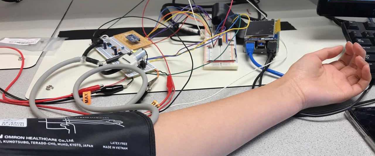
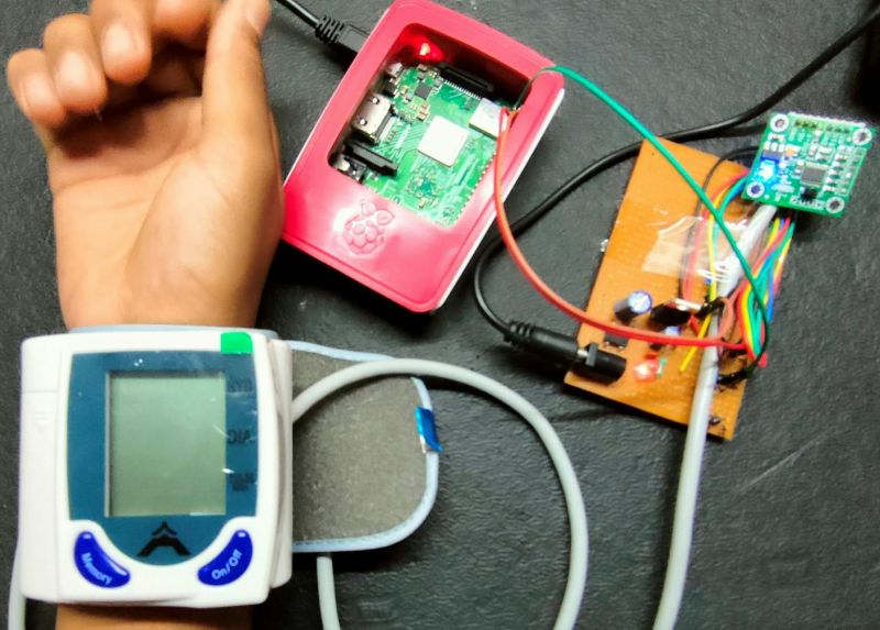
Blood pressure monitoring is a critical aspect of healthcare that has traditionally been confined to clinical settings or expensive home monitoring devices. With the advent of affordable single-board computers like the Raspberry Pi and accessible sensor technology, it’s now possible to create custom blood pressure monitoring systems for research, educational, and personal health tracking purposes.
The Raspberry Pi’s GPIO pins, analog-to-digital conversion capabilities, and robust software ecosystem make it an excellent platform for interfacing with various types of blood pressure sensors. This comprehensive guide will walk you through the process of connecting, programming, and implementing blood pressure monitoring systems using Raspberry Pi.
Understanding Blood Pressure Measurement
Before diving into the technical implementation, it’s essential to understand how blood pressure measurement works. Blood pressure is typically measured using two primary methods:
Oscillometric Method: This is the most common method used in automatic blood pressure monitors. It involves inflating a cuff around the arm and detecting oscillations in pressure as the cuff deflates. The maximum oscillation corresponds to mean arterial pressure, while systolic and diastolic pressures are calculated using algorithms.
Auscultatory Method: This traditional method involves listening to Korotkoff sounds through a stethoscope while manually deflating a cuff. While more accurate when performed correctly, it’s difficult to automate.
For Raspberry Pi implementations, the oscillometric method is more practical due to its ability to be fully automated through pressure sensors and pneumatic control systems.
Types of Blood Pressure Sensors
Pressure Transducers
Piezoelectric Sensors: These sensors convert mechanical pressure into electrical signals. They’re highly sensitive and can detect minute pressure changes, making them suitable for blood pressure monitoring applications.
Strain Gauge Sensors: These sensors measure pressure by detecting deformation in a diaphragm. They offer good linearity and stability over temperature variations.
Capacitive Pressure Sensors: These sensors measure pressure through changes in capacitance. They provide excellent sensitivity and are less susceptible to electromagnetic interference.
Recommended Sensors for Raspberry Pi
MPX5700AP: A popular choice for DIY blood pressure monitors, this sensor provides 0-700 kPa pressure range with excellent linearity and temperature compensation.
BMP280/BME280: While primarily designed for atmospheric pressure, these sensors can be adapted for blood pressure applications with proper amplification circuits.
Honeywell 24PC Series: Professional-grade pressure sensors with excellent accuracy and stability, suitable for medical-grade applications.
Hardware Requirements and Setup
Essential Components
Raspberry Pi (3B+ or 4 recommended for processing power)
The blood pressure monitoring system requires careful circuit design to ensure accurate pressure measurement and safe operation.
Pressure Sensor Connection: The MPX5700AP sensor typically outputs 0.2V to 4.8V corresponding to 0-700 kPa. This signal needs to be conditioned and converted to digital format using the MCP3008 ADC.
Connect the pressure sensor’s output to an operational amplifier configured as a non-inverting amplifier to boost the signal and provide impedance matching. The amplified signal then connects to one of the MCP3008’s analog input channels.
MCP3008 ADC Wiring:
VDD and VREF to 3.3V
AGND and DGND to ground
CLK to GPIO 11 (SCLK)
DOUT to GPIO 9 (MISO)
DIN to GPIO 10 (MOSI)
CS to GPIO 8 (CE0)
Pneumatic System Control: The air pump connects to a 12V power supply through a relay controlled by a GPIO pin. The solenoid valve similarly connects through another relay for controlled pressure release.
Software Implementation
Setting Up the Raspberry Pi Environment
Begin by updating your Raspberry Pi and installing necessary libraries:
Create a Python class to handle pressure sensor communication:
python
import spidev
import time
import numpy as np
from scipy import signal
import RPi.GPIO as GPIO
class BloodPressureMonitor:
def __init__(self):
self.spi = spidev.SpiDev()
self.spi.open(0, 0) # Bus 0, Device 0
self.spi.max_speed_hz = 1000000
# GPIO setup for pump and valve control
GPIO.setmode(GPIO.BCM)
GPIO.setup(18, GPIO.OUT) # Pump control
GPIO.setup(19, GPIO.OUT) # Valve control# Calibration constants
self.pressure_offset = 0.2 # Sensor offset voltage
self.pressure_scale = 4.6 # Voltage range
self.max_pressure = 700 # kPa
def read_pressure(self, channel=0):
"""Read pressure from ADC channel"""
adc = self.spi.xfer2([1, (8 + channel) << 4, 0])
data = ((adc[1] & 3) << 8) + adc[2]
voltage = (data * 3.3) / 1024
# Convert voltage to pressure (kPa)
pressure = ((voltage - self.pressure_offset) /
self.pressure_scale) * self.max_pressure
return max(0, pressure) # Ensure non-negative pressure
def control_pump(self, state):
"""Control air pump"""
GPIO.output(18, state)
def control_valve(self, state):
"""Control release valve"""
GPIO.output(19, state)
Oscillometric Algorithm Implementation
The core of blood pressure measurement lies in the oscillometric algorithm that analyzes pressure oscillations during cuff deflation:
python
def measure_blood_pressure(self):
    """Complete blood pressure measurement cycle"""
    pressures = []
    oscillations = []

    # Inflation phase
    print("Inflating cuff...")
    self.control_pump(True)
    self.control_valve(False)

    while True:
        current_pressure = self.read_pressure()
        pressures.append(current_pressure)

        if current_pressure > 180:  # Target pressure (mmHg equivalent)
            break
        time.sleep(0.1)

    self.control_pump(False)

    # Deflation and measurement phase
    print("Measuring oscillations...")
    self.control_valve(True)  # Slow release

    measurement_data = []
    for _ in range(300):  # 30 seconds at 10Hz
        pressure = self.read_pressure()
        measurement_data.append(pressure)
        time.sleep(0.1)

    self.control_valve(False)

    # Signal processing for oscillation detection
    filtered_signal = self.apply_bandpass_filter(measurement_data)
    envelope = self.extract_envelope(filtered_signal)

    # Calculate blood pressure values
    systolic, diastolic, map_pressure = self.calculate_bp(
        measurement_data, envelope)

    return systolic, diastolic, map_pressure

def apply_bandpass_filter(self, data, low_freq=0.5, high_freq=5.0, fs=10):
    """Apply bandpass filter to isolate oscillations"""
    nyquist = fs / 2
    low = low_freq / nyquist
    high = high_freq / nyquist

    b, a = signal.butter(4, [low, high], btype='band')
    filtered_data = signal.filtfilt(b, a, data)
    return filtered_data

def extract_envelope(self, oscillation_data):
    """Extract envelope of oscillation signal"""
    analytic_signal = signal.hilbert(oscillation_data)
    envelope = np.abs(analytic_signal)
    return envelope

def calculate_bp(self, pressure_data, envelope):
    """Calculate systolic and diastolic pressure"""
    # Find maximum oscillation amplitude
    max_amplitude_idx = np.argmax(envelope)
    max_amplitude = envelope[max_amplitude_idx]

    # MAP corresponds to maximum oscillation
    map_pressure = pressure_data[max_amplitude_idx]

    # Systolic: pressure at 50% of max amplitude (rising)
    threshold_50 = max_amplitude * 0.5
    threshold_70 = max_amplitude * 0.7

    # Find systolic pressure (before maximum)
    for i in range(max_amplitude_idx):
        if envelope[i] >= threshold_50:
            systolic = pressure_data[i]
            break

    # Find diastolic pressure (after maximum)
    for i in range(max_amplitude_idx, len(envelope)):
        if envelope[i] <= threshold_70:
            diastolic = pressure_data[i]
            break

    return systolic, diastolic, map_pressure
Data Processing and Calibration
Signal Conditioning
Raw pressure sensor data requires significant processing to extract meaningful blood pressure values. The signal conditioning pipeline includes:
Noise Filtering: Implement digital filters to remove electrical noise and mechanical vibrations that can interfere with pressure measurements.
Baseline Correction: Account for atmospheric pressure variations and sensor drift by establishing a baseline reference.
Temperature Compensation: Many pressure sensors exhibit temperature sensitivity that must be compensated through calibration curves or active temperature monitoring.
Calibration Procedures
Accurate blood pressure measurement requires careful calibration against known pressure standards:
python
def calibrate_sensor(self):
    """Calibrate pressure sensor against known references"""
    reference_pressures = [0, 50, 100, 150, 200]  # mmHg
    measured_values = []

    for ref_pressure in reference_pressures:
        input(f"Set reference pressure to {ref_pressure} mmHg and press Enter...")
        readings = []
        for _ in range(10):
            readings.append(self.read_pressure())
            time.sleep(0.5)

        measured_values.append(np.mean(readings))

    # Calculate calibration coefficients
    coefficients = np.polyfit(measured_values, reference_pressures, 1)
    self.calibration_slope = coefficients[0]
    self.calibration_offset = coefficients[1]

    print(f"Calibration complete: slope={self.calibration_slope:.4f}, "
          f"offset={self.calibration_offset:.4f}")
Advanced Features and Optimization
Real-time Data Visualization
Implement real-time plotting to visualize pressure waveforms during measurement:
python
import matplotlib.pyplot as plt
import matplotlib.animation as animation

def setup_realtime_plot(self):
    """Setup real-time pressure monitoring"""
    self.fig, (self.ax1, self.ax2) = plt.subplots(2, 1, figsize=(10, 8))
    self.pressure_line, = self.ax1.plot([], [], 'b-')
    self.oscillation_line, = self.ax2.plot([], [], 'r-')

    self.ax1.set_title('Cuff Pressure')
    self.ax1.set_ylabel('Pressure (mmHg)')
    self.ax2.set_title('Oscillations')
    self.ax2.set_ylabel('Amplitude')

    self.time_data = []
    self.pressure_data = []
    self.oscillation_data = []

def animate_plot(self, frame):
    """Animation function for real-time plotting"""
    current_time = time.time()
    current_pressure = self.read_pressure()

    self.time_data.append(current_time)
    self.pressure_data.append(current_pressure)

    # Keep only last 30 seconds of data
    if len(self.time_data) > 300:
        self.time_data.pop(0)
        self.pressure_data.pop(0)

    # Update plots
    self.pressure_line.set_data(self.time_data, self.pressure_data)
    self.ax1.relim()
    self.ax1.autoscale_view()

    return self.pressure_line,
Data Logging and Storage
Implement comprehensive data logging for long-term monitoring and analysis:
python
import json
from datetime import datetime

def log_measurement(self, systolic, diastolic, map_pressure):
    """Log measurement data with timestamp"""
    measurement = {
        'timestamp': datetime.now().isoformat(),
        'systolic': systolic,
        'diastolic': diastolic,
        'map': map_pressure,
        'device_id': self.get_device_id()
    }

    with open('bp_measurements.json', 'a') as f:
        json.dump(measurement, f)
        f.write('\n')
Safety Considerations and Limitations
Medical Device Regulations
Important Disclaimer: Any blood pressure monitoring system built with Raspberry Pi is intended for educational and research purposes only. It should not be used for medical diagnosis or treatment decisions without proper validation and regulatory approval.
Safety Measures
Pressure Limiting: Implement multiple safety mechanisms to prevent excessive pressure that could cause injury:
Software pressure limits with automatic pump shutdown
Hardware pressure relief valves
Maximum inflation time limits
Electrical Safety: Ensure proper isolation between high-voltage pump circuits and low-voltage sensor circuits to prevent damage to the Raspberry Pi.
Accuracy Considerations
DIY blood pressure monitors face several accuracy challenges:
Sensor calibration drift over time
Temperature sensitivity
Mechanical coupling variations
Individual physiological differences
Regular calibration against clinical-grade devices is essential for maintaining measurement accuracy.
Future Enhancements and Applications
IoT Integration
Extend the system with wireless connectivity for remote monitoring:
WiFi-enabled data transmission to cloud platforms
Mobile app integration for real-time monitoring
Integration with electronic health record systems
Machine Learning Enhancement
Implement machine learning algorithms to improve measurement accuracy:
Personalized oscillometric algorithms
Artifact detection and rejection
Trend analysis for early warning systems
Multi-parameter Monitoring
Expand the system to monitor additional cardiovascular parameters:
Heart rate variability
Pulse transit time
Arterial stiffness indices
Conclusion
Interfacing blood pressure sensors with Raspberry Pi opens up exciting possibilities for custom health monitoring solutions. While the technical implementation requires careful attention to signal processing, calibration, and safety considerations, the result is a flexible platform for research, education, and prototype development.
The combination of affordable hardware, powerful software libraries, and open-source development tools makes it possible to create sophisticated monitoring systems that were previously only available in clinical settings. As sensor technology continues to improve and computational power increases, we can expect even more advanced capabilities in future implementations.
Remember that while these systems provide valuable learning opportunities and research platforms, they should complement, not replace, professional medical monitoring and should always be used with appropriate safety precautions and medical oversight.
The Internet of Things (IoT) has revolutionized how we collect and transmit data from remote locations, but traditional Wi-Fi and cellular connections often fall short in terms of range and power consumption. LoRaWAN (Long Range Wide Area Network) technology addresses these limitations by providing long-range, low-power wireless communication perfect for IoT applications. When combined with the versatile ESP32 microcontroller, you can create powerful sensor nodes capable of transmitting data over several kilometers while maintaining excellent battery life.
This comprehensive guide will walk you through building a complete ESP32 LoRaWAN node using the familiar Arduino IDE environment, covering everything from hardware selection to network deployment.
Understanding LoRaWAN Technology
LoRaWAN operates in unlicensed ISM bands and uses a star-of-stars topology where end devices communicate with gateways, which then forward data to network servers. The technology offers three device classes: Class A (lowest power, bidirectional), Class B (scheduled downlinks), and Class C (continuously listening, highest power consumption). For most sensor applications, Class A provides the optimal balance of functionality and power efficiency.
The protocol supports adaptive data rate (ADR), which automatically optimizes transmission parameters based on network conditions, and provides built-in security through AES encryption at multiple layers. LoRaWAN networks can support thousands of devices per gateway, making them ideal for smart city deployments, agricultural monitoring, and industrial IoT applications.
Hardware Requirements and Selection
Building a robust ESP32 LoRaWAN node requires careful component selection. The ESP32 serves as your main microcontroller, offering built-in Wi-Fi and Bluetooth capabilities alongside GPIO pins for sensor interfacing. Choose an ESP32 development board with sufficient flash memory (at least 4MB) and adequate GPIO pins for your specific application requirements.
For LoRa communication, you’ll need a compatible radio module. The Semtech SX1276/SX1278 chips are widely supported and offer excellent performance in the 868MHz (Europe) or 915MHz (North America) bands. Popular options include the RFM95W module or integrated boards like the Heltec WiFi LoRa 32, which combines the ESP32 and LoRa radio on a single PCB.
An appropriate antenna is crucial for achieving maximum range. A simple wire antenna cut to quarter-wavelength (approximately 8.2cm for 868MHz or 7.8cm for 915MHz) works for testing, but consider a proper external antenna for production deployments. Spring antennas or small PCB antennas offer good performance in compact form factors.
Power management components are essential for battery-operated nodes. A low-dropout voltage regulator ensures stable 3.3V supply, while a battery monitoring circuit helps track remaining capacity. Consider adding a solar charging circuit for remote installations requiring long-term autonomous operation.
Setting Up the Arduino IDE Environment
Begin by installing the latest version of Arduino IDE and adding ESP32 board support. Navigate to File > Preferences and add the Espressif board manager URL: https://dl.espressif.com/dl/package_esp32_index.json. Then open Tools > Board > Boards Manager, search for “ESP32,” and install the ESP32 board package.
Next, install the required libraries for LoRaWAN communication. The MCCI LoRaWAN LMIC library provides comprehensive LoRaWAN stack implementation optimized for Arduino environments. Install it through Library Manager by searching for “MCCI LoRaWAN LMIC library.” This library handles all protocol complexities, including message encryption, frequency hopping, and duty cycle management.
You’ll also need supporting libraries depending on your sensors and requirements. Common additions include the Adafruit Sensor library for standardized sensor interfaces, ArduinoJson for data formatting, and specific libraries for sensors like BME280 (temperature, humidity, pressure) or GPS modules.
Configure your board settings in Arduino IDE by selecting your specific ESP32 variant under Tools > Board. Set the upload speed to 921600 for faster programming, and ensure the correct COM port is selected. If using a board with integrated LoRa radio, verify the pin definitions match your hardware configuration.
Wiring and Circuit Design
Proper wiring ensures reliable communication between the ESP32 and LoRa module. If using separate modules, connect the SX1276/1278 radio to the ESP32 via SPI interface. Typical connections include: SCK to GPIO5, MISO to GPIO19, MOSI to GPIO27, NSS (chip select) to GPIO18, DIO0 to GPIO26, DIO1 to GPIO33, and RST to GPIO14. Verify these pin assignments match your specific hardware configuration.
Power connections require careful attention to avoid noise and ensure stable operation. Connect both modules to a clean 3.3V supply with appropriate decoupling capacitors (100nF ceramic and 10µF electrolytic) placed close to power pins. Include a common ground connection and consider adding ferrite beads on power lines to reduce EMI.
For battery-powered applications, implement proper power management circuits. A voltage divider allows monitoring battery voltage through an analog input, while a MOSFET switch can control power to sensors and peripherals, enabling deep sleep functionality for maximum battery life.
Antenna placement significantly impacts performance. Keep the antenna away from other components and metal objects, use proper ground plane design, and ensure good impedance matching. Consider adding ESD protection components if the antenna is externally accessible.
Programming the Basic LoRaWAN Node
Start with a minimal working example that establishes LoRaWAN connectivity. Configure the LMIC library with your region-specific parameters, including frequency plan, duty cycle restrictions, and maximum transmission power. Initialize the radio with proper pin definitions and configure the device keys for Over-The-Air Activation (OTAA).
Your main loop should handle sensor readings, data formatting, and transmission scheduling. Implement proper timing to respect duty cycle limitations and avoid overwhelming the network. A typical structure includes sensor reading functions, data packaging routines, and transmission state management.
Here’s a basic framework for the main program structure:
Implement robust error handling for network join failures, transmission errors, and sensor malfunctions. Add debugging output to monitor join status, signal strength, and transmission confirmations during development.
Network Integration and Device Provisioning
Before your device can communicate, it must be registered with a LoRaWAN network server. For development and testing, The Things Network (TTN) provides free community network access. Create an account, register your application, and add your device with the appropriate keys.
Configure your device for OTAA, which provides better security than Activation By Personalization (ABP). Generate unique DevEUI, AppEUI, and AppKey values for each device. The DevEUI should be globally unique (many modules include a pre-programmed EUI), while AppEUI identifies your application and AppKey provides encryption.
Set up payload decoders on the network server to convert your binary data into human-readable formats. Create a decoder function that matches your data structure, enabling proper visualization and integration with external platforms. Consider using standardized payload formats like Cayenne LPP for simplified integration.
Configure downlink handling if your application requires remote control or configuration updates. Implement proper message parsing and response mechanisms while considering the limited downlink opportunities in Class A devices.
Advanced Features and Optimization
Implement adaptive data rate (ADR) functionality to optimize transmission parameters automatically. ADR adjusts spreading factor and transmission power based on network feedback, improving overall network efficiency and extending device battery life.
Add comprehensive sensor integration with proper calibration and error handling. Implement sensor fusion for applications requiring multiple measurements, and consider adding local data processing to reduce transmission frequency and payload size.
Develop robust power management strategies for battery-operated deployments. Implement deep sleep modes between transmissions, disable unnecessary peripherals, and use wake-up timers or external interrupts for event-driven operation. Monitor battery voltage and implement low-battery warnings or emergency shutdown procedures.
Consider implementing data compression and intelligent sampling strategies to maximize information density while minimizing airtime usage. Use techniques like delta encoding for slowly changing values or implement local thresholds to transmit only significant changes.
Troubleshooting and Best Practices
Common issues include join failures, typically caused by incorrect keys, frequency configuration, or poor radio reception. Verify all parameters match your network server configuration and ensure adequate antenna performance. Use debug output to monitor join attempts and response timing.
Range issues often stem from antenna problems, interference, or inappropriate transmission parameters. Test with line-of-sight conditions first, then gradually introduce obstacles while monitoring signal strength and packet success rates.
Power consumption higher than expected usually indicates improper sleep implementation or sensors remaining active during idle periods. Use current measurement tools to identify power-hungry components and verify sleep mode operation.
Implement proper firmware update mechanisms for deployed devices, considering the challenges of remote access and limited downlink capacity. Design your update process to handle interrupted transfers and provide rollback capabilities.
Conclusion and Future Development
Building an ESP32 LoRaWAN node opens possibilities for countless IoT applications, from environmental monitoring to asset tracking. The combination of ESP32’s processing power and LoRaWAN’s long-range capabilities creates a powerful platform for distributed sensing networks.
Future enhancements might include edge computing capabilities, machine learning inference for local data processing, or integration with other wireless protocols for hybrid connectivity solutions. As LoRaWAN networks continue expanding globally, your ESP32 nodes can participate in increasingly sophisticated IoT ecosystems.
The foundation you’ve built provides a starting point for more complex applications. Consider exploring advanced features like multicast communications, Class B scheduling, or custom payload encryption for specialized security requirements. With proper design and implementation, your ESP32 LoRaWAN nodes can operate reliably for years, providing valuable data for decision-making and automation systems.
Remember that successful IoT deployments require careful planning of network coverage, device management, and data integration. Start with small pilot projects to validate your approach before scaling to larger deployments, and always consider the long-term maintenance and support requirements of your IoT infrastructure.
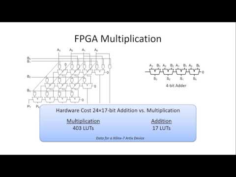
Field-Programmable Gate Arrays (FPGAs) have emerged as the preferred platform for high-performance digital signal processing (DSP) applications, offering a unique combination of flexibility, parallelism, and performance that traditional processors cannot match. Among the most fundamental DSP operations implemented on FPGAs, Finite Impulse Response (FIR) filters represent a critical building block that demands careful attention to timing optimization. As data rates continue to increase and latency requirements become more stringent, timing-driven design strategies have become essential for achieving optimal performance in FPGA-based FIR filter implementations.
The challenge of timing optimization in FPGA-based FIR filters extends beyond simple clock frequency considerations. Modern applications require designers to balance multiple competing objectives: maximizing throughput, minimizing latency, reducing resource utilization, and maintaining numerical accuracy. This multifaceted optimization problem necessitates sophisticated design strategies that leverage both architectural insights and implementation techniques specific to FPGA platforms.
FIR Filter Fundamentals and FPGA Implementation Challenges
FIR filters perform convolution operations between input samples and a set of predetermined coefficients, producing output samples according to the equation:
y[n] = Σ(k=0 to N-1) h[k] × x[n-k]
Where y[n] is the output sample, h[k] represents the filter coefficients, x[n-k] are the delayed input samples, and N is the filter length. While conceptually straightforward, implementing this operation efficiently on FPGAs presents several timing-related challenges.
The primary timing bottleneck in FIR filter implementations arises from the accumulation path, where partial products must be summed sequentially. In a naive implementation, the critical path would span multiple adder stages, limiting the achievable clock frequency. Additionally, the multiplication operations between input samples and coefficients can introduce significant propagation delays, particularly when using embedded multiplier blocks that may not be optimally placed relative to other logic elements.
FPGA-specific considerations further complicate timing optimization. Unlike ASICs, FPGAs have heterogeneous resources including dedicated DSP blocks, block RAMs, and configurable logic blocks, each with distinct timing characteristics. The routing architecture, while flexible, introduces variable delays that depend on the physical placement of logic elements. These factors necessitate design strategies that account for both algorithmic efficiency and platform-specific implementation details.
Architectural Design Strategies for Timing Optimization
Pipelining Techniques
Pipelining represents the most fundamental strategy for improving timing performance in FPGA-based FIR filters. By inserting registers at appropriate points in the datapath, designers can break long combinational paths into shorter segments, enabling higher clock frequencies. However, effective pipelining requires careful analysis of the computation structure to identify optimal pipeline boundaries.
Deep pipelining strategies involve inserting registers within individual multiply-accumulate operations, creating fine-grained pipeline stages. This approach is particularly effective for high-order filters where the accumulation chain would otherwise dominate the critical path. The trade-off is increased latency and register utilization, which must be balanced against the timing benefits.
Retiming techniques can further optimize pipelined implementations by redistributing registers to achieve better timing balance across pipeline stages. Modern synthesis tools provide automated retiming capabilities, but manual intervention is often necessary to achieve optimal results, particularly when dealing with complex filter structures or resource constraints.
Parallel Processing Architectures
Parallel processing offers another powerful approach to timing optimization, particularly for applications with high throughput requirements. The most common parallel architectures for FIR filters include:
Transposed Direct Form: This architecture parallelizes the multiply-accumulate operations by implementing them as separate multiply-add chains. Each coefficient multiplication occurs in parallel, with the results combined through a tree of adders. This approach eliminates the sequential accumulation bottleneck but requires additional multiplier resources.
Polyphase Decomposition: For decimation or interpolation filters, polyphase decomposition allows the filter to be partitioned into multiple parallel sub-filters operating at reduced sample rates. This technique not only improves timing by reducing the effective computation rate but also enables efficient resource utilization through time-multiplexing.
Systolic Array Implementations: Systolic arrays provide a highly regular architecture suitable for FPGA implementation. These structures feature short, identical connections between processing elements, enabling predictable timing characteristics and efficient routing utilization.
Coefficient Optimization Strategies
The choice and representation of filter coefficients significantly impact timing performance. Several optimization strategies can be employed:
Canonical Signed Digit (CSD) Representation: CSD encoding minimizes the number of non-zero digits in coefficient representation, reducing the complexity of multiplier implementations. This technique is particularly beneficial when implementing multipliers using shift-and-add structures rather than dedicated DSP blocks.
Coefficient Symmetry Exploitation: Many FIR filters exhibit symmetric or anti-symmetric coefficient patterns. Exploiting this symmetry can reduce the number of required multiplications by approximately half, with minimal timing overhead for the additional summation operations.
Dynamic Range Optimization: Analyzing the dynamic range requirements of intermediate computations allows for word-length optimization that can improve timing by reducing multiplier and adder complexities while maintaining acceptable numerical performance.
Implementation-Level Timing Optimization
Resource Mapping and Allocation
Effective utilization of FPGA resources is crucial for achieving optimal timing performance. Modern FPGAs provide dedicated DSP blocks optimized for multiply-accumulate operations, offering superior timing characteristics compared to equivalent implementations using general-purpose logic. However, these resources are limited and must be allocated judiciously.
The mapping of filter operations to DSP blocks requires consideration of the specific architecture of the target FPGA. For example, modern Xilinx UltraScale+ devices provide DSP48E2 blocks capable of performing complex multiply-accumulate operations with built-in pre-adders and post-adders. Utilizing these features effectively can eliminate additional logic requirements and improve overall timing.
Block RAM utilization for coefficient storage and delay line implementation also impacts timing performance. The timing characteristics of block RAMs depend on their configuration and access patterns. Optimizing these parameters while considering the overall system timing requirements is essential for achieving optimal performance.
Floorplanning and Placement Optimization
Physical placement of logic elements significantly affects timing performance in FPGA implementations. The routing delays between components can vary substantially based on their relative positions on the device. Strategic floorplanning can minimize these delays and improve timing predictability.
Clustering related logic elements in proximity reduces routing delays and improves timing closure. For FIR filter implementations, this typically involves grouping multiply-accumulate operations and their associated control logic within local regions of the FPGA. Advanced placement constraints can guide synthesis and place-and-route tools to achieve better results.
Regional clock buffering strategies can also impact timing performance, particularly in large filter implementations that span significant portions of the FPGA fabric. Careful consideration of clock distribution and skew management ensures reliable operation at high frequencies.
Advanced Timing Closure Techniques
When standard optimization techniques are insufficient to meet timing requirements, advanced closure strategies may be necessary:
Multi-Cycle Path Constraints: Some signal paths in FIR filter implementations may not require single-cycle timing, particularly in control or configuration paths. Identifying and constraining these paths appropriately prevents them from limiting overall performance.
False Path Analysis: Complex filter implementations may contain logic paths that are never exercised during normal operation. Identifying and constraining these false paths eliminates unnecessary timing restrictions.
Clock Domain Crossing Optimization: Multi-rate filter implementations often require careful management of clock domain crossings. Proper synchronization techniques and timing constraints ensure reliable data transfer while minimizing impact on overall performance.
Case Studies and Performance Analysis
Practical implementation of timing-driven FIR filter design strategies demonstrates their effectiveness across various application scenarios. Consider a 128-tap FIR filter targeting a Xilinx UltraScale+ FPGA with a 500 MHz operating frequency requirement.
A baseline direct-form implementation typically achieves approximately 200 MHz due to the long accumulation chain. Applying deep pipelining with 8 pipeline stages improves performance to 350 MHz but increases latency to 8 clock cycles. Further optimization through transposed direct-form architecture with coefficient optimization achieves the target 500 MHz frequency while reducing latency to 3 cycles.
Resource utilization analysis reveals trade-offs between timing performance and implementation efficiency. The optimized implementation requires 64 DSP blocks compared to 128 in the baseline, demonstrating the effectiveness of architectural optimization in achieving better resource efficiency alongside improved timing.
Power consumption analysis shows that timing-optimized implementations often consume less power despite higher operating frequencies, due to reduced logic depth and improved resource utilization efficiency.
Future Directions and Emerging Techniques
Emerging FPGA architectures continue to evolve, offering new opportunities for timing optimization. AI-enhanced design tools are beginning to provide automated optimization capabilities that can identify non-obvious timing improvement opportunities. Machine learning approaches to placement optimization show promise for achieving better timing closure with reduced manual intervention.
Adaptive filter implementations that can modify their characteristics in real-time present new timing challenges and opportunities. These systems require careful consideration of reconfiguration timing and the impact of dynamic parameter changes on overall system timing.
Conclusion
Timing-driven FIR filter design for FPGAs requires a comprehensive approach that spans algorithmic optimization, architectural design, and implementation-level techniques. Success depends on understanding the interplay between filter requirements, FPGA resource characteristics, and timing constraints. As FPGA capabilities continue to advance and application requirements become more demanding, these design strategies will remain essential for achieving optimal performance in high-speed DSP applications.
The evolution toward more sophisticated timing optimization techniques, combined with improved design tools and methodologies, promises to further enhance the capabilities of FPGA-based DSP systems. Designers who master these timing-driven strategies will be well-positioned to leverage the full potential of FPGA platforms for next-generation signal processing applications.
The Internet of Things (IoT) has revolutionized how we collect, process, and analyze data from connected devices. For makers and developers working with Arduino platforms, integrating sensor data with robust storage and analytics solutions can significantly enhance project capabilities. The Arduino Yun, with its unique combination of microcontroller and Linux-based system, paired with QNAP’s QIoT Suite Lite, creates a powerful IoT ecosystem that enables seamless data collection, storage, and visualization.
Understanding the Components
The Arduino Yun represents a significant evolution in the Arduino family, featuring both an ATmega32u4 microcontroller and an Atheros AR9331 processor running OpenWrt Linux. This dual-processor architecture allows the device to handle sensor interfacing on the microcontroller side while managing network communications and data processing through the Linux environment. The built-in WiFi and Ethernet connectivity make it ideal for IoT applications requiring reliable network communication.
QNAP’s QIoT Suite Lite transforms compatible QNAP NAS devices into comprehensive IoT platforms. This software suite provides MQTT broker functionality, data visualization through dashboards, rule engine capabilities, and robust data storage options. The integration eliminates the need for separate cloud services while maintaining complete control over your data infrastructure.
Prerequisites and Setup Requirements
Before beginning the integration process, ensure you have the necessary hardware and software components. You’ll need an Arduino Yun with the latest firmware, a compatible QNAP NAS device running QTS 4.3.0 or later, and stable network connectivity for both devices. The QNAP NAS should have QIoT Suite Lite installed and configured, which can be downloaded from the QNAP App Center.
Network configuration plays a crucial role in successful integration. Both the Arduino Yun and QNAP NAS should be connected to the same local network, whether through WiFi or Ethernet connections. Document the IP addresses of both devices, as these will be essential for establishing communication protocols.
Installing and Configuring QIoT Suite Lite
Begin by accessing your QNAP NAS through the web interface and navigate to the App Center. Search for QIoT Suite Lite and install the application. Once installed, launch QIoT Suite Lite and complete the initial configuration wizard. This process includes setting up the MQTT broker, which serves as the communication hub between your Arduino Yun and the NAS.
During MQTT broker configuration, you’ll establish connection parameters including port numbers, authentication credentials, and security settings. The default MQTT port is 1883, but you can modify this based on your network requirements. Create dedicated user accounts for your Arduino devices to maintain security and enable proper access control.
Configure the data storage settings within QIoT Suite Lite to determine how sensor data will be stored and retained. The suite supports various storage options, including time-series databases optimized for IoT data patterns. Set appropriate retention policies based on your project requirements and available storage capacity.
Preparing the Arduino Yun
The Arduino Yun requires specific libraries and configurations to communicate effectively with QIoT Suite Lite. Install the necessary MQTT libraries through the Arduino IDE Library Manager, including PubSubClient for MQTT communication and Bridge library for Arduino-Linux communication.
Configure the network settings on your Arduino Yun to ensure reliable connectivity. This involves setting up WiFi credentials or Ethernet configuration depending on your preferred connection method. Test the network connectivity using simple ping commands or web requests to verify proper communication.
Develop a basic sketch that initializes the MQTT connection and establishes communication with the QIoT Suite Lite broker. The sketch should include connection retry logic to handle temporary network interruptions and maintain reliable data transmission.
Establishing MQTT Communication
MQTT (Message Queuing Telemetry Transport) serves as the primary communication protocol between the Arduino Yun and QIoT Suite Lite. This lightweight, publish-subscribe protocol is ideal for IoT applications due to its efficiency and reliability in low-bandwidth environments.
Create MQTT topics that organize your sensor data logically. Use hierarchical topic structures such as “home/sensors/temperature” or “greenhouse/humidity/sensor1” to enable easy data filtering and routing. Consistent topic naming conventions facilitate dashboard creation and data analysis within QIoT Suite Lite.
Implement proper error handling and connection management in your Arduino code. Include functions to detect connection failures, attempt reconnections, and buffer data during temporary outages. This ensures data integrity and minimizes information loss during network disruptions.
Sensor Integration and Data Collection
With the communication framework established, integrate various sensors with your Arduino Yun to collect meaningful environmental data. Common sensors include temperature and humidity sensors (DHT22), light sensors (LDR), motion detectors (PIR), and air quality sensors. Each sensor requires appropriate libraries and calibration procedures to ensure accurate readings.
Structure your sensor data in JSON format for transmission to QIoT Suite Lite. This standardized format enables easy parsing and processing within the NAS environment. Include timestamps, sensor identifiers, and measurement units to provide context for the collected data.
Implement sampling strategies that balance data frequency with network efficiency. High-frequency sampling may overwhelm network resources, while low-frequency sampling might miss critical events. Consider implementing adaptive sampling rates based on data variability or threshold-triggered reporting for optimal performance.
Creating Dashboards and Visualizations
QIoT Suite Lite provides powerful dashboard creation tools that transform raw sensor data into meaningful visualizations. Access the dashboard builder through the web interface and create custom widgets displaying real-time and historical data from your Arduino Yun sensors.
Configure various chart types including line graphs for temperature trends, gauge displays for current readings, and alert indicators for threshold violations. Customize time ranges, data aggregation methods, and visual styling to create professional-looking dashboards suitable for monitoring and analysis.
Implement automated alerting systems that notify administrators when sensor readings exceed predetermined thresholds. Configure email notifications, SMS alerts, or webhook integrations to ensure prompt response to critical conditions.
Advanced Features and Automation
Leverage QIoT Suite Lite’s rule engine to create automated responses based on sensor data patterns. Develop rules that trigger actions when specific conditions are met, such as activating ventilation systems when temperature exceeds limits or sending alerts during security breaches.
Implement data analytics functions that identify trends, anomalies, and correlations within your sensor data. Use built-in statistical functions or export data to external analytics platforms for advanced processing and machine learning applications.
Configure data backup and synchronization features to protect against data loss and enable remote access to historical information. Set up automated backup schedules and configure cloud synchronization if required for off-site data protection.
Troubleshooting and Optimization
Common connectivity issues include network configuration problems, MQTT authentication failures, and firewall restrictions. Develop systematic troubleshooting procedures that verify network connectivity, test MQTT connections independently, and validate authentication credentials.
Monitor system performance metrics including network bandwidth utilization, storage consumption, and processing loads. Optimize data transmission frequencies and compression settings to maintain efficient operation while preserving data quality.
Implement logging and monitoring systems that track system health and identify potential issues before they impact data collection. Use QIoT Suite Lite’s built-in monitoring tools alongside custom logging solutions for comprehensive system oversight.
Security Considerations and Best Practices
Implement robust security measures to protect your IoT infrastructure from unauthorized access and data breaches. Use strong authentication credentials, enable SSL/TLS encryption for MQTT communications, and regularly update firmware on all connected devices.
Configure network segmentation to isolate IoT devices from critical network infrastructure. Implement firewall rules that restrict unnecessary network access while maintaining required communication paths between the Arduino Yun and QNAP NAS.
Establish regular maintenance schedules that include security updates, credential rotation, and system health checks. Document all configuration changes and maintain backup copies of critical settings to enable rapid recovery from system failures.
The integration of Arduino Yun with QNAP’s QIoT Suite Lite creates a powerful, self-contained IoT platform that enables sophisticated sensor data collection, storage, and analysis. This combination provides the flexibility of Arduino development with the robustness of enterprise-grade storage and analytics capabilities, making it ideal for both educational projects and professional IoT deployments.
Introduction: The Revolution of High-Frequency Sensing
In the rapidly evolving landscape of sensor technology, Millimeter WaveRadar has emerged as a transformative force, redefining precision sensing across multiple industries. Operating in the frequency range of 30–300 GHz with a wavelength of 1–10 mm, millimeter wave radar is characterized by its small size, lightweight, high spatial resolution, and strong ability to penetrate fog, smoke, and dust. This advanced sensing technology has become indispensable for applications ranging from automotive safety systems to industrial automation, medical diagnostics, and beyond.
The significance of millimeter wave radar extends far beyond its technical specifications. The millimeter wave radar market size was USD 10.2 billion in 2024 and is anticipated to reach a valuation of USD 202.9 billion by the end of 2037, rising at a CAGR of 26.1%, demonstrating the technology’s unprecedented growth trajectory and market confidence.
Understanding Millimeter Wave Radar Technology
Fundamental Principles and Operation
Millimeter wave (mmWave) radar utilizes frequency bands, such as 24 GHz, 60 GHz, and 77–79 GHz, to transmit and receive signals, delivering high-resolution measurements of distance, velocity, and angle. The technology operates on the principle of radio detection and ranging (radar), where electromagnetic waves are transmitted toward targets and analyzed upon reflection.
The core components of a millimeter wave radar system include a transmitting antenna, receiving antenna, and sophisticated signal processing units. The mmWave radar system includes a transmitting antenna, a receiving antenna, and a signal processing system to determine an object’s dynamic information, such as range, velocity, and angle of arrival (AoA). The system transmits millimeter wave signals into space, which reflect off objects and return to the receiving antenna. These echo signals are then processed to extract critical information about target objects.
Key Technical Advantages
The shorter wavelengths of millimeter wave radar provide several distinct advantages over conventional radar systems. The short 1–10 mm wavelengths enable fine spatial detail for detecting small objects and movements, allowing for unprecedented precision in object detection and classification.
Superior Resolution Capabilities: Millimeter wavelengths are well suited to the detection of certain types of targets that present a maximum radar cross-section (RCS), especially cables: electrical cables, cable car lines, etc. Centimeter-wave radars are only able to detect cables when reflection is specular, while millimeter-wave radars can detect them over a very wide angle.
Environmental Resilience: Millimeter wave radar performs consistently in challenging conditions such as darkness, smoke, dust, or fog, where optical sensors often fail. This reliability makes it invaluable for applications requiring consistent performance across diverse environmental conditions.
Privacy Protection: mmWave radar detects motion, presence, or respiration without capturing images—making it ideal for privacy-sensitive environments. This non-invasive characteristic has opened new applications in healthcare, smart buildings, and personal monitoring systems.
Frequency Bands and Spectrum Utilization
24 GHz Band Applications
The 24 GHz frequency band serves as an entry-level option for many millimeter wave radar applications. While offering good performance for basic sensing tasks, this band has certain limitations in resolution and bandwidth compared to higher frequency alternatives. However, it remains popular for cost-sensitive applications and regions with specific regulatory requirements.
60 GHz Band: The Sweet Spot for Short-Range Applications
The 60 GHz mm radar has a benefit of up to 7 GHz, especially for short-range applications, to provide better resolution. This frequency band has gained significant traction in industrial applications, smart home devices, and consumer electronics.
The 60GHz millimeter wave radar chip market was valued at 146 million in 2024 and is projected to reach US$ 714 million by 2032, at a CAGR of 25.7%. The rapid growth reflects increasing adoption across multiple sectors, particularly in automotive safety systems and IoT applications.
77-81 GHz Band: The Automotive Standard
The 77-81 GHz frequency band has become the gold standard for automotive applications. 77 GHz millimeter wave radar picked up 24GHz gradually from the market, becoming mainstream in the automotive field. This band offers an optimal balance of resolution, range, and regulatory approval across global markets.
79 GHz: Next-Generation Performance
The 79 GHz frequency band represents the latest advancement in automotive radar technology, offering even higher resolution and range capabilities compared to the 77 GHz band. This frequency band is particularly beneficial for applications that require ultra-high resolution, such as high-speed autonomous driving and complex traffic scenarios.
300 GHz and Beyond: Pushing the Boundaries
Research and development efforts continue to explore higher frequency bands, with 300 GHz radar systems providing bandwidth of more than 40 GHz leading to a range resolution of a few millimeters. These ultra-high frequency systems represent the cutting edge of millimeter wave radar technology, offering unprecedented precision for specialized applications.
Applications Across Industries
Automotive Sector: The Primary Driver
The automotive industry represents the largest and most rapidly growing market for millimeter wave radar technology. The global vehicle millimeter wave radar market was valued at USD 13,810 million in 2024 and is projected to grow from USD 16,420 million in 2025 to USD 48,730 million by 2032, exhibiting a CAGR of 19.7%.
Advanced Driver Assistance Systems (ADAS): Millimeter wave radar serves as the backbone of modern ADAS implementations. The global ADAS market penetration is expected to reach over 40% in new vehicle shipments by 2025, creating substantial growth opportunities for millimeter wave radar components. These systems provide critical safety features including adaptive cruise control, collision avoidance, blind spot detection, and automated emergency braking.
Autonomous Driving Technology: As the automotive industry progresses toward full autonomy, millimeter wave radar plays an increasingly vital role. High-level intelligent driving systems represented by urban NOA are facing more complex driving environments and roads, posing higher capability requirements for the perception system, requiring it to provide a longer detection range, a wider detection angle, and a higher accuracy.
4D Imaging Radar: The latest advancement in automotive radar technology introduces the concept of 4D imaging. Compared with 3D radar, 4D radar (distance, speed, horizontal azimuth, vertical height) provides point cloud functions by increasing the number of transmitting and receiving channels. This technology enables more detailed environmental mapping and improved object classification.
Industrial Automation and Manufacturing
Industrial automation represents one of the fastest-growing segments for 60GHz millimeter wave radar chips, with annual growth rates exceeding 28%. These chips enable precise object detection, level measurement, and vibration monitoring in harsh industrial environments where optical sensors often fail.
The technology’s ability to operate reliably in challenging industrial conditions makes it ideal for quality control systems, automated assembly lines, and process monitoring applications. The mmWave Technology based Industrial RoMs (AoPCB) come with SDK 3.05, along with object detection and counting sample applications.
Healthcare and Medical Applications
The healthcare sector has embraced millimeter wave radar for its non-contact monitoring capabilities. In February 2024, Infineon, FINGGAL LINK, and NEXTY Electronics announced a collaboration to develop an elderly safety monitoring system using 60 GHz millimeter-wave radar. This system enables non-contact monitoring of crucial health metrics like presence, respiration, heart rate, sleep patterns, and urinary incontinence, even through clothing.
Defense and Security Applications
Millimeter wave radar is used in short-range fire-control radar in tanks and aircraft, and automated guns (CIWS) on naval ships to shoot down incoming missiles. The small wavelength of millimeter waves allows them to track the stream of outgoing bullets as well as the target, allowing the computer fire control system to change the aim to bring them together.
The defense sector continues to invest heavily in millimeter wave radar technology. In October 2024, the U.S. Department of Defense awarded Raytheon Technologies a contract aimed at developing advanced millimeter wave radar systems with potential use in enhancing surveillance and reconnaissance operations.
Smart Cities and Infrastructure
Smart city infrastructure projects are incorporating vehicle-to-infrastructure (V2I) communication systems that utilize millimeter wave technology for traffic management and collision prevention. These applications demonstrate the technology’s versatility beyond traditional sensing applications.
Market Dynamics and Growth Drivers
Regulatory Mandates and Safety Standards
Government regulations worldwide are driving millimeter wave radar adoption. Government mandates like the NHTSA’s requirement for automatic emergency braking (AEB) in all light-duty vehicles by 2025 are pushing OEMs to integrate 77 GHz radar systems for superior resolution and range.
Europe leads in regulatory-driven adoption of millimeter wave radar, with EU General Safety Regulation (GSR) mandating features like intelligent speed assistance and lane-keeping systems. These regulatory frameworks create a stable foundation for market growth and technology investment.
Technological Advancements and Integration
Recent developments in chipset integration have reduced form factors while increasing accuracy, with some industrial-grade chips now achieving sub-millimeter measurement precision – a key requirement for quality control systems in precision manufacturing.
Regional Market Leadership
Asia-Pacific leads in market growth due to expanding automotive production in China and Japan, while Europe maintains technological leadership. China mandating radar-based safety features in 60% of new vehicles by 2025 as part of its Intelligent Connected Vehicle (ICV) development strategy demonstrates the region’s commitment to advanced automotive safety technologies.
Leading Industry Players and Competitive Landscape
Market Leaders
Bosch dominates the market with approximately 22% revenue share in 2024, leveraging its comprehensive ADAS solutions and strong OEM relationships across Europe and Asia. Other major players include Continental, Denso, Valeo, and Aptiv, each contributing unique technologies and solutions to the market.
Emerging Technology Companies
The market also features numerous emerging companies focusing on specialized applications and breakthrough technologies. From January to July 2024, domestic radar suppliers have begun to enter the supply chain systems of more OEMs in the fields of front radars (including 4D radar) and corner radars (including 4D radar), scrambling for bigger market share.
Strategic Partnerships and Collaborations
Key players like Infineon, Texas Instruments, and NXP are partnering with automotive OEMs and electronics firms to accelerate sensor commercialization. These partnerships are crucial for developing next-generation technologies and expanding market reach.
Technical Challenges and Solutions
Signal Processing Advancements
Signal processing advancements, including constant false alarm rate detection, multiple-input–multiple-output systems, and machine learning-based techniques, are explored for their roles in improving radar performance. These developments address fundamental challenges in target detection, false alarm reduction, and system reliability.
Manufacturing and Cost Optimization
Challenges such as complex manufacturing processes and regulatory constraints in certain regions may temper growth. However, ongoing improvements in semiconductor manufacturing and economies of scale continue to drive down costs while improving performance.
Miniaturization and Power Efficiency
Our latest mmWave sensors are designed from the ground up with low-power architecture to help you bring powerful radar sensing into applications that require lower power consumption in automotive, industrial, and consumer electronics applications. This focus on power efficiency enables new applications in battery-powered and portable devices.
Future Trends and Innovations
Integration with Artificial Intelligence
Our artificial intelligence-enabled, multi-functional radar sensors can replace multiple sensor technologies in a vehicle to reduce both cost and complexity of the system. The integration of AI and machine learning capabilities represents a significant advancement in millimeter wave radar technology.
Advanced Packaging Technologies
The antenna packaging technology is evolving from AoB to AiP (Antenna in Package), to reduce antenna feeder loss. A few companies such as Calterah have launched ROP (Radiator-on-Package) technology, which uses solder balls to connect RF signals, has higher channel isolation, and offers a longer detection range.
5G and Communication Integration
The ongoing rollout of 5G infrastructure is driving substantial investment in millimeter wave technologies, as network operators require semiconductor solutions capable of operating in the 24GHz to 100GHz range. This convergence of sensing and communication technologies opens new possibilities for integrated systems.
Emerging Applications
Automotive Applications Expansion: Growing adoption of 77 GHz and 79 GHz mmWave radar sensors in advanced driver assistance systems (ADAS) and autonomous vehicles. Consumer Electronics Integration: Companies are developing mmWave radar chips for gesture recognition, smart home automation, and human-computer interaction. Healthcare Innovation: Radar semiconductor sensors are being used in contactless monitoring of vital signs.
Technical Performance Characteristics
Resolution and Accuracy
High-range resolution is achieved by the radar, with examples showing range resolution capabilities down to 0.3 meters with bandwidth of 500 MHz at 94 GHz carrier frequency. These precision capabilities enable applications requiring millimeter-level accuracy.
Range and Detection Capabilities
With an output power of around 5 mW over the complete bandwidth, the system is mainly designed for short range applications up to several hundreds of meters. While some applications focus on short-range precision, others leverage millimeter wave radar for longer-range detection in automotive and aerospace applications.
Environmental Performance
In the range of millimeter wavelengths, the atmosphere offers several windows in which attenuation is not too high and where radar can operate. Understanding these atmospheric windows is crucial for optimizing system performance across different environmental conditions.
Implementation Considerations
System Integration
Complex signal processing runs within the mmWave RADAR Modules and only the processed Point Cloud RADAR data (Object’s ID, Range, Angle and Velocity) is given out over serial/CAN interfaces. This approach simplifies system integration while maintaining high performance.
Interface Standards
The millimeter wave radar modules support flexible industrial interfaces like USB, CAN, UART and SPI and can be powered via USB or Header. These standardized interfaces ensure compatibility with existing systems and facilitate rapid deployment.
Development Tools and Resources
Use our mmWave software development kit (SDK) and our mmWave studio to simplify your software development process. Comprehensive development ecosystems accelerate product development and reduce time-to-market for new applications.
Global Market Outlook and Regional Analysis
North American Market
The North American Vehicle Millimeter Wave Radar market is experiencing robust growth, driven by stringent safety regulations and accelerated ADAS adoption in the U.S. and Canada. The region benefits from strong R&D investments and established automotive manufacturing infrastructure.
European Market Leadership
Europe leads in regulatory-driven adoption of millimeter wave radar, with EU General Safety Regulation (GSR) mandating features like intelligent speed assistance and lane-keeping systems since recent regulatory implementations. The region’s focus on automotive safety and environmental regulations continues to drive market growth.
Asia-Pacific Growth
North America is expected to dominate the Millimeter Wave Radar Market over the forecast period, owing to the presence of major automotive and industrial automation companies in the region, while Asia-Pacific leads in market growth due to expanding automotive production in China and Japan. This regional dynamic reflects both established market leadership and emerging growth opportunities.
Investment and Development Trends
Corporate Investments
In March 2024, Avant Technology announced an investment of USD 100 million in an AI-centric data center in India to further consolidate its local data processing and millimeter wave radar capabilities. This facility is expected to be fully operational by 2025. Such investments demonstrate the industry’s commitment to expanding capabilities and market reach.
Research and Development Initiatives
An example of this can be seen in the collaboration of Keysight Technologies in March 2021 to establish a millimeter wave radar lab in Suzhou, China. This move promotes the development of technologies for autonomous driving and the better integration of mmWave radars into smart mobility solutions.
Challenges and Limitations
Technical Challenges
However, this absorption is maximum at a few specific absorption lines, mainly those of oxygen at 60 GHz and water vapor at 24 GHz and 184 GHz. At frequencies in the “windows” between these absorption peaks, millimeter waves have much less atmospheric attenuation and greater range. Understanding and working within these atmospheric limitations is crucial for optimal system design.
Regulatory and Standardization
The global nature of millimeter wave radar applications requires careful attention to regulatory requirements across different regions. Frequency allocation, power limits, and safety standards vary by country and application, necessitating careful system design and certification processes.
Cost and Manufacturing Complexity
While costs continue to decrease with improved manufacturing processes and economies of scale, the sophisticated technology still requires significant investment in design, testing, and production capabilities.
Future Outlook: The Next Decade of Millimeter Wave Radar
Market Growth Projections
The Millimeter Wave Radar Market is projected to grow from USD 3.63 billion in 2024 to USD 15.85 billion by 2034, at a CAGR of 15.89%. This substantial growth reflects the technology’s expanding role across multiple industries and applications.
Technological Evolution
The future trends in the Millimeter Wave Radar Market include the development of higher-resolution and longer-range millimeter wave radar sensors, the integration of millimeter wave radar technology with other sensor technologies, and the increasing use of millimeter wave radar technology in new applications such as healthcare and robotics.
Industry Transformation
The continued advancement of millimeter wave radar technology promises to transform industries beyond automotive and industrial applications. From smart cities to healthcare, from consumer electronics to space exploration, the precision sensing capabilities of millimeter wave radar will enable new applications and business models.
Conclusion: Shaping the Future of Precision Sensing
Millimeter Wave Radar technology represents a fundamental shift in precision sensing capabilities, operating in the 30-300 GHz spectrum to deliver unprecedented accuracy, reliability, and versatility. From its foundational role in automotive safety systems to its expanding applications in healthcare, industrial automation, and smart infrastructure, millimeter wave radar continues to push the boundaries of what’s possible in sensor technology.
The remarkable market growth projections, with valuations expected to reach hundreds of billions of dollars within the next decade, reflect not just market confidence but the genuine transformation this technology brings to diverse industries. As regulatory frameworks support adoption, manufacturing processes improve efficiency, and technological innovations expand capabilities, millimeter wave radar is positioned to become an essential component of our increasingly connected and automated world.
The journey from basic radar principles to today’s sophisticated millimeter wave systems demonstrates the power of continuous innovation and cross-industry collaboration. Looking ahead, the integration of artificial intelligence, advanced packaging technologies, and new frequency bands will further expand the potential applications and performance capabilities of this remarkable sensing technology.
As we advance toward an era of autonomous systems, smart cities, and precision healthcare, Millimeter Wave Radar stands as a cornerstone technology, enabling the precise sensing capabilities that will define the next generation of intelligent systems. The 30-300 GHz spectrum represents not just a range of frequencies, but a gateway to new possibilities in precision sensing and environmental understanding.
Creating a vibrant LED matrix display is one of the most rewarding electronics projects for beginners and experienced makers alike. Whether you choose Arduino or Raspberry Pi as your controller, building a colorful LED matrix opens up endless possibilities for creative displays, from scrolling text and animations to interactive games and ambient lighting. This comprehensive guide will walk you through everything you need to know to build your own stunning LED matrix display.
Understanding LED Matrices
An LED matrix is essentially a grid of light-emitting diodes arranged in rows and columns, allowing you to control individual pixels to create patterns, text, images, and animations. The most popular choices for DIY projects are WS2812B (NeoPixel) strips formed into matrices or dedicated LED matrix modules like the MAX7219-controlled panels.
The beauty of LED matrices lies in their addressability – each LED can be controlled independently for color and brightness. This pixel-level control enables you to create sophisticated visual effects with relatively simple programming. RGB LEDs add the color dimension, allowing you to display millions of different hues by mixing red, green, and blue components.
Choosing Your Platform: Arduino vs Raspberry Pi
Both Arduino and Raspberry Pi excel at controlling LED matrices, but each offers distinct advantages. Arduino microcontrollers provide real-time performance with predictable timing, making them ideal for smooth animations and precise color control. They’re also more power-efficient and cost-effective for dedicated display projects. Popular choices include the Arduino Uno, Nano, or ESP32 for WiFi connectivity.
Raspberry Pi computers offer more processing power and built-in networking capabilities, making them perfect for complex displays that need internet connectivity, multimedia playback, or advanced graphics processing. The Raspberry Pi can handle larger matrices and more sophisticated visual effects, while also running full applications like web servers or media players alongside your LED display.
Essential Components and Materials
For an Arduino-based matrix, you’ll need an Arduino board, a WS2812B LED strip (60 LEDs per meter works well), a 5V power supply capable of delivering sufficient current (approximately 60mA per LED at full brightness), jumper wires, and a breadboard or custom PCB. A 8×8 or 16×16 matrix makes an excellent starting size. You’ll also want a 470-ohm resistor for the data line and a 1000µF capacitor for power smoothing.
Raspberry Pi setups require similar components but benefit from the Pi’s built-in features. You’ll need a Raspberry Pi (3B+ or 4 recommended), microSD card, the same LED strips or matrix modules, appropriate power supply, and GPIO jumper wires. The Pi’s USB ports can power smaller matrices directly, though larger displays require external power supplies.
For both platforms, consider adding a push button or rotary encoder for user interaction, a real-time clock module for time-based displays, or sensors like temperature/humidity modules to create reactive displays that respond to environmental conditions.
Building Your Arduino LED Matrix
Start by planning your matrix layout. For a simple 8×8 matrix using WS2812B strips, cut your strip into 8 segments of 8 LEDs each. Arrange these strips in a serpentine pattern – the first row left-to-right, second row right-to-left, and so on. This creates a continuous data path while maintaining the logical matrix structure.
Solder the strips together carefully, connecting the data output of each row to the data input of the next. Create a sturdy backing using wood, acrylic, or 3D-printed frame to hold everything in place. Ensure proper spacing between LEDs for even light distribution and consider adding a diffusion layer using translucent plastic or fabric.
Wire the data input to Arduino pin 6, connect the power rails to your 5V supply, and establish a common ground between the Arduino and power supply. Install the 470-ohm resistor between the Arduino pin and the first LED’s data input to prevent signal integrity issues. Add the smoothing capacitor across the power rails near the LED strip.
Programming your Arduino requires the FastLED or Adafruit NeoPixel library. Here’s a basic framework that creates a simple animation:
The Raspberry Pi approach offers more flexibility with Python programming and built-in networking. Install the rpi_ws281x library, which provides excellent hardware-accelerated control of WS2812B strips. The wiring is similar to Arduino – connect your LED strip’s data line to GPIO 18 (pin 12), power to 5V, and establish common ground.
Python programming on the Pi allows for more complex effects and easier integration with web interfaces or external data sources. You can create displays that show weather information, social media feeds, or real-time data from APIs. The Pi’s processing power also enables more sophisticated graphics and smoother animations.
Here’s a Python foundation for your Pi-based matrix:
python
import time
from rpi_ws281x import PixelStrip, Color

LED_COUNT = 64
LED_PIN = 18
LED_FREQ_HZ = 800000
LED_DMA = 10
LED_BRIGHTNESS = 50

strip = PixelStrip(LED_COUNT, LED_PIN, LED_FREQ_HZ, LED_DMA, False, LED_BRIGHTNESS)
strip.begin()

def colorWipe(color, wait_ms=50):
    for i in range(strip.numPixels()):
        strip.setPixelColor(i, color)
        strip.show()
        time.sleep(wait_ms / 1000.0)
Advanced Programming Techniques
Both platforms support sophisticated visual effects through mathematical functions and algorithmic patterns. Implement functions to convert between matrix coordinates (x, y) and linear LED indices, accounting for your serpentine wiring pattern. This enables natural 2D graphics programming where you can draw shapes, text, and images intuitively.
Create reusable functions for common patterns like scrolling text, particle effects, and geometric animations. Consider implementing a frame buffer system that lets you draw an entire frame before displaying it, preventing visual artifacts during complex updates. For text display, create or import bitmap fonts that fit your matrix resolution.
Color management becomes crucial for professional-looking displays. Implement gamma correction to ensure linear brightness perception, and consider color temperature adjustment for different viewing environments. HSV color space often works better than RGB for creating smooth color transitions and animations.
Power Management and Safety
Power consumption is a critical consideration for LED matrices. Each LED can draw up to 60mA at full white brightness, so a 64-LED matrix might need nearly 4 amperes. Always calculate your power requirements and use appropriately rated supplies with safety margins. Implement software brightness limiting to prevent exceeding your power supply’s capabilities.
For portable projects, consider battery operation with power management features like automatic sleep modes and brightness adjustment based on ambient light. USB power banks work well for smaller matrices, while larger displays might need dedicated battery solutions with proper charging circuits.
Ensure all connections are secure and insulated to prevent short circuits. Use proper gauge wire for power distribution, and consider adding fuses or current-limiting circuits for additional safety. Heat dissipation becomes important for high-brightness operation or larger matrices.
Expanding Your Project
Once you have a basic matrix working, numerous enhancement opportunities await. Add touch sensors to create interactive displays that respond to user input. Integrate WiFi connectivity for internet-based information displays or remote control capabilities. Sound reactive displays using microphone modules create spectacular music visualizers.
Consider multiplexing techniques to drive larger matrices more efficiently, or chain multiple smaller matrices together for bigger displays. Real-time clock modules enable time-based displays, while environmental sensors create responsive ambient lighting that adapts to room conditions.
For advanced users, explore specialized LED driver chips like the MAX7219 for traditional matrix displays, or investigate newer technologies like addressable LED panels that provide higher pixel densities. FPGA-based controllers can drive extremely large displays with professional-grade performance.
Troubleshooting Common Issues
Signal integrity problems often manifest as incorrect colors or flickering, usually caused by inadequate power supply, loose connections, or interference. Ensure your data line connections are solid, use appropriate resistors, and keep data wires away from power lines to minimize noise.
Power-related issues typically show as LEDs dimming unexpectedly or displaying incorrect colors, especially at the end of long strips. This indicates voltage drop along the power distribution. Solution involves adding power injection points throughout your matrix or using thicker gauge wire for power distribution.
Timing issues in Arduino projects might cause erratic behavior, particularly when mixing LED control with other functions. Use non-blocking programming techniques and avoid delay() functions in main loops. For Raspberry Pi projects, ensure you’re running your LED control code with appropriate priority to maintain consistent timing.
Conclusion
Building a colorful LED matrix represents an perfect intersection of electronics, programming, and creative expression. Whether you choose Arduino for its real-time performance and simplicity, or Raspberry Pi for its processing power and connectivity, you’ll gain valuable experience in digital electronics, embedded programming, and project engineering.
Start with a simple 8×8 matrix to learn the fundamentals, then expand your projects as your skills and ambitions grow. The techniques you learn building LED matrices apply to countless other electronics projects, from wearable technology to large-scale installations. Most importantly, have fun experimenting with colors, patterns, and animations – the creative possibilities are truly limitless.