Zuken is a PCB design software mainly built to help in designing multi-chip modules and circuit boards. This software has been used in different applications which include wiring harness, electrotechnical engineering, etc.
Zuken has gained popularity in the PCB and engineering industry as it designs software for electrical and electronic engineering data management (e-PLM). The electronics industry is the main markets of Zuken. It specializes in the design of mobile communications devices, industrial equipment, construction machinery, digital home electrical appliances.
Also, you will find Zuken in other applications that include production of medical devices and automobile parts. With Zuken’s strong presence in the space and aviation sector, this company has been able to make huge impacts in these sectors through its products. Zuken is one of the best EDA companies that deals in the development of PCB design software. Other companies such as Mentor Graphics, Altium, and Cadence Design Systems also specialize in circuit board design software.
What are the Features of Zuken PCB Design Software?
PCB design engineers can integrate Zuken in their layout and schematics. This software has standard features to help you achieve a smooth workflow. In Zuken PCB design software, you will find excellent features like:
Schematic design and schematic capture
The process of circuit board design usually commences with schematic design. It prepares you ahead of the PCB design. Zuken provides industry-standard and exceptional schematic capture tools and schematic editors. The PCB schematics is an important aspect of PCB design which requires special tools to create.
Simulation and analysis tools
Zuken is a great platform that offers various simulation and analysis features for both digital and analog systems. It as well provides features for mixed-signal systems.
PCB layout
Another important thing you would benefit from using Zuken is its PCB layout features that helps you arrange components and as well route traces.
Production planning and BOM management
Every PCB design requires a schematic or more. To plan PCB manufacturing, you need Bills of Materials (BOM). Zuken has a standard BOM and generation tools to help you plan your PCB manufacturing process
What is Zuken CR5000?
This is an advanced PCB design software designed by Zuken. Zuken CR5000 is equipped with sophisticated features for laying out multilayer structures like IC packages and circuit boards. This integrated software provides lasting solutions for design issues like electromagnetic compatibility (EMC), power integrity, and signal integrity. Furthermore, Zuken CR5000 offers high-throughput manufacturing.
This Zuken‘s design suite for PCBs and electronics systems focuses at the enterprise market before CR-8000 was released in 2011. CR-5000 comes with a lot of integrated tools which offer the interactive workflow needed for an effective and clear design process. Also, these tools offer the technologies required for the successful development of electronics. These technologies include PCB design, constraints management, system design and analysis.
Also, CR5000 features PCB layout and verification, output manufacturing, and EMC. There are also additional features in CR500 which offer the smooth workflow needed for a successful design process. These additional features include effective documentation system, comprehensive parts library, and parts library manager. Also, Zuken enables co-verificatin and co-design with electrical and thermal design applications.
Other Features of Zuken CR5000
CR-5000 Library Tools
One of the amazing thing about CR5000 is that it integrates common library data all through the entire design cycle. These libraries are very easy to search and edit. Furthermore, there are tools needed for easy and fast component creation.
CR-5000 System Designer
Zuken CR5000 has a system designer. This is a sophisticated and industry-standard design solution for developing advanced electronic products. The system designer is an advanced graphical took used for analysis and design capture. Also, this tool offers support for various textual and graphical design entries. It is ideal for for both analog and digital signal circuit design at the PCB level.
The system designer tool is closely connected to verification, synthesis, debugging, simulation, and timing analysis all through the process of design. Furthermore, the design entry methodology can help in minimizing product size, design time, and product cost. It can as well enhance the product quality.
CR-5000 Board Designer
The CR5000 board designer by Zuken offer integrated environment for PCB and BGA design. Its user interface combines floorplanning, routing and placement, and schematic capture into manufacturing. These help in guiding the user.
Also, CR5000 board designer works seamlessly across platforms such as Windows and Unix by combining the functions of a sophisticated tool with ease of use. Although the rules are constant all through the process of design, these rules are connected to ensure a high level of flexibility and consistency.
Zuken created a Windows-based software that provides solutions to HDI PCBs and high speed layout. CADSTAR is a schematic and PCB design solution specially cretaed for high-speed PCB layout and High density interconnection (HDI). This solution has sophisticated PCB layout functions that help designers to seamlessly realize their design intent.
CADSTAR is an easy-to-use software that helps to reduce design errors and as well provide effective designs with less efforts and in less time.
CADSTAR is equipped with industrial-strength technology and as such, it features the capabilities required to address the design challenges being faced in the PCB and electronics industry. It is an affordable program that offers great functionality and performance.
CADSTAR has many satisfied users across the globe. As a professional and accessible software, CADSTAR is a great option for designers. It is optimized for both mid-sized and small design team.
Features and Benefits
Zuken CADSTAR can handle any design, regardless of its complexity.
It is a constraint-driven design that defines and integrate high-speed layouts.
CADSTAR comes with 3D-MCAD/ECAD integration.
The variant manager in CADSTAR enables a design to meet many target market or application requirements.
It features excellent performance and manufacturability.
CADSTAR is equipped with interactive and automatic placement and routing tools.
It comes with a various manufacturing formats.
This scalable design solution provides a high level of flexibility that can help you design complex circuit boards.
Conclusion
Zuken is a great platform for designing both simple and complex PCB designs. This software is available in other versions such as CR5000 and CR8000. Zuken is known for its advanced capabilities and benefits.
VFBGA basically stands for a very fine pitch array. It is something that many people might not have heard of before. But no worries. Since we are going to elaborate on this untouched topic for you in detail and see how the process works for real-world applications.
It is not like standard TFBGA packages; instead, it is much smaller in size. It also uses solder balls that are together in the form of a group.
These are mainly responsible for enhancing the electrical transmission throughout the system. By far, you must be getting the idea that VFBGA is suitable for congested solder balls. However, there is more to it. Let’s hop onto the next section on this note!
What Is VFBGA (Very Fine Pitch Ball Grid Array)?
You can define VFBGA as a small type of ball grid array that is so precise that it does not give you much margin for negligence and human error. The solder balls of VFBGA come in the form of a group that you can find under the integrated circuit. Well, a pretty difficult place to reach out, but solder balls work at their finest under the setup when you are considering VFBGA. So if you don’t forget this point, we shall move further in this discussion.
How Does VFBGA (Very Fine Pitch Ball Grid Array) Work?
As we have successfully described what VFBGA is, we need to shed some light on the working of this technology. We are not going to make it overwhelming for you, so let’s have a look at the following bullets to get a better understanding of how VFBGA works!
Here’s the thing, VFBGA has multiple coatings. One of them is the dielectric layer, the second is the solder mask, and the third comes for substrate material.
The substrate used for VFBGA if of clay which is highly important for stabilizing the base for integrated circuits since they can be short on performance later and we don’t want that.
The dielectric is for ensuring the protection of the conductive tracks present on the substrate
The solder mask is responsible for protecting the solder balls from one of their biggest foes, yes, tainting.
Now that you have learned about the individual roles of the layers of VFBGA, you need to know that the VFBGA package needs a reflow process to bolster solder connections.
You heat the solder balls until they melt like ice cream melts on a hot sunny day. So that they will contribute to solidifying the connections between the PCBs and their dedicated integrated circuits.
Features Of VFBGA (Very Fine Pitch Ball Grid Array)
· Fine Pitch
VFBGA bundles are fine, as you already know. Therefore, they serve best when you are talking about precise frequency that stays under 1milimeter. It comes in handy when you are working on increasing the density of integrated circuits for your setups. The high density mainly reduces the size and weight of devices, making them much more portable for users. So what makes VFBGA so fine to be a great fit for this purpose? It’s the latest cutting-edge process. It helps in maintaining a high pin count even if there is no large space present.
· High Pin-Count
Speaking of high pin count, if you don’t know it yet. Feel lucky as you are going to consume so much new information from this post for your next VFBGA project. Bear in mind that VFBGA packages always rely on a high pin count. Now, this pin count is important to impart different features to the bundles. Such as less number of components needed, more simplified wafers, and less weight.
· High-Speed Performance
The VFBGA bundles are not only responsible for making your devices easy to carry. But their speed and performance also owe to VFBGA bundles. It is important for quick data transmission between PCBs and their integrated circuits. Not just this, VFBGA goes deeper to the solder balls and also skyrockets their rate of transmission on the whole. High-speed performance devices matter extremely in the domains like consumer electronics and also telecommunication.
· Low Power Consumption
VFBGA is not going to let you down when you want to save the world by saving energy. Now how does VFBGA help your setups consume less power? Pretty logical! VFBGA bundles do not need much power because they are small in size. It means if you use them in a smart gadget, they will easily make it use less energy.
· High Reliability
VFBGA is reliable, and you should know this by now. No other technology can beat VFBGA for solidifying the solder connections. These connections, even between the PCBs and circuits, promise prolonged dependability just due to VFBGA.
Applications Of VFBGA (Very Fine Pitch Ball Grid Array)
· Consumer Electronics
Consumer electronics is a prominent use case of VFBGA. Devices like smartphones and gaming consoles are all existing due to this method. Just imagine you are playing a video game that is actually helping you consume less power and energy at the same time. Not just the portable nature of VFBGA needs your attention, but the quality of such devices remains consistent over the years as well.
· Telecommunications
Telecommunications devices like routers, modems, and consoles work on VFBGA. It is because entire telecommunication systems would just collapse if they were not quick and efficient. Guess what? VFBGA exactly makes this happen. It allows quick data transmission and forms precise networking between all the connected devices.
· Automotive
Automotive devices like Motor control units and ADAs all use VFBGA. It is because the efficiency of this technology, along with the less power consumption, makes it a perfect fit to develop such equipment.
· Industrial
VFBGA has vast applications in machine control frameworks, cycle mechanization, and mechanical tech. It is useful for modern gear because it works impressively even on less power and promises positive results.
The Final Say
It is not wrong to say that VFBGA is a driving force for so many industries around us. So many portable devices that we are using today all involve VFBGA in the core. Now that we have made you familiar with VFBGA by going in-depth, it’s time that you start considering to level-up your future assignments with VFBGA to make everyone rub their eyes out of surprise!
Before you do anything regarding planning your new circuit board layout, one thing you will have to do is designing the stackup as well as selecting your board’s material system. The circuit board laminate materials may seem simple. You believe it works like choosing your desired material and vendor, putting them in your stackup, then sending it to the fabricator.
The truth is that not every fabricator out there stock or support all the laminate materials possible. However there are some materials, which are compatible with themselves in the different stackups. Now, in what ways can you spot the resin system and materials that will be interchanged in the PCB stackup?
Enter the IPC standard IPC-4101 slash sheets. This standard helps in specifying the different requirements for the materials of the PCB laminate which helps in ensuring the compatibility and interchangeability in the PCB stackup. Though it is not required to read any slash sheets during the selection of materials, having understanding of what’s present in the slash sheet may assist you in determining the alternate materials when the desired laminates are not supported or available by the manufacturer.
Powered By EmbedPress
The Origin of the IPC 4101 Slash Sheet
Under IPC standards, the IPC 4101 slash sheets can be described as addenda which stats the requirements for the different laminates for the PCB stackups. The IPC 4101 standard utilized most of the initial languages from the MIL-S-13949 standard.
The slash sheets requirements for IPC 4101 persist till today and the laminate materials would list these slash sheets onto which the materials conform. If you check the website of a laminate manufacturer, or you check the datasheets of their laminate, you will most likely see something like “/24” or”/121” for some specific laminates. This refers to the IPC 4101 24 or IPC 4101/121 slash sheets respectively. Others include IPC 4101 126, IPC 4101 21, IPC 4101 26, and IPC 4101 41.
The slash sheet features two data sets on a specific material system. These are the material/primary structural properties, as well as some results for testing as determined using the IRC testing standard. In addition, any slash sheet begins with structural and material specifications for that specific laminate.
All manufacturers have their material names which aid in communicating the specific laminates onto the public and the customers. However, there will be a relationship between the laminates and the IPC 4101 standard. Below are some of the information you will find in slash sheets.
All flame retardants and filler materials available in the laminates
Tg or glass transition temperature
Resin material systems (which is usually an epoxy mix)
What is IPC 4101?
IPC 401 can be described as a specification for the base materials designed for multilayer and rigid printed circuit boards. It was released in December 1997. This came as a replacement for the MIL-S-13949 standard. Moreover, it had most of the same wording seen in the military standard.
Furthermore, its format appendix was maintained to a standard specifying the fiber and resin system of several PCB laminates, in addition to the properties and testing parameters. At first, 41 (forty-one) slash sheets were available; however, as the industry decided to work with “Green” and “Lead Free” processes, these slash sheets increased in number to sixty six (66).
With all these slash sheets, having a good understanding of what they are would offer great benefits to the choosing of the right properties of the laminate to suit your PCB design.
Laminate Specification of IPC 4101
All slash sheets start with a laminate specification. It involves the type of reinforcement, the resin system, the mechanism of the flame retardant, glass transition, and fillers. This type of reinforcement seems to be fiberglass (woven E-glass).
However, it could also be exotic fiberglass and cellulose paper types like aramid and unidirectional fiber. This serves as the laminate’s structure component. Also, resin systems could be a combination of different types of epoxies to meet the laminate type’s requirements. The main epoxy would be listed, after this, the secondary follows, and another secondary may even follow.
Utilizing Epoxy Resins
Some exotic resin systems like Polyphenylene and polyimide exist. This resin system binds the layers of the structure together. This flame retardant is usually RoHS compliant bromine or bromine, and phosphorus as another option as well. Fillers could be inorganic or not applicable, with just a few types of laminate making use of kaolin fillers. These fillers help in reducing resin shrinkage, therefore, reducing the formation of cracks in the filled areas.
Temperature of Glass Transition (Tg)
The temperature of glass transition describes the range of temperature whereby the resin’s molecules transits from its brittle and rigid state into its pliable and flexible state. The Tg was added to the area of specification because many designers decided to base their choice of laminate for compliance of RoHS on the Tg material. Asides from Several other factors which have to be considered during the selection of laminates.
Other Characteristics That You Must Be Aware of
The remaining slash sheet must list the requirements of the laminate for the material characteristics, which are tested for every IPC-TM-650 test method. Some of these features are highlighted below.
The peel strength helps in determining the metal cladding bond whenever it is tested after thermal stress, as well as after exposure to some processing chemicals
Absorption of moisture or moisture absorption helps in determining the absorption rate for that epoxy composite utilized in the structure of the laminate. Also, all the resin systems help in absorbing some moisture whenever it is exposed to a high humidity environment.
Surface and volume resistivity determines the surface and cross-sectional electrical resistance of a dielectric material when under some humid conditions.
Dielectric breakdown measures the ability of the insulator to withstand the high voltages stress that is placed across.
Loss Tangent can be described as a measure of the amount of electromagnetic field that travels through the dielectric is lost or absorbed in the dielectric
Also, you can determine flexural strength with laminates having a thickness of 0.51 mm or greater through the application of a load to a size as well as shaped specimen.
Thermal stress helps in determining the metallic clad or unclad laminates’ thermal integrity making use of short-term solder exposure.
Arc resistance measures the required time to make the insulating surface to be conductive when under low current and high voltage arc.
When searching for slash sheets from your laminate manufacturer, you may see both IPC 4101 and IPC 4103 standards. This IPC 4101 standard deals with the standard laminates as well as prepreg materials, thereby encompassing the materials of epoxy resin with fiberglass.
Though the standard initially specified a total of forty-one slash sheets, this number has increased to over sixty slash sheets. This is made possible by RoHS regulations as well as focus on the lead-free environmentally-friendly materials. This IPC-4102 also extends the slash sheets to the copper-unclad as and clad plastic laminate materials as well as bondply materials utilized in high frequency and high speed PCBs.
Calculate and Plan Your Stackup Early
Most, if not everyone, have a manufacturer that they prefer to use. With time, when you continue to order from one manufacturer, you will be very familiar with the materials as well as the stackups that they support.
Normally, this is listed by the laminate vendor number and name, instead of making use of slash sheet numbers. Moreover, there are fab houses that need you to specify the stackup you desire through a slash sheet. T5his is why it is important that this information is gotten from your own laminate manufacturer whenever you are submitting an order.
Preferred Circuit Board Stackups
Majority of manufacturers have stackups that they prefer, which are utilized for some layer counts and they are sure of passing through their process of fabrication. These stackups they prefer will feature some specific material systems. Make sure you work closely with the fabricator ensuring that your ideal stackup will be supported throughout the entire process
Where You Can Find Stackup Data
There are several fabrication houses that will place this online, while others will decide to email it to you. Whatever the case is, try to ask early. Failure to do this could lead to a very complex redesign when the stackup needs to be modified in the completed PCB layout, most especially whenever you are working with an impedance controlled board.
Furthermore, ensure you check your data sheets from the two materials to ensure their compatibility. You may even go ahead and order test samples, just to check the Thermomechanical and impedance properties.
Conclusion
In summary, IPC 4101 can be described as an industry guideline for the printed circuit boards’ base laminates. Having a good understanding regarding the structure and content will lead the designers to select the laminate which best offers support to the final requirements of the product.
The routing traces present on a PCB can be described as a significant step during the layout, which creates the needed functionality and connectivity for the board. It could also consume so much time if the autoroute PCB software for the design doesn’t have the appropriate routing tools.
The software for PCB design must feature routing tools of high precision specially designed for automating several parts of the entire routing process. Furthermore, advanced printed circuit boards require the best possible autoroute PCB, as well as tools for automated routing that should aid in the designing of PCBs offering maximum efficiency.
What is PCB Routing?
Routing can be described as one of the most stressful tasks during the process of PCB design. Designers with vast experience usually enjoy this challenge, because they will be able to use their creative talents to create art work. However, new designers as well as those that will prefer to focus on the other areas of design usually struggle to execute this.
The great news here is that so many design tools are available, which can reduce the overall design time. These autoroute PCB tools help designers with those difficult processes involved in the PCB trace routing. Generally all these tools help in speeding up the trace routing process in complex circuit boards. Below are some of the softwares used for PCB autorouting.
Working with a PCB Routing Strategy
In the real printed circuit board, you will have to connect hundreds of the lines between the components. The fitting of the traces on the board comes as a difficult task. Also, if you will be making use of the autoroute PCB tool, there will be a need to integrate it in a larger strategy for routing.
In addition, you may have to route the different functional blocks via different layers or these layers may have to be routed sequentially. Whichever path you decide to take, you will be able to configure the setting in your auto-router, especially altium.
With auto-interactive routing you have more Control. As a circuit board designer, you must have handled PCB autorouting before. Of course you will understand the significance of completing the routing process faster than it would have been when done manually. Also, you will understand that the usual PCB autorouter generates results that are not too ideal and will need manual cleanup.
Some of these traces might be illogically routed, bus patterns scrambled, and then the eventual results of the routing may need much cleaning up that manual routing might have been better from the beginning.
It is at this stage that auto-interactive routing offers more control over the routing. Also, you can execute virtually all routing strategies possible, rather than force your routing strategy to work with the auto-router settings. With the AutoRoute tool of Altium, you will be provided with a user-guided router that is advanced, and which automates the trace routing in-between the different points of your circuit board.
How Does Auto-Interactive Routing Work?
With the automated routing tools, you will be able to route the signal nets very quickly while ensuring your device works with the strict design rules. Also, your tools for PCB autorouting ought to make it very easy to function with any feature combination present on the circuit board. These include routing through the vias, with differential pair nets, and across many boards.
Also, tools for automated routing must make part swapping and pin swapping simple, coupled with preserving the differential pairs. It must also control the impedance, as well as conform to the rules of your design.
With this capability of guiding the routing paths, ActiveRoute solves one of the main issues with autoroute PCB tools. Also, with ActiveRoute you will be able to guide the routed traces path between the points of a circuit board. This provides you with more control over the layout. Also, this helps in organizing the bus routing, as well as direct the routing from areas reserved for several other purposes.
Softwares Used for PCB Autorouting
Below are the best softwares used for PCB autoroute.
Altium Autorouter
In contrast to the older tools for autorouter PCB, that needed their individual setup and functioned in their individual environments, the altium autorouter forms a component of the Altium Designer’s design environment, which is driven by rules.
Rather than spend quality time with the setups of the complex router, as well as data transfers, you’ll just configure the PCB design constraints and rules.
What are the advanced autoroute features present in Altium Designer?
Once you begin the routing in the PCB editor of Altium design, the traces of the PCB autorouting tool will place the traces making use of some design rules that are predefined. These include impedance tolerances, and pad/trace tolerances. Furthermore, high-speed interfaces need that specific tolerance rules regarding trace length are met. Also, differential pairs have to be routed in almost-perfect harmony throughout the layout of the PCB. These tools for PCB design have to work hand in hand with the already defined design rules.
Also, the automated routing of every signal net makes sure that the layout works with the design rules that you have set and also gives an accurate trace arrangement. Note that, just because you’re utilizing layout software within a specific PCB autorouting tool does not indicate that the results will be accurate.
Strong tools for auto router pcb makes it very easy for the layout to be adjusted if there is a need to include new parts, swap parts, as well as rearrange the elements present on the circuit board.
The low end design packages have the ability to create the usual routing issues as a result of the conflicting rules. Poor design softwares will not just route the differential pairs and traces wrongly, but you won’t get the routing features as well, unless you decide to buy them as an add-on.
Fortunately, the design environment of the altium designer offers the PCB editor with a strong auto routing tool, an ActiveRoute module, as well as different design features.
Auto Routing in KiCad
Note that the autorouter added to KiCad 4 version was taken out in KiCad 5 version. There is a high chance that the autorouter feature will be added again later on. However, till then, there’s a way you can perform auto routing in KiCad making use of an external autorouter. Here we will be teaching you how to utilize FreeRouting for autorouting simple PCBs.
From my experience, one easy way for you to install this FreeRouting is through the installation of LayoutEditor. This LayoutEditor is another general editor used in nano and microelectronics. It comes with FreeRouting’s binary version as well as installers that suit different operating systems. What this means is that you won’t have to download this FreeRouting Source Code as well as compile it for the operating system.
Once you have gained access to FreeRouting, go ahead to utilize it. In Pcbnew, create your unrouted project. Then export the DSN file containing that information needed by FreeRouting so as to carry out the routing.
Then go ahead with FreeRouting. Go ahead and run it by double-clicking the .jar file. To run this autorouter, clock Routing, then Autorouting. Soon, FreeRouting would create these routes and then reveal them in blue and red color. This depends on that layer, which the route exists in. To export, click File, then export, then export the spectra session file.
Go to Pcbnew, choose file, then import, and then “Specctra session” then choose that file having the .ses extension created by FreeRouting. Pcbnew will then display your completely routed board.
Easyeda Auto Router
Automatic routing is a very important feature which can save you so much effort during the design of printed circuit boards. Creators of software recognized this and ensured that the EasyEDA auto router tool was implemented.
If you wish to utilize the Easyeda auto router, begin by selecting it from your “Route” submenu, which is found at the top region of your screen. Here, you will have different options that will help in configuring your automatic router.
You can easily adjust some things such as router server, clearance, track width, etc. Immediately you run this, you will require some patience before you get your completed board. This process may take some minutes. Also, there’s another option for you, which is making use of your local auto-router. This is much moiré reliable compared to the cloud type.
Conclusion
The software for PCB design must feature routing tools of high precision, which are specially designed for automating several phases of the entire routing process. If you will be making use of the autoroute PCB tool, there will be a need to integrate it in a larger strategy for routing. Furthermore, auto-interactive routing offers more control over the routing. Also, you can execute virtually all routing strategies possible, rather than force your routing strategy to work with the auto-router settings.
When it comes to designing an electronic device, you want to make it perfect in all aspects. Designers and engineers try different parts to improve their functionality.
If you are also into the design of electronic circuits and devices, then you must know about FPGAs. These FPGAs are popular due to their configuration and customizations. Low power management is another feather added to the cap. These FPGAs are different from integrated circuits. Nowadays, different, most powerful and advanced FPGAs are available in the electronic market. The FPGA XC7K160T-2FFG676C is one of the well-reputed FPGAs. Let’s have a look at the specifications to know the technical information and how it is different from the rest of all.
Let’s Know About The XC7K160T-2FFG676C FPGA.
XC7K160T-2FFG676C is an FPGA from a leading company Xilinx. Xilinx is a chief provider of FPGA technology and logic devices in the digital market around the globe. The XC7K160T-2FFG676C is one of their most popular FPGAs due to its features and price bracket. This FPGA is part of the Kintex-7 family of FPGAs. In addition, this family is famous for their high performance and power saving. The XC7K160T-2FFG676C is particularly notable for its large capacity and versatile architecture.
Following are some specifications to tell about the FPGAs architecture. These specifications tell us the basic information about the FPGA.
The FPGA belongs to the Kintex-7 family of FPGAs by Xilinx.
It has a maximum of 768 DSP slices and 16.3 Mb of Block RAM. RAM is helpful for data storage.
The number of logic Elements is 162240 in this FPGA, and this is a fairly good number of logic elements.
This FPGA has 676 pins. As a result, it can support a variety of protocols. Similarly, it supports PCIe and SATA,
The number of Transceivers is eight in this FPGA. These are not ordinary Transceivers but high-speed GTX transceivers. That’s why you can expect good performance.
The device operates at a maximum clock frequency of 400 MHz.
It has a 2.5V core voltage and supports various power-saving features to reduce power consumption. Over all it has great power saving features.
Alphanumeric Breakdown Of The Part Number XC7K160T-2FFG676C
A layman thinks these numbers are serial numbers or just numbers. But let me tell you, it is not right. These alphabets and serial numbers have significance. If you can break down these numeric and digits, then its means you can have good information regarding this FPGA.
The XC7K160T-2FFG676C is a specific model of FPGA. It was developed by the company Xilinx. Here are some of its alphanumeric breakdowns.
The XX indicates that it belongs to Xilinx’s 7 series of FPGAs.
The 7K indicates that it is a mid-range device within the 7 series.
The 160T indicates that it has more than 160,000 logic cells. These logic cells are basic blocks in FPGA fabric. It is nearly impossible to have any FPGA without these logic cells.
The -2 indicates its speed, and it is the average or moderate speed. It is neither slow nor fast.
Eminent Features Of The XC7K160T-2FFG676C.
Let’s take a closer look at the eminent features of the XC7K160T-2FFG676C.
1. The Right Combination Of Price And Performance
Kintex-7 FPGAs have many eminent features. It allows designers to choose a package with the right combination of price and performance for the applications. If the designers go for the
XC7K160T-2FFG676C FPGA, then it would be a good choice. Overall, it’s a performance-based FPGA and that is suitable for both pocket ad applications.
2. Reduced Development Time
When it comes to configuration or customization of FPGA, then, it takes reduced time. All seven-series FPGA families leverage the Xilinx unified architecture to protect IP investments and make it easy to migrate 6 series designs. Especially XC7K160T-2FFG676C shows better performance. It has great unified architecture which conation logic fabric, Block RAM, DSP, clocking, and the list are long. The unified architecture also facilitates rapid retargeting within the 7 series. As a developer, if you want to do some migration or want to do new projects, this FPGA is exceptional. Its unified architecture dramatically reduces development times. As a result, the designers focus on product differentiation and other functions easily. It saves their time and energy.
Power saving or low power consumption is the aim of designers and engineers when it comes to electronic devices. This FPGA has advanced technology to cut power consumption.
It has an HPL process. As a result, it cuts power in half compared to the alternative twenty-eight nm High-Performance (HP) process. Moreover, it uses a Low 1.0V core voltage for some Devices. As a result, it translates into lower system power and lower cooling required. That’s why this FPGA is ideal for more green designs.
Additional power reductions from intelligent clock gating are just icing on the cake.
As a result, you can expect more power efficiency. In addition, it has fifth-generation partial reconfiguration. That’s why it also maximize power saving. Above all, it can operate at low voltage and save power but doesn’t compromise functionality. So its power saving quality is overwhelming for the designers.
4. Convenient Package Type
Package type is very important when it comes to FPGA. This XC7K160T-2FFG676C FPGA comes in a convenient package type. It comes in FCFBGA676 packaging. It means Flip-Chip Fine-Pitch Ball Grid Array with 676-balls. This packaging makes it compact and easy to integrate into the systems. It doesn’t contain lead or any other harmful material. That’s why it complies with all the rules and standards of the industry.
Final Note
The XC7K160T-2FFG676C architecture is an enormous balance of performance and power consumption. It is pocket friendly, so designers and hobbyist engineers can go for it. As a result, it is also a suitable choice for applications that require high processing power. But it also needs to conserve energy at the same time. Above all, if you are looking for the latest and pocket-friendly FPGA for your project, then go for XC7K160T-2FFG676C. It has excellent specifications and features.
FPGA, aka field-programmable gate arrays, are game changers in the electronics and digital world. Many things seemed impossible a few years back, but FPGA is making these things possible. For example, configuration, re-configuration, and customization are so easy with FPGA. There are several FPGAs in the market, and XC7A15T-1CSG324C FPGA is one of them. This FPGA XC7A15T-1CSG324C is also gaining popularity due to its high performance and state-of-the-art technology. Read the following content to know more about this FPGA.
Let’s Know About XC7A15T-1CSG324C.
XC7A15T-1CSG324C FPGA is a well-liked FPGA of engineers and designers. That’s why it offers powerful capabilities and is part of many versatile applications. In addition, it comes from the Artix-7 family of FPGA. This family of FPGA is well known for its specifications and features. All the FPGAs belong to a family. Moreover, it is part of many applications and systems. Let’s have a closer look at its specifications for a better understanding.
Two million logic cell capacity makes FPGA fabric stronger and more efficient. You cannot expect any FPGA without logic blocks.
It has 5.3 TMAC
740 DSP slices make this FPGA ideal for better signal processing.
This FPGA has a Micro Blaze CPU for better processing and performance.
It has 16 Transceivers for better processing
Input and output pins numbers are 500 for this FPGA. It is fairly good number of input and output pins.
Great memory interface of 1,066 Mb make it ideal for storage.
To understand the XC7A15T-1CSG324C, let’s break down its name into its key numerals and alphabets. You may consider them ordinary numbers like serial numbers. But all of them have significant meaning and importance.
All of you know that FPGA belongs to a specific family. Here XC7 indicates that the FPGA belongs to the Xilinx 7 series. This series is known for its high performance and low power consumption. Its integration with other systems also improves the efficiency of the system and device.
A15 refers to the size of the FPGA. A15 is one of the smallest options in the 7 series. That’s why you can take this FPGA as space efficient. It can easily integrate into compact systems and devices.
T indicates what the industrial temperature range of the device is. It means it can operate between -40°C to 100°C. As a result, you can expect it to survive in harsh environments. -40 centigrade is extremely cold, and 100 centigrade is an extremely high temperature.
One (1) indicates that the device has a single-core processor.
CSG324 shows the package type of the FPGA. It refers to the number and arrangement of its balls. Finally, the letter C at the end indicates the speed grade of the FPGA. Most package type is BGA.
Distinguished Features
Every FPGA has some prominent features and specifications that make it distinguished from all other FPGAs. The following are some imminent features that makeXC7A15T-1CSG324C FPGA stand out among all. That’s why its demand is increasing in the industry.
1. State-Of-The-Art Technology
This is one of XC7A15T-1CSG324C FPGA Built on state-of-the-art and high-performance technology. In addition, low-power (HPL) and 28 nm, high-k metal gate (HKMG) process technology make this FPGA ideal for several reasons. As a result, its uses and popularity are increasing day by day. These Artix 7 series FPGAs enable an unparalleled increase in system performance.
2. Extremely Efficient Power System
We all know that FPGAs are power efficient, but this FPGA has an extremely efficient system. It consumes fifty percent less power than previous-generation FPGS. Moreover, it offers a fully programmable substitute for ASSPs. As a result, it is part of many sophisticated systems and devices.
3. Additional memory
Data storage is one of the biggest problems when it comes to logic devices and FPGAs. This FPGA has a great number of logic cells but also a great memory for the storage of data. The good news is that it can store more data. Because additional memory is available in the form of distributed RAM, you can use this additional memory for more data storage or use it for complex configuration processes.
4. High-Speed Serial Connectivity
This FPGA has fairly good numbers of input and output pins. Moreover, it has built-in multi-gigabit transceivers. This FPGA has 16 transceivers for better and high-speed serial connectivity. As a result, connectivity with other devices and systems is no more issue.
5. Higher Precision and Low Jitter
This FPGA provides you with more precision and control over devices. That’s why it is ideal for automation systems in different industries. On the other hand, Jitter and noise are common issues in most devices due to the low-quality FPGA. But this FPGA has Powerful clock management tiles.
As a result, it combines phase-locked loop and mixed-mode clock manager blocks for high precision and low Jitter. That’s why you can expect low Jitter. Moreover, it also offers Frequency synthesis and phase shifting. Such features also contribute to better performance. As a result, you can expect better performance.
This XC7A15T–1CSG324C FPGA comes in CSBGA-324 packaging. CSBGA stands for Chip-Scale Ball Grid Array with 324 balls. That’s why this package is designed to provide a high density of connections between the FPGA and printed circuit board. Surface mount technology is ideal for such type of packaging. The package size is relatively small. As a result, it is easy to integrate in to the system.
Wrapping Up
The XC7A15T-1CSG324C FPGA is a compact and robust FPGA. As a result, it can operate in industrial settings with a single-core processor and a standard speed grade. The XC7A15T-1CSG324C FPGA from Xilinx from 7 families is a popular choice for designers. It is a low-cost, low-power, and high-performance FPGA. That’s why it is in most demand.
It offers an ideal choice for applications that require high-speed processing. So if you are also looking for high-performance FPGA, then go for it. You will tanks to us for informing you about this FPGA.
FPGAs are the heart of electronics and contemporary digital devices. FPGA 10M04SCU169C8G, possessing exceptional qualities. That’s why it is the top choice of engineers, designers, and programmers.
Intel is another leading manufacturer of FPGAs. That’s why their FPGAs are doing great in this digital world. This particular FPGA belongs to the MAX 10 FPGA family. Nowadays, every contemporary device has this FPGA. From the Internet of Things to automation FPGs are prevailing in the major circuitry. It is a robust technological solution for efficient devices and systems. Let’s dig deeper to know more about this FPGA.
What Does This FPGA Fabric Have?
Technical specifications tell us about the technical fabrication of FPGA. As a result, you can have a better understanding of this FPGA. In addition, you can know the basic details.
The following specifications make 10M04SCU169C8G ideal among all other FPGAs
This FPGA has four K logic elements. In addition, these are basic building blocks.
Input pins make connection and integration with other devices hassle-free. That’s why it has 130 input and output pins.
Eight dedicated clock inputs and 480 Kbits of embedded memory. In addition, it also has embedded multiplier blocks.
If you read the code first, you may confuse. Many people think that these are just numbers and ordinary numbers. Actually, these are not ordinary numbers and alphabet. In addition, these alphabet and numeric have value. They give you basic information about the part number.
Following are the intricacies of the alphanumeric breakdown of 10M04SCU169C8G.
As you all know that FPGA belongs to a specific family. Here 10 represent the MAX 10 family of FPGA. It means that this FPGA device belongs to the MAX10 family.
There are different divisions of devices, and the letter M specifies that this FPGA lies within the mid-range division of FPGAs.
Next, 04 is not an ordinary number. It represents the number of logic elements. It means four K logic elements for 10M04SCU169C8G. Logic cells are bricks that build FPGA fabric.
SC shows the maximum operating frequency.
The S shows the standard speed grade. Similarly, C specifies a maximum frequency of 300 MHz for this FPGA.
The U1 is, again, is not an ordinary combination of words and alphabets. It tells you about the device’s package type.
8G specifies the device’s temperature range. The Operating temperature varies from device to device in the case of FPGA. Several factors affect the operating temperature. The operating temperature is 0°C to 85°C. Asa result, you expect that this FPGA will work in harsh and extreme environments.
How Is This FPGA Different from All Other Devices?
1. Simple and fast configuration
FPGAs are known for their configuration and re-configuration properties. That’s why FPGA is ideal for going with different systems. In the past, integrated circuits were taking the digital world, but now these are FPGAs. You can configure them according to your need. Moreover, it is easy and fast to configure this FPGA. On-die flash memory configures the device in less than ten ms. what else are you expecting
In terms of fast configuration? There are no hard and complicated configurations. As a result, you can easily configure this device.
2. Longer life span
Designers and engineers expect a longer life span of PCB and devices. This FPGA not only has a longer life span but also has improved the functionality of the device. Yes, it is true; its life expectancy is twenty years. Moreover, it is all possible due to the latest manufacturing technology. That’s why it is built on TSMC’s 55 nm embedded flash process technology.
3. Sleep mode
Power efficiency is one of the great expectations when it comes to efficiency. We expect that device must consume less power but without compromising efficiency. That’s why this FPGA has great features, such as sleep mode.
Sleep mode makes this FPGA ideal for many systems. All FPGAs are designed to consume low power. They have a built system for consuming less power. This FPGA 10M04SCU169C8G has Sleep mode. As a result, it helps to standby power reduction and resumption in less than one ms. similarly; longer battery life makes it the top choice of designers. As a result, its resumption from full power-off in less than ten ms is again remarkable. Above all, this FPGA 10M04SCU169C8G has great power-efficient features.
4. Compatible with design tools
Integrated circuits were not adaptable, and they didn’t support different tools. The good news is that this FPGA is highly customizable. It supports different design tools. It supports Intel Quartus Prime Lite edition. It is a free version or no-cost edition of Intel Quartus.
In addition, it also goes with the Platform Designer system integration tool, but it supports its standard version. DSP Builder for Intel FPGAs is again supportive of this 10M04SCU169C8G. Last but least, Nios II Embedded Design Suite, aka EDS, is compatible with this 10M04SCU169C8G FPGA. Still, there are other third-party tools that go for this FPGA.
This FPGA comes in tray packaging based on surface mount technology. The Packaging For this particular FPGA is a plastic quad-flat package. It contains 144 pins. As a result, FPGA remains intact and easy to integrate. This Packaging also supports RoHS Compliant. It means it doesn’t contain any harmful things, such as lead.
Now you may understand that these codes are not ordinary numbers. They have significant meaning.
Conclusion
This FPGA has exceptional properties, and that’s why it is ideal for different applications. Especially its low power consumption and sleep mode make it for several modern devices. As a result, its popularity is increasing day by day. In addition, its compatible features make its integration with other systems so easy. That’s why whether you are an engineer or and hobbyist designer, you must try this FPGA for your next project.
LCDs are a great medium to watch fun movies and TV shows. Do you ever wonder what makes these LCDs so special? How do they perform as they do? Sit back and relax as we are going to discuss this in detail for you in this post.
As you might know, LCD means liquid crystal display. Now all the LCDs work with some important components. These are microprocessors, aka microcontrollers. These are responsible for maintaining the brightness of all the pixels of LCDs.
The color that you see on your LCD is due to these pixels. Now, there must be some kind of communication between these components and the LCD itself. Yes, this is called an interface. Let’s start discussing the LCD interface and its types in detail without keeping you waiting.
What is an LCD PCB Interface?
The LCD interface is a bridge between the display system and the processor of LCDs. Now this interface is always present on the chip of these LCDs. An interface will generate the image on the screen for you.
There is not just one type of LCD interface available. Different LCDs use specific interfaces. Never heard of them yet? Let’s learn about them below!
The SPI is like a data bus that contains different sets of data in it. The role of SPI is to join the two junctions which transmit data during the displaying. Now this interface uses a special signal clock.
A signal clock is responsible for commanding the SPI to process this data at an accurate time. Edge is another term that you need to know to understand SPI better. Any change in the display is an edge. Now this edge can be anything.
A sudden surge or loss of current or voltage is an edge as well. Another major part that contributes to this process is the chip select, aka slave select. The role of this part is to trigger the SPI for sending and receiving important data.
Not only this, you can use chip select to only wake desired parts if needed. There are some important applications of SPI among LCDs. Here are a few:
Beneficial for graphic LCDs
Works best for character and digit LCDs
Different minute TFT LCDs use SPI
· Inter-Integrated Circuit Interface (I²C)
It is one of the main types of serial interfaces. It appears to be similar to the former type of interface. However, this interface is a bit different from normal SPI. In terms of integration, it never works with the slave select, unlike SPI.
For this type of interface, addressing is a method that prevents this mess. It helps in selecting an appropriate slave for smooth communication. A definite set of data is important for this purpose.
The process of slave selection normally starts after the initiation of the first bit. Due to this reason, the signal that carries the output interacts with all the salve selects that are active. Now only these active slave selects interacting with the output will receive a specific message.
Another process called “read and write” ensures a particular timeframe in which the master sends and receives data from the selected slaves.
There are some similarities between these SPI and I²C interfaces that are important to consider. These are:
Similar slave select/chip select
Similar signal clock attributes
Similar master
· MCU Parallel Interface
The MCU interface is another type used in several LCDs. It is less complex since it can read and write data. The data is present on the internal layer or the storage of the device since this interface gives you enough storage to keep your data.
You can easily store your videos, pictures, and documents with the help of a parallel interface. It uses different bits of data channels for signaling. However, RAM is important to make sure the display is working properly. There are some useful applications of parallel interfaces. These include:
LVDS is a type of differential signaling but with low voltage. It is the best possible interface type for giant LCDs. In case you want your LCD to consume less voltage and process data quickly, there is nothing better than an LVDS interface.
It allows smooth suppression of electrical charges from one wire to the other. Now this is important for wireless systems, and LVDS makes sure of it. There is a circuit that has to inspect the changes in voltages that occur within two wires.
There are some reasons for their wide acceptance for ensuring the fine quality of many LCDs. These are:
LVDS are good with high bandwidth
Work with excellence for HD graphics
Promise quick frame rates
Pros
Works with small voltage changes
Blocks the noise when needed
Offers minimum electromagnetic interference
No need for external biasing while using LVDS
Beneficial for the clock, data, and control signals
Accurate for using large displays
Cons
LVDS is expensive to use
Supports twisted cables only
The jitter performance is not always up to the mark
2. RGB interface
RGB interfaces are responsible for creating unbreakable links between the color displays. There is a fixed amount of bits for red, green, and blue colors, which is 8. Now, this amount never changes in the clock of this interface. The total amount of bits for this process will be 24 for each clock.
Pros
Cost-efficient to use
Never compromises on performance
Offers large bandwidth
Accurate for large LCDs
Cons
RGB interface only works with expensive connectors that can create further complications like accessibility issues
It produces electrical noise that is not appropriate for wireless environments
3. EDP interface
An EDP interface is a result of the evolution of former types of interface used in the past. It is a beneficial interface that promises fine performance and sustains the quality of electronics.
An EDP interface is for smaller electronics. These devices are portable as well, which fits the purpose of an EDP interface. Some crucial roles of an EDP interface include:
Such an interface is useful for transferring data like audio, videos, and all sorts of data
It teams up with a third-party A/V interface to produce a 4K HD display
Pros
The EMI is low, which is beneficial for extra covering
Has no parallel for its HD resolution, impressive frame rate, and color depth feature
Does not require connections, unlike other types of interfaces
The size is much smaller than other cable types of the same size
Cons
It is not an affordable interface to use, which makes it less accessible
4. Mobile Industry Processor -MIPI interface
It is another type of interface mainly used in the mobile sector. There are many mobile developers that rely on the MIPI interface for developing smartphones. The method of signaling for this interface is similar to LVDS.
The data lines and clock are important components of this interface. The best part about this interface is that it consumes less power and works with fast-paced control. It receives data from the display system impressively at low rates only.
There are some factors that you need to know when determining LCD units. These factors will help you select the best fit of the interface as per your situation. We are going to have a deep look at these factors in this last section!
· Energy-efficient
LCDs are now common to use with different types of devices today. LCDs undoubtedly save energy due to the integration of powerful interfaces.
One noteworthy thing is the FPC type of display that consumes less energy. The FPC-based units are beneficial in increasing the contact between the components of LCDs.
· Easy to clean
Another factor that makes FPC beneficial to use is that such a system is easy to clean. Now these connectors function with a special cable that connects with a conductive adhesive. Most of the FPCs are made of silicone. It means you can clean these silicone conductors completely with a brush. Make sure to handle them with care while cleaning to protect them from possible damage.
The alternatives for cleaning these connectors include soft fabrics and spraying water to remove little fragments and debris. Do not leave any remains on the connector to ensure quality performance. Never use cleaning equipment containing detergents, as these are not appropriate for your LCD.
· Easy to connect
The FPCs are easy to connect as well. It means they consume less time for the assembly. You can easily connect critical panels with PCBs with the help of such connectors. Also, FCPs are important for bulky devices used in different domains. These include industrial machinery, consumer electronics, printing devices, and smartphones.
· GPIO pins
These pins combine the sensors with the display system of your LCD. You can use LCD’s original connectors, but using additional connectors like FPC makes you assemble it fastly.
Wrap Up!
Now you can easily select the best interface for your LCD. In this post, we have discussed the drawbacks of each interface as well. It will help you in making a perfect choice for interfaces that will serve well in the long run.
Copper clad laminate (CCL) is the fundamental building block material used in the fabrication of printed circuit boards (PCBs). CCL consists of a central insulating core laminated between layers of copper foil. The properties and quality of CCL have a major impact on the performance and reliability of completed PCBs. This article provides an in-depth overview of CCL technology, manufacturing processes, materials, properties, and applications.
CCL Basics
CCL provides the starting point for rigid PCB fabrication. The basic construction consists of:
Central insulating core layer
Copper foil laminated to one or both sides
The core is pre-impregnated (prepreg) with adhesive resin
The core gives mechanical support while the copper foil allows formation of conductive pathways by etching. The adhesive resin bonds the foil to the core.
Typical CCL Composition
Standard grades of CCL suitable for most PCB applications consist of:
Core: Woven fiberglass pre-impregnated with epoxy resin (FR-4 Grade)
Copper foil: 18um to 70um electrodeposited copper foil
The fiberglass reinforcement provides dimensional stability while the epoxy resin gives mechanical and dielectric integrity. Copper foil thickness is specified based on current density requirements.
Key CCL parameters PCB designers should consider when specifying materials:
Dielectric Constant – Impacts signal propagation speed
Loss Tangent – Causes signal loss and degradation
Thermal Conductivity – Determines ability to dissipate heat
CTE – Impacts reliability and thermal stress tolerance
Moisture Absorption – Can reduce surface insulation resistance
Dk and Df Stability – Ensures stable electrical performance
Consulting your PCB fabricator during material selection ensures manufacturability and performance.
Conclusion
CCL forms the backbone of the PCB industry, providing the insulating structure onto which copper traces are etched. Engineering CCL for optimal electrical, thermal, and mechanical properties enables PCBs to serve reliably in diverse operating environments ranging from handheld devices to cutting-edge aerospace applications. Thanks to continual CCL innovations, PCB technology continues rapidly advancing to power today’s electronics innovations.
Frequently Asked Questions
Q: What is the difference between CEM-1, FR-4, and other CCL designations?
These denominations specify the resin system, glass fabric material, and flame retardance properties of the CCL. FR-4 uses brominated epoxy resin while CEM-1 uses a non-halogenated resin system. Different grades offer tradeoffs between cost, performance, and manufacturability.
Q: What are some key considerations when selecting copper foil type?
Key factors include foil thickness, ductility, profile roughness, grain structure, and compatibility with imaging processes. Thinner foils enable finer lines and spaces while roughness affects bond strength. Discussing requirements with your PCB fabricator ensures the optimal foil is chosen.
Q: What is the difference between woven and non-woven CCL?
Woven CCL uses fiberglass cloth with warp and weft threads held together by resin. Non-woven uses randomly arranged fiberglass strands evenly dispersed in the resin. Each construction offers different thermal and mechanical stability properties.
Q: How tight are the thickness tolerances held in CCL manufacturing?
Standard CCL thickness tolerance is ±10% of the specified value. However, tighter tolerances of ±3% or ±5% are possible for high density designs where thickness uniformity is critical across layers.
Q: What is the difference between double-sided and multilayer CCL?
Double-sided CCL has copper foil on both sides of an insulating core for use in 2 layer PCBs. Multilayer CCL interleaves additional cores with adhesive to bond multiple layers for designing multilayer boards.
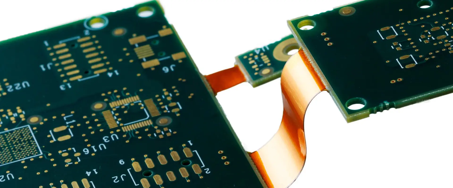
In today’s rapidly evolving electronics industry, the printed circuit board (PCB) serves as the backbone of virtually every electronic device. Whether you’re designing a smartphone, medical device, or industrial control system, selecting the appropriate PCB type can significantly impact your product’s performance, reliability, and cost-effectiveness. The two primary PCB categories—rigid and flexible—each offer distinct advantages and limitations that must be carefully considered during the design phase.
This comprehensive guide explores the fundamental differences between rigid and flexible PCBs, their unique characteristics, applications, and the key factors to consider when determining which type best suits your specific project requirements.
A rigid PCB is the traditional, non-bendable circuit board that has been the industry standard for decades. These boards consist of a solid substrate material that maintains its shape under normal conditions and provides a stable platform for mounting electronic components.
The typical structure of a rigid PCB includes:
A rigid substrate base (commonly FR-4 epoxy glass)
Silkscreen for component identification and reference designators
Common Materials
The most widely used material for rigid PCBs is FR-4 (Flame Retardant-4), a glass-reinforced epoxy laminate that offers excellent electrical insulation properties, mechanical strength, and relatively low cost. For specialized applications, other materials may be employed:
FR-1 or FR-2 (phenolic and paper laminates) for simple, low-cost applications
Ceramic substrates for high-frequency or high-temperature environments
Metal core PCBs (aluminum or copper) for enhanced thermal management
High-Tg FR-4 for improved thermal reliability
Typical Applications
Rigid PCBs dominate numerous markets due to their durability, ease of manufacturing, and cost-effectiveness. Common applications include:
Suitable for through-hole and surface mount components
Disadvantages of Rigid PCBs:
Cannot be bent or flexed
May require more space in compact devices
Limited design flexibility for complex 3D applications
Potentially heavier than flexible alternatives
May require additional interconnection methods
What is a Flexible PCB?
Definition and Structure
Flexible PCBs (also known as flex circuits) are thin, lightweight circuit boards designed to bend, fold, and flex during installation and operation. Unlike their rigid counterparts, flex PCBs can conform to three-dimensional shapes, making them ideal for applications with space constraints or dynamic movement requirements.
The primary substrate material for flexible PCBs is polyimide (such as DuPont’s Kapton®), which offers excellent electrical properties, temperature resistance, and mechanical flexibility. Other materials in flex PCB construction include:
Adhesives for bonding copper to the substrate
Coverlay materials (polyimide or polyester) for protection
Selective stiffeners (FR-4, polyimide, aluminum) for component mounting areas
Specialized surface finishes suitable for flexible applications
Common Applications
Flexible PCBs excel in applications where space constraints, weight reduction, or dynamic flexing are critical factors:
Medical devices (hearing aids, pacemakers, implantable devices)
Can be bent, folded, or flexed to fit tight spaces
Significantly reduced weight and thickness
Elimination of connectors and wiring harnesses
Better resistance to vibration and mechanical stress
Enhanced packaging capabilities for 3D applications
Improved thermal management in certain configurations
Disadvantages of Flexible PCBs:
Higher manufacturing costs compared to rigid PCBs
More complex design rules and constraints
Limited component density in flexible areas
Specialized handling requirements during assembly
Potential flex fatigue in dynamic applications
Less standardized manufacturing processes
Key Differences Between Rigid and Flexible PCBs
Understanding the fundamental differences between rigid and flexible PCBs is essential for making informed design decisions. The following comparison highlights the most significant distinctions:
Material Composition and Physical Properties
Feature
Rigid PCB
Flexible PCB
Base Material
FR-4, ceramic, metal core
Polyimide, polyester
Thickness
1.5mm-3.0mm typical
0.1mm-0.2mm typical
Flexibility
None
High (can bend 90° or more)
Weight
Heavier
Significantly lighter
Thermal Expansion
Higher coefficient
Lower coefficient
Vibration Resistance
Lower
Higher
Design Flexibility and Constraints
Rigid PCBs conform to a two-dimensional plane, limiting their application in complex three-dimensional spaces. In contrast, flexible PCBs can be designed to fit virtually any three-dimensional shape, enabling innovative form factors and integration possibilities.
However, flex PCB designs must carefully consider bend radii, neutral axis positioning, copper trace orientation, and other mechanical factors that aren’t typically concerns with rigid designs.
Durability and Reliability
While rigid PCBs excel in applications requiring structural stability and component support, flexible PCBs often demonstrate superior durability in environments with vibration, shock, or thermal cycling. The lack of rigid interconnections and the ability to absorb mechanical stress contribute to the enhanced reliability of flex circuits in dynamic applications.
Cost and Manufacturing Complexity
Rigid PCB manufacturing is a mature, highly standardized process with lower material costs and fewer specialized requirements. Flexible PCB production involves more specialized materials, tighter process controls, and often more complex handling procedures, resulting in higher overall costs—particularly for low-volume production.
Factor
Rigid PCB
Flexible PCB
Material Cost
Lower
Higher
Tooling Cost
Lower
Higher
Process Complexity
Standard
Specialized
Minimum Feature Size
Larger
Smaller
Production Time
Shorter
Longer
Volume Price Break
Reaches lower costs at lower volumes
May require higher volumes for cost efficiency
Rigid-Flex PCBs: A Hybrid Solution
Combining the Best of Both Worlds
Rigid-flex PCBs represent a hybrid approach that integrates rigid board sections with flexible interconnections in a single, unified structure. This technology combines the stability and component-mounting capabilities of rigid PCBs with the space-saving and dynamic benefits of flexible circuits.
The construction typically involves:
Rigid sections built with FR-4 or similar materials
Flexible sections using polyimide
Specialized lamination processes to bond the different materials
Careful layer stack-up planning to manage stress points
Benefits of the Hybrid Approach
Rigid-flex technology offers numerous advantages in complex electronic applications:
Elimination of connectors between board sections
Enhanced reliability through reduced interconnection points
Optimized space utilization in three-dimensional environments
Improved signal integrity with shorter, controlled-impedance paths
Simplified assembly processes
Reduced overall system weight
Use Cases and Applications
Though typically more expensive than either rigid or fully flexible options, rigid-flex PCBs excel in high-reliability applications where failure is not an option:
Selecting the optimal PCB technology requires careful consideration of various project-specific factors:
Mechanical Requirements
Space constraints: If your application has severe space limitations or requires conforming to a non-planar surface, flexible or rigid-flex PCBs may be necessary.
Dynamic movement: Applications requiring repeated flexing during operation (like folding displays or moving parts) typically demand flexible circuits.
Structural support: If the PCB provides structural integrity to the device, rigid boards usually offer superior performance.
Electrical Performance Needs
Signal integrity: High-frequency applications may benefit from the controlled impedance capabilities of either rigid or flexible designs.
Power handling: Heavy copper requirements for high-current applications are generally easier to implement on rigid PCBs.
Thermal management: Heat dissipation requirements may dictate PCB type selection, with metal-core rigid PCBs offering advantages for high-power components.
Environmental Considerations
Temperature extremes: Both rigid and flexible PCBs can be designed for high-temperature environments, but material selection becomes critical.
Vibration and shock: Flexible circuits generally provide superior resistance to mechanical stress.
Chemical exposure: Material compatibility with environmental conditions must be evaluated.
Budget and Timeline Constraints
Production volume: Higher volumes can justify the increased tooling costs associated with flexible PCBs.
Development budget: Rigid PCB prototyping is typically more cost-effective for initial design validation.
Time-to-market: Rigid PCB manufacturing generally has shorter lead times and more widely available fabrication services.
Design and Manufacturing Considerations
Design Rules and Requirements
Designing for rigid versus flexible PCBs involves different considerations and constraints:
Limited number of manufacturers with full capabilities
Special tooling often required for complex designs
Cost Implications
Cost factors vary significantly between PCB types:
Material costs:Flexible circuit materials typically cost 3-5 times more than standard FR-4.
Engineering time: Flexible and rigid-flex designs often require more design hours.
Tooling costs: Flexible PCB tooling is generally more specialized and expensive.
Production runs: Larger volume production can offset the higher initial costs of flexible circuits.
Assembly costs: Rigid PCBs typically have lower assembly costs due to standardized processes.
Common Mistakes to Avoid
Application Mismatch
One of the most expensive errors is selecting an inappropriate PCB type for the application:
Using flexible PCBs where rigid boards would be more cost-effective
Attempting to implement a rigid design in applications requiring flexibility
Over-engineering with rigid-flex where simpler solutions would suffice
Design Oversights
Common design pitfalls include:
Ignoring bend radius limitations in flexible circuits
Failing to account for flex fatigue in dynamic applications
Improper component placement relative to bend areas
Inadequate strain relief at transition points in rigid-flex designs
Incorrect stack-up planning resulting in neutral axis misalignment
Manufacturing Preparation Errors
Preparing manufacturing data incorrectly can lead to costly mistakes:
Insufficient documentation of bend requirements
Missing bend line indicators on fabrication drawings
Inadequate specification of material requirements
Unclear layer stack-up definitions for rigid-flex designs
Improper panelization for efficient production
Conclusion
The choice between rigid, flexible, or rigid-flex PCB technology is pivotal to the success of any electronic product. Each type offers distinct advantages that must be carefully weighed against project requirements, constraints, and objectives.
Rigid PCBs continue to dominate the market due to their cost-effectiveness, ease of manufacturing, and suitability for a wide range of applications. Flexible PCBs provide unique solutions for space-constrained, lightweight, or dynamic applications where traditional rigid boards fall short. Rigid-flex technology bridges the gap between these options, offering enhanced reliability for mission-critical systems where failure is not an option.
Ultimately, the most successful PCB selection process involves thorough analysis of mechanical, electrical, environmental, and economic factors, coupled with early collaboration between design, manufacturing, and assembly teams. By understanding the fundamental differences between these PCB types and their respective strengths and limitations, designers can make informed decisions that optimize their products for performance, reliability, and cost-effectiveness.
FAQs
What is the fundamental difference between a rigid and flexible PCB?
The primary difference lies in the base material and physical properties: rigid PCBs use stiff substrates like FR-4 that maintain their shape, while flexible PCBs use thin, bendable materials like polyimide that can conform to three-dimensional shapes and withstand dynamic flexing.
Is a flexible PCB more expensive than a rigid one?
Yes, flexible PCBs typically cost 30-50% more than comparable rigid PCBs due to more expensive raw materials, specialized manufacturing processes, and more complex handling requirements. However, they may reduce overall system costs by eliminating connectors, reducing assembly steps, and enabling more compact designs.
When should I use a rigid-flex PCB?
Rigid-flex PCBs are ideal for applications requiring high reliability, reduced weight, and complex three-dimensional packaging where traditional interconnection methods would create reliability issues or take up too much space. Common applications include aerospace, medical devices, and high-end consumer electronics.
Can flexible PCBs be used in high-power applications?
While flexible PCBs have limitations regarding thermal dissipation compared to metal-core rigid PCBs, they can be designed for moderate power applications by incorporating techniques such as wider traces, additional copper weight, strategic use of stiffeners, and thermal management features. For very high-power applications, rigid or metal-core PCBs typically remain the preferred choice.
How does the design process differ between rigid and flexible PCBs?
Flexible PCB design requires additional considerations including bend radius limitations, neutral axis calculations, trace routing relative to bend lines, specialized material stack-ups, and dynamic stress analysis. Designers must also specify coverlay openings rather than traditional solder mask and may need to incorporate stiffeners for component mounting areas.