Top 21 Largest EMS companies in World

EMS Manufacturing Companies

Electronic manufacturing services are a bridge between consumers and manufacturers. The operations of such firms are mainly integral to the medical sector. All the EMS firms are not constant with their services. 

Different EMS varies in the professional services they provide. Thus, these are important to stabilize consumer demand by increasing the supply. As time passes, the EMS will be dominating major sectors in the near future, as per the reports. 

There are several EMS firms functioning in the market. In this post, we are going to review a few of them for you! Letโ€™s get started without further ado!

What is EMS Manufacturing?

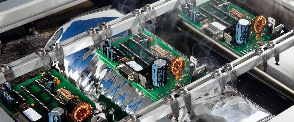
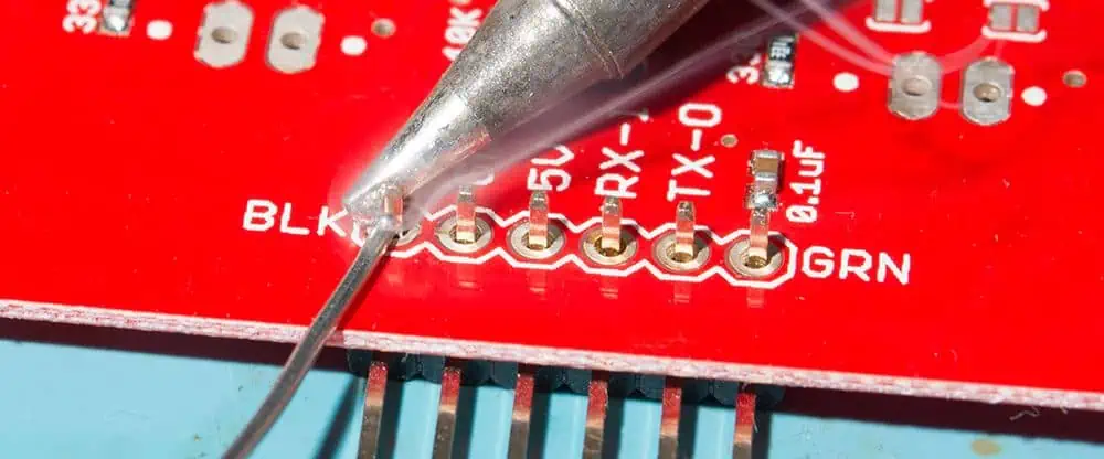
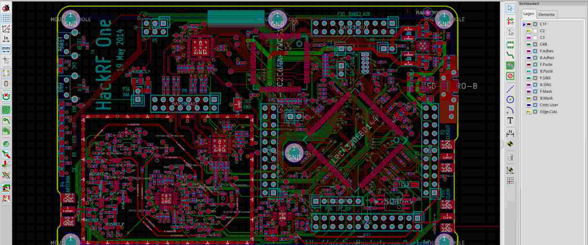
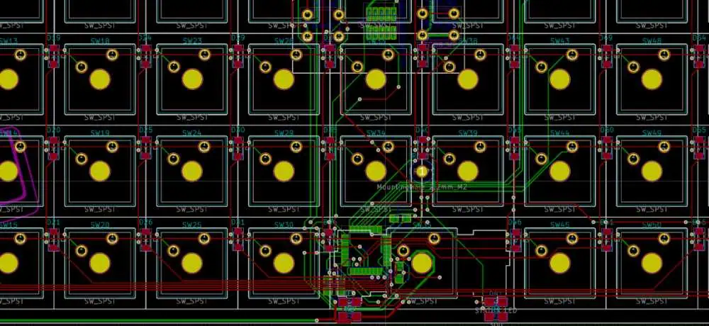
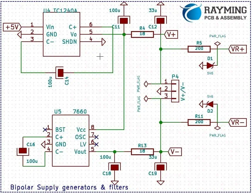
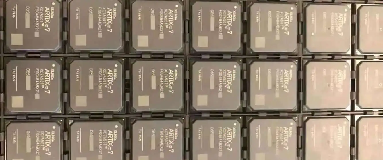
EMS production means designing and analyzing the PCBs and assembling their parts. The core responsibility of an EMS firm is to stabilize these tasks as much as possible. EMS manufacturing is not smooth sailing at all.

 Different factors like equipment and guidelines make EMS manufacturing a critical process in the PCB industry. Due to this reason, a specialized and experienced EMS producer is necessary to make all this possible. 

You already know why PCBs are crucial for different consumer electronics. EMS firms carefully produce their products for OEMS and collaborate with them. All the companies that design and check PCBs are EMS manufacturers.ย 

Factors to Consider while Choosing the Best EMS Company

EMS-Electronic-Manufacturing-Services-In-Malaysia

Now itโ€™s time to have a look at some factors that make the EMS producers stand out from the rest:

ยท Extensive experience & history

Every seasoned EMS firm boasts a vast experience in this industry. The company has a broad portfolio and has a big client base as well. It helps them serve new clients and sustain prolonged working relationships in the sector. A company with only 1-2 years of experience might not perform as per your expectations. So always rely on an old player to not compromise your interests at all. 

ยท Adherence to regulations & certifications

There is an important framework of guidelines for every industry. Similarly, a suitable EMS firm is one that strictly follows industry regulations. One easy way to find out is to look for their certifications and awards. It will help you analyze their performance in the past so that you can invest in a suitable EMS producer.

ยท Manufacturing capacity

A reliable EMS producer is one that offers impressive production capacity. It means they can deal with any possible complication and never compromise on the manufacturing rhythm at all. In this case, you can rely on an EMS firm that works like this. 

They would always work with eligible staff, precise products, effortless PCB assemblies, and flawless PCB designs. 

ยท Product testing

It is obvious that EMS providers manufacture PCBs so that they can function with electronic devices. It helps in the regulation of the electronics sector and stabilizes the workflow. Some consumer electronics can also face adverse environmental conditions. Due to this, it is important for EMS providers to test and completely analyze their products for their clients. 

ยท Communication channels

EMS companies must be active with their communication channels. From their website to social media platforms, the company must be able to address your queries. The customer support of a good EMS provider can reduce a lot of hustle for you at the same time. 

Important announcements, discount offers, changes, and other technical modifications among the products should be the top priorities of EMS providers. 

ยท Product introduction processes

No EMS can work actively without following a process for production. As technology always keeps changing. A first-rate EMS firm is one that modifies its working process as per the recent trends and client needs. A basic process that most EMS firms follow includes:

  • Brainstorming a perfect design for PCBs
  • Develop a prototype for this design
  • Test and analyze the final product
  • Produce bulk products if needed

Top Biggest EMS Manufacturing Companies in World

FULL PCB MANUFACTURING Quote

Below are some exceptional EMS providers that have been contributing to the industry for many years:

1.ย Foxconn โ€“ $193.72bn

They are another EMS firm that offers remarkable PCB services. They have been able to generate impressive revenue because of their unmatched expertise. They have deep roots in the medical sector, where they offer their products and services.

 The companyโ€™s products are helpful for integrating monitoring equipment, scanners, and more. They work to make the functioning of laboratory gear effortless. Devices for identifying cancer also include their products.

2. Wistron โ€“ $31.37bn

Wistron is another renowned EMS provider in this sector. The company operates in Taiwan. The company has many competitors, but Apple is its main business rival in the sector. However, the company deeply focuses on supporting the medical sector through its products. 

Their products are beneficial for use in medical equipment to ensure accurate results and precise performance in the longer run. 

3. Jabil โ€“ $27.27bn

The company is functional in Florida. However, it has deep roots in several other countries. They boast an impressive workforce of hundreds of employees in different regions. They specialize in designing electronics and prototyping. 

Their products have prime applications in the fields of automation and consumer electronics. They have been offering their solutions for electronics for many years as well. 

4. Flex โ€“ $24.12bn

They are a Singaporean EMS provider. It is another considerable EMS firm that specializes in PCB-relevant services. The company has a vast experience in this industry and knows how to deliver the best possible results.

 They can work with clients coming from the automotive industry to develop systems for the communications industry. Not only this, their products go well with medical equipment and provide precise results. 

 They also collaborated with Pillips in 2019 to increase the production of ventilators to save the lives of as many patients as possible during those hard times. 

5. BYD Electronics โ€“ $10.59bn

BYD Electronics is a Chinese EMS provider. The company made its greatest contribution of all time in producing Covid masks for the people. It generated itself an impressive amount of revenue during this pursuit. 

They can literally help you build your dream by offering expert services in technical aspects without compromising the quality at all. 

6. USI โ€“ $7.45bn

They are Universal Scientific Industrial. A leading EMS firm that has been successful in generating a large amount of revenue over the years. They can easily collaborate with OEMS in different sectors, including the medical and automotive industries. The services offered by USI include:

  • Producing EMS parts for assemblies
  • Developing PCB designs
  • Conducting miniaturization for the automotive sector
  • Devising solutions for the medical sector for regulating sleep patterns and enhancing the hearing ability 

7. Sanmina โ€“ $6.96bn

Sanmina is famous since it deeply takes an interest in the medical sector to offer its services. They have successfully developed MRI systems, surgical bots, X-ray machines, scanners, and other small-to-big equipment for their clients.

 They hope to develop critical optical sensors in the future to rule out using extreme surgical procedures that will save time and energy. 

8. Kinpo Electronics โ€“ $4.49bn

They specialize in consumer electronics. Their portfolio is impressive as they have worked with several clients from different sectors. In the days of COVID, they were among those EMS providers who produced ventilators, covid masks, and disinfectors. 

Also, they manufactured smart mirror devices that would detect temperature changes to isolate people who needed covid testing. One extension of Kinpo Electronics deals with producing equipment for the medical sector that ensures body fitness and disease management and control.
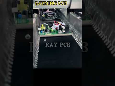
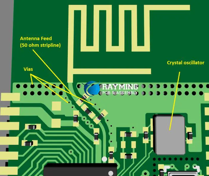
9.ย RayMing PCB & Assembly

The firm has been operational for many years. It is famous for its expert services in developing and designing consumer electronics. The company operates in China. It hosts an eligible workforce to deliver desired results to the clients.

 They use the latest equipment for prototyping, fabricating, and producing PCBs. You can rely on them for component sourcing of PCBs as well.

10. Plexus โ€“ $3.39bn

EMS FACTORY
EMS FACTORY

Plexus is important to talk about since it has been functioning for several years. It has a spectacular portfolio based on a huge clientele. They have successfully maintained their performance since the 1970s. They are an American EMS provider and offer expert services regarding PCBs and their assemblies. 

Their services are:

  • Supply chain regulation
  • Product designing (PCBs designs)
  • Production for OEMs
  • Manufacturing impeccable consumer electronics
  • Different natures of customer programs that are flexible

The company takes great pride in manufacturing compatible consumer electronics. They have set their own quality standards to ensure each of their products is flawless in nature. They only recruit eligible and adept engineers with an extensive technical background. 

11. Infineon Technologies

Experts mark Infineon as among the most reliable EMS providers. They have deep roots in the Malaysian consumer electronics sector. You can trust them with the durability of their products and the transparency of their services on all counts. 

Due to this reason, they are able to secure a strong position among their competitors. Their electronic solutions are error-free as well. They use the latest technologies to develop semiconductors for many technical applications in different domains. 

12. Keysight Technologies

They specialize in the field of electronics measurement. The company is integral for its remarkable services that cover this broad range. Letโ€™s have a look at their services to understand what are their areas of expertise!

  • They innovate solutions for modular devices
  • The company is best at developing software for technical domains
  • They can easily develop wireless gadgets 
  • Designing complex gadgets 
  • Building prototypes for electronics to ensure 100% efficient performance

13. Venture

The venture is another incredible EMS firm that is on our list. It deeply focuses on designing electronics and their production. Not only this, they are evolving former technologies to meet the future standards of the electronics domain. 

Another attribute of this firm is that they are experts in developing software as well. They rely on their ISO certifications to build trust among their customers. They never compromise the quality of their products. 

Also, Venture makes sure that its products undergo a complex process of quality checks before delivering them to the customers. They are flexible with the payments, and you can easily consult them to discuss your budget. 

They have active customer support that deals with the clientโ€™s queries and follow-ups to avoid any sort of problems. 

14. Pegatron

They have no parallel for their after-market facilities. It is a one-stop solution for EMS. They are famous for their impeccable PCB assemblies. Not only this, they handle flawless PCB designs for their clients as well. 

Whether the design is simple or complex, they deliver outstanding results. They are reliable producers of PCBs and electronics. They collaborate with different OEMs to deliver first-rate products to them. 

You won’t have problems regarding after-sale services as they make sure that everything is in place after you buy from them. Its products of Pegatron are useful in the electronics sector. Not only electronics they are reliable for computing.

15. First Solar

First Solar has been functional for about 15 years. They stand among the most reliable EMS providers of all time. The company has roots in global domains. They have an incredible workforce of engineers.

 They boast a convincing portfolio since they have a huge happy clientele. The stature of this company is hard to win over since it produces flawless photovoltaic solar panels. Not just solar panels, they are experts in their assemblies as well. 

Their solar systems work on slim modules to avoid any technical problems. Such a system eventually helps stabilize the economy and is cost-efficient at the same time. 

16. Ryder Industries, Xin Feng

They are another Chinese EMS provider. They specialize in impeccable turnkey solutions for the consumer electronics sector. The company has been active in producing electronics that never go wrong with functioning. 

You don’t have to worry about the efficiency and longevity of your electronics when buying from them. They set things right soon as the process starts and inspect their products through extreme quality check methods. 

It is better to have a look at the services offered by Ryder Industries to have a vivid review of them:

  • Developing firmware
  • Programming software solutions for the healthcare sector
  • Offers component sourcing 
  • PCB designing and prototyping

17. Fuji Electric

EMS Electronics Manufacturing Companies

They have been operational since the 1990s. There are some major areas that Fuji Electric specializes in. Due to this, you get an edge over your competitors while working with them. The three key types of major areas that they specialize in include:

  • Consumer electronics
  • Electrical solutions and energy regulatory devices
  • Retail systems

Following are the products and services that they offer:

  • Producing turbines
  • Developing power modules
  • Devising electronic solutions
  • Offers refrigeration services

18. Benchmark Electronics Inc

They are an EMS provider in Arizona. They work with the contract-based design of consumer electronics and production. Their integrated expertise has no parallel. There are several customers that have procured huge advantages from them. Their technology solutions are applicable to different domains as well. The applications of their products are:

  • Medical/healthcare sector
  • Aerospace and defense

It is important to know how this enterprise mainly differs from the rest of its eight factories active in different regions around the world. The services offered by this sole factory are:

  • Complete component inspection
  • Implementing precision technology for production
  • PCB design engineering
  • Impeccable computing
  • Critical data storage
  • Designing RF and high-speed products
  • Order completion 

19. Celestica Inc.

Celestica is another famous EMS firm. However, it operates in Canada. The company has offices in other regions around the globe. Its major clientele comprises Asian countries. They emphasize evolving consumer electronics through their expertise.

 Their engineers are adept at understanding the demand of their clients and performing with excellence. The products of Celestica are crucial for defense and aerospace applications. They also ensure the complete satisfaction of their clients by all means possible.

 You can also ask for supply chain services, as they are happy to help you with that as well. They never fail to impress with the after-sales services in case of any mishap or emergency. You can reach out to them through active customer support. 

20. EE Technologies

It is another American EMS provider. They operate in Nevada. They have a huge base of OEMs that they have worked with. Their expertise includes designing and producing futuristic electronics for their customers. 

These electronics never fail in their performance and promise efficiency on all accounts. No one can beat them with their style of PCB assemblies. They make this process easier by just helping you out with the problems.

 So that you can use these PCBs in complex devices later, all this is possible because they are well-familiar with using remarkable technologies to develop products of the future. 

21. Shenzhen Kaifa Technology

They are among the top Asian EMS providers. They have impressive rankings given by different technical institutes of the world. It helps them win the trust of their customers as well. It is a turnkey EMS firm that never disappoints with the end product. 

They work to develop useful PCBs that can increase the life length of electronics and medical equipment. Thus, this is why many OEMs from different domains are happy to work with them on and off. 

Not only this, consider them for procurement management and logistics control services in case you need them.ย 

Advantages and Disadvantages of Choosing EMS Company

through-hole assembly process

Just like everything has its pros and cons, EMS firms have some downsides and upsides that you need to keep in mind. It will help you in decision-making and will save you from possible complications as well. 

Advantages:

  1. Expertise: One benefit of hiring an EMS firm is that they will handle technical aspects like production, design, and inspection of your desired products. 
  2. Flexibility: EMS providers are flexible with their services and can devise ways to help you with your requirements that alleviate a lot of hustle and saves time. 
  3. Cost-effective: Their services are mostly cost-efficient, which means you don’t have to invest extra money in redundant services. Just consult them for a pricing package, and they will let you know about offered expertise based on the chosen package. 
  4. Time-to-market: EMS firms are crucial to increase the turnaround time, which eventually stabilizes the time-to-market. In case you are in a hurry, just outsource all the tasks to an EMS provider, and they will handle the rest for you.
  5. Supply chain management: EMS providers will source the production materials and ship them to their clients on their own. It means you don’t have to worry about the shipping hustle and material sourcing at all since it’s one of the main duties of an EMS provider. 

Disadvantages:

  1. Loss of control: EMS firms can slightly miss out on quality inspection, which can lead to faulty product designs. It usually happens when they are dealing with bulk production.
  2. Communication: You have to be able to actively respond to the EMS provider to ensure they understand your requirements and needs. Sometimes the clients don’t respond in time which can complicate the process on the EMS providerโ€™s side. 
  3. Dependency: If you always rely on such agencies, it can compromise your business values and can tarnish your reputation in the market with time. 
  4. Intellectual property risks: When hiring an EMS provider, it cannot guarantee to protect your substantial data, designs, and ideas. It means you are at risk of facing data theft since not all EMS firms are good at encrypting your data. 
  5. Price competition: There is no doubt that EMS providers are affordable to hire. However, sometimes illegitimate EMS firms can compromise on the quality of your products. As they will use cheap materials, it will create a negative impact on the final product later. 

Conclusion

EMS firms are significant in regulating the PCB sector. Their purpose is to transform the laborious part of the process into an easy one by offering their services. However, you need to make sure that your preferred EMS provider meets all the quality standards. 

You can now evaluate different EMS firms on the basis of some factors. It will help you choose the perfect fit for you every time. Keep in mind there are some definite cons to hiring an EMS provider. Make sure you don’t fall prey to an imposter EMS firm! 

Wave Soldering: A Comprehensive Guide to Process, Benefits, and Considerations

wave soldering temperature

1. What is Wave Soldering?

Wave soldering is an automated bulk soldering process used extensively in the electronics manufacturing industry. This efficient method is primarily employed for soldering electronic components to printed circuit boards (PCBs) on a large scale. The process derives its name from the wave-like formation of molten solder that the PCBs pass through during the soldering operation.

In wave soldering, a PCB with components already placed on it is passed over a standing wave of molten solder. This wave makes contact with the underside of the board, soldering all the components in one swift, continuous motion. The process is particularly effective for through-hole components but can also be used for certain surface-mount devices (SMDs) when properly configured.

Key Components of a Wave Soldering System

  1. Flux Application: A unit that applies flux to the bottom of the PCB
  2. Preheating Zone: An area where the PCB is heated to prepare it for soldering
  3. Solder Wave: The core of the system, where molten solder forms a wave
  4. Cooling Zone: Where the soldered board cools down and solidifies

Wave soldering has become an indispensable part of modern electronics manufacturing due to its speed, consistency, and ability to handle high-volume production efficiently.

YouTube video

2. How Wave Soldering Began

The evolution of wave soldering is a fascinating journey that spans several decades, marked by continuous improvements in efficiency and quality. Let’s explore the three main stages that led to the development of modern wave soldering technology.

First Stage: Dip Soldering

The precursor to wave soldering was a method known as dip soldering, which emerged in the early days of electronics manufacturing.

  • Process: PCBs were manually dipped into a bath of molten solder.
  • Advantages: Simple and effective for small-scale production.
  • Limitations:
    • Labor-intensive and time-consuming
    • Inconsistent results due to manual operation
    • Risk of thermal shock to components

While dip soldering was a step forward from individual hand soldering, it quickly became apparent that a more efficient method was needed as electronics production scaled up.

Second Stage: Drag Soldering

As the demand for electronic products grew, manufacturers sought ways to automate the soldering process, leading to the development of drag soldering.

  • Process: PCBs were dragged across the surface of a solder bath.
  • Improvements over dip soldering:
    • Increased automation
    • Higher throughput
    • More consistent results
  • Limitations:
    • Uneven solder application
    • Potential for solder bridges
    • Still relatively slow for high-volume production

Drag soldering represented a significant improvement in efficiency, but it still had limitations that needed to be addressed for large-scale manufacturing.

Third Stage: Wave Soldering

The breakthrough came with the invention of wave soldering in the 1950s, credited to the British company Fry’s Metals Ltd.

  • Key Innovation: Creation of a standing wave of molten solder
  • Process Improvements:
    • Continuous, automated soldering
    • Consistent solder application across the entire PCB
    • Significantly higher throughput
    • Better control over solder temperature and wave characteristics

Wave soldering quickly became the industry standard for high-volume PCB assembly, particularly for through-hole components. Its efficiency and consistency made it possible to meet the growing demand for electronic products in the latter half of the 20th century.

Modern Developments

Since its inception, wave soldering has continued to evolve:

  • Dual Wave Systems: Combining a turbulent and a laminar wave for better solder penetration and finish
  • Lead-Free Solder Compatibility: Adaptations to work with higher-temperature, lead-free solders
  • Integrated Flux and Preheat Systems: Improved process control and efficiency
  • Computer-Controlled Systems: Enhanced precision and repeatability

Today, wave soldering remains a crucial process in electronics manufacturing, coexisting with newer technologies like reflow soldering for surface-mount components.

3. What are the Advantages of Wave Soldering?

Wave soldering offers numerous benefits that have contributed to its enduring popularity in the electronics manufacturing industry. Let’s explore these advantages in detail:

1. High-Volume Production Capability

  • Throughput: Can process hundreds of PCBs per hour
  • Consistency: Maintains quality across large production runs
  • Cost-Effective: Lower per-unit cost for high-volume manufacturing

2. Excellent for Through-Hole Components

  • Reliable Connections: Ensures complete filling of plated through-holes
  • Versatility: Can handle a wide range of through-hole component types

3. Uniform Solder Application

  • Even Coverage: Consistent solder thickness across the board
  • Reduced Defects: Minimizes issues like insufficient solder or solder bridges

4. Efficient Use of Materials

  • Precise Solder Application: Minimizes waste compared to manual methods
  • Flux Control: Automated flux application ensures optimal usage

5. Process Control and Repeatability

  • Temperature Management: Precise control over solder temperature
  • Wave Characteristics: Adjustable wave height and speed for different PCB types
  • Consistent Quality: Reproducible results across production runs

6. Compatibility with Mixed Technology

  • Adaptability: Can be used for certain surface-mount components alongside through-hole
  • Flexibility: Useful for boards that combine different component types

7. Reduced Labor Costs

  • Automation: Minimizes the need for manual soldering
  • Skill Requirements: Less reliance on highly skilled operators

8. Speed and Efficiency

  • Quick Processing: Entire boards soldered in seconds
  • Continuous Operation: Can run for extended periods with minimal downtime

9. Improved Thermal Management

  • Controlled Heating: Preheating stages reduce thermal shock to components
  • Even Heat Distribution: Uniform heating across the board

10. Quality and Reliability

  • Strong Joints: Creates reliable solder connections
  • Reduced Human Error: Minimizes defects associated with manual soldering

These advantages have made wave soldering an indispensable process in electronics manufacturing, particularly for high-volume production of PCBs with through-hole components.

Read more about:

4. What is the Wave Soldering Process?

YouTube video

The wave soldering process is a sophisticated, multi-stage operation designed to efficiently and consistently solder components to printed circuit boards. Let’s break down each stage of this process in detail:

1. Flux Application

  • Purpose: Prepare the board and component leads for soldering
  • Process:
    • PCB passes over a foam fluxer or spray fluxer
    • Flux is applied to the bottom of the board
  • Functions of Flux:
    • Removes oxides from metal surfaces
    • Improves wetting of solder
    • Prevents re-oxidation during soldering

2. Preheating

  • Purpose: Gradually raise the temperature of the PCB and components
  • Process:
    • Board passes through a series of heating elements (infrared or convection)
    • Temperature typically raised to about 100ยฐC (212ยฐF)
  • Benefits:
    • Activates the flux
    • Reduces thermal shock
    • Evaporates flux solvents
    • Minimizes component stress

3. Solder Wave Contact

  • Purpose: Apply molten solder to the PCB
  • Process:
    • PCB passes over a wave of molten solder
    • Solder temperature typically 240-250ยฐC (464-482ยฐF) for lead-free solder
  • Wave Characteristics:
    • Laminar Flow: Smooth, even wave for consistent coverage
    • Turbulent Flow: Used in dual-wave systems for better penetration
  • Contact Time: Usually 2-4 seconds

4. Cooling

  • Purpose: Allow solder joints to solidify
  • Process:
    • Natural air cooling or forced air cooling
    • Temperature brought down to below solder solidification point
  • Importance:
    • Prevents component movement during solidification
    • Ensures strong, reliable solder joints

5. Cleaning (Optional)

  • Purpose: Remove flux residues and any contaminants
  • Process:
  • Considerations:
    • Environmental regulations
    • Type of flux used (no-clean vs. water-soluble)

Key Parameters in Wave Soldering

  1. Conveyor Speed: Affects exposure time to each process stage
  2. Solder Temperature: Critical for proper wetting and joint formation
  3. Wave Height: Determines contact area with PCB
  4. Flux Density and Application: Affects soldering quality and cleanliness
  5. Preheat Temperature Profile: Crucial for proper flux activation and minimal thermal stress

Advanced Techniques

  • Dual Wave Soldering: Combines a turbulent and a laminar wave
    • Turbulent wave for better penetration of plated through-holes
    • Laminar wave for smooth finish and removing excess solder
  • Selective Wave Soldering: Uses a focused, miniature wave for specific areas of the PCB

Understanding and controlling each stage of the wave soldering process is crucial for achieving high-quality results in PCB assembly.

5. Wave Soldering Defects

While wave soldering is generally a reliable process, various defects can occur if the parameters are not properly controlled. Recognizing these defects is crucial for maintaining quality in PCB production. Here are some common wave soldering defects and their causes:

1. Solder Bridges

  • Description: Unwanted solder connections between adjacent pads or leads
  • Causes:
    • Excessive solder wave height
    • Improper board design (insufficient spacing)
    • Contamination on the PCB surface

2. Insufficient Solder

  • Description: Lack of solder on joints, resulting in poor connections
  • Causes:
    • Inadequate flux application
    • Low solder wave height
    • Excessive conveyor speed

3. Solder Balls

  • Description: Small spheres of solder scattered on the PCB
  • Causes:
    • Excessive flux application
    • Contamination on the board
    • Turbulent solder wave

4. Icicles or Peaks

  • Description: Pointed solder formations extending from joints
  • Causes:
    • Improper cooling rate
    • Board exiting wave at wrong angle
    • Excessive solder temperature

5. Tombstoning

  • Description: One end of a component lifts off the board
  • Causes:
    • Uneven heating of component terminations
    • Poor component placement
    • Unbalanced pad design

6. Pinholes

  • Description: Small holes in solder joints
  • Causes:
    • Outgassing during soldering
    • Contamination on pads or leads
    • Insufficient preheat

7. Cold or Disturbed Joints

  • Description: Dull, grainy appearance of solder joints
  • Causes:
    • Insufficient solder temperature
    • Board movement during cooling
    • Contamination on surfaces

8. Solder Skips

  • Description: Areas where solder has not wet the joint
  • Causes:
    • Insufficient flux
    • Oxidized surfaces
    • Contamination

9. Excess Solder

  • Description: Too much solder on joints, often forming a blob
  • Causes:
    • Excessive wave height
    • Slow conveyor speed
    • Poor pad design

10. Component Damage

  • Description: Physical or electrical damage to components
  • Causes:
    • Excessive preheat or wave temperature
    • Thermal shock
    • Mechanical stress during process

Preventing Wave Soldering Defects

To minimize these defects, consider the following:

  1. Process Control: Maintain consistent temperatures, conveyor speeds, and wave characteristics
  2. Design for Manufacturability: Ensure PCB layout is optimized for wave soldering
  3. Cleanliness: Keep boards and components free from contamination
  4. Proper Flux Selection and Application: Use appropriate flux and apply it evenly
  5. Regular Maintenance: Clean and maintain wave soldering equipment regularly
  6. Quality Inspection: Implement thorough inspection procedures to catch defects early

By understanding these common defects and their causes, manufacturers can take proactive steps to improve the quality and reliability of their wave soldering process.

6. How Placement Can Affect the Effectiveness of Wave Soldering

The placement of components on a PCB plays a crucial role in the effectiveness of wave soldering. Proper placement not only ensures good solder joints but also minimizes defects and improves overall production efficiency. Here are key considerations for component placement in wave soldering:

1. Orientation of Components

  • Parallel to Wave Direction:
    • Ideal for most components
    • Ensures even solder distribution
  • Perpendicular to Wave:
    • Can cause shadowing and insufficient solder
    • Sometimes necessary for large components

2. Component Density

  • Spacing Between Components:
    • Adequate spacing prevents solder bridges
    • Allows for proper heat distribution
  • Clustering:
    • Avoid tightly clustered components
    • Can lead to heat buildup and soldering issues

3. Component Size and Shape

  • Larger Components:
    • Place downstream in wave direction
    • Prevents shadowing of smaller components
  • Tall Components:
    • Can create solder shadows
    • May require special consideration in placement

4. Thermal Considerations

  • Heat-Sensitive Components:
    • Place away from preheating zones
    • Consider using thermal relief pads
  • High Thermal Mass Components:
    • May require extended preheat
    • Consider placement for optimal heat absorption

5. Lead Length and Clinching

  • Lead Length:
    • Consistent lead length improves soldering uniformity
    • Too long can cause solder bridges; too short may result in insufficient solder
  • Clinching:
    • Can improve stability during soldering
    • Affects solder flow and joint formation

6. Pad Design and Component Footprint

  • Pad Size and Shape:
    • Affects solder wicking and joint formation
    • Should match component leads for optimal results
  • Solder Thieves:
    • Can be used to prevent solder bridges
    • Placement critical for effectiveness

7. Wave Direction Considerations

  • Component Entry Angle:
    • Affects how solder flows around leads
    • Generally, components should enter the wave lead-first
  • Exit Strategy:
    • Smooth exit from wave prevents icicles and peaks

8. Special Components

  • Connectors and Sockets:
    • May require specific orientation
    • Consider potential for flux and solder entrapment
  • Surface Mount Components:
    • When used in wave soldering, require special attention to prevent tombstoning

9. Clearance from Board Edges

  • Edge Clearance:
    • Maintain adequate distance from board edges
    • Prevents excess solder accumulation and edge defects

10. Mask and Solder Resist Considerations

  • Solder Mask Design:
    • Proper design prevents solder bridges and ensures good wetting
    • Consider mask clearances around pads

Best Practices for Effective Placement

  1. Design for Manufacturing (DFM) Review: Conduct thorough DFM reviews to identify potential issues before production
  2. Simulation and Modeling: Use thermal and fluid flow simulations to optimize component placement
  3. Prototyping: Build and test prototypes to verify placement effectiveness
  4. Continuous Improvement: Regularly review and update placement guidelines based on production results
  5. Training: Ensure design and production teams are well-versed in wave soldering principles

By carefully considering component placement, manufacturers can significantly improve the effectiveness of their wave soldering process, leading to higher quality PCBs and more efficient production.

7. What is the Difference Between Hand Soldering and Wave Soldering?

PTH Soldering
PTH Soldering

Understanding the differences between hand soldering and wave soldering is crucial for choosing the right method for a given project or production scenario. Each technique has its own strengths and limitations

Hand Soldering

  1. Process:
    • Manual application of solder to individual joints using a soldering iron
    • Operator controls solder amount, heat application, and timing
  2. Advantages:
    • Flexibility for various component types and board layouts
    • Ideal for prototyping and small-scale production
    • Allows for easy rework and repairs
    • Low initial equipment cost
  3. Limitations:
    • Time-consuming for large volumes
    • Consistency depends on operator skill
    • Potential for human error
    • Less suitable for high-density boards

Wave Soldering

  1. Process:
    • Automated bulk soldering where boards pass over a wave of molten solder
    • Machine controls solder temperature, wave characteristics, and board speed
  2. Advantages:
    • High-speed production for large volumes
    • Consistent results across multiple boards
    • Efficient for through-hole components
    • Cost-effective for high-volume manufacturing
  3. Limitations:
    • High initial equipment cost
    • Less flexible for varied board designs
    • Primarily suited for through-hole components
    • Potential for defects in complex board layouts

Key Differences

  1. Speed and Volume:
    • Hand soldering is slower but more flexible
    • Wave soldering is faster and more suitable for high-volume production
  2. Consistency:
    • Wave soldering provides more consistent results across boards
    • Hand soldering quality varies with operator skill
  3. Component Compatibility:
    • Hand soldering works with almost any component type
    • Wave soldering is primarily for through-hole components, with limited SMD capability
  4. Cost Structure:
    • Hand soldering has lower upfront costs but higher labor costs
    • Wave soldering requires significant initial investment but lower per-unit costs at scale
  5. Skill Requirements:
    • Hand soldering requires skilled technicians
    • Wave soldering requires machine operators and process engineers
  6. Flexibility:
    • Hand soldering allows for easy adjustments and one-off changes
    • Wave soldering is less flexible but more efficient for standardized designs
  7. Quality Control:
    • Hand soldering relies on operator skill and individual inspection
    • Wave soldering allows for more automated quality control measures

Choosing between hand soldering and wave soldering depends on factors such as production volume, board complexity, component types, and available resources. Many manufacturers use a combination of both methods to optimize their production processes.

8. Wave Soldering Design Considerations

Effective wave soldering requires careful consideration of various design elements. Here are key factors to consider when designing PCBs for wave soldering:

1. Solder Pad Mask Opening

  • Purpose: Defines areas where solder should adhere
  • Considerations:
    • Adequate clearance around pads to prevent solder bridges
    • Proper size to ensure sufficient solder coverage
    • Consistent openings for uniform solder distribution

2. Surface Finish

  • Options: HASL, ENIG, OSP, Immersion Silver, Immersion Tin
  • Considerations:
    • Compatibility with wave soldering process
    • Shelf life and oxidation resistance
    • Impact on solderability and joint reliability

3. Tips for Component Placement and Orientation for Wave Soldering

  • Orientation:
    • Align components parallel to the wave direction when possible
    • Place larger components downstream to prevent shadowing
  • Spacing:
    • Maintain adequate spacing between components to prevent solder bridging
    • Consider thermal relief for high-mass components

4. Component Clearances

  • Vertical Clearance:
    • Ensure sufficient space between component bodies and the board
    • Typically 0.5mm to 1.5mm depending on component size
  • Horizontal Clearance:
    • Space components to allow proper solder flow
    • Minimum 0.5mm between adjacent component leads

5. Pad Shapes

  • Through-Hole Pads:
    • Tear-drop shape can improve solder filling
    • Elongated pads in wave direction can enhance solder wicking
  • SMD Pads:
    • When used, ensure proper size and shape for component stability

6. Solder Flux

  • Type Selection:
    • Choose between no-clean, water-soluble, or rosin-based flux
    • Consider cleaning requirements and environmental factors
  • Application Method:
    • Ensure even application across the board
    • Consider flux density and viscosity for optimal performance

7. How to Take a Wave Soldering Profile

Taking a wave soldering profile is crucial for process optimization. Here’s a step-by-step guide:

  1. Attach Thermocouples:
    • Place thermocouples on various points of the PCB
    • Include locations near sensitive components and high-mass areas
  2. Run Test Board:
    • Pass the instrumented board through the wave soldering machine
  3. Record Data:
    • Collect temperature data throughout the process
    • Note temperatures at key points: preheat, solder wave contact, and cooling
  4. Analyze Profile:
    • Ensure proper preheat slope and peak temperatures
    • Verify solder wave temperature and contact time
    • Check cooling rate for proper joint formation
  5. Adjust Parameters:
    • Modify conveyor speed, preheat settings, or wave characteristics as needed
    • Repeat process until optimal profile is achieved
  6. Document Results:
    • Record the final profile for future reference and process control

By carefully considering these design elements and properly profiling the wave soldering process, manufacturers can significantly improve the quality and reliability of their PCB assemblies.

9. Wave Soldering Machine and Temperature Profile

Understanding the wave soldering machine and its temperature profile is crucial for achieving optimal results in PCB assembly. Let’s delve into the key aspects of wave soldering equipment and the importance of temperature management.

Wave Soldering Machine Components

  1. Flux Application System:
    • Foam fluxer or spray fluxer
    • Applies flux evenly to the bottom of the PCB
  2. Preheating Zone:
    • Infrared or convection heaters
    • Gradually raises board temperature to activate flux and prepare for soldering
  3. Solder Wave System:
    • Solder pot with pump mechanism
    • Creates a standing wave of molten solder
  4. Conveyor System:
    • Moves PCBs through the machine at a controlled speed
    • Often adjustable for different board types
  5. Cooling Zone:
    • Forced air or natural cooling section
    • Allows solder joints to solidify properly
  6. Control Panel:
    • Manages temperature, conveyor speed, and wave characteristics
    • Often includes data logging and profile storage capabilities

Temperature Profile in Wave Soldering

The temperature profile in wave soldering is critical for ensuring quality solder joints and preventing component damage. A typical profile consists of several stages:

  1. Flux Activation:
    • Temperature: 80-100ยฐC (176-212ยฐF)
    • Purpose: Activates flux for oxide removal and improved wetting
  2. Preheat Ramp:
    • Temperature: 100-150ยฐC (212-302ยฐF)
    • Purpose: Gradually increases board temperature to prevent thermal shock
  3. Soak:
    • Temperature: 150-170ยฐC (302-338ยฐF)
    • Purpose: Equalizes temperature across the board, completes flux activation
  4. Solder Wave Contact:
    • Temperature: 240-260ยฐC (464-500ยฐF) for lead-free solder
    • Purpose: Applies molten solder to form joints
  5. Cooling:
    • Rapid initial cooling to below 180ยฐC (356ยฐF)
    • Gradual cooling to room temperature
    • Purpose: Ensures proper joint formation and prevents thermal stress

Optimizing the Temperature Profile

  1. Board-Specific Profiling:
    • Adjust profile based on board thickness, component density, and thermal mass
    • Use profiling equipment to measure actual board temperatures
  2. Preheat Optimization:
    • Ensure adequate preheat to activate flux and reduce thermal shock
    • Avoid excessive preheat that can damage components or evaporate flux
  3. Wave Temperature Control:
    • Maintain consistent solder wave temperature
    • Adjust for different solder alloys (e.g., lead-free requires higher temperatures)
  4. Cooling Rate Management:
    • Control cooling rate to prevent defects like icicles or disturbed joints
    • Consider forced cooling for high-mass boards
  5. Process Window Development:
    • Establish a process window that allows for minor variations while maintaining quality
    • Document optimal settings for different board types

Advanced Features in Modern Wave Soldering Machines

  1. Dual Wave Systems:
    • Combines turbulent and laminar waves for improved penetration and finish
  2. Nitrogen Inerting:
    • Reduces oxidation and improves wetting, especially for lead-free solders
  3. Automated Profiling Systems:
    • Real-time temperature monitoring and profile adjustment
  4. Selective Soldering Capability:
    • Allows for targeted soldering of specific areas on complex boards
  5. Integration with Industry 4.0:
    • Data collection and analysis for continuous process improvement

By understanding and optimizing the wave soldering machine and its temperature profile, manufacturers can achieve consistent, high-quality results in their PCB assembly processes. Regular maintenance, careful monitoring, and continuous improvement efforts are key to maximizing the effectiveness of wave soldering technology.

Conclusion

Wave soldering remains a cornerstone technology in electronics manufacturing, offering unparalleled efficiency for high-volume production of through-hole PCB assemblies. From its humble beginnings in dip soldering to the sophisticated, computer-controlled systems of today, wave soldering has evolved to meet the changing needs of the electronics industry.

Key takeaways from this comprehensive guide include:

  1. The importance of understanding the wave soldering process and its various stages
  2. The critical role of proper component placement and PCB design for successful wave soldering
  3. The need for careful temperature profile management to ensure quality and reliability
  4. The advantages of wave soldering in terms of speed, consistency, and cost-effectiveness for high-volume production
  5. The ongoing relevance of wave soldering even in the age of surface-mount technology

As the electronics industry continues to advance, wave soldering will undoubtedly continue to evolve, incorporating new technologies and techniques to meet the challenges of increasingly complex and miniaturized electronic devices. By staying informed about best practices and emerging trends in wave soldering, electronics manufacturers can ensure they continue to produce high-quality, reliable products efficiently and cost-effectively.

Navigating CVBGA: A Step-by-Step Guide

BGA Chip

BGA package refers to chip carrier technology or surface-mounted ICs and other such devices, such as microprocessors. However, the package BGA offers low resistance of thermal, low inductance, and higher pin count than other packages. This gives high-speed performance and greater interconnection pins than flat or dual-in-line packages.

Despite its amazing features, BGA also has disadvantages. The soldering balls do not flex as large and long leads. At the same time, the density of the package causes difficulty in inspection for damage and faults. Moreover, soldering devices for mass production can cost much.

Regardless of its disadvantages, the BGA package still refers to an ideal option for various applications. 

Overview of CVBGA

CVBGA stands for Very Thin Chip Array Ball Grid Array. It refers to a kind of IC or Integrated Circuit type. It is specially designed to give features that are compact and thinner than conventional CTBGA and BGA packages. This article gives you a detailed insight into the advantages and features of CVBGA package technology, along with its use cases and applications.

The IC package of CVBGA design is lightweight and ultra-think aspect. However, this feature makes it perfect for portable and wearable devices that need small structure aspects as compared to the CTBGA package. The package of CVBGA consists of copper traces, solder of all ball layers, and ceramic substrate over the bottom surface of a CVBGA package. Advanced techniques of manufacturing like chip thinning and wafer thinning help in achieving package thinness.

Features & Advantages Of CVBGA

BGA Rework Services

ยท Ultra-thin Form Factor

The ultra-thin factor of the CVBGA package is the primary and essential feature that attracts a large number of consumers. It has a thickness of 0.5mm or less. Moreover, they are specially designed in thinner form to choose for mini portable devices as small factors play a vital role in portable devices. Thus, making this technology an appropriate choice in applications like medical devices, wearables devices, and mobile devices where space acts as a premium factor.

ยท High Pin Count

Regardless of the small size of the CVBGA package, it supports higher PINs. This allows higher performance and complex circuits. This feature is especially critical for devices like mobile electronics. As they require higher pin count in connectivity chips and high-speed processors to make connections among the components. 

ยท High Thermal Performance

The high thermal conduction of the CVBGA package aids in dissipating the heat fastly and efficiently. However, this ensures that the ICs work well even under extreme workloads. This feature plays a vital role in devices like industrial equipment and automotive electronics. As these the ICof these devices have to work in strong conditions along with high temperatures.

ยท High Reliability

The reliable and robust features of CVBGA packaging ensure that the IC works efficiently and stably in harsh and extreme environmental conditions. Moreover, this feature tends manufacturers to use it for medical devices, defense and aerospace, and automotive electronics, as reliability is one of the main factors of these devices.

ยท Low Manufacturing Costs

The cost-effective feature of CVBGA enables it to be used for the mass production of electronic devices. Mass production plays an essential role in consumer electronic devices as the cost is one of the factors that determine the success and failure of a device.

Applications and Uses Of CVBGA

The technology of CVBGA offers various benefits along with several use cases. Because of its ultra-thin appearance, it is used in a wide range of applications and electronic devices. Some of the primary use cases and application of CVBGA packaging includes the following:

ยท Mobile Devices

Mobile devices like tablets and smartphones use CVBGA packaging in them. The higher pin count and ultra-thin structure of CVBGA packaging make it ideal for use in memory ICs, Connectivity chips, and mobile processors. Moreover, CVBGA packaging’s high thermal conduction feature ensures that all the devices work reliably and efficiently, even under greater workloads.

ยท Wearable Devices

Wearable devices like fitness trackers, medical monitoring equipment, and smartwatches require high reliability and compact size. However, the technology of CVBGA provides both features, which makes it an appropriate choice for use in wearable Integrated circuits. CVBGA offers low-cost manufacturing. Thus, making this technology cost-effective for the mass production of tiny, wearable devices.

ยท Automotive Electronics

The industry of automotive starts relying on the latest and most advanced electronic components for connectivity, performance, and safety measures. The high reliability and high thermal conduction of CVBGA packaging consider it ideal for operating automotive ICs that work in harsh and extreme environments. Additionally, the CVBGA technology’s higher pin count provides greater support to complex circuit boards for infotainment systems and ADAS.

ยท Aerospace And Defense

FULL PCB MANUFACTURING Quote

The defensive and aerospace industry needs electronic components with the ability to withstand harsh environments like shock, vibration, and high temperature. The robust design and Extreme thermal conduction of CVBGA technology make it a great choice for such devices. Moreover, CVBGA packaging with a higher pin count also provides great support to complex circuits for critical devices.

ยท Medical Devices

Medical equipment and devices need high precision and reliability, which makes CV BGA packaging an appropriate choice. However, the ultra-thin aspect of CVBGA technology permits the development of compact medical equipment. These devices include implantable medical gear. Moreover, the CVBGA packaging’s higher pin count also gives support to complex and difficult circuits, especially for medical equipment.

Conclusion 

CVBGA, or very thin CABGA, refers to a kind of Integrated Circuit package. It is specially designed in a lightweight and ultra-thin aspect. This makes it appropriate for wearable devices that need a small size factor. 

However, it offers various advantages and features, which include ultra-thin aspect, high thermal conduction, high reliability, higher pin count, and low cost of manufacturing. Mobile devices, automotive electronics, consumer electronics, medical devices, and wearables devices use the technology of the CVBGA package.

How to Make Schematic Diagram

KiCad schematic tutorial

The plan of any printed circuit board starts from its schematic layout. The schematic layout of the circuit board may be described as a utilitarian graph or circuit chart of the electronic circuit. Also, images are utilized for communicating with the components as well as the way in which theyโ€™re electrically associated.

What Does a PCB Schematic Diagram Mean?

A schematic diagram can be described as a circuit design of two dimensions that shows the connectivity and functionality between the two components. At times, we refer to it as a PCB schematic or Schematic.

Also, PCB designs can be described as three-dimensional layouts, which describe the locations of the components as soon as you discover that the circuit is working. Then, this PCB schematic is the initial part of the PCB design.

This can also be depicted as a pictorial representation, which is either on a computer or written, which makes use of symbols that agreed upon for describing the circuit connections. Also, it indicates those components, which would be utilized and the manner in which they will be connected. This schematic diagram must be readable by anyone.

What is PCB Schematic?

kicad-schematic

PCB schematic is a blueprint and a plan. Its major concern isnโ€™t where the location of these components will be. Rather, this schematic will lay out the way the printed circuit board will achieve connectivity and create an important aspect of your planning process.

Upon the completion of the blueprint, the design of the PCB follows. This design involves the physical representation or layout of your PCB schematic. It also includes the hole layout and copper track. This PCB design reveals the componentsโ€™ location coupled with their connection with copper.

The PCB design phase is the one committed to performance. The Engineers create the real components right on top of your PCB design. This allows the testing of the device if it functions or not. Also, we have mentioned earlier that the PCB schematic should be easy to understand by everyone, however one cannot readily understand the functionality just by taking a look at the printed circuit board prototype.

Immediately the two phases are completed and you are okay with the PCBโ€™s performance, then the PCB manufacturer can now ensure that the device is brought to life.

What are the Elements of the PCB Schematic Diagram?

Now you understand the differences between PCB design and PCB schematic. Itโ€™s time to consider the elements of the PCB schematic diagram. As mentioned earlier, all connections will be visible; however, there are some important things to consider.

  • To see all the connections clearly, they arenโ€™t created to scale; they might be close to each other n your PCB design
  • Some connections may cross, which will not happen when using the physical version
  • Also, some of the connections may be on the layoutโ€™s opposing sides with markings that indicate linkage between them
  • The blueprint of the PCB may be presented on a single page, double pages, or several pages. It can take as many pages as possible to completely depict everything necessary for inclusion into the design.

The final thing to consider is that schematics that are more complicated might be categorized by their function. This is done to ensure readability. Furthermore, the arrangement of the connections this way is something that wonโ€™t happen during the following stage and the schematics usually will not match up till the 3D modelโ€™s final design.

What are the Elements of a PCB Design?

This stage involves the movement from the written blueprints into a unique physical representation which is constructed making use of a ceramic or laminate material. Also, some applications that are more complicated need flexible PCBs where tight space becomes a concern.

Furthermore, the PCB design elements work with the blueprint which the process of the schematics has already laid out. However, as already mentioned, they look visually distinct. Regarding PCB designs, we are referring to a 3D model which includes the PCB as well as the design files. Also, they could be multiple or single layers, although most times they are usually made up of two layers. Some differences exist between the PCB design and PCB schematics.

  • All the components will be in the right position an right size
  • If the two connections should not be connected, then you must prevent any form of crossing between them on same level. You can achieve this by changing to a different layer or having a detour

Guidelines on How to Create Schematic Diagram

FULL PCB MANUFACTURING Quote

You need to understand how some elements are designed when creating a schematic diagram for a PCB. These are guidelines to help you with your schematic diagram.

Page size option

The majority of design software available provides separate page sizes. Therefore, the PCB designer needs to decide the page sizes to use according to the estimate of the PCB plan.

Page naming agreement

The schematic diagram comprises logical blocks which are separated in pages. You have to place pages alphabetically. In most cases, designers ignore the block charts and then go through the history aas this helps in saving time. However, the ย block charts are easier for some designers to understand.

Grid settings

The tool needs some reference, but it isnโ€™t a necessary requirement from PCB designers. Designers will be able to reference parts and connect correctly when there is a grid. PCB components must always be on the grid and enable the probing of network during the inspection.

Page title bar

You will find the page title bar in the schematic pageโ€™s footer. It includes specific details such as record number, size, date of update, name or function of circuit.

Comments

PCB designers have to include the important notes about the circuit board. Also, messages can be written in schematic drawing pages or standalone documents. Also, there are annotations on distinct pages for complex designs. Some of the comments include PCB layout guides and jumper states.

Revised history

Revision history makes record for any altercation in the PCB design. This document offers details about the names of reviewers and author, the review, and a description of the altercation. Also, the revision history is usually at the final page of the PCB schematic layout.

Block diagram

Block diagrams reveals different modules that are within the flag flow and the plan. Therefore, it helps reviewers to have a good understanding of the design.

Layered schematic diagram design

It is usually advised to have a layered structure of the circuit board stackup design has a wide range of modules. Therefore, the hierarchy circuit diagram reveals that there is a flow of flag from a module to another. You can select one of these modules to have a well-detailed view of the module.

Component reference

The component reference reveals the corresponding reference indicators and the names of the standard PCB components integrated in any PCB schematic diagram. You can assign indicators based on the IEEE standard. Also, you can name components by using certain reference flags. Make sure you use uppercase letters always.

Why is a PCB Schematic Diagram Important?

A PCB schematic diagram offers a visual representation of a circuit board. The PCB schematic graph is one of the important part of PCB design. One of the functions of a PCB schematic diagram is that it can define the connections between different electronic components. Specifying the connections between these components is a crucial step in the plan of a gadget.

Before this, PCB designers usually drew circuit charts on paper. However, they have started using apparatuses that streamline the preparation of the plan. Creating a schematic diagram can help in preventing PCB rework.

Reading the Circuit Board Schematics

To have good understanding of reading the circuit board schematics, you have to know the basics. This includes the network, reference indicators, output, and symbol.

Reference Mark

The reference designators usually want to recognize the names for every physical component. This proper use of the REFDES reveals the schematics for every user, the component type, as well as the amount of images for each component.

Also, the reference symbolโ€™s industry standard is made up of a specific letter code, which helps in demonstrating some component.

Network

In PCB and schematic parlance, the network is described as the electrical connection of a PCB wiring. Also, networks usually show as lines, which connect the component symbol pins onto the other networks or pins.

Component Symbol

 The schematicโ€™s symbol represents those parts that have to be joined or welded to the PCB during the assembly process. Then and now, they might speak to the circuit board structures like test focuses or through-holes. The symbo9ls of the component are mostly industry-standard drawings or shapes, which indicates the electrical component type that they are.

Output

Some important outputs are bills of material and netlists. This network list can be described as the major output of the circuit board layout software, which is useful to the designer for guiding the placement as well as wiring of all the circuits.

The BOM can be described as a database and spreadsheet, which matches each schematicโ€™s REFDES to a part number and physical component. The BOMโ€™s format is dependent on the part database and schematic as well as the required output type.

Symbols Used in PCB Schematic Diagram

In a PCB schematic diagram, there are several symbols included. Circuit symbols of electronic components represent the schematic of electronic components. These symbols vary in various regions or countries, the ANSI and IES established some common standards for representing these symbols. Also, these electronic circuit symbols reveal how to connect circuits.

Resistors

There are two ways to represent resistors. PCB designers must maintain the consistency of the symbols integrated. Ohm is the resistance unit and โ€œฮฉ,โ€ denotes this symbol.

Non-polarized and polarized capacitors

There are two different terminals in a capacitor. These are the negative and positive terminals. There could be an explosion if the polarity of a capacitor terminal is incorrect.

Transistors

These are three-dimensional semiconductor device that comprise a collector, an emitter, and a base. PCB designers need to refer to component data tables whenever foot print and pin layouts are mapped to schematic symbols. You need to input the unit of the valuable component when designing symbols. This is helpful for future reference.

Op-amp

The IEEE specified standards for creating op-amp symbols. Most PCB designers donโ€™t understand how to use CAD schematic tools and usually draw operational amplifier according to convenience. Therefore, it is advisable for all input pins to remain on the cleared out while output pins should be on the correct. You can place ground and power pins at the bottom and top, respectively.

Conversion of PCB to Schematic Diagram

Schematic Design in KiCAD

Draw the PCB for picture preparation

This is a step in reverse engineering which requires to take images using a dark background and capture both sides of the circuit board.

Upload images

You can upload the captured photo to a reverse engineering program. Ensure the image is cropped before uploading it. This will ensure the image shows on the circuit board only.

Construct the layout

After the image has been uploaded to the program, you need to design a 3D layout of the circuit. This layout reveals the arrangement of the electromagnetic field distribution of the system and the performance of the circuit.

Create a schematic

You need to obtain the schematic of the circuit board. When a PCB schematic is derived, all the components of each board and circuit can be seen. This drawing is in a two-dimensional CAD assembly drawing.

Conclusion

A PCB schematic diagram reveals the connections between components and wires in an electronic circuit. It is similar to a sketch for building a circuit board. This circuit diagram or wiring diagram provides all the necessary information about the functioning and performance of a circuit. A schematic diagram is an important part of a PCB design stage. Therefore, PCB designers must pay attention when drawing this diagram as it determines a lot of things during the design stage. The importance of a schematic diagram in PCB design canโ€™t be overemphasized.

What Is XCKU095-1FFVA1156I, Its Specifications, And Configuration

Xilinx Zynq fpga

FPGA has revolutionized the digital and electronic worlds. Not any circuitry is complete without these FPGAs. Previously integrated circuits were doing great, but nowadays, FPGAs are doing a wonderful job.  Thatโ€™s why you can easily customize m, configure, and re-configure them

XCKU095-1FFVA1156I is a high-performance FPGA. Xilinx, a leading provider of programmable logic devices, is the manufacturer. It belongs to the Kintex UltraScale+ family of FPGAs. This family is famous for their high bandwidth and low latency. Let’s dig deeper to learn about specifications.

Technical Specifications 

  • This particular FPGA features 1.3M logic cells. The basic building blocks of FPGA.
  • FPGA conation 864 DSP slices. It is a fairly good number of slices for any FPGA.
  • 4 MB RAM, making it one of the most powerful FPGAs on the market.
  • It also boasts a wide range of features and interfaces600 Gb/s transceiver bandwidth.
  • It has 2 x 100G Ethernet MACs.
  • DDR4 memory interfaces
  • High-performance 32-bit ARM Cortex-A53 application processing unit. It is enough for performing high-processing tasks.
  • All these features make XCKU095-1FFVA1156I a versatile and powerful FPGA that can be used in various applications.
  • It has 96 x 16.3Gbps GTY transceivers.
  • It has 60 x 12.5Gbps GTH transceivers. These transceivers are specialized hardware blocks. As a result, it can handle high-speed serial communication protocols,
  • Integrated DDR4 memory controllers for this FPGA
  • High-speed serial connectivity with Speed Grade for this FPGA is -1
  • The process Technology for this FPGA is 16nm FinFET+. It is the latest technology.
  • Clock Management Tiles for this FPGA is 10.
  • A number of inputs and put pins 523 for better connectivity and connection.

These features allow the XCKU095-1FFVA1156I to deliver high performance, low power consumption, and excellent integration capabilities. As a result, it is an excellent choice for a wide range of applications.

Alphanumeric Breakdown Of XCKU095

FULL PCB MANUFACTURING Quote

This is the Xilinx product family name and represents the specific device within that family. In this case, it’s the Kintex UltraScale family, and the specific device is the XCKU095.

  • 1FFVA1156I is the device speed and package type code. Here’s what each part of the code represents
  • One represents the speed grade of the device. In this case, it’s the -1 speed grade, which means it operates at a lower frequency than other speed grades within the same family. -2 is moderate speed
  • FFVA represents the package type and number of high-speed transceivers. The FFVA package has 1156 pins and supports 16 high-speed transceivers.
  • I represent the RoHS compliance status of the device, where I stand for RoHS-compliant. It means that it doesn’t conation any harmful material such as lead or anything else.
  • The XCKU095-1FFVA1156I configuration provides a high level of performance while still offering a high degree of flexibility. As a result, it is ideal for applications that require both high-performance computing and flexibility.

How To Choose the Right XCKU095-1FFVA1156I Configuration

Now that you understand the basics of FPGAs and the specifics of the XCKU095-1FFVA1156I configuration, let’s take a look at how to choose the right configuration for your needs.

Configuration of an FPGA refers to the process of loading a design or data file onto the FPGA. As a result, it can perform the desired function. Xilinx provides many configuration tools, that are why it is easy to configure the FPGA. You cannot configure every FPGA in the same manner. The following tips will help you to get the right configuration for your FPGA.

1. Determine Performance Requirements and Expectations.

The first step in choosing the right XCKU095-1FFVA1156I configuration is to determine your performance requirements. What tasks do you need your FPGA to perform? What are you expecting from your FPGA? How much processing power do you need for your work? This will help you determine which configuration is best suited for your needs. Every configuration can go with your needs. That’s why it is better to configure FPGA according to your need.

2. Look At The Specifications

 FPGA specifications also play an important role in configuration. Certain configuration doesn’t go with the specifications. In addition, specifications also don’t support some configurations. That’s why it is important to check the compatibility. For example if you neglect the specification later you will regret.

Once you have determined your performance requirements, it’s time to take a closer look at the specifications. As a result, you can check for the different XCKU095-1FFVA1156I configurations available. Look at factors such as the number of logic cells, the amount of memory, and the speed of the FPGA. Choose a configuration according to the specifications.

3. Consider Your Budget

Another important factor to consider when choosing the right XCKU095-1FFVA1156I configuration is your budget. Configurations are not free. You have to pay the price for them.

These configurations can vary in price. As a result, your budget may disturb. That’s why it is it’s important to consider how much you’re willing to spend. Keep in mind that a higher-performance configuration will generally come at a higher price. So it is always better to do extensive market research and take opinions from expert designers. You can choose the right configuration on a moderate budget without hitting the processing speed. It will take some time to do proper research to find the best confirmation. But in the end, you will, thanks.

 Above all, consider your requirements, your budget, and your configuration for your project.

 Final Thoughts

The XCKU095-1FFVA1156I is a highly capable FPGA. That’s why it meets the needs of demanding applications that require high performance, low power consumption, and high integration. It is built on a 16nm FinFET+ process technology. It is the latest technology, and it comes as a more power-efficient FPGA than previous generations of FPGA. As a result, you can expect more functionality from this FPGA.

The XCKU095-1FFVA1156I offers a wide range of features and capabilities, including high-speed serial connectivity and high performance. What else do you need from any FPGA? In addition, it supports a broad range of applications. So it is an ideal choice for all your next projects. You can choose it without hesitation.

Let’s Have a Detailed Overview of XC7Z030-1FBG484C Specifications

Xilinx Artix 7

 The XC7Z030-1FBG484C is a field-programmable gate array, aka FPGA device. That is manufactured by Xilinx. This FPGA belongs to the Zynq-7000 family. This family is known to integrate an FPGA with a dual-core ARM Cortex-A9 processor. The XC7Z030-1FBG484C is ideal for high-performance devices. That is suitable for various applications, including industrial control and video and image processing; let’s dig deeper to know more about this amazing FPGA.

Unique specifications make this FPGA stand out. Following are some unique features of this FPGA that make it ideal.

Device Architecture

 It is very important to know the device structure of any FPGA. It helps you to know the basic building blocks of FPGA. If you know the FPGA’s architecture properly, then you can use this particular FPGA in the best way.

  • The XC7Z030-1FBG484C device has great Architecture. It is based on the 28nm process’s latest technology. This FPGA features 535,000 logic cells. As you know, logic gates are so important in any FPGA. This FPGA has a good amount of logic cells.
  • It also has 1,060 DSP slices and 28.3 Mb of BRAM. Block Ram and DSP slices help to process data so fast.
  • Data storage is no longer an issue as this FPGA includes 6.6 Mb of Ultra RAM. Now two RAMs are working for storage and data processing. That’s why you can expect the best data storage.
  • A 10, 100, and 1000 Ethernet MAC and high-speed interfaces for PCIe, SATA, and USB are just icing on the cake.
  • That’s why this FPGA is unique among all other FPGAs.

Programmable Logic Makes This FPGA Easily Reconfigurable.

The XC7Z030-1FBG484C has a reconfigurable FPGA fabric that includes 535,000 logic cells. These logic cells can be configured to implement a wide range of digital circuits, including combinational and sequential Logic, memory elements, and specialized functions such as digital signal processing (DSP) and embedded processors.

High-Performance Processor

The XC7Z030-1FBG484C contains a dual-core ARM Cortex-A9 CPU. It has an amazing clock speed of one GHz. As a result, you can exact high data performance.ย 

Moreover, its central processing unit is highly versatile. That’s why you can utilize it for a multitude of high-performance software applications. You can easily perform 12 operating systems and other tasks. This FPGA also comes with a variety of peripherals and protocols. It all includes Ethernet and 

USB. UART interfaces are also one of them.

Exceptional Power Management

The XC7Z030-1FBG484C has a typical power consumption. It can consume 5.5 volts at a temperature of 85ยฐC. 85ยฐC is the ideal temperature for optimal working. However, the actual power consumption of the device can vary. It depends on factors such as the configuration of the FPGA fabric and the clock frequency. If you don’t maintain an ideal temperature, then it may consume more power. That’s why it is necessary to provide optimal temperature for optimal performance.

Enormous Memory For Data Storage And Faster Logic Functions

The XC7Z030-1FBG484C FPGA is a professional FPGA. XC7Z030-1FBG484C FPGA provides remarkable memory bandwidth. As a result, you have better functions, storage, and dispensation. It also includes a range of features that can enhance system performance, such as high-speed serial interfaces.  

Package And Pinouts

 When you come to packaging, it comes in convenience packaging. That’s why it is easy to handle and integrate.

The XC7Z030-1FBG484C comes in an FBG484 bundle. This bundle comprises a grand total of 484 pins. As a result, the device’s pinout has been refined for optimal high-speed signal routing. It also features a multitude of power and ground pins, as well as dedicated pins. As a result, these serve as high-speed interfaces for various devices. For example, it supports DDR3, SATA, and USB. That’s why it is easy to integrate this FPGA. Package and Pinouts play an important role when you need to do integration.

Supporting Development Tools

Development tools are important for configuration and other customizations in FPGAs. You can find different tools in the market, but Xilinx also provides a range of development tools. That’s why you can easily use it to design, implement, and debug FPGA-based systems. These tools are uncomplicated to use. For example, the Vivado Design Suite is an important and worthy tool for customization. It provides a comprehensive design environment for FPGA-based applications and systems. As a result, you can do your FPGA development functions straightforwardly. It has a range of other tools for developing functions. For example, IP cores and software development kits are ideal. Debuggers, for debugging purposes to, ensure smooth working.

Applications

FULL PCB MANUFACTURING Quote
  • The XC7Z030-1FBG484C is a versatile device that is present in a wide range of applications, including:
  • Industrial control and automation are easy with this FPGA. Now you have more control and precise control over automated systems. Automation is the future of every industry, especially the electronics and the digital industry.
  • Video and image processing is faster and result oriented. That’s why it also consumes less time.
  • Automotive and aerospace applications have a special place for this FPGA. These devices are delicate and space efficient, so this FPGA suits their needs best. Mostly compact and small devices are ideal for the aerospace field. This FPGA is ideal for all of them. So its future use may increase in the aerospace industry.
  • Embedded computing and high-performance computing devices have this FPGA. As a result, you can do logic functions easily.

 Wrapping Up

The XC7Z030-1FBG484C is an extraordinary FPGA. It has compiled an abundance of features in a solitary device. As a result, you get the highly intricate and best performance. Its Dual-core ARM Cortex-A9 processor is just the icing on the cake. Its power efficiency makes it an exceedingly attractive choice for engineers and designers. All designers looking for an efficient and energy-saving solution can go for it.

Overall, the XC7Z030-1FBG484C is a highly potent and flexible FPGA. It provides unparalleled performance and reliability. Therefore, if you are on the lookout for an exceptional  FPGA, the XC7Z030-1FBG484C is undoubtedly a must-go option. Further, you can compare it with other viable FPGAs in the market for better comparison.

What Is PCB Current Calculator, its Importance, And How To Use?

PCB Current Calculator

The PCB standard of IPC-2221 contains various requirements and specifications for the manufacture and design of circuit boards. Today, there are various web-based calculators that follow this standard. Apart from calculating the annular ring and impedance, it also focuses on the trace width, temperature rise, and trace current. Both standards, IPC-2152 and IPC-2221, include guidelines regarding designing the PCB for thermal tolerance. Both standards have a distinctly detailed debate over the applicability and usage of both standards. 

If you decide to choose the IPC-2221 standard, then donโ€™t be afraid. We have made a very simple and easy-to-use PCB calculator that helps to determine the limits of trace width in a given limit of heat. If you use Altium Designer, you can find these features in the Circuit Board Editor while working on the PCB routing.

Types Of PCB Current Calculators and Trace Width 

PCB-Trace-Width-Calculator

The trace width of PCB can be determined through various distinct calculators. All these PCB calculators follow the standard of the PCB industry. These PCB industry standards follow the guidelines for calculations. Both the IPC-2221 and IPC-2152 standards are widely used in commercial and industrial applications. 

1. IPC 2221 PCB Trace Width

The calculator IPC-2221 uses a graph and an equation to calculate the current of the PCB track. The formula stands for I=kฮ”TbAc.

In this formula, the Visible traces represent the K which has a value of 0.0048, and internal traces also represent the K which has a value of 0.024. ฮ”T represents the change in temperature in Celsius. The B value equals 0.44, and the C value equals 0.725. Whereas, A represents the area of cross-section.

The IPC-2221 calculator only uses a specific range of all values to calculate the PCB trace width. The range of current falls between 35 and 0 amperes, track width between 10.16 to 0 mm, the width of copper between 3 to 0.5 oz, and the rise in temperature between 100 to 10 oC. It does not give accurate results if the value changes from these specific ranges.

2. IPC 2152 PCB Trace Width

The Calculator IPC-2152 uses an advanced and recent standard type for the calculation. This gives a more precise and accurate calculation of Max capacity of trace current. It uses advanced technical methods. The formula of this calculator does not seem simple as compared to the calculator IPC-2221. To determine the unorganized area of the cross-section, it uses a universal graph.

However, this IPC-2152 calculator uses various types of parameters to create a number of modifiers. Therefore, the parameters include the thickness of the trace for passing, the distance between the tracks and copper planes, as well as the thermal conductivity of the PCB.

Whatโ€™s In IPC-2221 in Electronics Industry?

An IPC-2221 is a type of standard for the acceptance and qualification of PCBAs and PCBs. The standards demand some requirements and specifications to design a PCB, which ensure the manufacturability, reliability, and safety of a PCB. These standards come in generic standards. At the same time, you can specify a certain type of standard that applies to the PCB used in the whole series of 2220.

The IPC-2221 calculator uses the above formula to calculate the width of the PCB trace, which is needed to keep the level of temperature below a certain range. In simple words, you just have to enter the weight of the copper in the calculator. As a result, it gives you the value of trace width, which is required within the given temperature rise and current. 

Does the IPC-2221 calculator exist in an online system of CAD? Well, yes, the user of Altium Designer can avail of this tool in the tools of routing present in the window of PCB Editor. To analyze the trace width, just select the trace and then expand the information in the NEt Data area present in the Panel of Properties.

PCB Current Calculator: IPC-2221 Formula

FULL PCB MANUFACTURING Quote

The formulas mentioned above have some things to note to find which show precise and accurate results. 

  1. The formula is chart-based.
  2. The formula predicts that the PCB lies at STP in an open environment with air.
  3. The prototypes before using a trace of only thick PCBs and no extra copper planes to disperse heat.
  4. They treat multiple parallel closer traces as one bug trace to pass the current.
  5. If the thinness of the board falls below 30 mils, it recommends to derate it by 15% rather than 10%.
  6. Higher thermal capability substrates have distinct limits of trace and current width than a conventional laminate of epoxy-fiberglass.

This means that the IPC-2221 calculator does not give accurate results when it comes to modern PCBs. In simple words, the value of current capacity changes if you put an additional plane and copper around the trace, and it gives an underestimated value. On the other hand, it gets reversed with a minimum width of trace and gives an overestimated value. Remember these points, as it helps in calculating an accurate trace width.

Because of the nuisance of this standard with modern PCBs, designers and engineers were forced to create an advanced standard that gives higher efficiency, accuracy, and specificity. And then comes the IPC-2152 standard.

IPC-2221 Vs. IPC2152: Which is the Best to Use?

All online calculators have some limitations. The calculator IPC-2221 also falls in this category. Itโ€™s the fact that the IPC-2221 calculator gives an overestimated value of minimum trace width. Therefore, the standard IPC-2152 calculator expands the data to add numerous nomographs which determine the current limits, temperature rise, and trace width.

Currents a PCB Trace Carry and its Importance


The PCB trace current capacity limitation is one of the main problems which arise in various electronic projects. In many home projects, the value never exceeds the maximum limit, which seems better.

The calculator helps greatly in determining the current capacity of PCB trace yet gives a hard time in handling the charts. As the max PCB trace, the current capacity is linked with the operational temperature and width. 

Importance of Using the PCB Current Calculator Trace Width

The current calculator of PCB trace is an easy-to-use tool. It is divided into Output and Input sections which makes it easy to put data and obtain the results. The fields in this calculator include the following:

  1. The Internal and External trace location according to the substrate of PCB.
  2. The width of the trace represents the distance.
  3. The thickness of the trace represents the horizontal length of the PCB trace.
  4. The Max temperature rise represents the maximum value of a difference between the ambient temperature and PCB trace.

However, in advanced features:

  1. The surrounding temperature.
  2. The trace length from start to end.
  3. The Max PCB traces current capacity.
  4. The trace cross-sectional area.
  5. The temperature of trace while operation.
  6. The trace resistance at Max PCB traces current capacity.
  7. The drop of voltage for the max current and calculated resistance value.
  8. The dissipation of power at the max rate of current capacity.

Guidelines and Tips for Using the PCB Current Calculator 

The current that flows through the track and the specification of design determines the trace width of the PCB. However, it follows a specific rule. The minimum value of the traceroute ranges from 10 mm/A. This goes well for a 1.0 oz/ft2 thickness of copper.

The calculation of trace width is a complex process. That is why it requires some rules to understand for calculating the trace width of PCB. The circuit works well on max current with ambient temperature, the thickness of the trace, and the trace measurement unit. These values depict the input range of trace width.

When you add these values inside the calculator of trace width, it gives back some output values. This output value represents the PCB trace width. The datasheet shows all the figures of input. It does not work with guess figures. All PCB requires this information to calculate the trace width.

The calculator does not work well and gives no output if the input value is wrong. You may also need a magnifying glass so that you can see the exact values on the PCB.

Confirming the Efficient Trace Width with PCB Calculator 

ยท Standard Track Width

First, decide the track size for the PCB in your design. Too thin, narrow, and close tracks lead to short circuits. At the same time, too much spacing between the tracks must need some restriction on the track number. In such scenarios, incorporate extra plane layers in the PCB to make sure the routing of the PCB.

ยท Circuit Pad Shapes

The libraries of components typically possess PCB libraries for the schematic and footprint of different electrical components. Although, it depends on the process of PCB manufacturing. Therefore, you have to select the process of manufacturing before beginning the design process. This way, you can select the appropriate size of pads and later on incorporate it over the CAD system of PCB. 

ยท Track the Size of Lines

PCBs Possess a thin track of line which limits the carrying capacity of current. That is why we must consider the size of the trace for any route that carries a power current instead of lesser signal levels.

ยท Dimensions Of Hole & Pad

It’s important to decide on the pad and the hole dimension once you begin the design of the PCB. It may vary according to various situations. Sometimes, the ratio of pad-to-hole falls to 1:8. Sometimes, it measures when the pad is bigger than the hole. The manufacturers of PCBs have their own set of standards according to the usage of the application. The ratio gets more crucial as the size of the pads, and the hole decreases.

Factors to Think about When Developing PCB Trace Width 

The trace width of a PCB directly affects the functionality of a PCB in many ways. However, we have a few factors to take into account while determining the value of trace width.

ยท Signal Integrity & Electrical Performance

The majority of PCB digital routing possesses the default trace width value, yet some may need distinct sizes. For instance, the steady impedance net of traces needs the evaluation of trace width on the basis of the stack up of PCB layer consideration. 

In most cases, analog routing requires the PCB trace width according to the circuitry usage. Well, in some cases, one can also decrease the default width of traces in compact spaces. You only need to make sure that it will not extend the surface of the PCB. 

ยท PCB Fabrication

Wider traces fabricate easily on the PCB. The process of etching traces leaves a greater effect on the isolated and long traces. That is why make sure to create wider traces. For example, a trace of 20 mils has a greater current tolerance capacity than a trace of 3 mils. Moreover, the weight of the copper determines the width of the traces in a PCB.

ยท Power & Grounding Routing

The trace of ground and power routing should have enough space to lead to a greater amount of amperes. As thin traces get hot easily, it leads to burning. Moreover, the internal layers of the PCB must have wider and broader traces so that heat disperses easily. Furthermore, the power traces on the outer layers of the PCB have better exposure to the outer air, which helps the traces to chill.

Therefore, outer sheets donโ€™t require wide and broader traces. Traces incorporated in the circuitry of the power supply must have wide but short traces so that the current flows evenly. Make sure for greater spacing between the traces, which also helps in greater current flow.

Conclusion

A Circuit board trace calculator helps you to evaluate various aspects of trace. This includes trace temperature, dissipation of power, voltage drop, resistance, and max current capacity. You can also evaluate the width of the trace following the current capacity it holds while using the calculator. This article explains in detail the PCB calculator of trace width. I hope this information helps you in your endeavor to trace the width of the PCB calculator.

What Is Corroded PCB & How To Clean Corrosion Off A Printed Circuit Board?

Corroded PCB

Electronic device failure is one of the major concerns of everyone around the globe. However, corrosion is one of the main reasons for this failure. Corrosion enhances the track resistance of copper over the circuit board surface. Moreover, progressive corrosion affects the efficiency of the board or sometimes damages it completely. Therefore, let’s dive into the basic details of board corrosion. This also helps you in taking proper care of the PCB, which allows the PCB to operate well throughout its life. 

What is Corrosion?

Corrosion refers to the process of metal oxidation. This occurs when metal bonds with oxygen. In Printed circuits with traces of copper, corrosion creates the oxidation of copper, which acts as an electric non-conductor. As the oxide of copper splinters off, the track of copper reduces the volume and increases the resistance, which may cause efficiency issues. 

PCB surface comprises lead, copper, nickel, and tin thin layers that become more sensitive to corrosion. At the same time, some metal substrates like gold, silver, graphite, and copper have the ability to resist corrosion. Thus, many PCB fabricators mostly cover the substrate metal, such as copper, on the circuit with metals, such as gold, to avoid corrosion. PCBs contain copper traces in high amounts which makes them sensitive to corrosion. 

Corrosion has various types with distinct natures and understanding, which helps in the prevention of corrosion.ย 

Forms of Corroded PCB 

1. General Corrosion 

General corrosion refers to the most typical type of corrosion, which is also termed atmospheric corrosion or attack corrosion. A type of chemical reaction occurs between the environment oxygen and the PCB copper, which results in corrosion. This reaction turns the copper into an oxide of copper with low conductance of electricity. The resistance rise may cause issues in the PCB as it stops the free movement of current in the board. It changes the color of the PCB, but the traces of copperโ€™s mechanical properties stay intact. This process makes it comfortable to detect and avoid it. 

Sulfur and moisture in the air can cause corrosion. It creates a reaction with the PCB copper and makes a bond of copper sulfate. Copper sulfate comprises a powdery substance corrosive in green color. It’s a non-conductive material that erodes the boards and copper gradually until it creates a discontinuity in the tracks of copper. 

This type of corrosion can also occur with the moisture and salt available in the air, particularly in sea areas. It reacts with tracked copper and forms a compound of lead-tin/iron and trace copper of electrical components. Therefore, this process erodes the copper and causes discontinuity in electrical conductance.

2. Localized Corrosion 

Localized corrosion refers to a form of corrosion that limits the level of corrosion on a very small and specific area of the circuit. Therefore, localized corrosion has three types which include

ยท Pitting Corrosion

It is mainly noticed as cavities and holes in the surface of copper, a type of galvanic corrosion localization that leads to damaging the conducting area. As the depth and diameter of the pit increase, it automatically directs to board failure, like discontinuity. Those compounds that create pitting corrosion usually hide these failures and make it hard to find them.

ยท Crevice Corrosion 

Crevices under elements or other apparatus can gather left-over problems like motion or different impurities like cleaning suspension. Close by, copper responds with these substances, and the decomposition begins in the crevices.

ยท Filiform Corrosion 

Despite the fact that surface enamel generally preserves copper cushions, dampness can get in under similar surface enamel. Responding to copper, the dampness begins the decomposition cycle, which then can spread through the same track to different fragments of the panel.

3. Galvanic Corrosion 

It also has other terms like bi-metallic corrosion. It is usually because of the availability of two distinct metals. Galvanic corrosion mostly occurs between the components of metal like tin or gold plating and board copper in the presence of electrolyte corrosion. However, galvanic corrosion has various similarities in behavior with pitting corrosion. But they also have a main difference. Galvanic corrosion arises when two distinct electrochemical metals come in contact electrically as they both make a connection with the Circuit electrolyte.

4. Dendrite Formation

The traces of copper produce dendrites because of the ionic contamination between moisture and the PCB surface. However, the growth of these dendrites results in a short circuit which leads to the malfunctioning of a PCB.

5. Intergranular Corrosion

The presence of chemicals on the granular edges of PCB copper trace creates intergranular corrosion. This happens because the grain edges mostly contain high levels of impurities. Thus, this makes them sensitive to this form of corrosion.ย ย 

Effective Methods to Remove Corroded PCB 

FULL PCB MANUFACTURING Quote

Corroded PCB has two ways of cleaning. This includes a special cleaning spray for PCBs and a solution of baking soda, alcohol, and water. 

  1. First of all, remove the power source and batteries of the device. This not only helps in preventing the short circuit but also keeps you safe from getting injured. Also, remember that this process may expose PCB electronic components to the available corrosion. Therefore, do the process keenly and carefully. 
  2. Corrosion comes in the form of a greenish or white substance that feels and looks like crust. Some general areas to look for corrosion includes battery connectors, charging ports, SIM card ports, and such other wired material that allows connection between them and the device. 
  3. Clean with Q-tips or cotton swabs. In addition to this, you may use water, baking soda, and isopropyl alcohol to scrub corrosion. Vinegar also acts helpful. Apply the solution over the affected surface and wipe it off in a backward and forward manner until it removes all corrosion. Furthermore, you may use the solution over the corroded surface and leave it for a long time and then wipe it off.ย ย 
  4. Utilize a dryer for drying the circuit with a soft fabric and cool set. Always remember not to use a dryer on the heat-up setting to dry the circuit. Ensure that the circuit dries completely before turning on the device or replacing the battery. 
  5. Make sure to replace the failed batteries with fresh batteries. Put old batteries for recycling. Also, make sure not to throw them with common trash as this can cause severe environmental damage.

Tools Used to Remove the Corroded PCB. 

ยท Baking Soda

Baking Soda helps in removing the corrosion from the PCB. Acidic leaks and salty water exposure result in these types of corrosions. Because soda acts only mildly abrasive, it removes erosion without having any negative effects.

ยท Isopropyl Alcohol 

Because it is readily evaporative and inexpensive, isopropyl alcohol makes a great circuit cleaner. However, unlike other Circuit cleaners, the beverage has fewer chemicals in it. Always use gloves when handling isopropyl alcohol because its concentration might harm your skin.

ยท Deionized or Distilled Water 

The majority of people give priority to deionized or distilled water. This happens because it does not contain ions for conducting electricity. Hence, it does not degrade the PCB. Make sure that water bottles must remain closed when they are not in use. This prevents the water from contaminating dust and dirt particles from the atmosphere. 

ยท Compressed Air

Compressed air acts as a calming method of space dirt that assembles on top and within photoelectric leverages crack to blow surrounding air inside the tool across the open areas of the device. The openings seem small, which helps in opening the apparatus and cleaning the board carefully alongside compressed air.

Baking Soda for Corroded PCB

The materials recorded above can reestablish consumed regions on a PCB. Follow these moves in order to clean a leading circuit body of consumption:

  1. Record the Printed Circuit Boards’ design and arrangement. Make sure to catch everything and make notes or an image so you can rebuild the board after cleaning it.
  2. Dismantle the PCB’s links and chips. This step permits you to get to each decomposing piece of the board.
  3. Scrub with baking soda and refined water. Join one section of baking soda with 2 to 4 sections of water and mix well to make a paste. Then, at that point, utilize your brush to wash the paste into every single eroded region. Permit the board to get it free from moisture for 20 to 30 minutes, then wash it with more refined water.
  4. Utilize the cleaner that is present in your home to make one more pass. Splash the cleaner on all contaminated parts, then, at that point, utilize a new brush to wash once more. Wipe the board off with the build-up-free towel.
  5. Remove the dampness from the PCB in the broiler. Set the broiler to 170ยฐC, then switch it off totally once it completes the process of preheating. Place the board into the broiler to allow the waiting heat to dry any excess dampness. 
  6. Rebuild and try out the board. Set up all parts back and check whether the PCB works once more. Utilize a remover to dispose of any extra erosion on the off chance that the board is not working once again.

Preventing Corroded PCB 

The conversation above clarifies that erosion happens essentially within sight of dampness and foreign electrolytic substances present on the outer layer of the PCB. This is particularly valid for circuit sheets in outrageous barometrical circumstances, like in marine regions or aviation. In such conditions, Printed Circuit Boards become exceptionally powerless to various kinds of consumption.

Taking A Few Steps To Ensure Prevention Of Corrosion 

No-Clean Flux vs. Water Soluble Flux

Manufacturers, OEMs, and Consumers can easily clean the assembly of PCB while ensuring the removal of all residue or chemical contaminants like flux residue.

  1. Make sure to keep the PCB assembly always dry.
  2. Second, electrolytes must not be present during the assembly of PCB.
  3. Last but important, try to use a conformal finish on the surface of the PCB assembly as it removes the electrolyte or moisture.

However, the main goal of avoiding circuit corrosion is to keep the board away from liquids or moisture to contact with the PCB surface. For this, one practical method illustrates arranging the assembly of PCB inside a closed space with an appropriate IP Rating.

Therefore, this does not always work. Thus, you must try another approach to keeping the circuit safe from liquid or moisture contact and use a protective coating to surround the PCB. This process is termed conformal coating. The conformal coating comes in various forms. This includes a solder mask, epoxy coating, or aerosol coating. Therefore, use conformal coating appropriately to avoid concerns like taboutrmal management.

Repairing Corroded PCB Boards

The amount of damage of corrosion depicts the success of the repair of a PCB. However, it makes the damage visual after wiping off the sulfate or oxide formation. Therefore, it’s important to extract these chemical residues completely from the surface of the board to prevent repetition. Hence, engineers advise utilizing lint-free fabric completely submerged with isopropyl alcohol. Or one can also use vinegar, water, or baking soda for this very purpose.

Conclusion 

To prevent the PCB from corrosion, many designers are advised to build a PCB and keep the environment in mind in which a PCB will work. RayPCB possesses great years of experience in assembling and manufacturing almost all forms of circuit boards for distinct applications in almost all sorts of environments.  

RFID vs IoT: Is RFID the Future of the Internet of Things?

RFID vs IoT

The ongoing discussion on the role of RFID in the IoT sector once more, brings to the fore, the fact that technology has no barriers. Electronics and related devices that were hitherto used for daily communications and are controlled by the users, are now โ€œempoweredโ€ to aid in data computation.

Thus, there is a concern on whether the growing popularity of RFID would potentially shape the future of the Internet of Things (IoT). If so, what is the extent of the changes it is expected to make?

In this article, we disclose some of the unique characteristics or benefits of RFIDโ€™s integration in the IoT market. We also reveal some of the differences between the two and what the future outlook would be like.

YouTube video

What is RFID?

Let us start by defining the terms, starting with RFID. It means Radio Frequency Identification. It means a lot of things, but the takeaway is that with RFID, it is easier to โ€œidentifyโ€ things by computer systems.

The following key points will also help you understand how an RFID works:

  • Automation: one of the features of RFID is the automated process of identifying the objects and a wide spectrum of assets.
  • Tag Addition:ย it is common for RFID tags to be attached to the objects, humans and animals meant to be tracked.
  • Simplified Tracking: with the aid of RFID tags, it become easier to obtain or โ€œreadโ€ data from the tagged objects. It is also a veritable way of identifying and recording the data about the tagged objects.

What is IoT?

ESP IoT Board
ESP IoT Board

The Internet of Things or โ€œIoTโ€ for short, refers to the โ€œnetwork of interconnected devices designed to have an access to the Internet.โ€ These devices are also equipped with properties for facilitating data transfer.

The following features are peculiar with Internet of Things (IoT):

  • They are a network of vehicles, devices, machines and devices with embedded sensors and software. It is also possible for the IoT devices to be embedded with electronics.
  • The embedding of the electronics, software or sensors helps the IoT devices to collect and transfer data seamlessly.
  • With the Internet-connectivity, IoT devices can easily transfer the data (usually behavioral-based data) over the Internet. This helps the companies utilizing it to make informed decisions going forward, based on what they had in the obtained data.

The Principle of RTID in IoT

To understand how the Radio Frequency Identification (RFID) method possibly makes a difference in the IoT; we would like to make a few important points.

  • The application of the RFID tags to the targeted assets, such as objects and pieces of equipment helps to make tracking simpler. When this combines with the IoT devicesโ€™ access to the Internet, transferring the obtained data becomes simpler.
  • They both are designed to revolutionize the business ecosystem, by way of tracking behaviors, collecting data about the same and sending across the obtained data for excellent optimization. The implementation of the behaviors derived the data could potentially lead to an improved customer experience, as it relates to the assets being tracked.

With that being said, let us now look at some of the different ways that RFID and IoT can work together.

1. Interaction Capabilities

At the core of its operations is the RFIDโ€™s capabilities to trigger and sustain interactions among the โ€œtagged objects.โ€

In this case, we are looking at the possibility of enabling โ€œordinary things,โ€ objects or machines to โ€œinteractโ€ with one another. By this process, data is mined or obtained and the same is transmitted.

Besides, the overall application of RFID in IoT in this regard is the enablement of the โ€œthingsโ€ or devices to connect to a central network (Internet). From there, they can produce and deliver obtained behavioral data over the Internet.

2. Application or Object Tracking

The core goal of RFID application in IoT is to streamline the process of tracking or โ€œtaking noteโ€ of an objectโ€™s behavior. From human beings to objects and machines; the tracking is necessary.

It is through this process that the RFID tags take note of the asset, application or objectโ€™s activities. The obtained data is then transmitted for future use.

3. Wireless Communication

Both the RFID and IoT share a similar feature โ€“ wireless connectivity. Since they use a wireless communication method, they tend to collect and transmit data over a longer distance.

Besides, the wireless connectivity is helpful in the prevention of hitches in the data collection and transmission process.

Examples of RFID Technology in IoT

FULL PCB MANUFACTURING Quote

For maximal results, the application or integration of Radio Frequency Identification (RFID) in the Internet of Things (IoT) market is limited to certain industries.

The following are some of the examples denoting the application of RTID in the IoT market:

RFID in the Healthcare Industry

The medical or healthcare system could do with the application of RFID tags to make the things or objects smarter.

For example, the integration enables the use of the RFID tags for tracking, monitoring and transmitting the health or medical records of patients. This helps the medical personnel to take a note of the patientsโ€™ previous medical conditions and come up with better solutions.

Smarter Cities and Buildings

The world is getting โ€œsmarterโ€ and the role of RFID and IoT can be felt here. The creation of โ€œsmart citiesโ€ and โ€œsmart buildingsโ€ is simplified by the use of RFID tags to monitor and trigger certain actions.

The following are some instances:

  • The tag can be used to monitor the efficiency of the different items or pieces of equipment in the home.
  • It can also be used to turn on the street lights to shine brighter, when someone gets closer.
  • The integration of RFID and IoT in the home can helps towards automating the opening and closing of doors once it โ€œsensesโ€ someone approaching.
  • For smarter cities, it can help open the parking garageโ€™s doors, as soon as a car approaches it.

The Transportation and Logistics System

The transportation industry is also disrupted with the integration of RFID and IoT. From tracking the location of a package to creating an accurate map for the delivery of products; this helps to make the logistics system better.

Object Location and Identification

Ever connected your smartphone to a Bluetooth device and it showed the name? That gives you an idea of what it feels like to identify a device with the aid of RFID and IoT.

The addition or attachment of the RFID tags to the important devices, such as smart sensors, cameras, home electronics and GPS can make identification simpler.

The Components of RFID in IoT

For the Radio Frequency Identification (RFID) to work best for Internet of Things (IoT); the components need to be maximized.

There are a wide range of components or solutions one can use to bolster the tracking of assets. These components include:

1. RFID Tags

The use of RFID tags in IoT helps to determine where a device is, what it does and the obtained behavioral data is transmitted.

The properties of RFID tags include:

  • Compact: the smaller size allows for the tags to be added or attached to objects without being visible.
  • Extensive Composition: the components of the RFID tags include Integrated Circuits (ICs) and an antenna. The tags also have a microchip used for the storage and processing of the information obtained about the tracked asset/object. The antenna is used for two purposes โ€“ receiving and transmitting radio signals, wirelessly.

Passive vs. Active RFID Tags

You will find two types of RFID tags. These are the active and passive tags. They have different properties, thus:

  • Active RFID Tags: these are the tags that have a dedicated power source, and which also supports a sensor. The active RFID tags are commonly used due to the ability to transmit the obtained behavioral data over longer distances.
  • Passive RFID Tags: on the contrary, the passive RFID tags are the ones that donโ€™t have a dedicated power source. Instead, they rely on the reader for data transmission. Also, due to the zero-power source, the distance covered by the data transmission is usually shorter.

Downsides to RFID Tags

There are certain downsides or disadvantages to using the RFID tags. The reasons include:

  • Tag Efficiencyโ€™s Reduction: there is a chance that the efficiency of the RFID tags will decrease. Examples of such scenarios are the reduced transmission rate due to the use of the passive RFID tags, and the interference by metal or water.
  • Cost-Factor: certain types of RFID tags are more expensive than the others. An example is the active tags with a dedicated power source.

2. RFID Antennas

These are the devices used for radio wave emissions. The RFID antennas are also used for the following purposes:

  • They serve as the major connectivity path between the reader and the RFID tags.
  • RFID antennas are equipped to receive reflected signals from the RFID tags.

Types of RFID Antennas

There are two (2) major types of RFID antennas used in IoT. They are the circular and linear RFID antennas. The choice of one over the other depends on factors like the desired range and the location of the RFID tags.

Here are the differences between the linear and circular RFID antennas:

  • The Range: the range or the extent of the RFID tagsโ€™ signal transmission is a difference. While the circular RFID antennas are suited for the short-range applications; the linear RFID antennas are best-suited for long-range applications.
  • Method of Propagation: while the circular-shaped RFID antennas have a double plane with a spiral shape, the linear antennas have a vertical propagation. The other difference here is that the circular antennas give a wider range that boost the linear antennasโ€™ performance, while the linear antennas offer readable RFID tags and better control.

3. RFID Readers

These are the devices responsible for reading and writing into tags. For this to happen, the RFID readers need to utilize the RFID antennas for capturing and reading the radio waves emitted by the RFID tags.

The following are some of the processes that go into the capturing and reading of the radio waves in IoT devices:

  • The sending out of Radio Frequency (RF) signals from the RFID antennas.
  • The sent-out RF โ€œenergizesโ€ the tag, in the sense that it enables the tagโ€™s reflection back to the ID code.
  • The RFID reader is used to decode the reflected signal, after the RFID antennas reflect the same.
  • The decoding leads to the identification of the specific tag.

RFID Readersโ€™ Availability

A lot of options await you when choosing the best RFID readers for IoT operations. Some of the options cut across the following parameters:

  • Shapes and Sizes: you can find these readers in the form of mounted, handheld and desktop variants.
  • Frequency: they also differ by the operating frequency. An example is the low-frequency RFID reader used for tracking assets over a long distance. On the other hand, there is the high-frequency RFID reader used for tracking stationary assets or assets that donโ€™t move around. They tend to track these assets over a shorter distance.

4. RFID Software

Also called the โ€œRFID asset tracking software,โ€ the role of the software includes:

  • Monitoring and tracking the objects or devices connected to the RFID tags.
  • It supports the generation of analytics, in terms of using advanced reporting, data filtering and event management.
  • The RFID software also oversees the processing of the data collected by the RFID antennas and tags.

What is the Difference between RFID and IoT?

IoT Computer
IoT Computer

Despite the impressive uses or integrations of RFID tags in IoT, there are a couple of differences between the two.

Here are some of the common types of technologies:

Connection Method

IoT typically supports different communication channels. Ideally, it needs to connect to either Ethernet cable or Wi-Fi to be able to access external data sources.

On the other hand, RFID requires the use of a specific Radio Frequency (RF), and is mostly connected via the use of radio waves for data transmission between the RFID readers and tags.

Data Capture and Exchange Method

For data exchange, RFID relies on the RFID tags. For the data capture, it is best-suited for recording the proximity of the monitored or tagged objects.

On the other hand, the IoT thrives on real-time data capturing and it uses both the wired and wireless networks for data transmission.

Conclusion: RFID vs. IoT Which is Better?

Both the Radio Frequency Identification (RFID) and Internet of Things (IoT) are well thought-out technologies for tracking, accessing and reporting back on the behavioral data of objects, animals and human beings.

However, if you are to choose between the two, it has to be based on the distances covered for object identification, the types of applications and the comprehensiveness of the solutions.

Nevertheless, the fusion of RFID IoT aids in the accurate tracking, improved safety and increased efficiency of things, across different industries.

Via Tenting in PCB Design: Essential Rules and Fabrication Guidelines

Via tenting refers to the process of completely covering a via’s opening with soldermask material, effectively sealing the conductive barrel. These plated through-holes serve as critical interconnects between PCB layers, with their treatment significantly impacting board performance.

Key Characteristics:

  • Untented Vias: Remain exposed for potential post-assembly access
  • Tented Vias: Fully encapsulated by soldermask for protection

What is PCB Via Tenting?

Before we dive into via tenting, it’s important to understand what a via is in PCB design. A via is a small hole drilled through a PCB that is plated with conductive material, allowing electrical connections between different layers of the board. Vias play a crucial role in routing signals and power in multi-layer PCBs.

Via tenting is a process used in PCB manufacturing to cover or “tent” over vias with a layer of solder mask material. This technique is employed to protect the vias from environmental factors and to improve the overall reliability and appearance of the PCB.

Read more about:

What Does it Mean to Tent a Via?

When we talk about tenting a via, we’re referring to the process of covering the via hole with solder mask material. This creates a protective barrier over the via, effectively “sealing” it from the external environment. The solder mask, typically green in color (though other colors are available), is applied during the PCB manufacturing process.

Tenting a via involves several steps:

  1. Drilling the via hole
  2. Plating the via with conductive material
  3. Applying solder mask over the entire board
  4. Ensuring the solder mask covers the via opening

The result is a smooth surface over the via, with the hole underneath protected from external elements.

The Advantages of Tenting Via

Via tenting offers several significant benefits in PCB design and manufacturing:

1. Enhanced Protection

Tented vias are shielded from moisture, dust, and other contaminants that could potentially cause short circuits or corrosion. This protection extends the lifespan of the PCB and improves its reliability in various environmental conditions.

2. Improved Aesthetics

Tenting creates a smoother, more uniform surface on the PCB. This not only looks more professional but can also aid in the assembly process by providing a cleaner surface for component placement.

3. Solder Mask Dam

The tenting process creates a solder mask dam around surface mount pads, helping to prevent solder bridges during the reflow soldering process. This can significantly improve the quality and reliability of solder joints.

4. Reduced Manufacturing Defects

By covering vias, tenting helps prevent solder from wicking down into the via holes during the soldering process. This reduces the likelihood of insufficient solder on component leads, which can lead to weak or faulty connections.

5. Cost Reduction

In some cases, via tenting can eliminate the need for via plugging, a more expensive process used to fill via holes. This can lead to cost savings in PCB manufacturing.

Via Tenting Vs Non Via Tenting

To fully appreciate the benefits of via tenting, it’s useful to compare it with non-tented vias:

Tented Vias:

  • Protected from environmental factors
  • Smoother board surface
  • Reduced risk of solder wicking
  • Improved aesthetics
  • Potentially lower manufacturing costs

Non-Tented Vias:

  • Exposed to potential contamination
  • Visible holes on the board surface
  • Higher risk of solder wicking during assembly
  • May require additional processes like via plugging
  • Useful for test points or when heat dissipation is needed

The choice between tented and non-tented vias depends on the specific requirements of your PCB design and its intended application.

11 PCB Design Rules for Via Tenting

To ensure successful via tenting in your PCB design, consider the following rules:

1. Size Matters

The size of the via is crucial for successful tenting. Generally, vias with a diameter of 0.3mm (12 mils) or less are easier to tent reliably.

2. Consider Via Location

Vias placed too close to pads or other board features may be difficult to tent effectively. Maintain adequate spacing between vias and other elements.

3. Use Appropriate Solder Mask Thickness

The thickness of the solder mask layer is critical. It should be thick enough to cover the via opening but not so thick that it interferes with other aspects of the board design.

4. Account for Manufacturing Tolerances

Remember that manufacturing processes have tolerances. Design with some margin to ensure successful tenting even with slight variations in production.

5. Specify Tenting in Design Files

Clearly indicate which vias should be tented in your design files and manufacturing notes to avoid confusion.

6. Consider Signal Integrity

For high-speed designs, consider the impact of tenting on signal integrity. In some cases, exposed vias may be necessary for optimal performance.

7. Balance Tenting with Heat Dissipation

In designs where heat dissipation is crucial, selective non-tenting of vias may be necessary. Balance protection with thermal management needs.

8. Evaluate Stackup Impact

Consider how via tenting might affect your overall PCB stackup, especially in terms of board thickness and layer-to-layer spacing.

9. Plan for Testing

If in-circuit testing is part of your quality control process, ensure that tented vias don’t interfere with necessary test points.

10. Consider Impedance Control

For controlled impedance designs, factor in how via tenting might affect impedance calculations and performance.

11. Document Special Requirements

If your design requires specific tenting approaches or materials, clearly document these requirements for your PCB manufacturer.

Via Tenting Types

There are several types of via tenting that can be employed depending on the specific needs of your PCB design:

1. Full Tenting

In this approach, the via is completely covered by solder mask on both sides of the board. This offers maximum protection but may not be suitable for all designs.

2. Partial Tenting

Partial tenting involves covering the via on one side of the board while leaving it exposed on the other. This can be useful when some level of access to the via is needed.

3. Selective Tenting

This method involves tenting some vias while leaving others exposed, based on the specific requirements of different areas of the PCB.

4. Epoxy Tenting

In some cases, epoxy may be used instead of solder mask for tenting. This can provide enhanced protection in harsh environments.

Via Tenting Materials and Methods

The choice of materials and methods for via tenting can significantly impact the performance and reliability of your PCB:

Solder Mask

The most common material used for via tenting is solder mask. It’s typically applied as a liquid and then cured, creating a durable, protective layer.

Epoxy

For more demanding applications, epoxy-based materials may be used. These can offer superior protection against moisture and chemicals.

Dry Film Solder Mask

Some manufacturers use dry film solder mask for tenting. This can provide more consistent coverage, especially for smaller vias.

Tenting Tape

In some prototyping or low-volume production scenarios, special tenting tape may be used to cover vias.

PCB Via Tenting Fabrication Process

The via tenting process is integrated into the overall PCB manufacturing workflow:

  1. Design and File Preparation: The PCB design, including via locations and tenting requirements, is finalized and prepared for manufacturing.
  2. Via Drilling: Holes for vias are drilled according to the design specifications.
  3. Via Plating: The via holes are plated with conductive material to create electrical connections between layers.
  4. Solder Mask Application: Liquid solder mask is applied to the entire board surface.
  5. Tenting Process: The solder mask is allowed to flow over the via holes, creating the tenting effect.
  6. Curing: The board is cured, typically using UV light or heat, to harden the solder mask.
  7. Inspection: The board is inspected to ensure proper tenting and overall quality.
  8. Additional Processing: Any necessary additional steps, such as surface finishing or silkscreen printing, are completed.

By following these steps and adhering to best practices in via tenting, PCB designers and manufacturers can create high-quality, reliable circuit boards that meet the demanding requirements of modern electronic devices.

In conclusion, via tenting is a crucial aspect of PCB design and manufacturing that offers numerous benefits in terms of protection, aesthetics, and reliability. By understanding the principles, types, and best practices of via tenting, designers can make informed decisions that lead to superior PCB performance and longevity. As PCB technology continues to evolve, mastering techniques like via tenting will remain essential for creating cutting-edge electronic products.